WO2018025515A1 - 計測装置、露光装置、および物品の製造方法 - Google Patents
計測装置、露光装置、および物品の製造方法 Download PDFInfo
- Publication number
- WO2018025515A1 WO2018025515A1 PCT/JP2017/022039 JP2017022039W WO2018025515A1 WO 2018025515 A1 WO2018025515 A1 WO 2018025515A1 JP 2017022039 W JP2017022039 W JP 2017022039W WO 2018025515 A1 WO2018025515 A1 WO 2018025515A1
- Authority
- WO
- WIPO (PCT)
- Prior art keywords
- substrate
- distribution
- height
- processing unit
- detection
- Prior art date
- Legal status (The legal status is an assumption and is not a legal conclusion. Google has not performed a legal analysis and makes no representation as to the accuracy of the status listed.)
- Ceased
Links
Images

Classifications
-
- G—PHYSICS
- G01—MEASURING; TESTING
- G01B—MEASURING LENGTH, THICKNESS OR SIMILAR LINEAR DIMENSIONS; MEASURING ANGLES; MEASURING AREAS; MEASURING IRREGULARITIES OF SURFACES OR CONTOURS
- G01B11/00—Measuring arrangements characterised by the use of optical techniques
- G01B11/02—Measuring arrangements characterised by the use of optical techniques for measuring length, width or thickness
- G01B11/06—Measuring arrangements characterised by the use of optical techniques for measuring length, width or thickness for measuring thickness ; e.g. of sheet material
-
- G—PHYSICS
- G01—MEASURING; TESTING
- G01B—MEASURING LENGTH, THICKNESS OR SIMILAR LINEAR DIMENSIONS; MEASURING ANGLES; MEASURING AREAS; MEASURING IRREGULARITIES OF SURFACES OR CONTOURS
- G01B11/00—Measuring arrangements characterised by the use of optical techniques
- G01B11/02—Measuring arrangements characterised by the use of optical techniques for measuring length, width or thickness
-
- G—PHYSICS
- G01—MEASURING; TESTING
- G01B—MEASURING LENGTH, THICKNESS OR SIMILAR LINEAR DIMENSIONS; MEASURING ANGLES; MEASURING AREAS; MEASURING IRREGULARITIES OF SURFACES OR CONTOURS
- G01B11/00—Measuring arrangements characterised by the use of optical techniques
- G01B11/30—Measuring arrangements characterised by the use of optical techniques for measuring roughness or irregularity of surfaces
-
- G—PHYSICS
- G03—PHOTOGRAPHY; CINEMATOGRAPHY; ANALOGOUS TECHNIQUES USING WAVES OTHER THAN OPTICAL WAVES; ELECTROGRAPHY; HOLOGRAPHY
- G03F—PHOTOMECHANICAL PRODUCTION OF TEXTURED OR PATTERNED SURFACES, e.g. FOR PRINTING, FOR PROCESSING OF SEMICONDUCTOR DEVICES; MATERIALS THEREFOR; ORIGINALS THEREFOR; APPARATUS SPECIALLY ADAPTED THEREFOR
- G03F7/00—Photomechanical, e.g. photolithographic, production of textured or patterned surfaces, e.g. printing surfaces; Materials therefor, e.g. comprising photoresists; Apparatus specially adapted therefor
- G03F7/20—Exposure; Apparatus therefor
-
- G—PHYSICS
- G03—PHOTOGRAPHY; CINEMATOGRAPHY; ANALOGOUS TECHNIQUES USING WAVES OTHER THAN OPTICAL WAVES; ELECTROGRAPHY; HOLOGRAPHY
- G03F—PHOTOMECHANICAL PRODUCTION OF TEXTURED OR PATTERNED SURFACES, e.g. FOR PRINTING, FOR PROCESSING OF SEMICONDUCTOR DEVICES; MATERIALS THEREFOR; ORIGINALS THEREFOR; APPARATUS SPECIALLY ADAPTED THEREFOR
- G03F7/00—Photomechanical, e.g. photolithographic, production of textured or patterned surfaces, e.g. printing surfaces; Materials therefor, e.g. comprising photoresists; Apparatus specially adapted therefor
- G03F7/70—Microphotolithographic exposure; Apparatus therefor
- G03F7/70216—Mask projection systems
- G03F7/70258—Projection system adjustments, e.g. adjustments during exposure or alignment during assembly of projection system
-
- G—PHYSICS
- G03—PHOTOGRAPHY; CINEMATOGRAPHY; ANALOGOUS TECHNIQUES USING WAVES OTHER THAN OPTICAL WAVES; ELECTROGRAPHY; HOLOGRAPHY
- G03F—PHOTOMECHANICAL PRODUCTION OF TEXTURED OR PATTERNED SURFACES, e.g. FOR PRINTING, FOR PROCESSING OF SEMICONDUCTOR DEVICES; MATERIALS THEREFOR; ORIGINALS THEREFOR; APPARATUS SPECIALLY ADAPTED THEREFOR
- G03F7/00—Photomechanical, e.g. photolithographic, production of textured or patterned surfaces, e.g. printing surfaces; Materials therefor, e.g. comprising photoresists; Apparatus specially adapted therefor
- G03F7/70—Microphotolithographic exposure; Apparatus therefor
- G03F7/70483—Information management; Active and passive control; Testing; Wafer monitoring, e.g. pattern monitoring
-
- G—PHYSICS
- G03—PHOTOGRAPHY; CINEMATOGRAPHY; ANALOGOUS TECHNIQUES USING WAVES OTHER THAN OPTICAL WAVES; ELECTROGRAPHY; HOLOGRAPHY
- G03F—PHOTOMECHANICAL PRODUCTION OF TEXTURED OR PATTERNED SURFACES, e.g. FOR PRINTING, FOR PROCESSING OF SEMICONDUCTOR DEVICES; MATERIALS THEREFOR; ORIGINALS THEREFOR; APPARATUS SPECIALLY ADAPTED THEREFOR
- G03F7/00—Photomechanical, e.g. photolithographic, production of textured or patterned surfaces, e.g. printing surfaces; Materials therefor, e.g. comprising photoresists; Apparatus specially adapted therefor
- G03F7/70—Microphotolithographic exposure; Apparatus therefor
- G03F7/70483—Information management; Active and passive control; Testing; Wafer monitoring, e.g. pattern monitoring
- G03F7/70605—Workpiece metrology
- G03F7/706843—Metrology apparatus
- G03F7/706845—Calibration, e.g. tool-to-tool calibration, beam alignment, spot position or focus
-
- G—PHYSICS
- G03—PHOTOGRAPHY; CINEMATOGRAPHY; ANALOGOUS TECHNIQUES USING WAVES OTHER THAN OPTICAL WAVES; ELECTROGRAPHY; HOLOGRAPHY
- G03F—PHOTOMECHANICAL PRODUCTION OF TEXTURED OR PATTERNED SURFACES, e.g. FOR PRINTING, FOR PROCESSING OF SEMICONDUCTOR DEVICES; MATERIALS THEREFOR; ORIGINALS THEREFOR; APPARATUS SPECIALLY ADAPTED THEREFOR
- G03F9/00—Registration or positioning of originals, masks, frames, photographic sheets or textured or patterned surfaces, e.g. automatically
-
- H—ELECTRICITY
- H10—SEMICONDUCTOR DEVICES; ELECTRIC SOLID-STATE DEVICES NOT OTHERWISE PROVIDED FOR
- H10P—GENERIC PROCESSES OR APPARATUS FOR THE MANUFACTURE OR TREATMENT OF DEVICES COVERED BY CLASS H10
- H10P74/00—Testing or measuring during manufacture or treatment of wafers, substrates or devices
- H10P74/20—Testing or measuring during manufacture or treatment of wafers, substrates or devices characterised by the properties tested or measured, e.g. structural or electrical properties
- H10P74/203—Structural properties, e.g. testing or measuring thicknesses, line widths, warpage, bond strengths or physical defects
Definitions
- the present invention relates to a measuring apparatus, an exposure apparatus, and an article manufacturing method for measuring the height distribution of the surface of a substrate.
- an exposure apparatus that transfers a mask pattern to a substrate such as a glass plate or wafer coated with a resist via a projection optical system is used. .
- the surface of the substrate is arranged on the imaging plane (focus plane) of the projection optical system in accordance with the position on the substrate to be exposed. It is preferable to obtain in advance.
- Patent Document 1 the thickness distribution of a substrate and the height distribution of a holding surface on which the substrate is held are measured in advance, and based on the measurement result, the substrate held on the holding surface is measured. A method for obtaining the height distribution of a surface has been proposed.
- Some measuring devices that measure the height distribution of the surface of a substrate detect the height of a detection target location in a detection region.
- the height distribution of the substrate surface can be measured by detecting the height of the substrate surface in the detection region while relatively scanning the substrate and the detection region.
- the detection area is scanned over the entire surface of the substrate to detect the height of the surface, the detection takes a considerable amount of time, which may be disadvantageous in terms of throughput.
- an object of the present invention is to provide an advantageous technique for shortening the time for measuring the height distribution of the surface of the substrate.
- a measuring apparatus has a substrate having a surface in which the height variation in one of the first direction and the second direction different from each other is greater than the height variation in the other.
- it is a measuring device that measures the height distribution of the surface, by detecting the height of the detection target location in the detection region, and relatively scanning the substrate and the detection region.
- a processing unit that obtains a height distribution of the surface of the substrate in the scanning direction, and the processing unit scans the substrate and the detection area relatively in the first direction, thereby moving the substrate in the first direction.
- the height distribution of the surface of the substrate is obtained as a first distribution, it is determined whether or not the height variation in the first distribution is greater than or equal to a reference value, and the height variation in the first distribution is determined to be smaller than a reference value. Case, determine the height distribution of the surface of the substrate in the second direction by relatively scanning the substrate and the detection area in the second direction, it is characterized.
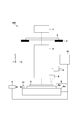
- FIG. 1 is a schematic diagram showing the configuration of the exposure apparatus 100.
- the exposure apparatus 100 includes, for example, an illumination optical system 1, a mask stage 3 that holds a mask 2, a projection optical system 4, a substrate stage 6 that holds a substrate 5, a position measurement unit 7, and a focus detection unit 8.
- the processing unit 9 and the control unit 10 can be included.
- the control unit 10 is configured by, for example, a computer having a CPU, a memory, and the like, and controls processing for transferring the pattern of the mask 2 to the substrate 5 (processing for exposing the substrate 5).
- the illumination optical system 1 uniformly illuminates the mask 2 held by the mask stage 3 using light emitted from a light source (not shown).
- the projection optical system 4 has a predetermined projection magnification and projects the pattern of the mask 2 onto the substrate 5.
- the substrate stage 6 includes, for example, a substrate chuck 6 a that holds the substrate 5 and a substrate driving unit 6 b that drives the substrate chuck 6 a (substrate 5), and a direction (XY direction) orthogonal to the optical axis of the projection optical system 4. It is configured to be movable.
- the position measurement unit 7 includes a laser interferometer, for example, and measures the position of the substrate stage 6.
- the laser interferometer irradiates the reflecting plate 11 provided on the substrate stage 6 with laser light, and detects the displacement of the substrate stage 6 using the laser light reflected by the reflecting plate 11. Thereby, the position measurement unit 7 can obtain the current position of the substrate stage 6 based on the displacement detected by the laser interferometer.
- the focus detection unit 8 detects the height of the detection target location in the detection area.
- the focus detection unit 8 may include a light source that obliquely makes light incident on the surface of the substrate 5 and an image sensor having a plurality of pixels that are two-dimensionally arranged. Then, the focus detection unit 8 is a detection target in the area where the light is obliquely incident (in the detection area) on the surface of the substrate 5 based on the position on the image sensor where the light reflected by the surface of the substrate is incident. Detect the height of the location.
- the processing unit 9 is configured by a computer including a CPU and a memory, for example, and obtains the height distribution of the surface of the substrate 5 based on the detection result of the focus detection unit 8. For example, the processing unit 9 causes the focus detection unit to scan the substrate 5 and the detection area of the focus detection unit 8 relatively in one of the in-plane directions (XY directions) of the substrate 5 with the substrate stage 6. 8 is caused to detect the height of the surface of the substrate 5 in the detection region. Accordingly, the processing unit 9 can obtain the height distribution of the surface of the substrate 5 in the one direction (scanning direction).
- the processing unit 9 of the present embodiment is configured separately from the control unit 10, but may be configured integrally with the control unit 10.
- the focus detection unit 8 and the processing unit 9 constitute a measurement device that measures the height distribution of the surface of the substrate 5.
- the measurement apparatus is provided inside the exposure apparatus 100, but may be provided outside the exposure apparatus 100.
- the surface of the substrate 5 is an image plane (focus plane) of the projection optical system 4 according to the position on the substrate to be exposed (position of the shot area).
- the projection image of the projection optical system 4 can be controlled by the control unit 10 so as to be disposed at the position.
- the projection image is controlled by driving an optical element (lens) provided in the projection optical system 4 or driving the substrate 5 by the substrate stage 6 in a direction parallel to the optical axis of the projection optical system 4. Can be done. Therefore, in the exposure apparatus 100, it is preferable to obtain distribution information indicating the height distribution in the plane of the substrate 5 (the entire surface of the substrate 5) in advance.
- the detection area is scanned over the entire surface of the substrate and the height of the surface is detected by the focus detection unit 8, the detection requires a corresponding time, which is disadvantageous in terms of throughput. Can be.
- the measurement apparatus uses the tendency (feature) of the height distribution in the plane of the substrate 5 caused by the manufacturing method of the substrate 5 to make the substrate 5 and the detection region relative to each other.
- the focus detection unit 8 detects the height of the surface of the substrate 5. That is, in the measurement apparatus of the first embodiment, distribution information is generated without detecting the height of the surface of the substrate 5 by the focus detection unit 8 over the entire surface of the substrate 5. Thereby, the time for measuring the height distribution of the surface of the substrate 5 can be greatly shortened.
- generation method of distribution information are demonstrated.
- the tendency of the height distribution of the surface of the substrate 5 resulting from the manufacturing method of the substrate 5 will be described.
- the glass substrate is manufactured (made by a plate) by stretching in one direction using a float method, a fusion method, or the like.
- the thickness can be made substantially uniform in the stretching direction, but in the direction orthogonal to the stretching direction (hereinafter referred to as the orthogonal direction) Variations in thickness can occur due to typical temperature fluctuations and temperature fluctuations.
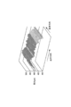
- the variation in thickness in the stretching direction of the glass substrate is 1 While the thickness is 0.4 ⁇ m, the thickness variation in the orthogonal direction is 12 ⁇ m. That is, the thickness variation in the orthogonal direction is about one digit larger than the thickness variation in the stretching direction. This indicates that the thickness distribution in the orthogonal direction (that is, the surface height distribution in the orthogonal direction) has the same tendency for each of a plurality of positions in the stretching direction.
- the height distribution of the surface of the substrate 5 in the orthogonal direction can be measured, the height of the entire surface of the substrate 5 is interpolated (estimated) from the measurement result, and the height distribution of the entire surface of the substrate 5 is calculated. Can be requested.
- the height variation in the other can be larger than the height variation in one of the first and second directions different from each other.
- the first direction and the second direction may be directions parallel to two sides orthogonal to each other among the sides of the surface of the glass substrate (substrate 5).
- the processing unit 9 obtains the height distribution of the surface of the substrate 5 in the first direction as the first distribution by relatively scanning the substrate 5 and the detection area of the focus detection unit 8 in the first direction. At this time, if the height variation in the first distribution is greater than or equal to the reference value, the first direction corresponds to the orthogonal direction where the height variation is large. On the other hand, when the height variation in the first distribution is smaller than the reference value, the second direction corresponds to the orthogonal direction. In this case, the processing unit 9 obtains the height distribution of the surface of the substrate 5 in the second direction by relatively scanning the substrate 5 and the detection area of the focus detection unit 8 in the second direction.
- the reference value is set to a value between the thickness variation that can occur in the stretching direction of the substrate 5 (glass substrate) and the thickness variation that can occur in the orthogonal direction.
- the “height (of the surface of the substrate)” in the present embodiment may include the concept of “thickness (of the substrate)”. That is, the “height distribution (of the substrate surface)” may include the concept of “thickness distribution (of the substrate)”.
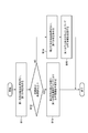
- FIG. 3 is a flowchart illustrating a method for generating distribution information
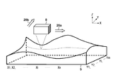
- FIG. 4 is a diagram illustrating a state in which the height of the surface of the substrate 5 is detected by the focus detection unit 8. Further, each step of the flowchart shown in FIG. 3 can be performed by the processing unit 9.
- the processing unit 9 causes the focus detection unit 8 to scan the substrate 5 and the detection area of the focus detection unit 8 relatively in the first direction (for example, the X direction) as indicated by an arrow 20a in FIG. Processing for detecting the height of the surface of the substrate 5 (detection processing in the first direction) is performed.
- the detection process in the first direction may be performed a plurality of times, but is preferably performed only once from the viewpoint of throughput. Thereby, the processing unit 9 can obtain the height distribution of the surface of the substrate 5 in the first direction.
- the height distribution of the surface of the substrate 5 in the first direction performed in step S11 is referred to as a “first distribution”.
- the detection process in the first direction in S11 can be performed at an arbitrary position (coordinates) in the second direction.
- the processing unit 9 determines whether or not the height variation in the first distribution is greater than or equal to a reference value.
- a reference value such as a standard deviation in the first distribution can be used. May be used. If the height variation in the first distribution is greater than or equal to the reference value, it is determined (specified) that the first direction corresponds to an orthogonal direction in which the height variation of the surface of the substrate 5 is relatively large, and the process proceeds to S13. move on. In this case, the processing unit 9 generates distribution information from the first distribution without relatively scanning the substrate 5 and the detection area of the focus detection unit 8 in the second direction.
- the processing unit 9 also generates distribution information by estimating that the height distribution of the surface of the substrate 5 in the direction parallel to the first direction is the first distribution for each of the plurality of positions in the second direction. To do. For example, the processing unit 9 distributes by applying the first distribution as it is as the height distribution of the surface of the substrate 5 in each of a plurality of directions parallel to the first direction and passing through a plurality of positions in the second direction. Generate information. As described above, since the variation in the thickness of the substrate 5 is very small in the extending direction of the substrate 5, it can be assumed that the variation in the thickness does not occur. Therefore, the processing unit 9 can reduce an error with respect to the actual height distribution of the surface of the substrate 5 even if the distribution information is generated using only the first distribution as described above.
- the processing unit 9 causes the focus detection unit 8 to scan the substrate 5 and the detection area of the focus detection unit 8 relatively in the second direction (for example, the Y direction) as indicated by an arrow 20b in FIG. Processing for detecting the height of the surface of the substrate 5 (detection processing in the second direction) is performed.
- the detection process in the second direction may be performed a plurality of times, but is preferably performed only once from the viewpoint of throughput. Accordingly, the processing unit 9 can obtain a height distribution in the second direction on the substrate 5.
- the height distribution in the second direction obtained in step S14 is hereinafter referred to as “second distribution”.
- the detection process in the second direction in S14 can be performed at an arbitrary position (coordinates) in the first direction.
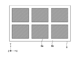
- a plurality of pattern areas 5a shots areas in which a base pattern (device pattern) has already been formed are arranged on the target substrate 5 on which the surface height is detected by the measuring device. There may be.
- the height detection by the focus detection unit 8 is preferably performed in a gap region 5b (scribe region) provided between the plurality of pattern regions 5a.
- the processing unit 9 defines the substrate 5 and the detection region so that the focus detection unit 8 detects the height in the gap region 5b based on the layout information indicating the layout (arrangement) of the plurality of pattern regions 5a. It is preferable to scan relatively.
- the layout information may be acquired, for example, by actually measuring the positions of the plurality of pattern areas 5a, or may be design information on the positions of the plurality of pattern areas 5a.
- the processing unit 9 determines the height of the undetected portion of the surface of the substrate 5 that has not been detected by the focus detection unit 8 based on the first distribution acquired in S11 and the second distribution acquired in S14. Distribution information is generated by interpolation (estimation). The interpolation of the height of the undetected portion is a result of correcting the first distribution with the height at the predetermined position in the second distribution as a height distribution in a direction passing through the predetermined position in the second direction and parallel to the first direction. This can be done by applying
- the processing unit 9 obtains the first distribution by performing the detection process in the first direction at the position Y1 in the second direction, and in the process of S14, the second distribution is performed at the position X1 in the first direction. It is assumed that the second distribution is acquired by performing the direction detection process. In this case, the processing unit 9 uses the height at the position Y1 and the height at the position Yi obtained from the second distribution as the height distribution in the direction parallel to the first direction and passing through the position Yi in the second direction. The result (distribution) obtained by correcting the first distribution with the difference is applied.
- the processing unit 9 generates distribution information by interpolating the height of the undetected portion by applying the result of correcting the first distribution in the same manner for each of the plurality of positions in the second direction.
- the distribution information is generated using both the first distribution and the second distribution, but the present invention is not limited to this, and the distribution information may be generated using only the second distribution.
- the measurement device when the height variation in the first distribution obtained by the detection process in the first direction is greater than or equal to the reference value, the measurement device according to the first embodiment generates distribution information based on the first distribution. Generate.
- the second distribution is obtained by performing detection processing in the second direction, and distribution information is generated based on the first distribution and the second distribution.
- the measurement apparatus may perform only the process of obtaining the first distribution or the first distribution and the second distribution, and the process of generating the distribution information may be performed by the control unit 10 of the exposure apparatus 100, an external computer, or the like.
- the processing unit 9 acquires distribution information generated by the control unit 10 of the exposure apparatus 100, an external computer, or the like.
- FIG. 6 is a flowchart illustrating a distribution information generation method according to the second embodiment. Each step of the flowchart shown in FIG. 6 can be performed by the processing unit 9.
- the processing unit 9 performs detection processing in the first direction.
- the detection process in the first direction may be performed a plurality of times, but is preferably performed only once from the viewpoint of throughput. Thereby, the processing unit 9 can obtain the height distribution of the surface of the substrate 5 in the first direction.
- the height distribution of the surface of the substrate 5 in the first direction obtained in the step S21 is hereinafter referred to as “first distribution”.
- the detection process in the first direction can be performed at an arbitrary position (coordinates) in the second direction.
- the processing unit 9 performs detection processing in the second direction.
- the detection process in the second direction may be performed a plurality of times, but is preferably performed only once from the viewpoint of throughput. Thereby, the processing unit 9 can obtain the height distribution of the surface of the substrate 5 in the second direction.
- the height distribution of the surface of the substrate 5 in the second direction obtained in the step S22 is hereinafter referred to as “second distribution”.
- the detection process in the second direction can be performed at an arbitrary position (coordinates) in the first direction.
- the processing unit 9 In S23, the processing unit 9 generates distribution information by interpolating (estimating) the height of the undetected portion based on the first distribution acquired in S21 and the second distribution acquired in S22. Since the process of S23 is the same as the process of S15 in the flowchart of FIG. 3, a description thereof is omitted here. By generating the distribution information in this way, the time required for measuring the height distribution of the surface of the substrate 5 can be greatly shortened, which can be advantageous in terms of throughput.
- the processing unit 9 causes the focus detection unit 8 to detect the height of the holding surface of the substrate stage 6 (substrate chuck 6a) in advance, and acquires information indicating the height distribution of the holding surface. Then, the processing unit 9 obtains information indicating the thickness distribution of the substrate 5 based on the result of the focus detection unit 8 detecting the thickness of the substrate 5 according to the flowchart shown in FIG. 3 or FIG.
- the processing unit 9 performs the in-plane height of the substrate 5 held by the substrate stage 6 based on the information indicating the height distribution of the holding surface of the substrate stage 6 and the information indicating the thickness distribution of the substrate 5.
- Information indicating the distribution can be obtained.
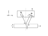
- the focus detection unit 8 includes, for example, a light source 8a that emits light having a wavelength of about 500 to 1200 nm and an image sensor 8b that is configured by a CCD, a CMOS, or the like, and the light emitted from the light source 8a is emitted from the substrate 5 (for example, The glass substrate) may be configured to be obliquely incident.
- the light emitted from the light source 8a (position A) and obliquely incident on the position B on the surface of the substrate 5 is divided into light reflected by the surface of the substrate 5 and light traveling inside the substrate.
- the light reflected by the surface of the substrate 5 enters the position E on the image sensor.
- the light traveling inside the substrate 5 is reflected at the position C on the back surface of the substrate 5, passes through the position D on the surface of the substrate 5, and enters the position F on the image sensor. Since the difference between the position E and the position F on the image sensor corresponds to the thickness t of the substrate 5, the focus detection unit 8 can obtain the thickness t of the substrate 5 based on the difference.
- the method for manufacturing an article in the embodiment of the present invention is suitable for manufacturing an article such as an electronic device such as a semiconductor device or an element having a fine structure.
- a latent image pattern is formed on the photosensitive agent applied to the substrate using the above-described exposure apparatus (a step of exposing the substrate), and the latent image pattern is formed in this step.
- the manufacturing method includes other well-known steps (oxidation, film formation, vapor deposition, doping, planarization, etching, resist stripping, dicing, bonding, packaging, and the like).
- the method for manufacturing an article according to the present embodiment is advantageous in at least one of the performance, quality, productivity, and production cost of the article as compared with the conventional method.
- the present invention supplies a program that realizes one or more functions of the above-described embodiments to a system or apparatus via a network or a storage medium, and one or more processors in a computer of the system or apparatus read and execute the program This process can be realized. It can also be realized by a circuit (for example, ASIC) that realizes one or more functions.
- a circuit for example, ASIC
Landscapes
- Physics & Mathematics (AREA)
- General Physics & Mathematics (AREA)
- Length Measuring Devices By Optical Means (AREA)
- Exposure And Positioning Against Photoresist Photosensitive Materials (AREA)
- Exposure Of Semiconductors, Excluding Electron Or Ion Beam Exposure (AREA)
Abstract
互いに異なる第1方向および第2方向のうちの一方における高さばらつきより他方における高さばらつきの方が大きい面を有する基板に対し、当該面の高さ分布を計測する計測装置は、検出領域内の検出対象箇所の高さを検出する検出部と、前記基板と前記検出領域とを相対的に走査させることにより走査方向における前記基板の面の高さ分布を求める処理部と、を含み、前記処理部は、前記第1方向に前記基板と前記検出領域とを相対的に走査させることにより前記第1方向における前記基板の面の高さ分布を第1分布として求め、前記第1分布における高さばらつきが基準値以上か否かを判断し、前記第1分布における高さばらつきが基準値より小さいと判断した場合には、前記第2方向に前記基板と前記検出領域とを相対的に走査させることにより前記第2方向における前記基板の面の高さ分布を求める。
Description
本発明は、基板の面の高さ分布を計測する計測装置、露光装置、および物品の製造方法に関する。
液晶パネルや有機ELパネル等のフラットパネル、もしくは半導体デバイスの製造には、レジストが塗布されたガラスプレートやウェハなどの基板に、マスクのパターンを投影光学系を介して転写する露光装置が用いられる。このような露光装置では、基板の露光中、露光すべき基板上の位置に応じて基板の表面を投影光学系の結像面(フォーカス面)に配置するため、基板の面の高さ分布を事前に求めておくことが好ましい。特許文献1には、基板の厚さ分布と、当該基板が保持される保持面の高さ分布とをそれぞれ事前に計測することにより、その計測結果に基づいて、保持面に保持された基板の面の高さ分布を求める方法が提案されている。
基板の面の高さ分布を計測する計測装置には、検出領域内の検出対象箇所の高さを検出するものがある。このような計測装置では、基板と検出領域とを相対的に走査しながら検出領域における基板の面の高さを検出することにより基板の面の高さ分布を計測することができる。しかしながら、基板の面の全体にわたって検出領域を走査して当該面の高さの検出を行うと、当該検出に相応の時間を要してしまい、スループットの点で不利になりうる。
そこで、本発明は、基板の面の高さ分布を計測する時間を短縮するために有利な技術を提供することを目的とする。
上記目的を達成するために、本発明の一側面としての計測装置は、互いに異なる第1方向および第2方向のうちの一方における高さばらつきより他方における高さばらつきの方が大きい面を有する基板に対し、当該面の高さ分布を計測する計測装置であって、検出領域内の検出対象箇所の高さを検出する検出部と、前記基板と前記検出領域とを相対的に走査させることにより走査方向における前記基板の面の高さ分布を求める処理部と、を含み、前記処理部は、前記第1方向に前記基板と前記検出領域とを相対的に走査させることにより前記第1方向における前記基板の面の高さ分布を第1分布として求め、前記第1分布における高さばらつきが基準値以上か否かを判断し、前記第1分布における高さばらつきが基準値より小さいと判断した場合には、前記第2方向に前記基板と前記検出領域とを相対的に走査させることにより前記第2方向における前記基板の面の高さ分布を求める、ことを特徴とする。
本発明によれば、例えば、基板の面の高さ分布を計測する時間を短縮するために有利な技術を提供することができる。
本発明のその他の特徴及び利点は、添付図面を参照とした以下の説明により明らかになるであろう。なお、添付図面においては、同じ若しくは同様の構成には、同じ参照番号を付す。
添付図面は明細書に含まれ、その一部を構成し、本発明の実施の形態を示し、その記述と共に本発明の原理を説明するために用いられる。
露光装置の構成を示す概略図である。
ガラス基板の厚さのばらつきを示す図である。
第1実施形態に係る分布情報の生成方法を示すフローチャートである。
フォーカス検出部によって基板の面の高さを検出している様子を示す図である。
複数のパターン領域を有する基板を示す図である。
第2実施形態に係る分布情報の生成方法を示すフローチャートである。
基板の厚さの検出原理を説明するための図である。
以下、添付図面を参照して、本発明の好適な実施の形態について説明する。なお、各図において、同一の部材ないし要素については同一の参照番号を付し、重複する説明は省略する。
<第1実施形態>
本発明に係る第1実施形態の露光装置100について、図1を参照しながら説明する。図1は、露光装置100の構成を示す概略図である。露光装置100は、例えば、照明光学系1と、マスク2を保持するマスクステージ3と、投影光学系4と、基板5を保持する基板ステージ6と、位置計測部7と、フォーカス検出部8と、処理部9と、制御部10とを含みうる。制御部10は、例えば、CPUやメモリなどを有するコンピュータによって構成され、マスク2のパターンを基板5に転写する処理(基板5を露光する処理)を制御する。
本発明に係る第1実施形態の露光装置100について、図1を参照しながら説明する。図1は、露光装置100の構成を示す概略図である。露光装置100は、例えば、照明光学系1と、マスク2を保持するマスクステージ3と、投影光学系4と、基板5を保持する基板ステージ6と、位置計測部7と、フォーカス検出部8と、処理部9と、制御部10とを含みうる。制御部10は、例えば、CPUやメモリなどを有するコンピュータによって構成され、マスク2のパターンを基板5に転写する処理(基板5を露光する処理)を制御する。
照明光学系1は、光源(不図示)から射出された光を用いて、マスクステージ3により保持されたマスク2を均一に照明する。投影光学系4は、所定の投影倍率を有し、マスク2のパターンを基板5に投影する。基板ステージ6は、例えば、基板5を保持する基板チャック6aと、基板チャック6a(基板5)を駆動する基板駆動部6bとを含み、投影光学系4の光軸と直交する方向(XY方向)に移動可能に構成される。位置計測部7は、例えばレーザ干渉計を含み、基板ステージ6の位置を計測する。レーザ干渉計は、基板ステージ6に設けられた反射板11にレーザ光を照射し、反射板11で反射されたレーザ光を用いて基板ステージ6の変位を検出する。これにより、位置計測部7は、レーザ干渉計で検出された変位に基づいて基板ステージ6の現在位置を求めることができる。
フォーカス検出部8は、検出領域内の検出対象箇所の高さを検出する。例えば、フォーカス検出部8は、基板5の面に光を斜入射させる光源と、二次元的に配列した複数の画素を有するイメージセンサとを含みうる。そして、フォーカス検出部8は、基板の面で反射された光が入射するイメージセンサ上の位置に基づいて、基板5の面のうち、光が斜入射した領域内(検出領域内)の検出対象箇所の高さを検出する。
処理部9は、例えばCPUやメモリなどを含むコンピュータによって構成され、フォーカス検出部8での検出結果に基づいて基板5の面の高さ分布を求める。例えば、処理部9は、基板5の面内方向(XY方向)のうちの一方向に、基板ステージ6によって基板5とフォーカス検出部8の検出領域とを相対的に走査させながら、フォーカス検出部8に検出領域内での基板5の面の高さを検出させる。これにより、処理部9は、当該一方向(走査方向)における基板5の面の高さ分布を得ることができる。ここで、本実施形態の処理部9は、制御部10と別々に構成されているが、制御部10と一体に構成されてもよい。また、フォーカス検出部8および処理部9は、基板5の面の高さ分布を計測する計測装置を構成する。本実施形態では、該計測装置が露光装置100の内部に設けられているが、露光装置100の外部に設けられてもよい。
このように構成された露光装置100では、基板5の露光中、露光すべき基板上の位置(ショット領域の位置)に応じて基板5の面が投影光学系4の結像面(フォーカス面)に配置されるように、投影光学系4の投影像が制御部10によって制御されうる。当該投影像の制御は、例えば、投影光学系4に設けられた光学素子(レンズ)を駆動したり、投影光学系4の光軸と平行な方向に基板5を基板ステージ6によって駆動したりすることによって行われうる。そのため、露光装置100では、基板5の面内(基板5の面の全体)における高さ分布を示す分布情報を事前に取得しておくことが好ましい。しかしながら、計測装置において、基板の面の全体にわたって検出領域を走査して当該面の高さをフォーカス検出部8に検出させると、当該検出に相応の時間を要してしまい、スループットの点で不利になりうる。
そこで、第1実施形態の計測装置は、基板5の製造方法に起因して生じる基板5の面内における高さ分布の傾向(特徴)を利用することにより、基板5と検出領域とを相対的に走査してフォーカス検出部8に基板5の面の高さを検出させる回数を低減させる。つまり、第1実施形態の計測装置では、フォーカス検出部8による基板5の面の高さの検出を基板5の面の全体にわたって行うことなく分布情報を生成する。これにより、基板5の面の高さ分布を計測する時間を大幅に短縮することができる。以下に、基板5の製造方法に起因して生じる基板5の面の高さ分布の傾向、および分布情報の生成方法について説明する。
まず、基板5の製造方法に起因して生じる基板5の面の高さ分布の傾向について説明する。例えば、液晶デバイス等で使用される透明な矩形形状のガラス基板を基板5として用いる場合を想定する。ガラス基板は、フロート法やフュージョン法などを用いて、ある一方向に延伸させることにより製造(製板)される。このような製造方法により作製されたガラス基板では、延伸方向においては厚さをほぼ均一にすることができるが、延伸方向と直交する方向(以下、直交方向)においては、製造中における周囲の局所的な温度変動や温度揺らぎによって厚さにばらつきが生じうる。
例えば、厚さが500μm、大きさが1.5×1.8mの矩形形状を有するガラス基板を実際に製造すると、図2に示すように、ガラス基板の延伸方向での厚さのばらつきは1.4μmであるのに対し、直交方向での厚さのばらつきは12μmとなる。即ち、直交方向での厚さばらつきは、延伸方向での厚さばらつきと比べて約1桁大きい。これは、直交方向での厚さ分布(即ち、直交方向での表面高さ分布)が、延伸方向の複数位置の各々について同様の傾向となることを示している。したがって、直交方向における基板5の面の高さ分布を測定することができれば、その計測結果から基板5の面の全体における高さを補間(推定)し、基板5の面の全体における高さ分布を求めることができる。
このように、ガラス基板の面(露光処理を行うべき面)では、互いに異なる第1方向および第2方向のうちの一方における高さばらつきより他方における高さばらつきの方が大きくなりうる。ここで、第1方向および第2方向は、ガラス基板(基板5)の面の辺のうち互いに直交する2つの辺にそれぞれ平行な方向でありうる。しかしながら、当該ガラス基板の面の高さ分布を計測する際では、第1方向および第2方向のうちのどちらが、高さばらつき(厚さばらつき)の大きい直交方向であるのかが不明である。
そこで、処理部9は、第1方向に基板5とフォーカス検出部8の検出領域とを相対的に走査させることにより第1方向における基板5の面の高さ分布を第1分布として求める。このとき、第1分布における高さばらつきが基準値以上であれば、第1方向が、高さばらつきの大きい直交方向に対応していることとなる。一方、第1分布における高さばらつきが基準値より小さい場合では、第2方向が直交方向に対応していることとなる。この場合、処理部9は、第2方向に基板5とフォーカス検出部8の検出領域とを相対的に走査させることにより第2方向における基板5の面の高さ分布を求める。ここで、基準値は、基板5(ガラス基板)の延伸方向に生じうる厚さのばらつきと、直交方向に生じうる厚さのばらつきとの間の値に設定される。また、本実施形態における「(基板の面の)高さ」は、「(基板の)厚さ」の概念を含みうる。即ち、「(基板の面の)高さ分布」は、「(基板の)厚さ分布」の概念を含みうる。
次に、分布情報の生成方法について、図3および図4を参照しながら説明する。図3は、分布情報の生成方法を示すフローチャートであり、図4は、フォーカス検出部8によって基板5の面の高さを検出している様子を示す図である。また、図3に示すフローチャートの各工程は、処理部9によって行われうる。
S11では、処理部9は、図4の矢印20aで示すように、第1方向(例えばX方向)に基板5とフォーカス検出部8の検出領域とを相対的に走査させながらフォーカス検出部8に基板5の面の高さを検出させる処理(第1方向の検出処理)を行う。第1方向の検出処理は、複数回行われてもよいが、スループットの観点から、1回だけ行われることが好ましい。これにより、処理部9は、第1方向における基板5の面の高さ分布を得ることができる。S11の工程でられた第1方向における基板5の面の高さ分布を、以下では「第1分布」と称する。ここで、S11における第1方向の検出処理は、第2方向における任意の位置(座標)で行われうる。
S12では、処理部9は、第1分布における高さばらつきが基準値以上か否かを判断する。第1分布における高さばらつきとしては、第1分布における高さの最大値と最小値との差が用いられうるが、それに限られるものではなく、例えば、第1分布における標準偏差などの値が用いられてもよい。第1分布における高さばらつきが基準値以上である場合には、第1方向が、基板5の面の高さばらつきが比較的大きい直交方向に対応していると判断(特定)してS13に進む。この場合、処理部9は、第2方向に基板5とフォーカス検出部8の検出領域とを相対的に走査させずに、第1分布から分布情報を生成する。
S13では、処理部9は、第2方向における複数の位置の各々についても、第1方向と平行な方向における基板5の面の高さ分布が第1分布であると推定して分布情報を生成する。例えば、処理部9は、第2方向における複数の位置をそれぞれ通り且つ第1方向に平行な複数の方向の各々における基板5の面の高さ分布として、第1分布をそのまま適用することにより分布情報を生成する。上述したように、基板5の延伸方向では、基板5の厚さのばらつきが非常に小さいため、当該厚さのばらつきが生じていないものと仮定することができる。そのため、処理部9は、上述のように第1分布のみを用いて分布情報を生成しても、実際の基板5の面の高さ分布に対する誤差を小さくすることができる。
一方、S12において、第1分布における高さばらつきが基準値より小さい場合には、第2方向が基板5の直交方向に対応していると判断(特定)してS14に進む。S14では、処理部9は、図4の矢印20bで示すように、第2方向(例えばY方向)に基板5とフォーカス検出部8の検出領域とを相対的に走査させながらフォーカス検出部8に基板5の面の高さを検出させる処理(第2方向の検出処理)を行う。第2方向の検出処理は、複数回行われてもよいが、スループットの観点から、1回だけ行われることが好ましい。これにより、処理部9は、基板5における第2方向の高さ分布を得ることができる。S14の工程で得られた第2方向の高さ分布を、以下では「第2分布」と称する。ここで、S14における第2方向の検出処理は、第1方向における任意の位置(座標)で行われうる。
計測装置により面の高さの検出が行われる対象の基板5には、図5に示すように、下地パターン(デバイスパターン)が既に形成された複数のパターン領域5a(ショット領域)が配列している場合がある。この場合、S11およびS14において、フォーカス検出部8によってパターン領域内の高さを検出してしまうと、当該パターン領域5aに形成された下地パターンによって、検出結果に誤差が生じることがある。そのため、フォーカス検出部8による高さの検出は、複数のパターン領域5aの間に設けられた間隙領域5b(スクライブ領域)において行われることが好ましい。したがって、処理部9は、複数のパターン領域5aのレイアウト(配置)を示すレイアウト情報に基づいて、間隙領域5bにおいてフォーカス検出部8による高さの検出が行われるように基板5と検出領域とを相対的に走査させることが好ましい。レイアウト情報は、例えば、複数のパターン領域5aの位置を実際に計測することによって取得されてもよいし、複数のパターン領域5aの位置の設計情報であってもよい。
S15では、処理部9は、S11で取得した第1分布とS14で取得した第2分布とに基づいて、基板5の面のうちフォーカス検出部8による検出が行われていない未検出部分の高さを補間(推定)することにより分布情報を生成する。未検出部分の高さの補間は、第2方向の所定位置を通り且つ第1方向と平行な方向における高さ分布として、第2分布における所定位置での高さで第1分布を補正した結果を適用することにより行われうる。
例えば、処理部9は、S11の工程では、第2方向の位置Y1において第1方向の検出処理を行うことにより第1分布を取得し、S14の工程では、第1方向の位置X1において第2方向の検出処理を行うことにより第2分布を取得したとする。この場合、処理部9は、第2方向の位置Yiを通り且つ第1方向と平行な方向における高さ分布として、第2分布から得られた位置Y1での高さと位置Yiでの高さとの差で第1分布を補正した結果(分布)を適用する。このように、処理部9は、第2方向における複数の位置の各々についても同様に第1分布を補正した結果を適用することで、未検出部分の高さを補間して分布情報を生成することができる。ここで、S15では、第1分布および第2分布の双方を用いて分布情報を生成したが、それに限られるものではなく、第2分布のみを用いて分布情報を生成してもよい。
上述したように、第1実施形態の計測装置は、第1方向の検出処理により得られた第1分布における高さばらつきが基準値以上である場合には、第1分布に基づいて分布情報を生成する。一方、第1分布における高さばらつきが基準値より小さい場合には、第2方向の検出処理を行うことにより第2分布を求め、第1分布および第2分布に基づいて分布情報を生成する。このように基板5の面の高さ分布を計測することにより、高さ分布の計測に要する時間を大幅に短縮することができ、スループットの点で有利となりうる。ここで、第1実施形態では、計測装置(処理部9)が分布情報を生成する処理を行う例について説明したが、それに限られるものではない。例えば、計測装置が、第1分布、若しくは第1分布および第2分布を求める処理のみを行い、分布情報を生成する処理は、露光装置100の制御部10や外部コンピュータなどによって行われてもよい。この場合、処理部9は、露光装置100の制御部10や外部コンピュータなどで生成された分布情報を取得することとなる。
<第2実施形態>
第2実施形態では、分布情報の生成方法についての他の例を説明する。第2実施形態では、第1方向の検出処理および第2方向の検出処理を初めに行い、それにより得られた第1分布と第2分布とに基づいて未検出部分の高さを補間(推定)することにより分布情報を生成する。図6は、第2実施形態に係る分布情報の生成方法を示すフローチャートである。図6に示すフローチャートの各工程は、処理部9によって行われうる。
第2実施形態では、分布情報の生成方法についての他の例を説明する。第2実施形態では、第1方向の検出処理および第2方向の検出処理を初めに行い、それにより得られた第1分布と第2分布とに基づいて未検出部分の高さを補間(推定)することにより分布情報を生成する。図6は、第2実施形態に係る分布情報の生成方法を示すフローチャートである。図6に示すフローチャートの各工程は、処理部9によって行われうる。
S21では、処理部9は、第1方向の検出処理を行う。第1方向の検出処理は、複数回行われてもよいが、スループットの観点から、1回だけ行われることが好ましい。これにより、処理部9は、第1方向における基板5の面の高さ分布を得ることができる。S21の工程で得られた第1方向における基板5の面の高さ分布を、以下では「第1分布」と称する。ここで、第1方向の検出処理は、第2方向における任意の位置(座標)で行われうる。
S22では、処理部9は、第2方向の検出処理を行う。第2方向の検出処理は、複数回行われてもよいが、スループットの観点から、1回だけ行われることが好ましい。これにより、処理部9は、第2方向における基板5の面の高さ分布を得ることができる。S22の工程で得られた第2方向における基板5の面の高さ分布を、以下では「第2分布」と称する。ここで、第2方向の検出処理は、第1方向における任意の位置(座標)で行われうる。
S23では、処理部9は、S21で取得した第1分布とS22で取得した第2分布とに基づいて、未検出部分の高さを補間(推定)することにより分布情報を生成する。S23の工程は、図3のフローチャートにおけるS15の工程と同様であるため、ここでの説明を省略する。このように分布情報を生成することにより、基板5の面の高さ分布の計測に要する時間を大幅に短縮することができ、スループットの点で有利となりうる。
<第3実施形態>
第1実施形態および第2実施形態では、フォーカス検出部8によって基板5の面の高さを検出する例について説明したが、第3実施形態では、基板5の面の高さの代わりに基板5の厚さを検出する例について説明する。この場合、処理部9は、基板ステージ6(基板チャック6a)の保持面の高さをフォーカス検出部8に事前に検出させ、当該保持面の高さ分布を示す情報を取得しておく。そして、処理部9は、図3または図6に示すフローチャートに従って基板5の厚さをフォーカス検出部8に検出させた結果に基づいて、基板5の厚さ分布を示す情報を求める。これにより、処理部9は、基板ステージ6の保持面の高さ分布を示す情報と基板5の厚さ分布を示す情報とに基づいて、基板ステージ6よって保持された基板5の面内の高さ分布を示す情報(分布情報)を求めることができる。
第1実施形態および第2実施形態では、フォーカス検出部8によって基板5の面の高さを検出する例について説明したが、第3実施形態では、基板5の面の高さの代わりに基板5の厚さを検出する例について説明する。この場合、処理部9は、基板ステージ6(基板チャック6a)の保持面の高さをフォーカス検出部8に事前に検出させ、当該保持面の高さ分布を示す情報を取得しておく。そして、処理部9は、図3または図6に示すフローチャートに従って基板5の厚さをフォーカス検出部8に検出させた結果に基づいて、基板5の厚さ分布を示す情報を求める。これにより、処理部9は、基板ステージ6の保持面の高さ分布を示す情報と基板5の厚さ分布を示す情報とに基づいて、基板ステージ6よって保持された基板5の面内の高さ分布を示す情報(分布情報)を求めることができる。
ここで、フォーカス検出部8によって基板5の厚さが検出される原理について、図7を参照しながら説明する。フォーカス検出部8は、例えば、波長が500~1200nm程度の光を射出する光源8aと、CCDやCMOS等で構成されたイメージセンサ8bとを含み、光源8aから射出された光を基板5(例えばガラス基板)に斜入射させるように構成されうる。光源8a(位置A)から射出されて基板5の表面の位置Bに斜入射した光は、基板5の表面で反射される光と基板の内部に進む光とに分けられる。基板5の表面で反射された光は、イメージセンサ上の位置Eに入射する。一方、基板5の内部に進んだ光は、基板5の裏面の位置Cで反射されて基板5の表面の位置Dを透過し、イメージセンサ上の位置Fに入射する。このイメージセンサ上の位置Eと位置Fとの差が基板5の厚さtに対応するため、フォーカス検出部8は、当該差に基づいて基板5の厚さtを求めることができる。
<物品の製造方法の実施形態>
本発明の実施形態における物品の製造方法は、例えば、半導体デバイス等の電子デバイスや微細構造を有する素子等の物品を製造するのに好適である。本実施形態の物品の製造方法は、基板に塗布された感光剤に上記の露光装置を用いて潜像パターンを形成する工程(基板を露光する工程)と、かかる工程で潜像パターンが形成された基板を現像する工程とを含む。更に、かかる製造方法は、他の周知の工程(酸化、成膜、蒸着、ドーピング、平坦化、エッチング、レジスト剥離、ダイシング、ボンディング、パッケージング等)を含む。本実施形態の物品の製造方法は、従来の方法に比べて、物品の性能・品質・生産性・生産コストの少なくとも1つにおいて有利である。
本発明の実施形態における物品の製造方法は、例えば、半導体デバイス等の電子デバイスや微細構造を有する素子等の物品を製造するのに好適である。本実施形態の物品の製造方法は、基板に塗布された感光剤に上記の露光装置を用いて潜像パターンを形成する工程(基板を露光する工程)と、かかる工程で潜像パターンが形成された基板を現像する工程とを含む。更に、かかる製造方法は、他の周知の工程(酸化、成膜、蒸着、ドーピング、平坦化、エッチング、レジスト剥離、ダイシング、ボンディング、パッケージング等)を含む。本実施形態の物品の製造方法は、従来の方法に比べて、物品の性能・品質・生産性・生産コストの少なくとも1つにおいて有利である。
<その他の実施例>
本発明は、上述の実施形態の1以上の機能を実現するプログラムを、ネットワーク又は記憶媒体を介してシステム又は装置に供給し、そのシステム又は装置のコンピュータにおける1つ以上のプロセッサーがプログラムを読出し実行する処理でも実現可能である。また、1以上の機能を実現する回路(例えば、ASIC)によっても実現可能である。
本発明は、上述の実施形態の1以上の機能を実現するプログラムを、ネットワーク又は記憶媒体を介してシステム又は装置に供給し、そのシステム又は装置のコンピュータにおける1つ以上のプロセッサーがプログラムを読出し実行する処理でも実現可能である。また、1以上の機能を実現する回路(例えば、ASIC)によっても実現可能である。
本発明は上記実施の形態に制限されるものではなく、本発明の精神及び範囲から離脱することなく、様々な変更及び変形が可能である。従って、本発明の範囲を公にするために、以下の請求項を添付する。
本願は、2016年8月5日提出の日本国特許出願特願2016-154946を基礎として優先権を主張するものであり、その記載内容の全てを、ここに援用する。
Claims (15)
- 互いに異なる第1方向および第2方向のうちの一方における高さばらつきより他方における高さばらつきの方が大きい面を有する基板に対し、当該面の高さ分布を計測する計測装置であって、
検出領域内の検出対象箇所の高さを検出する検出部と、
前記基板と前記検出領域とを相対的に走査させることにより走査方向における前記基板の面の高さ分布を求める処理部と、
を含み、
前記処理部は、前記第1方向に前記基板と前記検出領域とを相対的に走査させることにより前記第1方向における前記基板の面の高さ分布を第1分布として求め、前記第1分布における高さばらつきが基準値以上か否かを判断し、前記第1分布における高さばらつきが基準値より小さいと判断した場合には、前記第2方向に前記基板と前記検出領域とを相対的に走査させることにより前記第2方向における前記基板の面の高さ分布を求める、ことを特徴とする計測装置。 - 前記基板は、パターンが形成された複数のパターン領域と、前記複数のパターン領域の間に設けられた間隙領域とを含み、
前記処理部は、前記複数のパターン領域のレイアウト情報に基づいて、前記間隙領域において前記検出部による高さの検出が行われるように前記基板と前記検出領域とを相対的に走査させる、ことを特徴とする請求項1に記載の計測装置。 - 前記処理部は、前記第1方向に前記基板と前記検出領域とを相対的に1回だけ走査させることにより前記第1分布を求め、前記第1分布における高さばらつきが前記基準値より小さいと判断した場合には、前記第2方向に前記基板と前記検出領域とを相対的に1回だけ走査させることにより前記第2方向における前記基板の面の高さ分布を求める、ことを特徴とする請求項1又は2に記載の計測装置。
- 前記基板は、矩形形状を有し、
前記第1方向および前記第2方向は、前記基板の面の辺のうち互いに直交する2つの辺にそれぞれ平行である、ことを特徴とする請求項1乃至3のうちいずれか1項に記載の計測装置。 - 前記処理部は、前記第1分布における高さばらつきが前記基準値以上であると判断した場合には、前記第1分布から生成される前記基板の面内における高さ分布を示す分布情報を取得する、ことを特徴とする請求項1乃至4のうちいずれか1項に記載の計測装置。
- 前記処理部は、前記第1分布における高さばらつきが前記基準値以上であると判断した場合には、前記第1分布から前記基板の面内における高さ分布を示す分布情報を生成する、ことを特徴とする請求項1乃至4のうちいずれか1項に記載の計測装置。
- 前記処理部は、前記第1分布における高さばらつきが前記基準値以上であると判断した場合には、前記第2方向に前記基板と前記検出領域とを相対的に走査させずに、前記第1分布から前記基板の面内における高さ分布を示す分布情報を生成する、ことを特徴とする請求項1乃至4のうちいずれか1項に記載の計測装置。
- 前記処理部は、前記第1分布における高さばらつきが前記基準値以上であると判断した場合、前記第2方向における複数の位置をそれぞれ通り且つ前記第1方向に平行な複数の方向の各々における前記基板の面の高さ分布として前記第1分布をそのまま適用することにより前記分布情報を生成する、ことを特徴とする請求項5乃至7のうちいずれか1項に記載の計測装置。
- 前記処理部は、前記第1分布における高さばらつきが前記基準値より小さいと判断した場合には、前記第2方向における前記基板の面の高さ分布に基づいて、前記基板の面内における高さ分布を示す分布情報を生成する、ことを特徴とする請求項1乃至8のうちいずれか1項に記載の計測装置。
- 前記処理部は、前記第1分布における高さばらつきが前記基準値より小さいと判断した場合には、前記第1分布にも基づいて前記分布情報を生成する、ことを特徴とする請求項9に記載の計測装置。
- 前記処理部は、前記第1分布における高さばらつきが前記基準値より小さいと判断した場合、前記第1分布と前記第2方向における前記基板の面の高さ分布とに基づいて、前記基板の面のうち前記検出部による検出が行われていない未検出部分の高さを補間することにより、前記基板の面内における高さ分布を示す分布情報を生成する、ことを特徴とする請求項1乃至8のうちいずれか1項に記載の計測装置。
- 前記第1分布における高さばらつきは、前記第1分布における高さの最大値と最小値との差を含む、ことを特徴とする請求項1乃至11のうちいずれか1項に記載の計測装置。
- 前記基板を保持する保持面を有するステージを含み、
前記検出部は、前記基板の厚さを検出し、前記基板の厚さの検出結果および前記保持面の高さ分布を示す情報に基づいて、前記保持面により保持された前記基板の面の高さを求める、ことを特徴とする請求項1乃至12のうちいずれか1項に記載の計測装置。 - 基板を露光する露光装置であって、
マスクのパターンを前記基板に投影する投影光学系と、
前記基板の面の高さ分布を計測する請求項1乃至13のうちいずれか1項に記載の計測装置と、
前記計測装置での計測結果に基づいて、前記基板の露光を制御する制御部と、
を含むことを特徴とする露光装置。 - 請求項14に記載の露光装置を用いて基板を露光する工程と、
前記工程で露光された前記基板を現像する工程と、
を含み、現像された基板から物品を得ることを特徴とする物品の製造方法。
Priority Applications (2)
| Application Number | Priority Date | Filing Date | Title |
|---|---|---|---|
| CN201780048850.0A CN109564397B (zh) | 2016-08-05 | 2017-06-15 | 测量装置、曝光装置以及物品的制造方法 |
| KR1020197005133A KR102137986B1 (ko) | 2016-08-05 | 2017-06-15 | 계측 장치, 노광 장치 및 물품의 제조 방법 |
Applications Claiming Priority (2)
| Application Number | Priority Date | Filing Date | Title |
|---|---|---|---|
| JP2016-154946 | 2016-08-05 | ||
| JP2016154946A JP6704813B2 (ja) | 2016-08-05 | 2016-08-05 | 計測装置、露光装置、および物品の製造方法 |
Publications (1)
| Publication Number | Publication Date |
|---|---|
| WO2018025515A1 true WO2018025515A1 (ja) | 2018-02-08 |
Family
ID=61073384
Family Applications (1)
| Application Number | Title | Priority Date | Filing Date |
|---|---|---|---|
| PCT/JP2017/022039 Ceased WO2018025515A1 (ja) | 2016-08-05 | 2017-06-15 | 計測装置、露光装置、および物品の製造方法 |
Country Status (4)
| Country | Link |
|---|---|
| JP (1) | JP6704813B2 (ja) |
| KR (1) | KR102137986B1 (ja) |
| CN (1) | CN109564397B (ja) |
| WO (1) | WO2018025515A1 (ja) |
Cited By (1)
| Publication number | Priority date | Publication date | Assignee | Title |
|---|---|---|---|---|
| JP2022539239A (ja) * | 2019-07-04 | 2022-09-07 | エーエスエムエル ネザーランズ ビー.ブイ. | メトロロジにおける補正不能誤差 |
Families Citing this family (3)
| Publication number | Priority date | Publication date | Assignee | Title |
|---|---|---|---|---|
| US11610296B2 (en) * | 2020-01-09 | 2023-03-21 | Kla Corporation | Projection and distance segmentation algorithm for wafer defect detection |
| JP7475185B2 (ja) * | 2020-04-10 | 2024-04-26 | キヤノン株式会社 | 計測方法、インプリント装置及び物品の製造方法 |
| JP7489829B2 (ja) * | 2020-05-21 | 2024-05-24 | キヤノン株式会社 | 処理装置、計測方法および物品製造方法 |
Citations (5)
| Publication number | Priority date | Publication date | Assignee | Title |
|---|---|---|---|---|
| JPH06249621A (ja) * | 1993-02-24 | 1994-09-09 | Sumitomo Heavy Ind Ltd | 膜厚分布計測装置 |
| JP2004184994A (ja) * | 2002-11-19 | 2004-07-02 | Advanced Lcd Technologies Development Center Co Ltd | 露光方法および露光装置ならびに処理装置 |
| JP2012132754A (ja) * | 2010-12-21 | 2012-07-12 | Panasonic Corp | テクスチャ評価装置、テクスチャ評価方法 |
| JP2016033461A (ja) * | 2014-07-31 | 2016-03-10 | 株式会社日立ハイテクノロジーズ | 高さ測定装置 |
| WO2016098452A1 (ja) * | 2014-12-19 | 2016-06-23 | Hoya株式会社 | マスクブランク用基板、マスクブランク及びこれらの製造方法、転写用マスクの製造方法並びに半導体デバイスの製造方法 |
Family Cites Families (7)
| Publication number | Priority date | Publication date | Assignee | Title |
|---|---|---|---|---|
| US20050134816A1 (en) * | 2003-12-22 | 2005-06-23 | Asml Netherlands B.V. | Lithographic apparatus, method of exposing a substrate, method of measurement, device manufacturing method, and device manufactured thereby |
| JP2006156508A (ja) | 2004-11-26 | 2006-06-15 | Nikon Corp | 目標値決定方法、移動方法及び露光方法、露光装置及びリソグラフィシステム |
| JP2006349351A (ja) * | 2005-06-13 | 2006-12-28 | Matsushita Electric Ind Co Ltd | 3次元微細形状測定方法 |
| SG10201507256WA (en) * | 2006-08-31 | 2015-10-29 | Nikon Corp | Movable Body Drive Method And Movable Body Drive System, Pattern Formation Method And Apparatus, Exposure Method And Apparatus, And Device Manufacturing Method |
| JP5406623B2 (ja) * | 2009-08-10 | 2014-02-05 | キヤノン株式会社 | 計測装置、露光装置及びデバイスの製造方法 |
| WO2013061976A1 (ja) * | 2011-10-24 | 2013-05-02 | 株式会社日立製作所 | 形状検査方法およびその装置 |
| JP6014572B2 (ja) * | 2013-11-06 | 2016-10-25 | Jfeスチール株式会社 | 厚み測定装置、厚み測定方法及び腐食深さ測定方法 |
-
2016
- 2016-08-05 JP JP2016154946A patent/JP6704813B2/ja active Active
-
2017
- 2017-06-15 KR KR1020197005133A patent/KR102137986B1/ko active Active
- 2017-06-15 WO PCT/JP2017/022039 patent/WO2018025515A1/ja not_active Ceased
- 2017-06-15 CN CN201780048850.0A patent/CN109564397B/zh active Active
Patent Citations (5)
| Publication number | Priority date | Publication date | Assignee | Title |
|---|---|---|---|---|
| JPH06249621A (ja) * | 1993-02-24 | 1994-09-09 | Sumitomo Heavy Ind Ltd | 膜厚分布計測装置 |
| JP2004184994A (ja) * | 2002-11-19 | 2004-07-02 | Advanced Lcd Technologies Development Center Co Ltd | 露光方法および露光装置ならびに処理装置 |
| JP2012132754A (ja) * | 2010-12-21 | 2012-07-12 | Panasonic Corp | テクスチャ評価装置、テクスチャ評価方法 |
| JP2016033461A (ja) * | 2014-07-31 | 2016-03-10 | 株式会社日立ハイテクノロジーズ | 高さ測定装置 |
| WO2016098452A1 (ja) * | 2014-12-19 | 2016-06-23 | Hoya株式会社 | マスクブランク用基板、マスクブランク及びこれらの製造方法、転写用マスクの製造方法並びに半導体デバイスの製造方法 |
Cited By (3)
| Publication number | Priority date | Publication date | Assignee | Title |
|---|---|---|---|---|
| JP2022539239A (ja) * | 2019-07-04 | 2022-09-07 | エーエスエムエル ネザーランズ ビー.ブイ. | メトロロジにおける補正不能誤差 |
| JP7299406B2 (ja) | 2019-07-04 | 2023-06-27 | エーエスエムエル ネザーランズ ビー.ブイ. | メトロロジにおける補正不能誤差 |
| US12416868B2 (en) | 2019-07-04 | 2025-09-16 | Asml Netherlands B.V. | Non-correctable error in metrology |
Also Published As
| Publication number | Publication date |
|---|---|
| JP6704813B2 (ja) | 2020-06-03 |
| CN109564397A (zh) | 2019-04-02 |
| KR20190032486A (ko) | 2019-03-27 |
| KR102137986B1 (ko) | 2020-07-27 |
| JP2018022114A (ja) | 2018-02-08 |
| CN109564397B (zh) | 2021-01-29 |
Similar Documents
| Publication | Publication Date | Title |
|---|---|---|
| CN111338186B (zh) | 决定方法、曝光方法、曝光装置以及物品制造方法 | |
| CN109564397B (zh) | 测量装置、曝光装置以及物品的制造方法 | |
| KR102078079B1 (ko) | 노광 장치, 노광 방법, 및 물품의 제조 방법 | |
| JP2015056449A (ja) | 位置を求める方法、露光方法および物品の製造方法 | |
| CN109932876B (zh) | 测量装置、平板印刷装置、物品的制造方法以及测量方法 | |
| KR102242152B1 (ko) | 리소그래피 장치 및 물품 제조 방법 | |
| JP2017037194A (ja) | 露光装置の制御方法、露光装置、プログラム、および物品の製造方法 | |
| KR20170077041A (ko) | 평가 방법, 노광 방법, 및 물품의 제조 방법 | |
| TWI474129B (zh) | 微影裝置之方法 | |
| TWI627497B (zh) | 微影裝置及器件製造方法 | |
| KR102459126B1 (ko) | 노광 장치, 노광 방법 및 물품 제조 방법 | |
| TWI722386B (zh) | 決定方法、曝光方法、曝光裝置、物品的製造方法及記憶媒體 | |
| KR20200109261A (ko) | 노광 장치 및 물품 제조 방법 | |
| JP6371602B2 (ja) | 露光装置、露光方法、および物品の製造方法 | |
| CN111413850A (zh) | 曝光装置、用于控制曝光装置的方法、以及物品制造方法 | |
| JPH11233398A (ja) | 露光装置及び露光方法 | |
| JP6185724B2 (ja) | 露光装置および物品の製造方法 | |
| JP2020177149A (ja) | 露光装置および物品の製造方法 | |
| TW202603345A (zh) | 使用焦點平均法對圖案化基板進行短波紅外線檢查 | |
| JP2023077924A (ja) | 露光装置、露光方法、および物品製造方法 | |
| TW202424658A (zh) | 資訊處理設備、資訊處理方法、儲存媒體、曝光設備、曝光方法及物品製造方法 | |
| JP2020109531A (ja) | 露光装置、露光方法、および物品製造方法 | |
| JP2012114279A (ja) | 合焦装置、露光装置、及びデバイス製造方法 | |
| JP2019138957A (ja) | 露光装置の制御方法、露光装置、及び物品製造方法 | |
| JP2018151577A (ja) | 露光装置、露光方法、プログラム、決定方法及び物品の製造方法 |
Legal Events
| Date | Code | Title | Description |
|---|---|---|---|
| 121 | Ep: the epo has been informed by wipo that ep was designated in this application |
Ref document number: 17836622 Country of ref document: EP Kind code of ref document: A1 |
|
| NENP | Non-entry into the national phase |
Ref country code: DE |
|
| ENP | Entry into the national phase |
Ref document number: 20197005133 Country of ref document: KR Kind code of ref document: A |
|
| 122 | Ep: pct application non-entry in european phase |
Ref document number: 17836622 Country of ref document: EP Kind code of ref document: A1 |