WO2018021413A1 - 光検出装置 - Google Patents
光検出装置 Download PDFInfo
- Publication number
- WO2018021413A1 WO2018021413A1 PCT/JP2017/027057 JP2017027057W WO2018021413A1 WO 2018021413 A1 WO2018021413 A1 WO 2018021413A1 JP 2017027057 W JP2017027057 W JP 2017027057W WO 2018021413 A1 WO2018021413 A1 WO 2018021413A1
- Authority
- WO
- WIPO (PCT)
- Prior art keywords
- region
- semiconductor
- light receiving
- groove
- hole
- Prior art date
Links
- 238000001514 detection method Methods 0.000 title claims abstract description 42
- 239000004065 semiconductor Substances 0.000 claims abstract description 402
- 239000000758 substrate Substances 0.000 claims abstract description 173
- 239000012535 impurity Substances 0.000 claims description 17
- 230000002093 peripheral effect Effects 0.000 claims description 15
- 239000011159 matrix material Substances 0.000 claims description 6
- 230000000149 penetrating effect Effects 0.000 claims description 3
- 230000004048 modification Effects 0.000 description 28
- 238000012986 modification Methods 0.000 description 28
- 239000000945 filler Substances 0.000 description 25
- 230000003071 parasitic effect Effects 0.000 description 22
- 239000011521 glass Substances 0.000 description 19
- 238000010791 quenching Methods 0.000 description 10
- 230000000171 quenching effect Effects 0.000 description 10
- 230000007847 structural defect Effects 0.000 description 9
- 229910052782 aluminium Inorganic materials 0.000 description 6
- XAGFODPZIPBFFR-UHFFFAOYSA-N aluminium Chemical compound [Al] XAGFODPZIPBFFR-UHFFFAOYSA-N 0.000 description 6
- 238000010586 diagram Methods 0.000 description 6
- 229910052751 metal Inorganic materials 0.000 description 6
- 239000002184 metal Substances 0.000 description 6
- 239000010949 copper Substances 0.000 description 5
- WFKWXMTUELFFGS-UHFFFAOYSA-N tungsten Chemical compound [W] WFKWXMTUELFFGS-UHFFFAOYSA-N 0.000 description 5
- 229910052721 tungsten Inorganic materials 0.000 description 5
- 239000010937 tungsten Substances 0.000 description 5
- RYGMFSIKBFXOCR-UHFFFAOYSA-N Copper Chemical compound [Cu] RYGMFSIKBFXOCR-UHFFFAOYSA-N 0.000 description 4
- 239000000853 adhesive Substances 0.000 description 4
- 230000001070 adhesive effect Effects 0.000 description 4
- 229910052802 copper Inorganic materials 0.000 description 4
- 238000004519 manufacturing process Methods 0.000 description 4
- 239000000463 material Substances 0.000 description 4
- 238000000034 method Methods 0.000 description 4
- 230000003287 optical effect Effects 0.000 description 4
- 230000007423 decrease Effects 0.000 description 3
- 230000006866 deterioration Effects 0.000 description 2
- 238000010292 electrical insulation Methods 0.000 description 2
- 229910000679 solder Inorganic materials 0.000 description 2
- 230000002411 adverse Effects 0.000 description 1
- 230000015556 catabolic process Effects 0.000 description 1
- 238000006243 chemical reaction Methods 0.000 description 1
- 239000012141 concentrate Substances 0.000 description 1
- 238000005520 cutting process Methods 0.000 description 1
- 230000005684 electric field Effects 0.000 description 1
- 239000007772 electrode material Substances 0.000 description 1
- 238000007772 electroless plating Methods 0.000 description 1
- 238000004544 sputter deposition Methods 0.000 description 1
Images


Classifications
-
- H—ELECTRICITY
- H01—ELECTRIC ELEMENTS
- H01L—SEMICONDUCTOR DEVICES NOT COVERED BY CLASS H10
- H01L31/00—Semiconductor devices sensitive to infrared radiation, light, electromagnetic radiation of shorter wavelength or corpuscular radiation and specially adapted either for the conversion of the energy of such radiation into electrical energy or for the control of electrical energy by such radiation; Processes or apparatus specially adapted for the manufacture or treatment thereof or of parts thereof; Details thereof
- H01L31/0248—Semiconductor devices sensitive to infrared radiation, light, electromagnetic radiation of shorter wavelength or corpuscular radiation and specially adapted either for the conversion of the energy of such radiation into electrical energy or for the control of electrical energy by such radiation; Processes or apparatus specially adapted for the manufacture or treatment thereof or of parts thereof; Details thereof characterised by their semiconductor bodies
- H01L31/0352—Semiconductor devices sensitive to infrared radiation, light, electromagnetic radiation of shorter wavelength or corpuscular radiation and specially adapted either for the conversion of the energy of such radiation into electrical energy or for the control of electrical energy by such radiation; Processes or apparatus specially adapted for the manufacture or treatment thereof or of parts thereof; Details thereof characterised by their semiconductor bodies characterised by their shape or by the shapes, relative sizes or disposition of the semiconductor regions
- H01L31/035272—Semiconductor devices sensitive to infrared radiation, light, electromagnetic radiation of shorter wavelength or corpuscular radiation and specially adapted either for the conversion of the energy of such radiation into electrical energy or for the control of electrical energy by such radiation; Processes or apparatus specially adapted for the manufacture or treatment thereof or of parts thereof; Details thereof characterised by their semiconductor bodies characterised by their shape or by the shapes, relative sizes or disposition of the semiconductor regions characterised by at least one potential jump barrier or surface barrier
- H01L31/035281—Shape of the body
-
- H—ELECTRICITY
- H01—ELECTRIC ELEMENTS
- H01L—SEMICONDUCTOR DEVICES NOT COVERED BY CLASS H10
- H01L23/00—Details of semiconductor or other solid state devices
- H01L23/48—Arrangements for conducting electric current to or from the solid state body in operation, e.g. leads, terminal arrangements ; Selection of materials therefor
- H01L23/481—Internal lead connections, e.g. via connections, feedthrough structures
-
- H—ELECTRICITY
- H01—ELECTRIC ELEMENTS
- H01L—SEMICONDUCTOR DEVICES NOT COVERED BY CLASS H10
- H01L27/00—Devices consisting of a plurality of semiconductor or other solid-state components formed in or on a common substrate
- H01L27/14—Devices consisting of a plurality of semiconductor or other solid-state components formed in or on a common substrate including semiconductor components sensitive to infrared radiation, light, electromagnetic radiation of shorter wavelength or corpuscular radiation and specially adapted either for the conversion of the energy of such radiation into electrical energy or for the control of electrical energy by such radiation
- H01L27/144—Devices controlled by radiation
- H01L27/146—Imager structures
- H01L27/14601—Structural or functional details thereof
- H01L27/14603—Special geometry or disposition of pixel-elements, address-lines or gate-electrodes
-
- H—ELECTRICITY
- H01—ELECTRIC ELEMENTS
- H01L—SEMICONDUCTOR DEVICES NOT COVERED BY CLASS H10
- H01L27/00—Devices consisting of a plurality of semiconductor or other solid-state components formed in or on a common substrate
- H01L27/14—Devices consisting of a plurality of semiconductor or other solid-state components formed in or on a common substrate including semiconductor components sensitive to infrared radiation, light, electromagnetic radiation of shorter wavelength or corpuscular radiation and specially adapted either for the conversion of the energy of such radiation into electrical energy or for the control of electrical energy by such radiation
- H01L27/144—Devices controlled by radiation
- H01L27/146—Imager structures
- H01L27/14601—Structural or functional details thereof
- H01L27/14636—Interconnect structures
-
- H—ELECTRICITY
- H01—ELECTRIC ELEMENTS
- H01L—SEMICONDUCTOR DEVICES NOT COVERED BY CLASS H10
- H01L27/00—Devices consisting of a plurality of semiconductor or other solid-state components formed in or on a common substrate
- H01L27/14—Devices consisting of a plurality of semiconductor or other solid-state components formed in or on a common substrate including semiconductor components sensitive to infrared radiation, light, electromagnetic radiation of shorter wavelength or corpuscular radiation and specially adapted either for the conversion of the energy of such radiation into electrical energy or for the control of electrical energy by such radiation
- H01L27/144—Devices controlled by radiation
- H01L27/146—Imager structures
- H01L27/14643—Photodiode arrays; MOS imagers
- H01L27/14658—X-ray, gamma-ray or corpuscular radiation imagers
- H01L27/14663—Indirect radiation imagers, e.g. using luminescent members
-
- H—ELECTRICITY
- H01—ELECTRIC ELEMENTS
- H01L—SEMICONDUCTOR DEVICES NOT COVERED BY CLASS H10
- H01L31/00—Semiconductor devices sensitive to infrared radiation, light, electromagnetic radiation of shorter wavelength or corpuscular radiation and specially adapted either for the conversion of the energy of such radiation into electrical energy or for the control of electrical energy by such radiation; Processes or apparatus specially adapted for the manufacture or treatment thereof or of parts thereof; Details thereof
- H01L31/02—Details
- H01L31/0224—Electrodes
- H01L31/022408—Electrodes for devices characterised by at least one potential jump barrier or surface barrier
- H01L31/022416—Electrodes for devices characterised by at least one potential jump barrier or surface barrier comprising ring electrodes
-
- H—ELECTRICITY
- H01—ELECTRIC ELEMENTS
- H01L—SEMICONDUCTOR DEVICES NOT COVERED BY CLASS H10
- H01L31/00—Semiconductor devices sensitive to infrared radiation, light, electromagnetic radiation of shorter wavelength or corpuscular radiation and specially adapted either for the conversion of the energy of such radiation into electrical energy or for the control of electrical energy by such radiation; Processes or apparatus specially adapted for the manufacture or treatment thereof or of parts thereof; Details thereof
- H01L31/08—Semiconductor devices sensitive to infrared radiation, light, electromagnetic radiation of shorter wavelength or corpuscular radiation and specially adapted either for the conversion of the energy of such radiation into electrical energy or for the control of electrical energy by such radiation; Processes or apparatus specially adapted for the manufacture or treatment thereof or of parts thereof; Details thereof in which radiation controls flow of current through the device, e.g. photoresistors
- H01L31/10—Semiconductor devices sensitive to infrared radiation, light, electromagnetic radiation of shorter wavelength or corpuscular radiation and specially adapted either for the conversion of the energy of such radiation into electrical energy or for the control of electrical energy by such radiation; Processes or apparatus specially adapted for the manufacture or treatment thereof or of parts thereof; Details thereof in which radiation controls flow of current through the device, e.g. photoresistors characterised by at least one potential-jump barrier or surface barrier, e.g. phototransistors
- H01L31/101—Devices sensitive to infrared, visible or ultraviolet radiation
- H01L31/102—Devices sensitive to infrared, visible or ultraviolet radiation characterised by only one potential barrier or surface barrier
- H01L31/107—Devices sensitive to infrared, visible or ultraviolet radiation characterised by only one potential barrier or surface barrier the potential barrier working in avalanche mode, e.g. avalanche photodiode
-
- H—ELECTRICITY
- H01—ELECTRIC ELEMENTS
- H01L—SEMICONDUCTOR DEVICES NOT COVERED BY CLASS H10
- H01L27/00—Devices consisting of a plurality of semiconductor or other solid-state components formed in or on a common substrate
- H01L27/14—Devices consisting of a plurality of semiconductor or other solid-state components formed in or on a common substrate including semiconductor components sensitive to infrared radiation, light, electromagnetic radiation of shorter wavelength or corpuscular radiation and specially adapted either for the conversion of the energy of such radiation into electrical energy or for the control of electrical energy by such radiation
- H01L27/144—Devices controlled by radiation
- H01L27/146—Imager structures
- H01L27/14601—Structural or functional details thereof
- H01L27/1463—Pixel isolation structures
Definitions
- the present invention relates to a photodetection device.
- a photodetecting device having a semiconductor substrate including a first main surface and a second main surface facing each other is known (see, for example, Patent Document 1).
- the photodetection device described in Patent Document 1 includes a plurality of avalanche photodiodes that operate in a Geiger mode and a through electrode that is electrically connected to the corresponding avalanche photodiode.
- the plurality of avalanche photodiodes are two-dimensionally arranged on the semiconductor substrate.
- Each avalanche photodiode has a light receiving region arranged on the first main surface side of the semiconductor substrate.
- the through electrode is disposed in a through hole penetrating the semiconductor substrate in the thickness direction.
- One embodiment of the present invention provides a light-detecting device in which an aperture ratio is ensured and a flow of a surface leakage current into an avalanche photodiode is reduced, and a structural defect hardly occurs around a through hole in a semiconductor substrate.
- the purpose is to do.
- the present inventors have newly found the following facts as a result of research.
- the through electrode is provided in the first region in which the plurality of avalanche photodiodes are two-dimensionally arranged. Placed in.
- the wiring distance from the avalanche photodiode to the through electrode is longer than when the through electrode is disposed within the first region, and the avalanche photodiode is provided.
- the difference in wiring distance between the two is large.
- the wiring distance is related to wiring resistance, parasitic capacitance, and the like, and affects the detection accuracy in the photodetection device.
- the through hole in which the through electrode is arranged becomes a dead space for light detection. For this reason, when the through electrode is arranged in the first region, the effective area for light detection is smaller than that in the case where the through electrode is arranged outside the first region, that is, the aperture ratio is reduced. There is a fear. When the aperture ratio decreases, the light detection characteristics of the light detection device deteriorate.
- ⁇ Dead space is desirably as small as possible in order to suppress a decrease in aperture ratio.
- the aperture ratio is ensured by reducing the distance between the avalanche photodiode and the through hole (through electrode).
- the distance between the avalanche photodiode and the through hole is small, the surface leakage current easily flows from the through hole into the avalanche photodiode as compared with the case where the distance between the avalanche photodiode and the through hole is large. As a result, there is a risk of adversely affecting the detection accuracy of the photodetection device.
- the present inventors have intensively studied a configuration in which the aperture ratio is ensured and the flow of surface leakage current into the avalanche photodiode is reduced.
- the inventors have formed a groove surrounding the through hole on the first main surface side of the semiconductor substrate in a region between the through hole and the light receiving region of the avalanche photodiode adjacent to the through hole. Found the configuration. In this configuration, since the groove surrounding the through hole is formed in a region between the through hole and the light receiving region of the avalanche photodiode adjacent to the through hole, the light receiving region and the through electrode (through hole) Even when the interval is small, the flow of surface leakage current from the through hole to the avalanche photodiode is reduced.
- the present inventors have also found that a new problem arises when a groove surrounding a through hole is formed in a semiconductor substrate.
- the groove surrounding the through hole is formed in a narrow region between the through hole and the light receiving region. For this reason, there is a possibility that a structural defect occurs in a region between the groove and the through hole surrounded by the groove in the semiconductor substrate.
- the structural defect is, for example, a crack or chip of a semiconductor substrate.
- the first distance from the edge of the groove to the edge of the through hole surrounded by the groove is equal to or less than the second distance from the edge of the groove to the edge of the light receiving region adjacent to the through hole surrounded by the groove. In this case, structural defects are more likely to occur than when the first distance is longer than the second distance.
- the present inventors have found a configuration in which the first distance is longer than the second distance. According to this configuration, the interval between the edge of the light receiving region and the edge of the through hole adjacent to the light receiving region is small, and the through hole is formed between the light receiving region and the through hole adjacent to the light receiving region in the semiconductor substrate. Even when a groove surrounding the hole is formed, a structural defect hardly occurs in a region of the semiconductor substrate between the groove and the through hole surrounded by the groove.
- One embodiment of the present invention is a photodetector, a semiconductor substrate having a first main surface and a second main surface facing each other, a plurality of avalanche photodiodes operating in Geiger mode, a through electrode, It is equipped with.
- the plurality of avalanche photodiodes have a light receiving region arranged on the first main surface side of the semiconductor substrate and are two-dimensionally arranged on the semiconductor substrate.
- the through electrode is electrically connected to the corresponding light receiving region.
- the through electrode is disposed in a through hole penetrating the semiconductor substrate in the thickness direction in a region where a plurality of avalanche photodiodes are two-dimensionally arranged.
- a groove surrounding the through hole is formed in a region between the through hole and the light receiving region adjacent to the through hole.
- the first distance between the edge of the groove and the edge of the through hole surrounded by the groove is longer than the second distance between the edge of the groove and the edge of the light receiving region adjacent to the through hole surrounded by the groove.
- the groove surrounding the through hole is formed on the first main surface side of the semiconductor substrate in a region between the through hole and the light receiving region adjacent to the through hole.
- the aperture ratio is ensured and the flow of surface leakage current into the avalanche photodiode is reduced. Since the first distance is longer than the second distance, structural defects are unlikely to occur around the through holes in the semiconductor substrate.
- each avalanche photodiode is positioned on the first main surface side of the semiconductor substrate and on the second main surface side of the semiconductor substrate.
- the fourth semiconductor region may be a light receiving region
- the bottom surface of the groove may be constituted by the second semiconductor region.
- the bottom surface of the groove is deeper than the third semiconductor region.
- the charge generated in the region is suppressed from moving to the avalanche photodiode. Since the bottom surface of the groove is formed in the semiconductor substrate, that is, the groove does not reach the second main surface of the semiconductor substrate, there is no possibility that the semiconductor substrate is separated at the position of the groove. Therefore, it is easy to handle the semiconductor substrate in the manufacturing process of the photodetector.
- each avalanche photodiode is positioned on the first main surface side of the semiconductor substrate and on the second main surface side of the semiconductor substrate.
- the third semiconductor region may be a light receiving region, and the bottom surface of the groove may be constituted by the second semiconductor region.
- the bottom surface of the groove is deeper than the third semiconductor region, when charge is generated in the region surrounded by the groove in the semiconductor substrate, the charge generated in the region is suppressed from moving to the avalanche photodiode. Since the bottom surface of the groove is formed in the semiconductor substrate, that is, the groove does not reach the second main surface of the semiconductor substrate, there is no possibility that the semiconductor substrate is separated at the position of the groove. Therefore, it is easy to handle the semiconductor substrate in the manufacturing process of the photodetector.
- the photodetection device may include an electrode pad that is disposed on the first main surface and is electrically connected to the through electrode.
- the electrode pad may be located in a region surrounded by the groove as viewed from the direction orthogonal to the first main surface and may be separated from the groove.
- the parasitic capacitance generated between the electrode pad and the metal in the groove is reduced.
- the region surrounded by the groove may have a polygonal shape when viewed from the direction orthogonal to the first main surface, and the light receiving region has a polygonal shape. Also good.
- the region surrounded by the groove and the light receiving region are polygonal, the region surrounded by the groove and the light receiving region are aligned so that the side of the region surrounded by the groove and the side of the light receiving region are aligned. It is possible to employ a configuration that is arranged. In the photodetection device employing this configuration, the dead space is small and the aperture ratio is large.
- the opening of the through hole may be circular when viewed from the direction orthogonal to the first main surface, and an insulating layer is disposed on the inner peripheral surface of the through hole. May be.
- the through electrode and the semiconductor substrate are electrically insulated.
- the through hole has a circular shape when viewed from the direction orthogonal to the first main surface, the insulating layer is hardly cracked when the insulating layer is formed. Therefore, in this embodiment, electrical insulation between the through electrode and the semiconductor substrate is ensured.
- the plurality of avalanche photodiodes may be arranged in a matrix.
- the through hole may be formed in each region surrounded by four adjacent avalanche photodiodes among the plurality of avalanche photodiodes.
- a through electrode that is electrically connected to a light receiving region of one avalanche photodiode of four adjacent avalanche photodiodes may be disposed.
- the groove may be formed in a region between each light receiving region and the through hole of four adjacent avalanche photodiodes.
- the light receiving region may have a polygonal shape when viewed from a direction orthogonal to the first main surface.
- the groove is formed on the side adjacent to the through-hole among the plurality of sides included in each light receiving region of the four avalanche photodiodes adjacent to the through-hole when viewed from the direction orthogonal to the first main surface. It may extend along.
- the groove since the groove extends along the side of the light receiving region, even when the through hole is formed for each region surrounded by four adjacent avalanche photodiodes, It is possible to adopt a configuration in which the interval is set narrow. In the photodetection device employing this configuration, the dead space is small and the aperture ratio is large.
- One embodiment of the present invention provides a light-detecting device in which an aperture ratio is ensured and a flow of a surface leakage current into an avalanche photodiode is reduced, and a structural defect hardly occurs around a through hole in a semiconductor substrate. To do.
- FIG. 1 is a schematic perspective view showing a light detection device according to an embodiment.
- FIG. 2 is a schematic plan view of the semiconductor photodetecting element.
- FIG. 3 is a schematic enlarged view of the semiconductor photodetector element.
- FIG. 4 is a diagram for explaining a cross-sectional configuration along the line IV-IV shown in FIG.
- FIG. 5 is a schematic plan view of the mounting substrate.
- FIG. 6 is a circuit diagram of the photodetector.
- FIG. 7 is a diagram for explaining a cross-sectional configuration of a photodetection device according to a modification of the present embodiment.
- FIG. 8 is a schematic plan view showing a modification of the semiconductor photodetecting element.
- FIG. 9 is a schematic plan view showing a modification of the semiconductor photodetecting element.
- FIG. 10 is a schematic plan view showing a modification of the semiconductor photodetector element.
- FIG. 11 is a schematic plan view showing a modification of the semiconductor photodetector element.
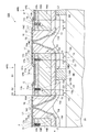
- FIG. 1 is a schematic perspective view showing a photodetecting device according to the present embodiment.
- FIG. 2 is a schematic plan view of the semiconductor photodetecting element.
- FIG. 3 is a schematic enlarged view of the semiconductor photodetector element.
- FIG. 4 is a diagram for explaining a cross-sectional configuration along the line IV-IV shown in FIG.
- the photodetection device 1 includes a semiconductor photodetection element 10A, a mounting substrate 20, and a glass substrate 30, as shown in FIG.
- the mounting substrate 20 faces the semiconductor photodetecting element 10A.
- the glass substrate 30 faces the semiconductor photodetecting element 10A.
- the semiconductor photodetecting element 10 ⁇ / b> A is disposed between the mounting substrate 20 and the glass substrate 30.
- a plane parallel to each main surface of the semiconductor photodetecting element 10A, the mounting substrate 20, and the glass substrate 30 is an XY axis plane, and a direction orthogonal to each main surface is a Z axis direction.
- the semiconductor photodetecting element 10A has a semiconductor substrate 50A having a rectangular shape in plan view.
- the semiconductor substrate 50A is made of Si and is an N-type (second conductivity type) semiconductor substrate.
- the semiconductor substrate 50A includes a main surface 1Na and a main surface 1Nb facing each other.
- the semiconductor photodetector element 10A includes a plurality of avalanche photodiodes APD and a plurality of through electrodes TE.
- the plurality of avalanche photodiodes APD are two-dimensionally arranged on the semiconductor substrate 50A.
- the plurality of avalanche photodiodes APD are arranged in a matrix.
- the row direction is the X-axis direction
- the column direction is the Y-axis direction.
- the avalanche photodiodes APD are arranged at equal intervals on a straight line when viewed from the X-axis direction and the Y-axis direction.
- Each avalanche photodiode APD has a light receiving region S1 and operates in Geiger mode.
- the light receiving region S1 is disposed on the main surface 1Na side of the semiconductor substrate 50A.
- each avalanche photodiode APD is connected in parallel with the quenching resistor R1 connected in series.
- a reverse bias voltage is applied from each power source to each avalanche photodiode APD.
- the output current from each avalanche photodiode APD is detected by the signal processing unit SP.
- the light receiving region S1 is a charge generation region (photosensitive region) where charge is generated according to incident light. That is, the light receiving area S1 is a light detection area.
- the glass substrate 30 has a main surface 30a and a main surface 30b facing each other.
- the glass substrate 30 has a rectangular shape in plan view.
- Main surface 30b is opposed to main surface 1Na of semiconductor substrate 50A.
- the main surface 30a and the main surface 30b are flat.
- the glass substrate 30 and the semiconductor photodetecting element 10A are optically connected by an optical adhesive OA.
- the glass substrate 30 may be directly formed on the semiconductor photodetecting element 10A.
- a scintillator (not shown) may be optically connected to the main surface 30a of the glass substrate 30.
- the scintillator is connected to the main surface 30a by an optical adhesive.
- the scintillation light from the scintillator passes through the glass substrate 30 and enters the semiconductor photodetecting element 10A.
- the mounting substrate 20 has a main surface 20a and a main surface 20b facing each other.
- the mounting substrate 20 has a rectangular shape in plan view.
- Main surface 20a is opposed to main surface 1Nb of semiconductor substrate 50A.
- the mounting substrate 20 includes a plurality of electrodes arranged on the main surface 20a. These electrodes are arranged corresponding to the through electrodes TE.
- the side surface 1Nc of the semiconductor substrate 50A, the side surface 30c of the glass substrate 30, and the side surface 20c of the mounting substrate 20 are flush with each other. That is, the outer edge of the semiconductor substrate 50 ⁇ / b> A, the outer edge of the glass substrate 30, and the outer edge of the mounting substrate 20 coincide with each other in plan view.
- the outer edge of the semiconductor substrate 50 ⁇ / b> A, the outer edge of the glass substrate 30, and the outer edge of the mounting substrate 20 may not coincide with each other.
- the area of the mounting substrate 20 may be larger than the areas of the semiconductor substrate 50A and the glass substrate 30 in plan view.
- the side surface 20c of the mounting substrate 20 is located outside the side surface 1Nc of the semiconductor substrate 50A and the side surface 30c of the glass substrate 30 in the XY axis plane direction.
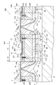
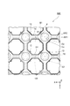
- FIG. 2 is a view of the semiconductor photodetector 10A as viewed from a direction (Z-axis direction) orthogonal to the main surface 1Na of the semiconductor substrate 50A.
- FIG. 3 shows a region where a groove is formed.
- One avalanche photodiode APD constitutes one cell in the semiconductor photodetecting element 10A.
- Each of the avalanche photodiodes APD has one light receiving region S1. That is, the semiconductor photodetecting element 10A has a plurality of light receiving regions S1.
- the light receiving region S1 has a polygonal shape when viewed from the Z-axis direction.
- the light receiving region S1 of the semiconductor photodetecting element 10A has a substantially regular octagonal shape when viewed from the Z-axis direction.
- the plurality of light receiving areas S1 are two-dimensionally arranged as viewed from the Z-axis direction.
- the plurality of light receiving regions S1 are arranged in a matrix.
- the light receiving regions S1 are arranged at equal intervals on a straight line when viewed from the X axis direction and the Y axis direction.
- the light receiving regions S1 are arranged at a pitch of 100 ⁇ m.
- two adjacent light receiving regions S1 are arranged so that one side of the octagonal shape faces each other.
- Each avalanche photodiode APD has an electrode E1.
- the electrode E1 is disposed on the main surface 1Na of the semiconductor substrate 50A.
- the electrode E1 is provided along the outline of the light receiving region S1, and has an octagonal ring shape.
- the electrode E1 has a connection portion C that is electrically connected to the light receiving region S1.
- the connection part C is provided on the four sides of the light receiving region S1.
- the connecting portions C are provided every other side of the light receiving region S1. In this case, the detection accuracy of the signal from the light receiving region S1 is ensured.
- the connection portion C includes a first end portion E1a and a second end portion E1b, and extends from the outer edge side of the light receiving region S1 toward the center side on the XY axis plane. ing.
- the electrode E1 extends in the Z-axis direction at the second end E1b. For this reason, a step is formed in the electrode E1 at the position of the second end E1b.
- the electrode E1 extends in the direction opposite to the center of the light receiving region S1 from the above-described step.
- the electrode E1 includes a third end E1c that is electrically connected to the wiring F.
- the wiring F extends from the third end E1c in the direction opposite to the center of the light receiving region S1.
- the wiring F electrically connects the electrode E1 and the electrode pad 12.
- the wiring F is located on the semiconductor substrate 50A outside the light receiving region S1.
- the wiring F is formed on the semiconductor substrate 50A via the insulating layer L1.
- the electrode E1 and the through electrode TE are made of metal.
- the electrode E1 and the through electrode TE are made of, for example, aluminum (Al).
- Al aluminum
- Cu copper
- the electrode E1 and the through electrode TE may be integrally formed.
- the electrode E1 and the through electrode TE are formed by, for example, a sputtering method.
- the semiconductor photodetecting element 10 ⁇ / b> A includes a plurality of through electrodes TE and a plurality of electrode pads 12. Each through electrode TE is electrically connected to the corresponding avalanche photodiode APD. Each electrode pad 12 is electrically connected to the corresponding through electrode TE. The electrode pad 12 is electrically connected to the electrode E1 through the wiring F. Electrode pad 12 is arranged on main surface 1Na. Each through electrode TE is electrically connected to the light receiving region S1 through the electrode pad 12, the wiring F, and the electrode E1. The electrode pad 12 is located in a region (inner region of the groove 13) AR1 surrounded by the groove 13 as viewed from the Z-axis direction, and is separated from the groove 13.
- the through electrode TE is disposed for each avalanche photodiode APD.
- the through electrode TE penetrates the semiconductor substrate 50A from the main surface 1Na side to the main surface 1Nb side.
- the through electrode TE is disposed in the through hole TH that penetrates the semiconductor substrate 50A in the thickness direction (Z-axis direction).
- the through hole TH is located in a region where a plurality of avalanche photodiodes APD are two-dimensionally arranged.
- a plurality of through holes TH are formed in the semiconductor substrate 50A.
- the opening of the through hole TH is located in the XY axis plane and has a circular shape when viewed from the Z axis direction.
- the cross-sectional shape of the through hole TH at a cutting plane parallel to the XY axis plane is a circular shape.
- the semiconductor photodetecting element 10A includes an insulating layer L2 on the inner peripheral surface of the through hole TH.
- the through electrode TE is disposed in the through hole TH via the insulating layer L2.
- the plurality of through holes TH are arranged so that the centers of the openings are located in a matrix when viewed from the Z-axis direction.
- the row direction is the X-axis direction
- the column direction is the Y-axis direction.
- the plurality of through holes TH are arranged such that the centers of the openings are arranged at equal intervals on a straight line when viewed from the X axis direction and the Y axis direction.
- the through holes TH are arranged at a pitch of 100 ⁇ m.
- the plurality of through holes TH are formed for each region surrounded by four adjacent avalanche photodiodes APD among the plurality of avalanche photodiodes APD.
- a through electrode TE electrically connected to the light receiving region S1 of one avalanche photodiode APD among the four adjacent avalanche photodiodes APD is disposed. That is, the through electrode TE is electrically connected to the light receiving region S1 of one avalanche photodiode APD among the four avalanche photodiodes APD surrounding the through hole TH in which the through electrode TE is disposed.
- the plurality of through-holes TH and the plurality of light-receiving regions S1 are configured such that the four through-holes TH surround one light-receiving region S1 and the four light-receiving regions S1 surround one through-hole TH when viewed from the Z-axis direction. positioned.
- the through holes TH and the light receiving regions S1 are alternately arranged in a direction intersecting the X axis and the Y axis.
- the four sides of the eight sides of the light receiving region S1 are opposed to one side of the adjacent light receiving region S1, and the remaining four sides are opposed to the adjacent through hole TH.
- One through hole TH is surrounded by one side of the four light receiving regions S1 when viewed from the Z-axis direction.
- the connection portion C is provided on four sides facing the through hole TH among the eight sides of the light receiving region S1.
- the main surface 1Na of the semiconductor substrate 50A includes a light receiving region S1, an intermediate region S2, and an opening peripheral region S3.
- the opening peripheral region S3 is a region located around the opening of the through hole TH of the main surface 1Na.
- the intermediate region S2 is a region on the main surface 1Na excluding the light receiving region S1 and the aperture peripheral region S3.
- a groove 13 is formed in the intermediate region S2 between the light receiving regions S1 of the four avalanche photodiodes APD adjacent to each other and the through holes TH surrounded by the avalanche photodiodes APD.
- the groove 13 extends along the side adjacent to the through hole TH among the plurality of sides of each light receiving region S1 of the four adjacent avalanche photodiodes APD as viewed from the Z-axis direction.
- the groove 13 surrounds the entire circumference of the through hole TH when viewed from the Z-axis direction.
- the area AR1 surrounded by the groove 13 is substantially square when viewed from the Z-axis direction.
- One through hole TH is formed in one region AR1.
- a groove 14 is formed in an intermediate region S2 between two light receiving regions S1 adjacent to each other.
- the groove 14 extends along two opposite sides of two adjacent light receiving regions S1 as viewed from the Z-axis direction.
- the groove 14 connects the grooves 13 surrounding different through holes TH.
- the semiconductor photodetecting element 10 ⁇ / b> A the entire circumference of the light receiving region S ⁇ b> 1 is surrounded by the grooves 13 and 14.
- One light receiving area S1 is arranged in one area AR2.
- the area AR2 has a substantially regular octagonal shape that is the same as the shape of the light receiving area S1.
- the areas AR1 and AR2 have a polygonal shape when viewed from the Z-axis direction.
- the groove 14 extends in a straight line in a region between two adjacent light receiving regions S1.
- the groove 14 surrounding the two adjacent light receiving regions S1 is shared by the two adjacent light receiving regions S1.
- the groove 14 located in a region between two adjacent light receiving regions S1 is a groove surrounding one light receiving region S1, and is also a groove surrounding the other light receiving region S1.
- the distance ⁇ from the edge 13e of the groove 13 to the edge D2 of the through hole TH surrounded by the groove 13 is equal to the distance 13f between the edge 13f of the groove 13 and the light receiving region S1 adjacent to the through hole TH. It is longer than the distance ⁇ to the edge D1.
- the distance ⁇ is 5.5 ⁇ m, and the distance ⁇ is 7.5 ⁇ m.
- the distance ⁇ is the shortest distance from the edge 13f of the groove 13 to the edge D1 of the light receiving region S1 adjacent to the through hole TH when viewed from the Z-axis direction.
- the distance ⁇ is the shortest distance from the edge 13e of the groove 13 to the edge D2 of the through hole TH surrounded by the groove 13 when viewed from the Z-axis direction.
- FIG. 4 a cross-sectional configuration of the semiconductor photodetecting element in the present embodiment will be described.
- illustration of the glass substrate 30 and the optical adhesive OA is omitted.
- Each avalanche photodiode APD includes a light receiving region S1.
- Each avalanche photodiode APD includes a P-type (first conductivity type) first semiconductor region 1PA, an N-type (second conductivity type) second semiconductor region 1NA, an N-type third semiconductor region 1NB, and P Type fourth semiconductor region 1PB.
- the first semiconductor region 1PA is located on the main surface 1Na side of the semiconductor substrate 50A.
- the second semiconductor region 1NA is located on the main surface 1Nb side of the semiconductor substrate 50A.
- the third semiconductor region 1NB is located between the first semiconductor region 1PA and the second semiconductor region 1NA, and has an impurity concentration lower than that of the second semiconductor region 1NA.
- the fourth semiconductor region 1PB is formed in the first semiconductor region 1PA and has an impurity concentration higher than that of the first semiconductor region 1PA.
- the fourth semiconductor region 1PB is the light receiving region S1.
- Each avalanche photodiode APD is from the main surface 1Na side, P + layer are quaternary semiconductor region 1PB, P layer is the first semiconductor region 1PA, N layer a third semiconductor region 1NB, the second semiconductor region 1NA It is constructed in the order of a certain N + layer.
- the first semiconductor region 1PA is located in the intermediate region S2 when viewed from the Z-axis direction, and is located so as to surround the fourth semiconductor region 1PB (light receiving region S1). Although not shown, the first semiconductor region 1PA is also located in the intermediate region S2 between the two light receiving regions S1 adjacent to each other when viewed from the Z-axis direction.
- the intermediate region S2 of the semiconductor substrate 50A has a P layer that is the first semiconductor region 1PA, an N layer that is the third semiconductor region 1NB, and a second semiconductor from the main surface 1Na side except the portion where the grooves 13 and 14 are formed.
- the region 1NA is configured in the order of N + layers.
- the inner surface 13b of the groove 13 is formed by the same N + layer as the second semiconductor region 1NA.
- An insulating layer 13c is provided on the inner surface 13b.
- a filler 13 a is disposed in the region surrounded by the insulating layer 13 c in the groove 13.
- the filler 13a is made of, for example, a material that can be easily filled and has high light shielding properties.
- the filler 13a is made of tungsten (W).
- the inner surface of the groove 14 is formed by the same N + layer as the second semiconductor region 1NA, like the inner surface 13b.
- an insulating layer 13 c and a filler 13 a are disposed in FIG. 4, the groove 14, the insulating layer 13 c and the filler 13 a disposed in the groove 14 are not illustrated.
- the filler 13a may be made of copper or aluminum instead of tungsten.
- the depth of the grooves 13 and 14, that is, the distance from the main surface 1Na to the bottom surface of the grooves 13 and 14 in the Z-axis direction (thickness direction of the semiconductor substrate 50A) is the second semiconductor from the main surface 1Na in the Z-axis direction. It is longer than the distance to the interface between the region 1NA and the third semiconductor region 1NB and shorter than the thickness of the semiconductor substrate 50A.
- the bottom surface 13d of the groove 13 is constituted by the second semiconductor region 1NA and is located closer to the main surface 1Nb than the third semiconductor region 1NB.
- the semiconductor substrate 50A has an N-type fifth semiconductor region 1NC.
- the fifth semiconductor region 1NC is formed between the edge D2 of the through hole TH and the first semiconductor region 1PA when viewed from the Z-axis direction.
- the fifth semiconductor region 1NC is an N + layer having a higher impurity concentration than the third semiconductor region 1NB, like the second semiconductor region 1NA.
- the region where the fifth semiconductor region 1NC is formed on the main surface 1Na is the opening peripheral region S3.
- the opening peripheral region S3 of the semiconductor substrate 50A is configured from the main surface 1Na side in the order of the N + layer as the fifth semiconductor region 1NC and the N + layer as the second semiconductor region 1NA.
- the inner peripheral surface (edge D2) of the through-hole TH is configured in order of the fifth semiconductor region 1NC and the second semiconductor region 1NA from the main surface 1Na side. Therefore, the PN junction formed by the first semiconductor region 1PA and the third semiconductor region 1NB is not exposed to the through hole TH.
- the avalanche photodiode APD has an electrode E1.
- the connection portion C of the electrode E1 is connected to the fourth semiconductor region 1PB (light receiving region S1). As described above, the connection portion C includes the first end portion E1a and the second end portion E1b.
- the electrode E1 includes a third end E1c.
- the first semiconductor region 1PA is electrically connected to the electrode E1 through the fourth semiconductor region 1PB.
- the electrode pad 12 is electrically connected to the through electrode TE.
- the through electrode TE extends to the back surface side (main surface 1Nb side) of the semiconductor substrate 50A.
- an insulating layer L3 is provided on the mounting substrate 20 side.
- the through electrode TE is electrically connected to the mounting substrate 20 through the bump electrode BE on the back surface side of the semiconductor substrate 50A.
- the electrode E1 and the mounting substrate 20 are electrically connected through the wiring F, the electrode pad 12, the through electrode TE, and the bump electrode BE.
- the fourth semiconductor region 1PB is electrically connected to the mounting substrate 20 through the electrode E1, the wiring F, the electrode pad 12, the through electrode TE, and the bump electrode BE.
- the bump electrode BE is made of, for example, solder.
- the bump electrode BE is formed on the through electrode TE extending on the main surface 1Nb via an unillustrated UBM (Under Bump Metal).
- the UBM is made of a material that is electrically and physically connected to the bump electrode BE.
- the UBM is formed by, for example, an electroless plating method.
- the bump electrode BE is formed by, for example, a method of mounting a solder ball or a printing method.
- FIG. 5 is a schematic plan view of the mounting substrate.
- the mounting substrate 20 includes a plurality of electrodes E9, a plurality of quenching resistors R1, and a plurality of signal processing units SP.
- the mounting board 20 constitutes an ASIC (Application Specific Integrated Circuit).
- the quenching resistor R1 may be arranged not on the mounting substrate 20 but on the semiconductor photodetecting element 10A.
- Each electrode E9 is electrically connected to the bump electrode BE. Similarly to the electrode E1 and the through electrode TE, the electrode E9 is made of metal.
- the electrode E9 is made of, for example, aluminum.
- the material constituting the electrode E9 may be copper other than aluminum.
- Each quenching resistor R1 is arranged on the main surface 20a side. One end of the quenching resistor R1 is electrically connected to the electrode E9, and the other end of the quenching resistor R1 is connected to the common electrode CE.
- the quenching resistor R1 constitutes a passive quenching circuit. A plurality of quenching resistors R1 are connected in parallel to the common electrode CE.
- Each signal processing unit SP is arranged on the main surface 20a side. The input end of the signal processing unit SP is electrically connected to the electrode E9, and the output end of the signal processing unit SP is connected to the signal line TL. An output signal from the corresponding avalanche photodiode APD (semiconductor photodetecting element 10A) is input to each signal processing unit SP through the electrode E1, the through electrode TE, the bump electrode BE, and the electrode E9. Each signal processing unit SP processes an output signal from the corresponding avalanche photodiode APD. Each signal processing unit SP includes a CMOS circuit that converts an output signal from the corresponding avalanche photodiode APD into a digital pulse.
- CMOS circuit that converts an output signal from the corresponding avalanche photodiode APD into a digital pulse.
- FIG. 6 is a circuit diagram of the photodetector.
- an avalanche photodiode APD is formed by a PN junction formed between the N-type third semiconductor region 1NB and the P-type first semiconductor region 1PA. Yes.
- the semiconductor substrate 50A is electrically connected to an electrode (not shown) arranged on the back side, and the first semiconductor region 1PA is connected to the electrode E1 through the fourth semiconductor region 1PB.
- Each quenching resistor R1 is connected in series with a corresponding avalanche photodiode APD.
- each avalanche photodiode APD operates in Geiger mode.
- a reverse voltage (reverse bias voltage) larger than the breakdown voltage of the avalanche photodiode APD is applied between the anode and the cathode of the avalanche photodiode APD.
- the ( ⁇ ) potential V1 is applied to the anode
- the (+) potential V2 is applied to the cathode.
- the polarities of these potentials are relative, and one potential may be a ground potential.
- the anode is the first semiconductor region 1PA, and the cathode is the third semiconductor region 1NB.
- photoelectric conversion is performed inside the substrate to generate photoelectrons.
- Avalanche multiplication is performed in a region near the PN junction interface of the first semiconductor region 1PA, and the amplified electron group travels toward an electrode disposed on the back surface side of the semiconductor substrate 50A.
- light (photon) enters one of the cells (avalanche photodiode APD) of the semiconductor photodetecting element 10A it is multiplied and taken out from the electrode E9 as a signal.
- the signal extracted from the electrode E9 is input to the corresponding signal processing unit SP.
- the groove 13 surrounding the through hole TH on the main surface 1Na side of the semiconductor substrate 50A is an intermediate between the through hole TH and the light receiving region S1 adjacent to the through hole TH. It is formed in region S2. For this reason, the main surface 1Na of the semiconductor substrate 50A is divided in the intermediate region S2 between the through electrode TE and the light receiving region S1. As a result, even when the light receiving region S1 and the through electrode TE are close to each other in order to ensure the aperture ratio of the avalanche photodiode APD, the flow of surface leakage current from the through electrode TE to the avalanche photodiode APD is reduced. .
- the distance ⁇ is longer than the distance ⁇ . For this reason, a structural defect hardly occurs around the through hole TH in the semiconductor substrate 50A.
- the bottom surface 13d of the groove 13 is constituted by the second semiconductor region 1NA.
- the bottom surface 13d of the groove 13 is deeper than the third semiconductor region 1NB. For this reason, when a charge is generated in a region surrounded by the groove 13 in the semiconductor substrate 50A, the charge generated in the region is suppressed from moving to the avalanche photodiode APD. Since the bottom surface 13d of the groove 13 is formed in the semiconductor substrate 50A, that is, the groove 13 does not reach the main surface 1Nb of the semiconductor substrate 50A, there is no possibility that the semiconductor substrate 50A is separated at the position of the groove 13. Therefore, in the manufacturing process of the photodetecting device 1, the semiconductor substrate 50A can be easily handled.
- a filler 13a made of tungsten is arranged in the groove 13. Since the electrode pad 12 is separated from the groove 13, the parasitic capacitance generated between the electrode pad 12 and the filler 13a is reduced.
- the region AR1 and the region AR2 When viewed from the Z-axis direction, the region AR1 and the region AR2 have a polygonal shape, and the light receiving region S1 has a polygonal shape.
- the light receiving region S1 When the light receiving region S1 is circular, there is no corner where the electric field concentrates.
- the light receiving region S1 has a circular shape, the dead space generated between the light receiving region S1 and the through hole TH is larger than when the light receiving region S1 has a polygonal shape.
- the areas AR1 and AR2 and the light receiving area S1 are polygonal shapes.
- the regions AR1, AR2 and the light receiving region S1 are arranged so that the sides of the regions AR1, AR2 and the side of the light receiving region S1 are along. For this reason, in the photodetection device 1, the dead space is small and the aperture ratio is large.
- the opening of the through hole TH has a circular shape, and the insulating layer L2 is disposed on the inner peripheral surface of the through hole TH.
- the through electrode TE and the semiconductor substrate 50A are electrically insulated. If corners exist in the openings of the through holes TH, when the insulating layer L2 is formed, the insulating layer L2 formed at the corners may be cracked.
- the through hole TH since the through hole TH has a circular shape when viewed from the direction orthogonal to the main surface 1Na, the insulating layer L2 is unlikely to crack when the insulating layer L2 is formed. Therefore, in the photodetector 1, electrical insulation between the through electrode TE and the semiconductor substrate 50A is ensured.
- the through electrode TE is electrically connected to the light receiving region S1 of one avalanche photodiode APD among the four adjacent avalanche photodiodes APD.
- the wiring distance between the through electrode TE and the light receiving region S1 electrically connected to the through electrode TE is relatively short, the wiring resistance and the parasitic capacitance are hardly affected. Therefore, deterioration of detection accuracy in the light detection device 1 is suppressed.
- the light receiving region S1 has a polygonal shape when viewed from the Z-axis direction.
- the groove 13 extends along the side adjacent to the through hole TH among the plurality of sides of each of the light receiving regions S1 of the four avalanche photodiodes APD adjacent to the through hole TH when viewed from the Z-axis direction. Yes. Since the groove 13 extends along the side of the light receiving region S1, even when the through hole TH is formed in each region surrounded by four adjacent avalanche photodiodes APD, It is possible to set the interval with the region S1 narrow. Therefore, in the photodetecting device 1, the dead space is small and the aperture ratio is large.
- the light receiving region S1 has an octagonal shape when viewed from the Z-axis direction, it is possible to effectively utilize a region other than the through electrode TE in the main surface 1Na. Accordingly, in the light detection device 1, a configuration in which the wiring distance between the through electrode TE and the light receiving region S1 is short is realized, and the aperture ratio is higher than that in the case where the light receiving region S1 has another shape. improves.
- the filler 13a disposed in the grooves 13 and 14 is made of metal, a parasitic capacitance may be generated between the filler 13a and the light receiving region S1. If the value of the parasitic capacitance differs depending on the position between the filler 13a and the light receiving region S1, that is, if the parasitic capacitance value is biased, the light detection accuracy of the avalanche photodiode APD decreases. There is a fear.
- the grooves 13 and 14 are formed so that the edges of the grooves 13 and 14 are along the edge D1 of the light receiving region S1 when viewed from the Z-axis direction.
- the groove 14 surrounding two adjacent light receiving regions S1 is formed so that the edge of the groove 14 is along the edge D1 of the light receiving region S1.
- the groove 14 is shared by two adjacent light receiving regions S1. For this reason, the influence of the parasitic capacitance on the avalanche photodiode APD is reduced. Further, since the area of the main surface 1Na is effectively used, the light receiving areas S1 of the avalanche photodiodes APD are densely arranged. As a result, both reduction of the influence of parasitic capacitance on the avalanche photodiode APD and improvement of the aperture ratio are compatible.
- FIG. 7 is a diagram for explaining a cross-sectional configuration of a photodetection device according to a modification of the present embodiment.
- FIG. 7 shows a cross-sectional configuration when the photodetecting device according to the present modification is cut along a plane corresponding to line IV-IV shown in FIG. Also in FIG. 7, illustration of the glass substrate 30 and the optical adhesive OA is omitted.
- This modification is generally similar to or the same as the above-described embodiment, but as described below, this modification is different from the above-described embodiment with respect to the configuration of the avalanche photodiode APD.
- the light detection device includes a semiconductor light detection element 10B.
- the semiconductor photodetecting element 10 ⁇ / b> B is disposed between the mounting substrate 20 and the glass substrate 30.
- the semiconductor photodetecting element 10B has a semiconductor substrate 50B that has a rectangular shape in plan view.
- the semiconductor substrate 50B is made of Si and is an N-type (second conductivity type) semiconductor substrate.
- Semiconductor substrate 50B includes a main surface 1Na and a main surface 1Nb facing each other.
- the semiconductor photodetecting element 10B includes a plurality of avalanche photodiodes APD and a plurality of through electrodes TE.
- the plurality of avalanche photodiodes APD are two-dimensionally arranged on the semiconductor substrate 50B. In this modification, the plurality of avalanche photodiodes APD are arranged in a matrix.
- the groove 23 formed in the semiconductor light detection element 10B has the same configuration as the groove 13 formed in the semiconductor light detection element 10A.
- the groove 23 is formed in an intermediate region S2 between the light receiving regions S1 of the four adjacent avalanche photodiodes APD and the through holes TH surrounded by the avalanche photodiodes APD.
- the groove 23 extends along the side adjacent to the through hole TH among the plurality of sides of each light receiving region S1 of the four avalanche photodiodes APD adjacent to the through hole TH when viewed from the Z-axis direction. .
- the groove 23 surrounds the entire circumference of the through hole TH.
- the area AR1 surrounded by the groove 23 is substantially square when viewed from the Z-axis direction.
- one through hole TH is formed in one region AR1.
- a groove 14 is formed in an intermediate region S2 between two light receiving regions S1 adjacent to each other. In FIG. 7, the groove 14 is not shown. The groove 14 extends along two opposite sides of two adjacent light receiving regions S1 when viewed from the Z direction. The groove 14 connects the grooves 23 surrounding different through holes TH. Also in the semiconductor light detection element 10B, the entire circumference of the light receiving region S1 is surrounded by the grooves 23 and 14. The area AR2 surrounded by the grooves 23 and 14 has a substantially regular octagonal shape that is the same as the shape of the light receiving area S1. Also in this modification, the areas AR1 and AR2 have a polygonal shape when viewed from the Z-axis direction. One light receiving area S1 is arranged in one area AR2.
- the groove 14 extends in a straight line in a region between two adjacent light receiving regions S1.
- the groove 14 surrounding the two adjacent light receiving regions S1 is shared by the two adjacent light receiving regions S1.
- the distance ⁇ from the edge 23e of the groove 23 to the edge D2 of the through hole TH surrounded by the groove 23 is the edge of the light receiving region S1 adjacent to the through hole TH from the edge 23f of the groove 23. It is longer than the distance ⁇ to D1.
- the distance ⁇ is 5.5 ⁇ m and the distance ⁇ is 7.5 ⁇ m.
- the distance ⁇ is the shortest distance from the edge 23f of the groove 23 to the edge D1 of the light receiving region S1 adjacent to the through hole TH when viewed from the Z-axis direction.
- the distance ⁇ is the shortest distance from the edge 23e of the groove 23 to the edge D2 of the through hole TH surrounded by the groove 23 when viewed from the Z-axis direction.
- each avalanche photodiode APD includes a light receiving region S1.
- Each avalanche photodiode APD includes a P-type (first conductivity type) first semiconductor region 2PA, a P-type second semiconductor region 2PB, an N-type third semiconductor region 2NA, and a P-type fourth semiconductor region. 2PC.
- the first semiconductor region 2PA is located on the main surface 1Na side of the semiconductor substrate 50B.
- the second semiconductor region 2PB is located on the main surface 1Nb side of the semiconductor substrate 50B and has a higher impurity concentration than the first semiconductor region 2PA.
- the third semiconductor region 2NA is formed on the main surface 1Na side of the first semiconductor region 2PA.
- the fourth semiconductor region 2PC is formed in the first semiconductor region 2PA so as to be in contact with the third semiconductor region 2NA, and has an impurity concentration higher than that of the first semiconductor region 2PA.
- the third semiconductor region 2NA is the light receiving region S1.
- Each avalanche photodiode APD is from the main surface 1Na side, N + layer a third semiconductor region 2NA, P layer are quaternary semiconductor region 2PC, a first semiconductor region 2PA P - layer, the second semiconductor region 2PB In the order of the P + layers.
- the first semiconductor region 2PA is located in the intermediate region S2 when viewed from the Z-axis direction, and is located so as to surround the third semiconductor region 2NA that is the light receiving region S1. Although not shown, the first semiconductor region 2PA is also located in the intermediate region S2 between the two light receiving regions S1 adjacent to each other when viewed from the Z-axis direction.
- the intermediate region S2 of the semiconductor substrate 50B is in the order of the P ⁇ layer that is the first semiconductor region 2PA and the P + layer that is the second semiconductor region 2PB from the main surface 1Na side except the portion where the grooves 23 and 14 are formed. It consists of
- the inner surface 23b of the groove 23 is formed by the same P + layer as that of the second semiconductor region 2PB.
- An insulating layer 23c is provided on the inner surface 23b.
- a filler 23a is disposed in the region surrounded by the insulating layer 23c in the groove 23.
- the filler 23a is made of, for example, a material that can be easily filled and has high light shielding properties.
- the filler 23a is made of tungsten (W), like the filler 13a.
- the inner surface of the groove 14 is formed by a P + layer having a higher impurity concentration than the first semiconductor region 2PA.
- an insulating layer 23 c and a filler 23 a are disposed in the groove 14. In FIG. 7, as described above, the groove 14 and the insulating layer 23c and the filler 23a disposed in the groove 14 are not illustrated.
- the filler 13a may be made of copper or aluminum instead of tungsten.
- the depth of the grooves 23, 14, that is, the distance from the main surface 1 Na in the Z-axis direction (the thickness direction of the semiconductor substrate 50 B) to the bottom surfaces of the grooves 23, 14 is the main surface 1 Na in the Z-axis direction to the first semiconductor. It is longer than the distance to the interface between the region 2PA and the second semiconductor region 2PB and shorter than the thickness of the semiconductor substrate 50B.
- the bottom surface 23d of the groove 23 is configured by the second semiconductor region 2PB, and is located closer to the main surface 1Nb than the first semiconductor region 2PA.
- the semiconductor substrate 50B has a P-type fifth semiconductor region 2PD.
- the fifth semiconductor region 2PD is formed between the edge D2 of the through hole TH and the first semiconductor region 2PA when viewed from the Z-axis direction.
- the fifth semiconductor region 2PD is a P + layer having a higher impurity concentration than the first semiconductor region 2PA, like the second semiconductor region 2PB.
- a region where the fifth semiconductor region 2PD is formed in the main surface 1Na is the opening peripheral region S3.
- the opening peripheral region S3 of the semiconductor substrate 50B is configured from the main surface 1Na side in the order of the P + layer that is the fifth semiconductor region 2PD and the P + layer that is the second semiconductor region 2PB.
- the inner peripheral surface (edge D2) of the through hole TH is configured in order of the fifth semiconductor region 2PD and the second semiconductor region 2PB from the main surface 1Na side. Therefore, the PN junction formed by the third semiconductor region 2NA and the fourth semiconductor region 2PC is not exposed to the through hole TH.
- the avalanche photodiode APD has an electrode E1.
- the electrode E1 is disposed on the main surface 1Na side of the semiconductor substrate 50B. Also in this modification, the electrode E1 is provided along the outline of the light receiving region S1 and has an octagonal ring shape.
- the electrode E1 has a connection portion C that is electrically connected to the light receiving region S1. Also in this modification, as FIG. 7 shows, the connection part C contains the 1st end part E1a and the 2nd end part E1b. The electrode E1 includes a third end E1c that is electrically connected to the wiring F.
- the wiring F extends from the third end E1c in the direction opposite to the center of the light receiving region S1.
- the wiring F electrically connects the electrode E1 and the electrode pad 12.
- the wiring F is located on the semiconductor substrate 50B outside the light receiving region S1.
- the wiring F is formed on the semiconductor substrate 50B via the insulating layer L1.
- the electrode pad 12 is electrically connected to the through electrode TE.
- the through electrode TE extends to the back surface side (main surface 1Nb side) of the semiconductor substrate 50B.
- the through electrode TE is provided with an insulating layer L3.
- the through electrode TE is electrically connected to the mounting substrate 20 by the bump electrode BE.
- the electrode E1 and the mounting substrate 20 are electrically connected through the wiring F, the electrode pad 12, the through electrode TE, and the bump electrode BE.
- the third semiconductor region 2NA is electrically connected to the mounting substrate 20 through the electrode E1, the wiring F, the electrode pad 12, the through electrode TE, and the bump electrode BE.
- the groove 23 surrounding the through hole TH on the main surface 1Na side of the semiconductor substrate 50B is an intermediate between the through hole TH and the light receiving region S1 adjacent to the through hole TH. It is formed in region S2. For this reason, the main surface 1Na of the semiconductor substrate 50B is divided in the intermediate region S2 between the through electrode TE and the light receiving region S1. As a result, even when the light receiving region S1 and the through electrode TE are close to each other in order to ensure the aperture ratio of the avalanche photodiode APD, the flow of surface leakage current from the through electrode TE to the avalanche photodiode APD is reduced. .
- the distance ⁇ is longer than the distance ⁇ . For this reason, a structural defect hardly occurs around the through hole TH in the semiconductor substrate 50B.
- the bottom surface 23d of the groove 23 is constituted by the second semiconductor region 2PB.
- the bottom surface 23d of the groove 23 is deeper than the first semiconductor region 2PA. For this reason, when a charge is generated in a region surrounded by the groove 23 in the semiconductor substrate 50B, the charge generated in the region is suppressed from moving to the avalanche photodiode APD. Since the bottom surface 23d of the groove 23 is formed in the semiconductor substrate 50B, that is, the groove 23 does not reach the main surface 1Nb of the semiconductor substrate 50B, there is no possibility that the semiconductor substrate 50B is separated at the position of the groove 23. Therefore, it is easy to handle the semiconductor substrate 50B even in the manufacturing process of the photodetector according to this modification.
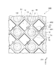
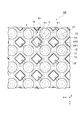
- FIGS. 8 to 11 are schematic plan views showing modified examples of the semiconductor photodetecting element.
- the semiconductor photodetecting elements 10C, 10D, 10E, and 10F are disposed between the mounting substrate 20 and the glass substrate 30.
- the semiconductor photodetecting elements 10C, 10D, 10E, and 10F have a semiconductor substrate 50A that has a rectangular shape in plan view, like the semiconductor photodetecting element 10A.
- the semiconductor photodetecting elements 10C, 10D, 10E, and 10F include a plurality of avalanche photodiodes APD and a plurality of through electrodes TE.
- a groove 13 is formed in an intermediate region S2 between the through hole TH and the light receiving region S1 adjacent to the through hole TH.
- the groove 13 surrounds the through hole TH.
- the groove 13 is not formed in a region where the wiring F that electrically connects the through electrode TE and the light receiving region S1 is disposed as viewed from the Z-axis direction.
- the groove 13 surrounds the through hole TH in a state where the groove 13 is divided in a region where the wiring F is disposed as viewed from the Z-axis direction.
- a groove 13 is formed in an intermediate region S2 between the through hole TH and the light receiving region S1 adjacent to the through hole TH.
- the groove 13 surrounds the through hole TH.
- FIG. 2 and FIG. 9 are different in scale.
- the size of the electrode pad 12 of the semiconductor photodetecting element 10D is the same as the size of the electrode pad 12 of the semiconductor photodetecting element 10A.
- the through holes TH and the light receiving areas S1 are two-dimensionally arranged. Each pitch of the through hole TH and the light receiving region S1 is smaller than that of the semiconductor photodetector 10A. In the semiconductor photodetector 10D, the through holes TH and the light receiving regions S1 are arranged in a one-to-one relationship so that the resolution is higher than that of the semiconductor photodetector 10A. Each pitch of the light receiving region S1 and the through holes TH is, for example, 70 ⁇ m.
- the groove 13 surrounds the through hole TH, similarly to the semiconductor photodetecting element 10A.
- the groove 14 also extends along two opposite sides of the two adjacent light receiving regions S1 when viewed from the Z-axis direction.
- the groove 14 connects the grooves 13 surrounding different through holes TH.
- the entire circumference of the light receiving region S1 is surrounded by the grooves 13 and 14.
- each pitch of the through electrode TE and the light receiving region S1 is smaller than that of the semiconductor photodetecting element 10A.
- the groove 14 surrounding the two adjacent light receiving regions S1 is formed so that the edge of the groove 14 is along the edge D1 of the light receiving region S1. .
- the groove 14 is shared by two adjacent light receiving regions S1. For this reason, the influence of the parasitic capacitance on the avalanche photodiode APD is reduced. Further, since the area of the main surface 1Na is effectively used, the light receiving areas S1 of the avalanche photodiodes APD are densely arranged.
- the light receiving region S1 has a polygonal shape.
- the light receiving region S1 of the semiconductor light detecting element 10D has a polygonal shape different from that of the light receiving region S1 of the semiconductor light detecting element 10A. Specifically, the light receiving region S1 of the semiconductor photodetector 10D has a polygonal shape in which the length of the side facing the adjacent light receiving region S1 is shorter than the length of the side facing the adjacent through hole TH. Yes.
- the semiconductor light detection element 10D has a higher resolution and a higher aperture ratio than the semiconductor light detection element 10A. Parasitic capacitance generated among the avalanche photodiode APD, the filler 13a, and the electrode pad 12 is reduced.
- a groove 13 is formed in an intermediate region S2 between the through hole TH and the light receiving region S1 adjacent to the through hole TH.
- the groove 13 surrounds the through hole TH. 2 and FIG. 10 are different in scale.
- the size of the electrode pad 12 of the semiconductor photodetecting element 10E is the same as the size of the electrode pad 12 of the semiconductor photodetecting element 10A.
- the pitch of the through holes TH is the same as the pitch of the through holes TH of the semiconductor photodetector 10A
- the pitch of the light receiving regions S1 is the same as the pitch of the light receiving regions S1 of the semiconductor photodetector 10A.
- the through hole TH and the light receiving region S1 are arranged in a one-to-one relationship between the through hole TH and the light receiving region S1.
- the light receiving region S1 of the semiconductor light detecting element 10E has a substantially octagonal shape, similar to the light receiving region S1 of the semiconductor light detecting element 10A.
- the area of the light receiving region S1 of the semiconductor photodetector 10E is smaller than the area of the light receiving region S1 of the semiconductor photodetector 10A.
- two grooves 14 extend in a region between two light receiving regions S1 adjacent to each other.
- One groove 14 surrounds one light receiving region S1, and the other groove 14 surrounds the other light receiving region S1. That is, the groove 14 is not shared for two adjacent light receiving regions S1.
- the groove 13 of the semiconductor photodetecting element 10E surrounds the through hole TH in a state of being divided in the row direction and the column direction in which the through holes TH are arranged. Similar to the groove 14 of the semiconductor light detection element 10A, the groove 14 of the semiconductor light detection element 10E extends along opposite sides of the two adjacent light receiving regions S1 when viewed from the Z-axis direction. The groove 14 connects the grooves 13 surrounding different through holes TH. In the semiconductor photodetecting element 10E, the entire circumference of the light receiving region S1 is surrounded by the grooves 13 and 14.
- the grooves 13 and 14 are formed so that the edges of the grooves 13 and 14 are along the edge D1 of the light receiving region S1. It is difficult to reduce the size of the through electrode TE in order to ensure processing accuracy or ensure electrical connection. In order to reduce the parasitic capacitance generated between the electrode pad 12 and the filler 13 a disposed in the grooves 13 and 14, the grooves 13 and 14 are separated from the electrode pad 12.
- the semiconductor photodetecting element 10E since the two grooves 14 extend in the area between the two light receiving areas S1 adjacent to each other, the crosstalk between the light receiving areas S1 is reduced as compared with the semiconductor photodetecting element 10A. The Therefore, in the semiconductor photodetecting element 10E, the crosstalk between the light receiving regions S1 is reduced as compared with the semiconductor photodetecting element 10A, and the parasitic capacitance generated between the avalanche photodiode APD, the filler 13a, and the electrode pad 12 is reduced. Reduced.
- a groove 13 is formed in an intermediate region S2 between the through hole TH and the light receiving region S1 adjacent to the through hole TH.
- the groove 13 surrounds the through hole TH.
- FIG. 10 and FIG. 11 are different in scale.
- the size of the electrode pad 12 of the semiconductor photodetecting element 10F is the same as the size of the electrode pad 12 of the semiconductor photodetecting element 10E.
- the through holes TH and the light receiving areas S1 are two-dimensionally arranged. Each pitch of the through hole TH and the light receiving region S1 is smaller than that of the semiconductor photodetector 10E.
- the through holes TH and the light receiving regions S1 are arranged in a one-to-one relationship so that the resolution is higher than that of the semiconductor light detection element 10E.
- Each pitch of the light receiving region S1 and the through holes TH is, for example, 50 ⁇ m.
- the groove 13 of the semiconductor photodetecting element 10F surrounds the through hole TH in a state of being divided in the row direction and the column direction in which the through holes TH are arranged. Similar to the groove 14 of the semiconductor light detection element 10E, the groove 14 of the semiconductor light detection element 10F extends along the mutually opposing sides of the two adjacent light receiving regions S1 as viewed from the Z-axis direction. The groove 14 connects the grooves 13 surrounding different through holes TH. In the semiconductor photodetecting element 10F, the entire circumference of the light receiving region S1 is surrounded by the grooves 13 and 14.
- the grooves 13 and 14 are formed so that the edges of the grooves 13 and 14 are along the edge D1 of the light receiving region S1. It is difficult to reduce the size of the through electrode TE in order to ensure processing accuracy or ensure electrical connection. In order to reduce the parasitic capacitance generated between the electrode pad 12 and the filler 13 a disposed in the grooves 13 and 14, the grooves 13 and 14 are separated from the electrode pad 12.
- the groove 14 is not shared by two adjacent light receiving regions S1, and the light receiving region S1 of the semiconductor photodetector 10F has a shape different from that of the light receiving region S1 of the semiconductor photodetector 10E. It has a polygonal shape. Specifically, the light receiving region S1 of the semiconductor photodetector 10F has a polygonal shape in which the length of the side facing the adjacent light receiving region S1 is shorter than the length of the side facing the adjacent through hole TH. Yes.
- the semiconductor photodetecting element 10F has higher resolution than the semiconductor photodetecting element 10E, and an aperture ratio is ensured. Parasitic capacitance generated among the avalanche photodiode APD, the filler 13a, and the electrode pad 12 is reduced.
- one avalanche photodiode APD is electrically connected to one through electrode TE (one electrode pad 12), but the present invention is not limited to this.
- a plurality of avalanche photodiodes APD may be electrically connected to one through electrode TE (one electrode pad 12).
- the two-layer structure of the semiconductor substrate 50A and the semiconductor substrate 50B is shown for the avalanche photodiode APD, but the layer structure of the semiconductor substrate is not limited to these.
- the avalanche photodiode APD provided on the semiconductor substrate 50A for example, the second semiconductor region 1NA and the third semiconductor region 1NB may be configured by one semiconductor region.
- the avalanche photodiode APD includes a first conductivity type (for example, N type) semiconductor region and a second conductivity type (for example, P type) semiconductor region that forms a pn junction with the first conductivity type semiconductor region.
- the second conductivity type semiconductor region having a higher impurity concentration is the light receiving region.
- the first semiconductor region 2PA, the second semiconductor region 2PB, and the fourth semiconductor region 2PC may be configured by one semiconductor region.
- the avalanche photodiode APD is located in the first conductivity type (for example, P type) semiconductor region, the first conductivity type semiconductor region, and has a pn junction with the first conductivity type semiconductor region.
- the P-type and N-type conductivity types may be switched so as to be opposite to the above-described conductivity types.
- the light receiving region S1 of the semiconductor substrate 50A may be configured in the order of the N + layer, the N layer, the P layer, and the P + layer from the main surface 1Na side.
- the light receiving region S1 of the semiconductor substrate 50B may be configured in the order of the P + layer, the N layer, the N ⁇ layer, and the N + layer from the main surface 1Na side.
- the distance ⁇ is 5.5 ⁇ m, and the distance ⁇ is 7.5 ⁇ m.
- the distance ⁇ and the distance ⁇ may be other than the above values as long as the distance ⁇ is longer than the distance ⁇ .
- the light receiving region S1 is described as having a polygonal shape (for example, a substantially regular octagonal shape) when viewed from the Z-axis direction, but other shapes may be used. .
- the light receiving region S1 may have a circular shape or any other appropriate shape.
- the through hole TH has been described as having a circular shape when viewed from the Z-axis direction, but other shapes may be used.
- the through hole TH may have a polygonal shape or any other appropriate shape.
- the present invention can be used for a light detection device that detects weak light.
- SYMBOLS 1 Photodetection device, 12 ... Electrode pad, 13, 23 ... Groove, 13d, 23d ... Bottom, 50A, 50B ... Semiconductor substrate, 1Na, 1Nb ... Main surface, S1 ... Light receiving region, S2 ... Intermediate region, APD ... Avalanche Photodiode, TH ... through hole, TE ... through electrode, ⁇ , ⁇ ... distance, 1PA ... first semiconductor region, 1PB ... fourth semiconductor region, 1NA ... second semiconductor region, 1NB ... third semiconductor region, 2PA ... first One semiconductor region, 2PB ... second semiconductor region, 2PC ... fourth semiconductor region, 2NA ... third semiconductor region, AR1, AR2 ... region, D1, D2, 13e, 13f ... edge.
Landscapes
- Physics & Mathematics (AREA)
- Engineering & Computer Science (AREA)
- Power Engineering (AREA)
- Condensed Matter Physics & Semiconductors (AREA)
- General Physics & Mathematics (AREA)
- Computer Hardware Design (AREA)
- Microelectronics & Electronic Packaging (AREA)
- Electromagnetism (AREA)
- Health & Medical Sciences (AREA)
- Toxicology (AREA)
- Light Receiving Elements (AREA)
- Solid State Image Pick-Up Elements (AREA)
Priority Applications (6)
| Application Number | Priority Date | Filing Date | Title |
|---|---|---|---|
| JP2018530356A JP6839713B2 (ja) | 2016-07-27 | 2017-07-26 | 光検出装置 |
| US16/315,708 US10658415B2 (en) | 2016-07-27 | 2017-07-26 | Light detection device |
| CN201780046066.6A CN109564953B (zh) | 2016-07-27 | 2017-07-26 | 光检测装置 |
| EP17834415.6A EP3493276B1 (en) | 2016-07-27 | 2017-07-26 | Light detection device |
| US16/834,121 US11362127B2 (en) | 2016-07-27 | 2020-03-30 | Light detection device |
| US17/714,904 US20220231071A1 (en) | 2016-07-27 | 2022-04-06 | Light detection device |
Applications Claiming Priority (2)
| Application Number | Priority Date | Filing Date | Title |
|---|---|---|---|
| JP2016147378 | 2016-07-27 | ||
| JP2016-147378 | 2016-07-27 |
Related Child Applications (2)
| Application Number | Title | Priority Date | Filing Date |
|---|---|---|---|
| US16/315,708 A-371-Of-International US10658415B2 (en) | 2016-07-27 | 2017-07-26 | Light detection device |
| US16/834,121 Continuation US11362127B2 (en) | 2016-07-27 | 2020-03-30 | Light detection device |
Publications (1)
| Publication Number | Publication Date |
|---|---|
| WO2018021413A1 true WO2018021413A1 (ja) | 2018-02-01 |
Family
ID=61016014
Family Applications (1)
| Application Number | Title | Priority Date | Filing Date |
|---|---|---|---|
| PCT/JP2017/027057 WO2018021413A1 (ja) | 2016-07-27 | 2017-07-26 | 光検出装置 |
Country Status (5)
| Country | Link |
|---|---|
| US (3) | US10658415B2 (zh) |
| EP (1) | EP3493276B1 (zh) |
| JP (1) | JP6839713B2 (zh) |
| CN (1) | CN109564953B (zh) |
| WO (1) | WO2018021413A1 (zh) |
Cited By (4)
| Publication number | Priority date | Publication date | Assignee | Title |
|---|---|---|---|---|
| CN111766592A (zh) * | 2019-03-13 | 2020-10-13 | 株式会社东芝 | 传感器以及距离测量装置 |
| CN112424634A (zh) * | 2018-07-18 | 2021-02-26 | 浜松光子学株式会社 | 半导体光检测装置 |
| JP2021072347A (ja) * | 2019-10-30 | 2021-05-06 | 株式会社東芝 | 光検出器、光検出システム、ライダー装置、及び車 |
| WO2022113515A1 (ja) * | 2020-11-24 | 2022-06-02 | ソニーセミコンダクタソリューションズ株式会社 | センサデバイス |
Families Citing this family (3)
| Publication number | Priority date | Publication date | Assignee | Title |
|---|---|---|---|---|
| USD994512S1 (en) * | 2021-11-01 | 2023-08-08 | SimpliSafe, Inc. | Infrared sensor |
| USD994513S1 (en) * | 2021-11-01 | 2023-08-08 | SimpliSafe, Inc. | Infrared sensor |
| USD993049S1 (en) * | 2021-11-01 | 2023-07-25 | SimpliSafe, Inc. | Infrared sensor |
Citations (7)
| Publication number | Priority date | Publication date | Assignee | Title |
|---|---|---|---|---|
| JP2009065200A (ja) * | 2008-11-18 | 2009-03-26 | Hamamatsu Photonics Kk | 放射線検出器 |
| JP2010153603A (ja) * | 2008-12-25 | 2010-07-08 | Fujifilm Corp | 固体撮像装置 |
| US20110272561A1 (en) * | 2010-03-23 | 2011-11-10 | Stmicroelectronics S.R.L. | Method of detecting impinging position of photons on a geiger-mode avalanche photodiode, related geiger-mode avalanche photodiode and fabrication process |
| JP2012124484A (ja) * | 2010-12-07 | 2012-06-28 | Imec | 分離トレンチの形成方法 |
| WO2015025723A1 (ja) * | 2013-08-19 | 2015-02-26 | ソニー株式会社 | 固体撮像素子および電子機器 |
| JP2015061041A (ja) | 2013-09-20 | 2015-03-30 | 株式会社東芝 | 放射線検出器および放射線検出装置 |
| JP2016029738A (ja) * | 2015-10-28 | 2016-03-03 | 浜松ホトニクス株式会社 | 光検出装置 |
Family Cites Families (10)
| Publication number | Priority date | Publication date | Assignee | Title |
|---|---|---|---|---|
| JP4306508B2 (ja) * | 2004-03-29 | 2009-08-05 | 三菱電機株式会社 | アバランシェフォトダイオード |
| JP4611066B2 (ja) * | 2004-04-13 | 2011-01-12 | 三菱電機株式会社 | アバランシェフォトダイオード |
| ITTO20080046A1 (it) * | 2008-01-18 | 2009-07-19 | St Microelectronics Srl | Schiera di fotodiodi operanti in modalita' geiger reciprocamente isolati e relativo procedimento di fabbricazione |
| US8704375B2 (en) * | 2009-02-04 | 2014-04-22 | Taiwan Semiconductor Manufacturing Company, Ltd. | Barrier structures and methods for through substrate vias |
| JP5926921B2 (ja) * | 2011-10-21 | 2016-05-25 | 浜松ホトニクス株式会社 | 光検出装置 |
| JP5832852B2 (ja) * | 2011-10-21 | 2015-12-16 | 浜松ホトニクス株式会社 | 光検出装置 |
| US20130249011A1 (en) | 2012-03-22 | 2013-09-26 | Texas Instruments Incorporated | Integrated circuit (ic) having tsvs and stress compensating layer |
| KR101964891B1 (ko) | 2013-01-28 | 2019-08-07 | 삼성전자주식회사 | 실리콘 광증배관 디텍터 셀 |
| JP6738129B2 (ja) * | 2015-07-28 | 2020-08-12 | 株式会社東芝 | 光検出器およびこれを用いたライダー装置 |
| ITUB20154111A1 (it) * | 2015-10-06 | 2017-04-06 | St Microelectronics Srl | Fotodiodo a valanga in carburo di silicio per la rilevazione di radiazione ultravioletta e relativo procedimento di fabbricazione |
-
2017
- 2017-07-26 CN CN201780046066.6A patent/CN109564953B/zh active Active
- 2017-07-26 US US16/315,708 patent/US10658415B2/en active Active
- 2017-07-26 EP EP17834415.6A patent/EP3493276B1/en active Active
- 2017-07-26 WO PCT/JP2017/027057 patent/WO2018021413A1/ja active Application Filing
- 2017-07-26 JP JP2018530356A patent/JP6839713B2/ja active Active
-
2020
- 2020-03-30 US US16/834,121 patent/US11362127B2/en active Active
-
2022
- 2022-04-06 US US17/714,904 patent/US20220231071A1/en active Pending
Patent Citations (7)
| Publication number | Priority date | Publication date | Assignee | Title |
|---|---|---|---|---|
| JP2009065200A (ja) * | 2008-11-18 | 2009-03-26 | Hamamatsu Photonics Kk | 放射線検出器 |
| JP2010153603A (ja) * | 2008-12-25 | 2010-07-08 | Fujifilm Corp | 固体撮像装置 |
| US20110272561A1 (en) * | 2010-03-23 | 2011-11-10 | Stmicroelectronics S.R.L. | Method of detecting impinging position of photons on a geiger-mode avalanche photodiode, related geiger-mode avalanche photodiode and fabrication process |
| JP2012124484A (ja) * | 2010-12-07 | 2012-06-28 | Imec | 分離トレンチの形成方法 |
| WO2015025723A1 (ja) * | 2013-08-19 | 2015-02-26 | ソニー株式会社 | 固体撮像素子および電子機器 |
| JP2015061041A (ja) | 2013-09-20 | 2015-03-30 | 株式会社東芝 | 放射線検出器および放射線検出装置 |
| JP2016029738A (ja) * | 2015-10-28 | 2016-03-03 | 浜松ホトニクス株式会社 | 光検出装置 |
Non-Patent Citations (1)
| Title |
|---|
| See also references of EP3493276A4 |
Cited By (5)
| Publication number | Priority date | Publication date | Assignee | Title |
|---|---|---|---|---|
| CN112424634A (zh) * | 2018-07-18 | 2021-02-26 | 浜松光子学株式会社 | 半导体光检测装置 |
| CN111766592A (zh) * | 2019-03-13 | 2020-10-13 | 株式会社东芝 | 传感器以及距离测量装置 |
| JP2021072347A (ja) * | 2019-10-30 | 2021-05-06 | 株式会社東芝 | 光検出器、光検出システム、ライダー装置、及び車 |
| JP7328868B2 (ja) | 2019-10-30 | 2023-08-17 | 株式会社東芝 | 光検出器、光検出システム、ライダー装置、及び車 |
| WO2022113515A1 (ja) * | 2020-11-24 | 2022-06-02 | ソニーセミコンダクタソリューションズ株式会社 | センサデバイス |
Also Published As
| Publication number | Publication date |
|---|---|
| CN109564953B (zh) | 2022-06-14 |
| EP3493276A4 (en) | 2020-04-29 |
| JP6839713B2 (ja) | 2021-03-10 |
| US20190371849A1 (en) | 2019-12-05 |
| US11362127B2 (en) | 2022-06-14 |
| EP3493276B1 (en) | 2022-03-23 |
| CN109564953A (zh) | 2019-04-02 |
| US20220231071A1 (en) | 2022-07-21 |
| US10658415B2 (en) | 2020-05-19 |
| EP3493276A1 (en) | 2019-06-05 |
| US20200227464A1 (en) | 2020-07-16 |
| JPWO2018021413A1 (ja) | 2019-05-23 |
Similar Documents
| Publication | Publication Date | Title |
|---|---|---|
| CN109478578B (zh) | 光检测装置 | |
| WO2018021413A1 (ja) | 光検出装置 | |
| JP5791461B2 (ja) | 光検出装置 | |
| JP6282368B2 (ja) | 光検出装置 | |
| TW201717371A (zh) | 光檢測裝置 | |
| TW201318154A (zh) | 光檢測裝置 | |
| JP6663167B2 (ja) | 光検出装置 | |
| JP6712215B2 (ja) | 光検出装置 | |
| JP6140868B2 (ja) | 半導体光検出素子 | |
| JP5911629B2 (ja) | 光検出装置 | |
| JP5927334B2 (ja) | 光検出装置 | |
| JP6186038B2 (ja) | 半導体光検出素子 | |
| JP6244403B2 (ja) | 半導体光検出素子 | |
| JP6116728B2 (ja) | 半導体光検出素子 | |
| JP6282307B2 (ja) | 半導体光検出素子 | |
| JP5989872B2 (ja) | 光検出装置の接続構造 |
Legal Events
| Date | Code | Title | Description |
|---|---|---|---|
| WWE | Wipo information: entry into national phase |
Ref document number: 2018530356 Country of ref document: JP |
|
| 121 | Ep: the epo has been informed by wipo that ep was designated in this application |
Ref document number: 17834415 Country of ref document: EP Kind code of ref document: A1 |
|
| NENP | Non-entry into the national phase |
Ref country code: DE |
|
| ENP | Entry into the national phase |
Ref document number: 2017834415 Country of ref document: EP Effective date: 20190227 |