WO2018003398A1 - コイルモジュール - Google Patents
コイルモジュール Download PDFInfo
- Publication number
- WO2018003398A1 WO2018003398A1 PCT/JP2017/020537 JP2017020537W WO2018003398A1 WO 2018003398 A1 WO2018003398 A1 WO 2018003398A1 JP 2017020537 W JP2017020537 W JP 2017020537W WO 2018003398 A1 WO2018003398 A1 WO 2018003398A1
- Authority
- WO
- WIPO (PCT)
- Prior art keywords
- coil
- circuit board
- electronic component
- resin layer
- conductor
- Prior art date
- Legal status (The legal status is an assumption and is not a legal conclusion. Google has not performed a legal analysis and makes no representation as to the accuracy of the status listed.)
- Ceased
Links
Images




Classifications
-
- G—PHYSICS
- G06—COMPUTING OR CALCULATING; COUNTING
- G06K—GRAPHICAL DATA READING; PRESENTATION OF DATA; RECORD CARRIERS; HANDLING RECORD CARRIERS
- G06K19/00—Record carriers for use with machines and with at least a part designed to carry digital markings
- G06K19/06—Record carriers for use with machines and with at least a part designed to carry digital markings characterised by the kind of the digital marking, e.g. shape, nature, code
- G06K19/067—Record carriers with conductive marks, printed circuits or semiconductor circuit elements, e.g. credit or identity cards also with resonating or responding marks without active components
- G06K19/07—Record carriers with conductive marks, printed circuits or semiconductor circuit elements, e.g. credit or identity cards also with resonating or responding marks without active components with integrated circuit chips
- G06K19/077—Constructional details, e.g. mounting of circuits in the carrier
-
- H—ELECTRICITY
- H01—ELECTRIC ELEMENTS
- H01F—MAGNETS; INDUCTANCES; TRANSFORMERS; SELECTION OF MATERIALS FOR THEIR MAGNETIC PROPERTIES
- H01F17/00—Fixed inductances of the signal type
- H01F17/02—Fixed inductances of the signal type without magnetic core
-
- H—ELECTRICITY
- H01—ELECTRIC ELEMENTS
- H01F—MAGNETS; INDUCTANCES; TRANSFORMERS; SELECTION OF MATERIALS FOR THEIR MAGNETIC PROPERTIES
- H01F27/00—Details of transformers or inductances, in general
-
- H—ELECTRICITY
- H01—ELECTRIC ELEMENTS
- H01F—MAGNETS; INDUCTANCES; TRANSFORMERS; SELECTION OF MATERIALS FOR THEIR MAGNETIC PROPERTIES
- H01F37/00—Fixed inductances not covered by group H01F17/00
-
- H—ELECTRICITY
- H01—ELECTRIC ELEMENTS
- H01Q—ANTENNAS, i.e. RADIO AERIALS
- H01Q7/00—Loop antennas with a substantially uniform current distribution around the loop and having a directional radiation pattern in a plane perpendicular to the plane of the loop
Definitions
- the present invention relates to a coil module including a coil and a circuit connected to the coil.
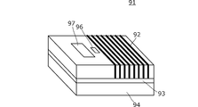
- FIG. 9 is a diagram showing the structure of the RFID tag disclosed in Patent Document 1.
- the RFID tag 91 includes a coil 92, an insulator 93 and a metal plate 94.
- a resonance capacitor 96 and an RFID IC 97 are mounted on the core of the coil.
- the coil opening is relatively small compared to the size of the entire tag. Therefore, the readable distance as an RFID tag is limited.
- the above-mentioned problem is not limited to the RFID tag but is common to a coil module including a coil and a module circuit connected to the coil.
- An object of the present invention is to provide a coil module having a large effective coil opening for the entire size.
- the coil module of the present invention includes: A circuit board on which a conductor pattern is formed; Electronic components mounted on the circuit board and constituting a module circuit with the conductor pattern; A resin layer that seals the electronic component on the circuit board and forms a laminate together with the circuit board; A conductor coil wound around the laminate and connected to the module circuit; It is characterized by providing.
- the conductor coil is wound around the entire laminate of the circuit board and the resin layer that seals the electronic components mounted on the circuit board. Therefore, an effective coil for the entire size.
- a coil module having a coil with a large opening is obtained.
- the resin layer has a top surface parallel to the circuit board and a side surface perpendicular to the circuit board, and the conductor coil is in contact with the top surface and the side surface of the resin layer. It is preferable. Thereby, the external shape of the laminated body by a circuit board and a resin layer is simplified, and winding of a conductor coil becomes easy.
- the top surface of the resin layer has substantially the same shape as the surface of the circuit board on which the electronic component is mounted. Therefore, the external shape of the laminated body by a circuit board and a resin layer is simplified, and winding of a conductor coil becomes easy.
- the electronic component is mounted on the first surface of the circuit board, and the conductor pattern is a terminal electrode formed on the second surface of the circuit board. Preferably, both ends of the conductor coil are connected to the terminal electrode. This structure facilitates connection and winding of the conductor coil to the module circuit.
- the coil module of the present invention includes: An electronic component having a terminal; A resin layer for sealing the electronic component with the terminal of the electronic component exposed; A conductor coil wound around the resin layer and connected to the terminal of the electronic component; It is characterized by providing.
- the coil module having a coil having a large effective coil opening for the entire size. Is obtained.
- the electronic component has a rectangular parallelepiped shape having a first main surface and a second main surface facing the first main surface, and the resin layer is the first main surface of the electronic component.
- the conductor coil is in contact with the top surface, the bottom surface, and the two side surfaces of the resin layer.
- the conductor coil is preferably a Cu wire having an insulating film.
- the conductor coil can be wound in close proximity, or can be wound in an overlapping manner, whereby the self-inductance inductance can be increased and a predetermined inductance can be obtained with a small number of turns.
- a coil antenna is configured by the conductor coil, and the electronic component includes an RFID IC connected to the coil antenna.
- the electronic component includes an RFID IC connected to the coil antenna.
- the conductor coil is wound around the entire laminate including the circuit board and the resin layer that seals the electronic component mounted on the circuit board. Therefore, it is effective for the entire size.
- a coil module having a coil with a large coil opening can be obtained.
- FIG. 1 is a four-side view of an RFID tag 101 as an example of a coil module according to the first embodiment.
- FIG. 2 is a two-side view of a circuit board provided in the RFID tag 101.
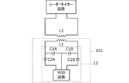
- FIG. 3 is a diagram showing a circuit of the RFID tag 101 and a circuit of the communication partner antenna.
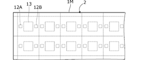
- FIG. 4 is a partial plan view of a state in which a conductor pattern is formed in each circuit formation region of the collective substrate 1M, the electronic component 13 is mounted, and the entire collective substrate 1M is covered with the resin layer 2.
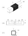
- FIG. 5A is a perspective view of an RFID tag 102 as an example of a coil module according to the second embodiment.
- FIG. 5B is a plan view of the circuit board 1 included in the RFID tag 102.
- FIG. 5C is a side view of the RFID tag 102.
- FIG. 6 is a four-side view of an RFID tag 103 as an example of a coil module according to the third embodiment.
- 7A, 7 ⁇ / b> B, and 7 ⁇ / b> C are diagrams illustrating a state during the manufacturing of the RFID tag 103.
- FIG. 8 is a three-side view of an RFID tag 104 as an example of a coil module according to the fourth embodiment.
- FIG. 9 is a diagram showing the structure of the RFID tag disclosed in Patent Document 1. In FIG.
- the “coil module” shown in the following embodiments is used for near-field communication such as NFC (Near Field Communication) using magnetic field coupling with the communication partner antenna device.
- NFC Near Field Communication
- FIG. 1 is a four-side view of an RFID tag 101 as an example of a coil module according to the first embodiment.
- FIG. 2 is a two-side view of a circuit board provided in the RFID tag 101.
- the RFID tag 101 includes a circuit board 1 and a resin layer 2.
- the circuit board 1 includes a base material 10, wiring conductors 11A and 11B and terminal electrodes 12A and 12B formed on the base material 10.
- the wiring conductors 11A and 11B are electrically connected to the terminal electrodes 12A and 12B through through holes, respectively.
- An electronic component 13 is connected (mounted) to the wiring conductors 11A and 11B.
- the electronic component 13 is an RFID IC.
- the circuit board 1 is, for example, a glass / epoxy board.
- the joining of the electronic component 13 to the wiring conductors 11A and 11B of the circuit board 1 is, for example, solder joining or Au—Au joining.
- a module circuit is configured by the conductor patterns such as the wiring conductors 11A and 11B, the terminal electrodes 12A and 12B, and the electronic component 13. As described above, the electronic component 13 is mounted on the first surface S1 of the circuit board 1, and the terminal electrodes 12A and 12B are formed on the second surface S2 of the circuit board 1.
- the electronic component 13 mounted on the circuit board 1 is sealed with a resin layer 2 made of a thermosetting resin such as an epoxy resin.
- a laminate 123 is constituted by the circuit board 1 and the resin layer 2.
- the conductor coil 4 is wound around the multilayer body 123 in a direction in which the multilayer body 123 is bundled.
- the resin layer 2 has a top surface TS parallel to the circuit board 1 and a side surface SS perpendicular to the circuit board 1, and the conductor coil 4 is in contact with the top surface TS and the side surface SS of the resin layer 2.
- the conductor coil 4 is a Cu wire having a polyurethane film (Cu wire coated with polyurethane).
- the conductor coil 4 is wound about 8 turns in this example.
- the conductor coil 4 acts as a coil antenna.
- Both ends of the conductor coil 4 are connected to the terminal electrodes 12A and 12B.
- the terminal electrodes 12A and 12B are Cu electrode patterns, for example, and are Cu—Cu welded with Cu which is a core material of the conductor coil. Thereby, the conductor coil 4 is connected to the module circuit.
- the magnetic flux ⁇ schematically represents the magnetic flux passing through the coil antenna by the conductor coil 4.
- the coil opening of the conductor coil 4 there are electronic components and conductor patterns in the coil opening of the conductor coil 4, which partially shield the magnetic flux, but the coil opening has a height H, as shown in FIG.
- the width W is larger than the cross section of the circuit board 1 or the resin layer 2 alone.
- the conductor coil 4 can be wound in close proximity or wound in an overlapping manner, whereby the self-inductance inductance can be increased and a predetermined inductance can be obtained with a small number of turns.
- the number of turns or the conductor interval of the conductor coil 4 can be easily adjusted and set without changing the circuit board 1, so that an RFID tag 101 having a coil antenna having a predetermined inductance can be obtained. It is done.
- a magnetic core made of ferrite or the like since a magnetic core made of ferrite or the like is not provided, a magnetic loss does not occur, and a low loss characteristic can be obtained even in a high frequency band above the UHF band, for example.
- FIG. 3 is a diagram showing a circuit of the RFID tag 101 and a circuit of the communication partner antenna.
- the inductor L ⁇ b> 1 corresponds to the conductor coil 4.
- the RFID circuit and the capacitors C1A, C1B, C2A, and C2B are circuits configured in the electronic component 13 mounted on the circuit board 1.
- the capacitors C1A, C1B, C2A, C2B and the inductor L1 constitute an LC resonance circuit and an impedance matching circuit with the RFID-IC.
- the resonance frequency band of this LC resonance circuit is a frequency band used for communication. For example, in the case of NFC, it is 13.56 MHz or a frequency in the vicinity thereof.
- the inductor L2 is an element that represents the coil antenna on the communication partner side as a lumped constant circuit.
- a reader / writer circuit is connected to the inductor L2.
- the inductor L1 by the conductor coil 4 of the RFID tag 101 and the inductor L2 of the communication partner antenna are magnetically coupled.
- FIG. 4 is a partial plan view of a state in which a conductor pattern is formed in each circuit formation region of the collective substrate 1M, the electronic component 13 is mounted, and the entire collective substrate 1M is covered with the resin layer 2.
- the collective board 1M is in a state before being separated into the circuit boards 1 (pieces) shown in FIG.
- the RFID tag 101 is manufactured by the following procedure.
- the resin layer 2 is formed by applying a sealing resin such as an epoxy resin on the electronic component mounting surface of the collective substrate 1M. Moreover, an underfill is formed between the collective substrate 1M and the electronic component 13 (gap on the lower surface of the electronic component) by vacuum degassing.
- a sealing resin such as an epoxy resin
- the collective substrate 1M is cut with a dicer and divided into individual pieces. Thereby, the some laminated body 123 is obtained.
- a broken line extending vertically and horizontally is a cutting line by a dicer.
- the conductor coil 4 is formed by winding the insulation coating Cu wire around each laminated body 123 using a coil winding machine.
- a coil winding machine a winding machine for manufacturing a chip-shaped winding inductor can be used.
- the RFID tag 101 shown in FIG. 1 is dipped in a liquid resin, pulled up, and cured by heating to apply a resin coating around the RFID tag 101.
- the RFID tag 101 is manufactured by the above procedure.
- the completed RFID tag 101 is attached to an article such as a toy, for example.
- the article is a resin molded product
- the RFID tag 101 is integrated with the article so that the RFID tag 101 is embedded in the resin during injection molding of the resin.
- Second Embodiment An example in which the configuration of the resin layer is different from that of the first embodiment is shown.
- FIG. 5A is a perspective view of an RFID tag 102 as an example of a coil module according to the second embodiment.
- FIG. 5B is a plan view of the circuit board 1 included in the RFID tag 102.
- FIG. 5C is a side view of the RFID tag 102.
- the RFID tag 102 includes a circuit board 1 and a resin layer 2.
- the basic configuration of the circuit board 1 and the conductor coil 4 is the same as that of the RFID tag 101 shown in the first embodiment.
- the laminate of the circuit board 1 and the resin layer 2 is a regular quadrangular prism.
- the longitudinal dimension of this laminated body is three times or more the height dimension or the width dimension, and it can also be said to be a form like a shaft of a match rod. Therefore, a region where the conductor coil 4 is not wound (non-winding region) is long in the coil axis direction.
- the external size of the RFID tag 102 is, for example, 4 mm ⁇ 1 mm ⁇ 1 mm.
- the coil winding machine can easily chuck the laminate. Further, since the laminated body is in the shape of a regular quadrangular prism, vibration during winding of the conductor coil 4 is suppressed, and accordingly, high-speed winding is possible.
- FIG. 6 is a four-side view of an RFID tag 103 as an example of a coil module according to the third embodiment.
- 7A, 7 ⁇ / b> B, and 7 ⁇ / b> C are diagrams illustrating a state during the manufacturing of the RFID tag 103.
- the RFID tag 103 includes a resin layer 2 and an electronic component 13 embedded in the resin layer 2.
- a conductor coil 4 is wound around the resin layer 2 around the resin layer 2.
- the terminals 14A, 14B, 14C, and 14D are exposed on the bottom surface of the resin layer 2, and the conductor coil 4 is connected to the terminals 14A and 14B.
- the terminals 14C and 14D are dummy terminals generated in the manufacturing process described later.
- the method for embedding the electronic component 13 in the resin layer 2 is as follows.
- the electronic component 13 is mounted on the substrate 10 via the solder bumps SB.
- the thickness dimension of the resin layer 2 may be made highly accurate by grinding the top surface TS of the resin layer 2.
- Each process described above is processed in a collective substrate state, and is cut into pieces as shown in FIG. 7C by cutting with a dicer in the final process.
- FIG. 8 is a three-side view of an RFID tag 104 as an example of a coil module according to the fourth embodiment.
- the RFID tag 104 includes a circuit board 1 and a resin layer 2.
- the circuit board 1 has a conductor pattern formed only on its upper surface.
- the electronic component 13 and the columnar conductors 15A and 15B are mounted on the upper surface of the circuit board 1.
- the electronic component 13 and the columnar conductors 15A and 15B are connected via the wiring conductors 11A and 11B.
- the columnar conductors 15A and 15B are exposed on the upper surface of the resin layer 2.
- the conductor coil 4 is connected to the exposed portions of the columnar conductors 15A and 15B.
- columnar conductors 15A and 15B for example, conductor pins can be used.
- a hole is formed in the resin layer 2 by laser processing, a method of plating a conductor film on the inner surface, or a method of injecting a conductive member into the hole, and using this hole as a columnar conductor You may make it act.
- the conductor coil may be polyester, polyimide, polyamide, or the like. It may be a coil of a conductor wire covered with.
- the magnetic loss is small, and therefore a part or all of the base material of the circuit board 1 may be a magnetic material. If it is a magnetic body, since the circuit board 1 acts as a magnetic body core, an effective coil opening becomes large.
- the RFID tag is taken as an example in the embodiment described above, it can be similarly applied to a coil module having a coil having a large effective coil opening.
- the present invention can be applied to a communication module including a coil antenna and a high-frequency circuit connected to the coil antenna.
Landscapes
- Engineering & Computer Science (AREA)
- Power Engineering (AREA)
- Microelectronics & Electronic Packaging (AREA)
- Computer Hardware Design (AREA)
- Physics & Mathematics (AREA)
- General Physics & Mathematics (AREA)
- Theoretical Computer Science (AREA)
- Coils Or Transformers For Communication (AREA)
- Credit Cards Or The Like (AREA)
Abstract
コイルモジュールであるRFIDタグ(101)は、導体パターンが形成された回路基板(1)と、この回路基板(1)に実装され、導体パターンとでモジュール用回路を構成する電子部品(13)と、電子部品(13)を回路基板(1)上で封止し、回路基板(1)とともに積層体を形成する樹脂層(2)と、積層体(123)の周囲に巻回され、モジュール用回路に接続された導体コイル(4)と、を備える。この構成により、コイル開口を通過する磁束が遮蔽され難く、全体のサイズの割には実効的なコイル開口が大きいコイルモジュールを得る。
Description
本発明は、コイルと、そのコイルに接続された回路とを備えるコイルモジュールに関する。
金属ワイヤーによるコイルを備えるRFIDタグが、例えば特許文献1に示されている。図9は特許文献1に示されているRFIDタグの構造を示す図である。図9において、RFIDタグ91は、コイル92、絶縁物93および金属板94を備える。また、コイルのコアに共振用のコンデンサ96およびRFID用IC97が搭載されている。
上記金属ワイヤーが巻回されたRFIDタグにおいては、コイルはコア(磁芯)に巻回されているだけであるので、タグ全体のサイズに比べてコイル開口は比較的小さい。したがって、RFIDタグとしての読み取り可能距離が制限を受ける構造であった。
上述の課題はRFIDタグに限らず、コイルとそれに接続されたモジュール用回路とを備えるコイルモジュールに共通の課題である。
本発明の目的は、全体のサイズの割には実効的なコイル開口が大きい、コイルモジュールを提供することにある。
(1)本発明のコイルモジュールは、
導体パターンが形成された回路基板と、
前記回路基板に実装され、前記導体パターンとでモジュール用回路を構成する電子部品と、
前記電子部品を前記回路基板上で封止し、前記回路基板とともに積層体を形成する樹脂層と、
前記積層体の周囲に巻回され、前記モジュール用回路に接続された導体コイルと、
を備えることを特徴とする。
導体パターンが形成された回路基板と、
前記回路基板に実装され、前記導体パターンとでモジュール用回路を構成する電子部品と、
前記電子部品を前記回路基板上で封止し、前記回路基板とともに積層体を形成する樹脂層と、
前記積層体の周囲に巻回され、前記モジュール用回路に接続された導体コイルと、
を備えることを特徴とする。
上記構成により、回路基板と、この回路基板に実装された電子部品を封止する樹脂層とによる積層体の全体に導体コイルが巻回されるので、全体のサイズの割には実効的なコイル開口の大きなコイルを有するコイルモジュールが得られる。
(2)上記(1)において、前記樹脂層は前記回路基板に平行な天面および前記回路基板に垂直な側面を有し、前記導体コイルは前記樹脂層の前記天面および前記側面に接する、ことが好ましい。これにより、回路基板および樹脂層による積層体の外形形状は単純化され、導体コイルの巻回が容易となる。
(3)上記(2)において、前記樹脂層の前記天面は、前記電子部品が実装された前記回路基板の面と略同形状であることが好ましい。これにより、回路基板および樹脂層による積層体の外形形状は単純化され、導体コイルの巻回が容易となる。
(4)上記(1)から(3)のいずれかにおいて、前記電子部品は前記回路基板の第1面に実装され、前記導体パターンは、前記回路基板の第2面に形成された端子電極を含み、前記導体コイルの両端は前記端子電極に接続される、ことが好ましい。この構造により、モジュール用回路に対する導体コイルの接続および巻回が容易となる。
(5)本発明のコイルモジュールは、
端子を有する電子部品と、
前記電子部品の前記端子を露出させた状態で前記電子部品を封止する樹脂層と、
前記樹脂層の周囲に巻回され、前記電子部品の前記端子に接続された導体コイルと、
を備えることを特徴とする。
端子を有する電子部品と、
前記電子部品の前記端子を露出させた状態で前記電子部品を封止する樹脂層と、
前記樹脂層の周囲に巻回され、前記電子部品の前記端子に接続された導体コイルと、
を備えることを特徴とする。
上記構成により、回路基板を含まずに、電子部品を封止する樹脂層の周囲に導体コイルが巻回されるので、全体のサイズの割には実効的なコイル開口の大きなコイルを有するコイルモジュールが得られる。
(6)上記(5)において、前記電子部品は第1主面および当該第1主面に対向する第2主面を有する直方体状であり、前記樹脂層は前記電子部品の前記第1主面に平行な天面および底面、前記天面および前記底面を接続する二つの側面を有し、前記導体コイルは前記樹脂層の前記天面、前記底面および前記二つの側面に接することが好ましい。これにより、回路基板および樹脂層による積層体の外形形状は単純化され、導体コイルの巻回が容易となる。
(7)上記(1)から(6)のいずれかにおいて、前記導体コイルは絶縁皮膜を有するCu線であることが好ましい。これにより、導体コイルを極近接して巻回、または重ねて巻回することができ、そのことで、自己誘導インダクタンスを大きくでき、少ないターン数で所定のインダクタンスを得ることができる。
(8)上記(1)から(7)のいずれかにおいて、例えば、前記導体コイルでコイルアンテナが構成され、前記電子部品は前記コイルアンテナに接続されるRFID用ICを含む。これにより、小型でありながら通信可能距離の大きなRFIDタグが構成される。
本発明によれば、回路基板と、この回路基板に実装された電子部品を封止する樹脂層とによる積層体の全体に導体コイルが巻回されるので、全体のサイズの割には実効的なコイル開口の大きなコイルを有するコイルモジュールが得られる。
以降、図を参照して幾つかの具体的な例を挙げて、本発明を実施するための複数の形態を示す。各図中には同一箇所に同一符号を付している。要点の説明または理解の容易性を考慮して、便宜上実施形態を分けて示すが、異なる実施形態で示した構成の部分的な置換または組み合わせは可能である。第2の実施形態以降では第1の実施形態と共通の事柄についての記述を省略し、異なる点についてのみ説明する。特に、同様の構成による同様の作用効果については実施形態毎には逐次言及しない。
以降に示す各実施形態に示す「コイルモジュール」は、通信相手側アンテナ装置と磁界結合を用いた、例えばNFC(Near field communication)等の近傍界通信のために用いられる。
《第1の実施形態》
図1は第1の実施形態に係るコイルモジュールの一例としてのRFIDタグ101の四面図である。図2はRFIDタグ101が備える回路基板の二面図である。
図1は第1の実施形態に係るコイルモジュールの一例としてのRFIDタグ101の四面図である。図2はRFIDタグ101が備える回路基板の二面図である。
図1に表れているように、RFIDタグ101は、回路基板1および樹脂層2を備える。
図2に表れているように、回路基板1は、基材10と、この基材10に形成された配線導体11A,11Bおよび端子電極12A,12Bを備える。配線導体11A,11Bは端子電極12A,12Bにそれぞれスルーホールを介して電気的に導通している。配線導体11A,11Bには電子部品13が接続(実装)されている。電子部品13はRFID用ICである。回路基板1は例えばガラス・エポキシ基板である。回路基板1の配線導体11A,11Bへの電子部品13の接合は、例えばはんだ接合やAu-Au接合である。上記配線導体11A,11B、端子電極12A,12B等の導体パターンおよび電子部品13によってモジュール用回路が構成されている。このように、回路基板1の第1面S1に電子部品13が実装されていて、回路基板1の第2面S2に端子電極12A,12Bが形成されている。
図1に表れているように、回路基板1に実装されている電子部品13は、例えばエポキシ樹脂等の熱硬化性樹脂による樹脂層2で封止されている。回路基板1および樹脂層2によって積層体123が構成されている。この積層体123の周囲に、積層体123を束ねる方向に導体コイル4が巻回されている。
樹脂層2は回路基板1に平行な天面TSおよび回路基板1に垂直な側面SSを有し、導体コイル4は樹脂層2の天面TSおよび側面SSに接する。
導体コイル4はポリウレタン皮膜を有するCu線(ポリウレタンが被覆されたCu線)である。導体コイル4は、この例では約8ターン巻回されている。導体コイル4はコイルアンテナとして作用する。
上記導体コイル4の両端は端子電極12A,12Bに接続されている。端子電極12A,12Bは例えばCu電極パターンであり、導体コイルの芯材であるCuとで、Cu-Cu溶接される。これにより、導体コイル4は上記モジュール用回路に接続される。
図1において磁束φは導体コイル4によるコイルアンテナを通過する磁束を概略的に表している。
本実施形態によれば、導体コイル4のコイル開口内に電子部品や導体パターンが存在し、これらが磁束を部分的に遮蔽するが、コイル開口は、図1に示すように、高さH、幅Wであり、回路基板1単体や樹脂層2単体の断面より大きい。例えばH=2.3mm、W=5mmである。このように、外形サイズの割に大きなコイル開口のコイルを備えるため、結合相手のコイルとの結合係数の高いRFIDタグが得られる。
また、導体コイル4を極近接して巻回、または重ねて巻回することができ、そのことで、自己誘導インダクタンスを大きくでき、少ないターン数で所定のインダクタンスを得ることができる。
また、本実施形態によれば、回路基板1を変更することなく、導体コイル4の巻回数または導体間隔を容易に調整・設定できるので、所定のインダクタンスを有するコイルアンテナを有するRFIDタグ101が得られる。
また、本実施形態によれば、フェライト等による磁芯を備えないので磁気損失が生じることなく、例えばUHF帯以上の高周波帯でも低損失特性が得られる。
図3はRFIDタグ101の回路および通信相手側アンテナの回路を示す図である。図3において、インダクタL1は導体コイル4に対応する。RFID回路、キャパシタC1A,C1B,C2A,C2Bは回路基板1に実装されている電子部品13に構成されている回路である。
キャパシタC1A,C1B,C2A,C2BおよびインダクタL1は、LC共振回路を構成するとともに、RFID-ICとのインピーダンス整合回路を構成している。このLC共振回路の共振周波数帯は、通信に利用される周波数帯である。例えばNFCの場合、13.56MHzまたはその近傍の周波数である。
インダクタL2は通信相手側のコイルアンテナを集中定数回路として表した素子である。インダクタL2にはリーダ・ライター回路が接続されている。RFIDタグ101の導体コイル4によるインダクタL1と通信相手側アンテナのインダクタL2とは磁界結合する。
次に、本実施形態のRFIDタグ101の製造方法の一例を示す。図4は集合基板1Mの各回路形成領域にそれぞれ導体パターンが形成され、電子部品13が実装され、集合基板1Mの全体が樹脂層2で被覆された状態での部分平面図である。集合基板1Mは図2に示した回路基板1(個片)への分離前の状態である。
RFIDタグ101は次の手順で製造する。
(1)先ず、図4に示す集合基板1Mの各回路形成領域に導体パターンを形成し、各回路形成領域に電子部品13を実装する。
(2)集合基板1Mの電子部品実装面に、例えばエポキシ樹脂等の封止樹脂を塗布することで樹脂層2を形成する。また、真空脱泡することで、集合基板1Mと電子部品13との間(電子部品の下面の間隙)にアンダーフィルを形成する。
(3)上記樹脂層2を加熱硬化させる。
(4)集合基板1Mを、ダイサーで切削し、個片に分割する。これにより、複数の積層体123を得る。図4において縦横に延びる破線はダイサーによる切削線である。
(5)コイル巻回マシンを用いて、各積層体123に絶縁被覆Cu線を巻回することによって、導体コイル4を形成する。このコイル巻回マシンには、チップ状の巻線インダクタを製造する巻回マシンを利用できる。
(6)その後、必要に応じて、図1に示したRFIDタグ101を液状樹脂に浸漬し、引き上げ、加熱硬化させることによって、RFIDタグ101の周囲に樹脂コーティングを施す。
以上の手順によってRFIDタグ101を製造する。なお、完成したRFIDタグ101は、例えば玩具等の物品に装着する。物品が樹脂成形品である場合には、樹脂の射出成型時に、その樹脂中にRFIDタグ101が埋設されるようにRFIDタグ101を物品に一体化させる。
《第2の実施形態》
第2の実施形態では、樹脂層の構成が第1の実施形態とは異なる例を示す。
第2の実施形態では、樹脂層の構成が第1の実施形態とは異なる例を示す。
図5(A)は第2の実施形態に係るコイルモジュールの一例としてのRFIDタグ102の斜視図である。図5(B)は、RFIDタグ102が備える回路基板1の平面図である。図5(C)はRFIDタグ102の側面図である。
図5(A)(C)に表れているように、RFIDタグ102は、回路基板1および樹脂層2を備える。回路基板1、導体コイル4の基本構成は第1の実施形態で示したRFIDタグ101と同様であるが、本実施形態では、回路基板1と樹脂層2とによる積層体は正四角柱状である。また、この積層体の長手方向寸法は、高さ寸法または幅寸法の3倍以上であり、マッチ棒の軸のような形態ということもできる。そのため、導体コイル4を巻回しない領域(非巻回領域)がコイル軸方向に長い。RFIDタグ102の外形サイズは例えば4mm×1mm×1mmである。
本実施形態によれば、上記非巻回領域がコイル軸方向に長いので、コイル巻回マシンが積層体をチャッキングし易い。また、積層体は正四角柱状であるので、導体コイル4の巻回時の振動が抑えられ、その分、高速巻回が可能となる。
なお、コイルマシンによる導体コイルの巻回工程の後、上記積層体の両端部の、電磁気的に不要な部分を切断して短縮化してもよい。
《第3の実施形態》
第3の実施形態では、回路基板を備えないRFIDタグの例を示す。
第3の実施形態では、回路基板を備えないRFIDタグの例を示す。
図6は第3の実施形態に係るコイルモジュールの一例としてのRFIDタグ103の四面図である。図7(A)(B)(C)はRFIDタグ103の製造途中の状態を示す図である。
図6に表れているように、RFIDタグ103は、樹脂層2と、この樹脂層2の内部に埋設された電子部品13を備える。樹脂層2の周囲には、樹脂層2の周囲に導体コイル4が巻回されている。樹脂層2の底面には端子14A,14B,14C,14Dが露出していて、導体コイル4は端子14A,14Bに接続されている。端子14C,14Dは、後述する製造工程上生じるダミー端子である。
樹脂層2内に電子部品13を埋設する方法は次のとおりである。
(1)先ず、図7(A)に示すように、基材10にはんだバンプSBを介して電子部品13を実装する。
(2)次に、基材10の電子部品実装面にエポキシ樹脂等を塗布し、硬化させることで、樹脂被覆体を構成する。
(3)その後、上記樹脂被覆体を、図7(B)に示す研削面GSまで研削することで、図7(C)に示す状態とする。これにより、はんだバンプSBが露出し、この露出部が前述の端子14A~14Dとして用いられる。
なお、樹脂層2の天面TSを研削することで、樹脂層2の厚み寸法を高精度化してもよい。
上述の各工程は集合基板状態で処理され、最終工程でダイサーで切削されることにより、図7(C)に示した個片に分割される。
《第4の実施形態》
第4の実施形態では、樹脂層の外面に導体コイルの始点と終点を設けたRFIDタグの例を示す。
第4の実施形態では、樹脂層の外面に導体コイルの始点と終点を設けたRFIDタグの例を示す。
図8は第4の実施形態に係るコイルモジュールの一例としてのRFIDタグ104の三面図である。
図8に表れているように、RFIDタグ104は、回路基板1および樹脂層2を備える。回路基板1はその上面にのみ導体パターンが形成されている。回路基板1の上面には電子部品13および柱状導体15A,15Bが実装されている、電子部品13と柱状導体15A,15Bは配線導体11A,11Bを介して接続されている。
柱状導体15A,15Bは樹脂層2の上面に露出している。導体コイル4は柱状導体15A,15Bの露出部にそれぞれ接続されている。
本実施形態によれば、回路基板にスルーホールを形成する必要が無く、製造コストが低減される。
なお、柱状導体15A,15Bとしては、例えば、導体ピンを用いることができる。導体ピンを用いる方法以外に、樹脂層2にレーザー加工によりホールを形成し、その内面に導体膜をめっきする方法や、ホールの内部に導電性部材を注入する方法で、このホールを柱状導体として作用させてもよい。
《その他の実施形態》
以上に示した各実施形態では、ポリウレタン被膜の導体コイルを用いる例を示したが、樹脂の射出成型等、物品への埋設時に加わる温度に応じて、上記導体コイルは例えばポリエステル、ポリイミド、ポリアミド等で被覆された導体線のコイルであってもよい。
以上に示した各実施形態では、ポリウレタン被膜の導体コイルを用いる例を示したが、樹脂の射出成型等、物品への埋設時に加わる温度に応じて、上記導体コイルは例えばポリエステル、ポリイミド、ポリアミド等で被覆された導体線のコイルであってもよい。
コイルモジュールの使用周波数帯がHF帯以下であれば、磁気損失は少ないので、回路基板1の基材の一部または全部は磁性体であってもよい。磁性体であれば、回路基板1が磁性体コアとして作用するので、実効的なコイル開口が大きくなる。
また、以上に示した例では、コイル導体を単層巻きした例を挙げたが、複数層に重ね巻きすることも可能であり、そのことで、小型でありながら所定の高いインダクタンスを有するコイルアンテナが構成できる。
さらに、以上に示した実施形態ではRFIDタグを例に挙げたが、実効的なコイル開口が大きなコイルを有するコイルモジュールに同様に適用できる。例えばコイルアンテナとそのコイルアンテナに接続される高周波回路を備える通信モジュールにも適用できる。
最後に、上述の実施形態の説明は、すべての点で例示であって、制限的なものではない。当業者にとって変形および変更が適宜可能である。本発明の範囲は、上述の実施形態ではなく、特許請求の範囲によって示される。さらに、本発明の範囲には、特許請求の範囲内と均等の範囲内での実施形態からの変更が含まれる。
C1A,C1B,C2A,C2B…キャパシタ
GS…研削面
L1,L2…インダクタ
SB…はんだバンプ
S1…第1面
S2…第2面
SS…側面
TS…天面
1…回路基板
1M…集合基板
2…樹脂層
4…導体コイル
10…基材
11A,11B…配線導体
12A,12B…端子電極
13…電子部品
14A,14B,14C,14D…端子
15A,15B…柱状導体
91…RFIDタグ
92…コイル
93…絶縁物
94…金属板
96…コンデンサ
97…IC
101~104…RFIDタグ(コイルモジュール)
123…積層体
GS…研削面
L1,L2…インダクタ
SB…はんだバンプ
S1…第1面
S2…第2面
SS…側面
TS…天面
1…回路基板
1M…集合基板
2…樹脂層
4…導体コイル
10…基材
11A,11B…配線導体
12A,12B…端子電極
13…電子部品
14A,14B,14C,14D…端子
15A,15B…柱状導体
91…RFIDタグ
92…コイル
93…絶縁物
94…金属板
96…コンデンサ
97…IC
101~104…RFIDタグ(コイルモジュール)
123…積層体
Claims (8)
- 導体パターンが形成された回路基板と、
前記回路基板に実装され、前記導体パターンとでモジュール用回路を構成する電子部品と、
前記電子部品を前記回路基板上で封止し、前記回路基板とともに積層体を形成する樹脂層と、
前記積層体の周囲に巻回され、前記モジュール用回路に接続された導体コイルと、
を備える、コイルモジュール。 - 前記樹脂層は前記回路基板に平行な天面および前記回路基板に垂直な側面を有し、
前記導体コイルは前記樹脂層の前記天面および前記側面に接する、請求項1に記載のコイルモジュール。 - 前記樹脂層の前記天面は、前記電子部品が実装された前記回路基板の面と略同形状である、請求項2に記載のコイルモジュール。
- 前記電子部品は前記回路基板の第1面に実装され、
前記導体パターンは、前記回路基板の第2面に形成された端子電極を含み、
前記導体コイルの両端は前記端子電極に接続される、請求項1から3のいずれかに記載のコイルモジュール。 - 端子を有する電子部品と、
前記電子部品の前記端子を露出させた状態で前記電子部品を封止する樹脂層と、
前記樹脂層の周囲に巻回され、前記電子部品の前記端子に接続された導体コイルと、
を備える、コイルモジュール。 - 前記電子部品は第1主面および当該第1主面に対向する第2主面を有する直方体状であり、
前記樹脂層は前記電子部品の前記第1主面に平行な天面および底面、前記天面および前記底面を接続する二つの側面を有し、
前記導体コイルは前記樹脂層の前記天面、前記底面および前記二つの側面に接する、請求項5に記載のコイルモジュール。 - 前記導体コイルは絶縁皮膜を有するCu線である、請求項1から6のいずれかに記載のコイルモジュール。
- 前記導体コイルでコイルアンテナが構成され、前記電子部品は前記コイルアンテナに接続されるRFID用ICを含む、請求項1から7のいずれかに記載のコイルモジュール。
Priority Applications (1)
| Application Number | Priority Date | Filing Date | Title |
|---|---|---|---|
| JP2018524982A JP6648830B2 (ja) | 2016-07-01 | 2017-06-02 | コイルモジュール |
Applications Claiming Priority (2)
| Application Number | Priority Date | Filing Date | Title |
|---|---|---|---|
| JP2016131899 | 2016-07-01 | ||
| JP2016-131899 | 2016-07-01 |
Publications (1)
| Publication Number | Publication Date |
|---|---|
| WO2018003398A1 true WO2018003398A1 (ja) | 2018-01-04 |
Family
ID=60786040
Family Applications (1)
| Application Number | Title | Priority Date | Filing Date |
|---|---|---|---|
| PCT/JP2017/020537 Ceased WO2018003398A1 (ja) | 2016-07-01 | 2017-06-02 | コイルモジュール |
Country Status (2)
| Country | Link |
|---|---|
| JP (1) | JP6648830B2 (ja) |
| WO (1) | WO2018003398A1 (ja) |
Cited By (4)
| Publication number | Priority date | Publication date | Assignee | Title |
|---|---|---|---|---|
| JP6562193B1 (ja) * | 2018-01-23 | 2019-08-21 | 株式会社村田製作所 | Rfidタグ、rfidタグを備えた物品、および物品の製造方法 |
| JP6590128B1 (ja) * | 2018-04-17 | 2019-10-16 | 株式会社村田製作所 | Rfidタグ |
| WO2019202817A1 (ja) * | 2018-04-17 | 2019-10-24 | 株式会社村田製作所 | Rfidタグ |
| JPWO2024106370A1 (ja) * | 2022-11-14 | 2024-05-23 |
Citations (2)
| Publication number | Priority date | Publication date | Assignee | Title |
|---|---|---|---|---|
| JP2001510914A (ja) * | 1997-07-14 | 2001-08-07 | アーエーゲー イデンティフィカツィオーンスジステーメ ゲゼルシャフト ミット ベシュレンクテル ハフツング | トランスポンダ装置およびその製造方法 |
| WO2009145218A1 (ja) * | 2008-05-28 | 2009-12-03 | 株式会社村田製作所 | 無線icデバイス用部品および無線icデバイス |
-
2017
- 2017-06-02 JP JP2018524982A patent/JP6648830B2/ja active Active
- 2017-06-02 WO PCT/JP2017/020537 patent/WO2018003398A1/ja not_active Ceased
Patent Citations (2)
| Publication number | Priority date | Publication date | Assignee | Title |
|---|---|---|---|---|
| JP2001510914A (ja) * | 1997-07-14 | 2001-08-07 | アーエーゲー イデンティフィカツィオーンスジステーメ ゲゼルシャフト ミット ベシュレンクテル ハフツング | トランスポンダ装置およびその製造方法 |
| WO2009145218A1 (ja) * | 2008-05-28 | 2009-12-03 | 株式会社村田製作所 | 無線icデバイス用部品および無線icデバイス |
Cited By (5)
| Publication number | Priority date | Publication date | Assignee | Title |
|---|---|---|---|---|
| JP6562193B1 (ja) * | 2018-01-23 | 2019-08-21 | 株式会社村田製作所 | Rfidタグ、rfidタグを備えた物品、および物品の製造方法 |
| JP6590128B1 (ja) * | 2018-04-17 | 2019-10-16 | 株式会社村田製作所 | Rfidタグ |
| WO2019202817A1 (ja) * | 2018-04-17 | 2019-10-24 | 株式会社村田製作所 | Rfidタグ |
| JPWO2024106370A1 (ja) * | 2022-11-14 | 2024-05-23 | ||
| JP7733359B2 (ja) | 2022-11-14 | 2025-09-03 | 株式会社村田製作所 | Rfidモジュール |
Also Published As
| Publication number | Publication date |
|---|---|
| JP6648830B2 (ja) | 2020-02-14 |
| JPWO2018003398A1 (ja) | 2019-05-16 |
Similar Documents
| Publication | Publication Date | Title |
|---|---|---|
| US9691539B2 (en) | Coil component | |
| US10784929B2 (en) | Wireless IC device | |
| US8602310B2 (en) | Radio communication device and radio communication terminal | |
| JP5573937B2 (ja) | アンテナモジュール | |
| US10411325B2 (en) | Antenna device, antenna module, and communication terminal apparatus | |
| JP6648830B2 (ja) | コイルモジュール | |
| US10122068B2 (en) | Wireless IC device, molded resin article, and method for manufacturing coil antenna | |
| WO2016143425A1 (ja) | 無線icデバイス、それを備えた樹脂成型体、それを備えた通信端末装置、及びその製造方法 | |
| CN207529410U (zh) | Rfic设备 | |
| JP6187728B1 (ja) | 無線通信デバイス、及びその製造方法 | |
| WO2017159436A1 (ja) | コイルモジュール | |
| WO2018012378A1 (ja) | コイルモジュール | |
| JP6789202B2 (ja) | ブースターアンテナ | |
| JP7733359B2 (ja) | Rfidモジュール | |
| JP2017135481A (ja) | コイルデバイスおよび無線icデバイス | |
| WO2017141771A1 (ja) | 無線通信デバイス及びその製造方法、並びに、樹脂成型体 | |
| US11699057B2 (en) | RFID tag and method for producing the same | |
| JP6160796B1 (ja) | 無線通信デバイス及びその製造方法、並びに、樹脂成型体 | |
| KR102342732B1 (ko) | 주기적인 금속 패턴 구조를 이용하여 q 인자가 향상된 인덕터 소자 | |
| JP6376308B2 (ja) | 無線icデバイスおよび無線icデバイスの製造方法 | |
| JP3055075B2 (ja) | インダクタ及びその製造方法 | |
| JP2025124336A (ja) | コイル装置 | |
| HK1259475B (zh) | Rfid标签 |
Legal Events
| Date | Code | Title | Description |
|---|---|---|---|
| 121 | Ep: the epo has been informed by wipo that ep was designated in this application |
Ref document number: 17819763 Country of ref document: EP Kind code of ref document: A1 |
|
| ENP | Entry into the national phase |
Ref document number: 2018524982 Country of ref document: JP Kind code of ref document: A |
|
| NENP | Non-entry into the national phase |
Ref country code: DE |
|
| 122 | Ep: pct application non-entry in european phase |
Ref document number: 17819763 Country of ref document: EP Kind code of ref document: A1 |