WO2018003239A2 - アンテナ装置および電子機器 - Google Patents
アンテナ装置および電子機器 Download PDFInfo
- Publication number
- WO2018003239A2 WO2018003239A2 PCT/JP2017/015270 JP2017015270W WO2018003239A2 WO 2018003239 A2 WO2018003239 A2 WO 2018003239A2 JP 2017015270 W JP2017015270 W JP 2017015270W WO 2018003239 A2 WO2018003239 A2 WO 2018003239A2
- Authority
- WO
- WIPO (PCT)
- Prior art keywords
- coil
- antenna device
- antenna
- planar conductor
- circuit board
- Prior art date
- Legal status (The legal status is an assumption and is not a legal conclusion. Google has not performed a legal analysis and makes no representation as to the accuracy of the status listed.)
- Ceased
Links
Images





Classifications
-
- H—ELECTRICITY
- H01—ELECTRIC ELEMENTS
- H01Q—ANTENNAS, i.e. RADIO AERIALS
- H01Q1/00—Details of, or arrangements associated with, antennas
- H01Q1/12—Supports; Mounting means
- H01Q1/22—Supports; Mounting means by structural association with other equipment or articles
- H01Q1/24—Supports; Mounting means by structural association with other equipment or articles with receiving set
-
- H—ELECTRICITY
- H01—ELECTRIC ELEMENTS
- H01Q—ANTENNAS, i.e. RADIO AERIALS
- H01Q1/00—Details of, or arrangements associated with, antennas
- H01Q1/52—Means for reducing coupling between antennas; Means for reducing coupling between an antenna and another structure
-
- H—ELECTRICITY
- H01—ELECTRIC ELEMENTS
- H01Q—ANTENNAS, i.e. RADIO AERIALS
- H01Q7/00—Loop antennas with a substantially uniform current distribution around the loop and having a directional radiation pattern in a plane perpendicular to the plane of the loop
- H01Q7/06—Loop antennas with a substantially uniform current distribution around the loop and having a directional radiation pattern in a plane perpendicular to the plane of the loop with core of ferromagnetic material
-
- H—ELECTRICITY
- H04—ELECTRIC COMMUNICATION TECHNIQUE
- H04M—TELEPHONIC COMMUNICATION
- H04M1/00—Substation equipment, e.g. for use by subscribers
- H04M1/02—Constructional features of telephone sets
Definitions
- the present invention relates to an antenna device that is housed in a casing of an electronic device or partially includes the casing of the electronic device.
- a planar conductor having an opening, such as a metal part of a housing, and a coil antenna are provided, and the coil antenna and the planar conductor are coupled by overlapping the coil opening on the planar conductor, and the planar conductor is used as a booster.
- a used antenna apparatus is disclosed in Patent Document 1.
- Patent Document 1 discloses that a camera module is arranged at the position of the opening.
- the planar conductor coupled to the coil antenna may be a ground conductor formed on the circuit board, a shield case fixed to the circuit board, or the like.
- the cable drawn from the camera module is connected to the circuit board, the cable is located between the coil antenna and the planar conductor in the normal direction of the main surface of the planar conductor, so that the cable is It is susceptible to magnetic flux interference generated from planar conductors and coil conductors.
- the inventor of the present invention has found that the interference received by the cable of the camera module may hinder the operation of the camera module, for example, a noise component is superimposed on the image signal.
- Such an operational obstacle is a problem to be solved not only in the camera module but also in an antenna device including a coil antenna and a planar conductor and configured with functional parts.
- An object of the present invention is to provide an antenna device that includes a coil antenna and a planar conductor, and that is configured with a functional component, and that solves the problem of interference received by the cable of the functional component, and an electronic apparatus including the antenna device. There is.
- the antenna device of the present invention A circuit board; A planar conductor provided on the circuit board and formed with a notch having an outer edge; A functional component having a main body and a cable drawn from the main body and connected to the circuit board, the main body overlapping the notch in a plan view of the planar conductor; A coil antenna composed of a coil conductor wound around the body of the functional component; With The cable is located between the coil antenna and the planar conductor; The drawing direction of the cable from the body of the functional component is a direction that does not intersect the outer edge in a plan view of the planar conductor.
- the planar conductor is a ground conductor formed on the circuit board. Accordingly, it is not necessary to form a planar conductor dedicated to the antenna device, and an antenna device having a large effective antenna area can be provided while being a small electronic device.
- a magnetic material is further provided at least in a portion where the coil conductor and the cable overlap with each other when arranged between the coil antenna and the planar conductor in a plan view of the planar conductor. Thereby, unnecessary magnetic field coupling between the coil conductor and the cable of the functional component is suppressed.
- the said coil conductor has a part which opposes the said planar conductor not through the said magnetic body. Therefore, the required coupling
- Conductivity having a smaller area than that of the planar conductor is disposed between the coil antenna and the planar conductor, and at least a portion where the coil conductor and the cable overlap in a plan view of the planar conductor. It is preferable to provide a sex member. Thereby, unnecessary electromagnetic coupling between the coil conductor and the cable of the functional component is suppressed.
- a conductive material having a smaller area than that of the planar conductor is disposed between the coil antenna and the planar conductor, and at least a portion where the coil conductor and the cable overlap in a plan view of the planar conductor. It is preferable that a conductive member and a magnetic body are provided, and the conductive member is disposed between the magnetic body and the planar conductor. This suppresses the electromagnetic coupling between the coil conductor and the cable via the magnetic flux interlinking with the coil conductor while suppressing the decrease in the magnetic flux interlinking with the coil conductor due to the conductive member.
- the functional component may be an optical component such as a camera module, a flash, an infrared sensor, or a display.
- the functional component may be an operation component such as a pressing switch.
- An electronic device of the present invention includes an antenna device housed in a housing,
- the antenna device is A circuit board;
- a functional component having a main body and a cable drawn from the main body and connected to the circuit board, the main body overlapping the notch in a plan view of the planar conductor;
- a coil antenna composed of a coil conductor wound around the body of the functional component; With The cable is located between the coil antenna and the planar conductor;
- the drawing direction of the cable from the body of the functional component is a direction that does not intersect the outer edge in a plan view of the planar conductor.
- the cable of the functional component is not easily affected by magnetic flux generated from the planar conductor or the coil conductor, and the operational trouble of the functional component is suppressed.
- An electronic device to be mounted is obtained.
- an antenna device that solves the problem of interference received by the cable of the functional component and an electronic device including the antenna device.
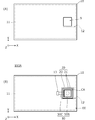
- FIG. 1A is a plan view of the circuit board 10, the coil antenna module 20, and the camera module 50 included in the antenna device according to the first embodiment
- FIG. 1B is a plan view of the antenna device 101
- FIG. 1C is a cross-sectional view of the electronic apparatus 201 including the antenna device 101
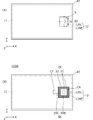
- 2A is a plan view of a coil antenna module included in the antenna device according to the second embodiment
- FIG. 2B is a plan view of the antenna device 102A according to the second embodiment
- FIG. 6C is a cross-sectional view of an electronic device 202A including the antenna device 102A.
- FIG. 3A is a plan view of another antenna device 102B according to the second embodiment
- FIG. 3B is a cross-sectional view of an electronic apparatus 202B including the antenna device 102B.
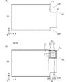
- 4A is a plan view of the circuit board 10 included in the antenna device according to the third embodiment, and FIG. 4B is a plan view of the antenna device 103A.
- FIG. 5A is a plan view of a circuit board 10 included in another antenna device according to the third embodiment, and FIG. 5B is a plan view of the antenna device 103B.
- FIG. 6A is a plan view of a circuit board included in still another antenna device according to the third embodiment, and FIG. 6B is a plan view of the antenna device 103C.
- FIG. 7A is a plan view of a circuit board included in still another antenna device according to the third embodiment, and FIG.
- FIG. 7B is a plan view of the antenna device 103D.
- FIG. 8 is a plan view of the antenna device 104 according to the fourth embodiment.
- FIG. 9A is a plan view of a circuit board included in the antenna device according to the fifth embodiment, and FIG. 9B is a plan view of the antenna device 105.
- FIG. 10A is a plan view of a circuit board included in the antenna device according to the sixth embodiment, and FIG. 10B is a plan view of the antenna device 106.
- the “antenna device” shown in each embodiment can be applied to either a signal (or power) transmission (power transmission) side or a reception (power reception) side. Even when this “antenna device” is described as an antenna that radiates magnetic flux, the antenna device is not limited to being a magnetic flux generation source. Even when the transmission counterpart antenna device receives (links) the generated magnetic flux, that is, even if the transmission / reception relationship is reversed, the same effect is obtained.
- the “antenna device” shown in the following embodiments is an antenna device used for near-field communication using magnetic field coupling with a communication partner antenna device, or a near field using magnetic coupling with a power transmission counterpart antenna device. It is an antenna apparatus used for the electric power transmission in.
- the present invention is applied to a communication system such as NFC (Near field communication).
- a power transmission system such as an electromagnetic induction method or a magnetic field resonance method.
- the “antenna device” shown in each embodiment is used in a wireless transmission system such as communication or power transmission using at least magnetic coupling.
- the “antenna device” shown in each embodiment includes a device that wirelessly transmits substantially by electromagnetic field coupling (magnetic field coupling and electric field coupling) with the transmission-side antenna device.
- the “antenna device” shown in each embodiment uses, for example, an HF band, particularly 13.56 MHz, 6.78 MHz, or a frequency band in the vicinity thereof.
- -HF band 3 MHz or more and 30 MHz or less-UHF band: 300 MHz or more and 3 GHz or less-SHF band: 3 GHz or more and 30 GHz or less Size of antenna device (typically from one end of a coil conductor pattern of a coil antenna included in the antenna device The length along the coil conductor to the end) is sufficiently smaller than the wavelength ⁇ at the used frequency, and the radiation efficiency of electromagnetic waves is low in the used frequency band. More specifically, the length of the current path of the antenna device is ⁇ / 10 or less. Thus, if the wavelength is sufficiently shorter than the wavelength in the operating frequency band, the current generated in the coil conductor is hardly distributed on the coordinate axis along the coil conductor, and a substantially constant current flows.
- the wavelength here is an effective wavelength in consideration of the wavelength shortening effect due to the dielectric property and magnetic permeability of the base material on which the coil conductor pattern is formed.
- a power feeding circuit for operating a signal (power) in the above-described frequency band is connected to both ends of the coil conductor pattern of the coil antenna.
- the coil conductor pattern of the coil antenna and the power supply circuit may be connected by magnetic field coupling via a power supply coil or a transformer (including a balun). In that case, both ends of the coil conductor included in the power supply coil or the transformer are connected to the power supply circuit, and both ends of the coil conductor included in the coil antenna are connected directly or via a capacitor.
- FIG. 1A is a plan view of the circuit board 10, the coil antenna module 20, and the camera module 50 included in the antenna device according to the first embodiment
- FIG. 1B is a plan view of the antenna device 101
- FIG. 1C is a cross-sectional view of the electronic apparatus 201 including the antenna device 101. In FIG. 1B, it is shown in a state where the casing portion is removed.
- FIG. 1C is a cross-sectional view of the electronic device taken along line XX in FIG.
- the electronic device 201 is, for example, a smartphone or a mobile phone terminal.
- the electronic apparatus 201 including the antenna device 101 includes the circuit board 10 in a casing including a rear casing 61 and a display casing 62, as shown in FIG.
- the coil antenna module 20 is affixed to the inner surface of the housing 61 on the back side.
- the main body 50B of the camera module 50 is attached to the housing 61 on the back side. A part of the camera module 50 is accommodated in the notch of the circuit board 10.
- the camera module 50 is an example of the “functional component” according to the present invention.
- the circuit board 10 is formed with a ground conductor pattern 11 extending in a planar shape.
- the ground conductor pattern 11 corresponds to a “planar conductor” according to the present invention.
- a cutout 12 having an outer edge EE is formed in the ground conductor pattern 11.
- a connector 13 for connecting the camera module 50 is mounted on the circuit board 10. The various components mounted on the circuit board are not shown in FIG.
- the coil antenna module 20 includes a coil antenna substrate 22 and a coil conductor pattern 21.
- the coil antenna substrate 22 is a rectangular annular flexible substrate, and a rectangular spiral coil conductor pattern 21 is formed on the coil antenna substrate 22.
- the coil conductor pattern 21 corresponds to a “coil antenna” according to the present invention.
- the camera module 50 includes a main body 50B and a cable 50C drawn from the main body 50B.
- the cable 50 ⁇ / b> C is drawn out in a direction not intersecting with the outer edge EE in a plan view of the ground conductor pattern 11 (that is, a direction not extending from the ground conductor formation region to the outside thereof).
- the cable 50C is pulled out from the main body 50B (in the ⁇ X direction).
- the coil opening CA of the coil conductor pattern 21 overlaps the notch 12 in a plan view of the ground conductor pattern 11.
- three sides of the rectangular spiral coil conductor pattern are along the edge of the notch 12 of the ground conductor pattern 11.
- the main body 50 ⁇ / b> B of the camera module 50 also overlaps the notch 12 in a plan view of the ground conductor pattern 11. Therefore, the coil conductor pattern 21 has a structure wound around the body 50B of the camera module 50.
- the cable 50C of the camera module 50 is electrically connected by being inserted into the connector 13.
- the ground conductor pattern 11 and the coil conductor pattern 21 of the coil antenna module 20 are electromagnetically coupled (electric field coupling and magnetic field coupling), in particular, magnetic field coupling.
- a current is induced in the ground conductor pattern 11, but the current density varies depending on the position of the ground conductor pattern 11.
- the magnetic flux generated by the current flowing through the ground conductor pattern 11 is concentrated particularly on the outer edge EE of the notch 12. That is, the magnetic flux density near the notch 12 is high.
- the cable 50C of the camera module 50 is drawn out so as not to cross the portion with the high magnetic flux density, so that the cable 50C is not easily affected by magnetic flux generated from the ground conductor pattern 11 and the coil conductor pattern 21. .
- the portion where the notch 12 is open is the high magnetic flux density portion HD, it is more preferable that the cable 50C is pulled out from the main body 50B in a direction away from the high magnetic flux density portion HD ( ⁇ X direction).
- the operational trouble of the camera module is suppressed.
- unnecessary coupling between the coil conductor pattern 21 and the cable 50C is suppressed, the characteristics of the coil antenna are hardly affected by the camera module 50.
- Second Embodiment the configuration of the coil antenna module will be described with respect to an antenna device and an electronic device that are different from those shown in the first embodiment.
- FIG. 2A is a plan view of a coil antenna module included in the antenna device according to the second embodiment
- FIG. 2B is a plan view of the antenna device 102A according to the second embodiment
- FIG. 6C is a cross-sectional view of an electronic device 202A including the antenna device 102A. In FIG. 2 (B), the case portion is excluded.
- FIG. 2C is a cross-sectional view of the electronic device taken along line XX in FIG.
- the electronic device 202A is, for example, a smartphone or a mobile phone terminal.
- the coil conductor pattern 21 and the cable 50C overlap each other between the coil conductor pattern 21 and the ground conductor pattern 11 of the coil antenna module 20 in a plan view of the ground conductor pattern 11.
- the magnetic body 23 is included.
- Other configurations are the same as those of the antenna device 101 shown in the first embodiment.
- the magnetic body 23 is, for example, a ferrite sheet, and is attached to the lower surface of the coil antenna module 20 at a position along the side from which the cable 50C is drawn through an adhesive sheet.
- the antenna device 102A unnecessary magnetic coupling between the coil conductor pattern 21 and the cable 50C of the camera module 50 is suppressed by the magnetic body 23. Further, the coil conductor pattern 21 has a portion facing the ground conductor pattern 11 without using the magnetic body 23. Thereby, the required coupling
- FIG. 3A is a plan view of another antenna device 102B according to the second embodiment
- FIG. 3B is a cross-sectional view of an electronic apparatus 202B including the antenna device 102B.
- the ground conductor pattern 21 is at least overlapped with the coil conductor pattern 21 and the cable 50 ⁇ / b> C in the plan view of the ground conductor pattern 11 between the coil conductor pattern 21 and the ground conductor pattern 11.
- 11 is provided with a conductive member 24 having a smaller area than 11.
- the conductive member 24 is a metal sheet having the same size as the magnetic body 23 and is attached so as to overlap the magnetic body 23.
- Other configurations are the same as those of the antenna device 102A illustrated in FIGS.
- the conductive member 24 is provided between the coil conductor pattern 21 and the ground conductor pattern 11 at the portion where the coil conductor pattern 21 and the cable 50 ⁇ / b> C overlap. Unnecessary electromagnetic coupling with the cable 50C is suppressed.
- the magnetic body 23 is provided, and the magnetic body 23 and the conductive member 24 are arranged in this order between the coil conductor pattern 21 and the ground conductor pattern 11. ing. Therefore, the coil conductor pattern 21 and the cable 50C are electromagnetically coupled to each other via the magnetic flux interlinking with the coil conductor pattern 21 while suppressing the decrease in the magnetic flux interlinking with the coil conductor pattern 21 due to the conductive member 24. To suppress.
- FIG. 4A is a plan view of the circuit board 10 included in the antenna device according to the third embodiment
- FIG. 4B is a plan view of the antenna device 103A.
- the notch 12 of the ground conductor pattern 11 is deep in the notch direction ( ⁇ X direction).
- a circuit board opening 9 for inserting the camera module 50 is also formed.
- FIG. 5A is a plan view of a circuit board 10 included in another antenna device according to the third embodiment
- FIG. 5B is a plan view of the antenna device 103B.
- a cutout 12 is formed in the ground conductor pattern 11 by an opening 12AP and a slit 12SL.
- the four sides of the rectangular spiral coil conductor pattern 21 are along the outer edge of the opening 12AP of the ground conductor pattern 11. Therefore, the coil conductor pattern 21 and the ground conductor pattern 11 are more strongly electromagnetically coupled (particularly magnetic field coupling).
- FIG. 6A is a plan view of a circuit board included in still another antenna device according to the third embodiment
- FIG. 6B is a plan view of the antenna device 103C.
- notches 12 are formed at the corners of the ground conductor pattern 11.
- the ground conductor pattern 11 is formed with a notch 12 having an outer edge EE.
- the coil antenna module 20 is arranged such that two sides of the rectangular spiral coil conductor pattern 21 are along the outer edge EE of the notch 12 of the ground conductor pattern 11.
- the magnetic flux generated by the current flowing through the ground conductor pattern 11 in combination with the coil conductor pattern 21 is concentrated particularly on the outer edge EE of the notch 12.
- the cable 50 ⁇ / b> C of the camera module 50 is drawn in a direction that does not intersect (do not straddle) the outer edge EE in a plan view of the ground conductor pattern 11.
- the cable 50C is pulled out from the main body 50B (in the ⁇ X direction). Therefore, the cable 50 ⁇ / b> C is less susceptible to magnetic flux interference generated from the ground conductor pattern 11 and the coil conductor pattern 21.
- the coil conductor pattern may be arranged at the corner of the ground conductor pattern 11.
- FIG. 7A is a plan view of a circuit board included in still another antenna device according to the third embodiment
- FIG. 7B is a plan view of the antenna device 103D.
- a circuit board notch 12A is formed at one corner of the circuit board 10, and a notch 12 is formed at the corner of the ground conductor pattern 11. As shown in FIG. Further, unlike the example shown in FIG. 6A, a notch 12B of the circuit board is formed at another corner.
- Other configurations are the same as those of the antenna device 103C illustrated in FIGS.
- FIG. 8 is a plan view of the antenna device 104 according to the fourth embodiment. Unlike the antenna device 101 shown in FIG. 1A, the cable 50C of the camera module 50 is drawn in the ⁇ Y direction. The shape of the notch 12 of the ground conductor pattern 11 is the same as that shown in the first embodiment.
- the direction in which the cable 50C is drawn from the main body 50B of the camera module 50 is a direction that does not intersect (do not straddle) the outer edge EE of the notch 12 in plan view of the ground conductor pattern 11.
- the direction in which the cable 50C is drawn from the main body 50B of the camera module 50 is drawn in a direction that does not intersect (does not straddle) the outer edge EE of the notch 12 in plan view of the ground conductor pattern 11. It only has to be.
- FIG. 9A is a plan view of a circuit board included in the antenna device according to the fifth embodiment
- FIG. 9B is a plan view of the antenna device 105.
- the ground conductor pattern 11 is formed on a part of the circuit board 10.
- a circuit board opening 9 for inserting the camera module 50 is also formed.
- a cutout 12 having an outer edge EE is formed in the ground conductor pattern 11 along the circuit board opening 9.
- the coil antenna module 20 is arranged such that two sides of the rectangular spiral coil conductor pattern 21 are along the outer edge EE of the notch 12 of the ground conductor pattern 11.
- the cable 50 ⁇ / b> C of the camera module 50 is drawn out in a direction not intersecting (stranding) the outer edge EE in the plan view of the ground conductor pattern 11.
- the cable 50C is pulled out from the main body 50B (in the ⁇ X direction). Therefore, the cable 50 ⁇ / b> C is less susceptible to magnetic flux interference generated from the ground conductor pattern 11 and the coil conductor pattern 21.
- the circuit board opening 9 is formed at a position near the lower side of the circuit board 10, but the circuit board opening 9 is formed near the center of the circuit board. It can be applied in the same way.
- the present invention can also be applied to a structure in which the planar conductor (ground conductor pattern 11) does not reach the outer edge of the circuit board. That is, when there is a planar conductor (ground conductor pattern) formation region and a non-formation region around the functional component (camera module 50), the cable 50C of the camera module 50 goes from the non-formation region of the planar conductor to the formation region. It only has to be pulled out.
- FIG. 10A is a plan view of a circuit board included in the antenna device according to the sixth embodiment
- FIG. 10B is a plan view of the antenna device 106.
- a circuit board notch 12 ⁇ / b> A is formed at one corner of the circuit board 10
- a circuit board notch 12 ⁇ / b> B is formed near another corner of the circuit board 10. Is formed.
- the area of the notch 12B of the circuit board 10 is smaller than the area of the notch 12A.
- the camera module 50 is a dual camera module including two optical components and an imaging unit.
- the vertical and horizontal dimensions of the coil conductor pattern 21 and the coil antenna substrate 22 of the coil antenna module 20 are dimensions corresponding to the size of the main body 50B of the camera module 50.
- a jack or a connector provided inside the housing or the inside of the housing is disposed at the position of the notch 12B of the circuit board, and the jack or the connector and the circuit board 10 are configured not to interfere with each other in structure. ing.
- a camera module is given as an example of a functional component.
- an optical component such as a camera module, a flash, an infrared sensor, or a display may be used.
- the functional component may be an operation component such as a pressing switch.
- input / output components such as a speaker, a microphone, a vibration motor, an actuator, and a connector may be used.
- the ground conductor pattern 11 formed on the circuit board is shown as an example of the planar conductor.
- a shield case or the like attached to the circuit board may be used as the “planar conductor”. Good.
- planar planar conductor ground conductor pattern 11
- shape of this planar conductor is not limited to planar, and may be curved. A part may be curved.
- the shape of the cutout is not limited to the shape as in each of the above-described embodiments as long as it is provided at a position where a functional component such as a camera module is inserted.
- the shape may also be
- the antenna device and the electronic device in the communication system mainly using the magnetic field coupling such as NFC have been described.
- the antenna device and the electronic device in the above-described embodiment use the magnetic field coupling.
- the contactless power transmission system (electromagnetic induction system, magnetic field resonance system, etc.) can be used similarly.
- the antenna device in the above-described embodiment can be applied as a power receiving antenna device to a power receiving device of a magnetic resonance type non-contact power transmission system used in the HF band, particularly in the vicinity of 6.78 MHz or 6.78 MHz. Even in this case, the antenna device functions as a power receiving antenna device.
- the “power feeding circuit” shown in the above embodiment corresponds to a power receiving circuit or a power transmitting circuit.
- the power receiving antenna device is connected to supply power to a load (for example, a secondary battery).
- the power transmission antenna device is connected to supply power to the power transmission antenna device.
- the power receiving circuit includes a rectifier circuit that is connected to the coil antenna and the load, converts electric power from the coil antenna into a direct current, and supplies the direct current to the load. Further, it may further include a smoothing circuit, a DC-DC converter circuit, and the like.
- the power transmission circuit includes an inverter circuit that supplies power to the coil antenna.
Landscapes
- Engineering & Computer Science (AREA)
- Signal Processing (AREA)
- Support Of Aerials (AREA)
- Details Of Aerials (AREA)
- Telephone Set Structure (AREA)
- Aerials With Secondary Devices (AREA)
Description
本発明は、電子機器の筐体内に収納される、または電子機器の筐体を一部に含む、アンテナ装置に関する。
筐体の金属部等の、開口を有する面状導体と、コイルアンテナとを備え、面状導体にコイル開口を重ねることで、コイルアンテナと面状導体とを結合させ、面状導体をブースターとして利用したアンテナ装置が特許文献1に示されている。また、特許文献1には、上記開口の位置にカメラモジュールを配置することが示されている。
コイルアンテナと結合する面状導体は、回路基板に形成されたグランド導体や回路基板に固定されたシールドケース等であってもよい。しかし、カメラモジュールから引き出されているケーブルが回路基板に接続される場合、面状導体の主面の法線方向において、ケーブルがコイルアンテナと面状導体との間に位置するため、そのケーブルが面状導体やコイル導体から発生する磁束の干渉を受けやすい。このカメラモジュールのケーブルが受ける干渉は、例えば、画像信号にノイズ成分が重畳される等、カメラモジュールの動作上の障害となる場合があることを本発明の発明者は見出した。このような動作上の障害はカメラモジュールに限らず、コイルアンテナと面状導体とを含み、機能部品と共に構成されるアンテナ装置に共通の解決すべき課題である。
本発明の目的は、コイルアンテナと面状導体とを含み、機能部品と共に構成されるアンテナ装置において、上記機能部品のケーブルが受ける干渉の問題を解消したアンテナ装置およびそれを備える電子機器を提供することにある。
(1)本発明のアンテナ装置は、
回路基板と、
前記回路基板に設けられ、外縁を有する切り欠きが形成された面状導体と、
本体、および当該本体から引き出され前記回路基板に接続されるケーブルを有し、前記面状導体の平面視で前記本体が前記切り欠きに重なる、機能部品と、
前記機能部品の前記本体の周囲に巻回されたコイル導体で構成されるコイルアンテナと、
を備え、
前記ケーブルは前記コイルアンテナと前記面状導体との間に位置し、
前記機能部品の本体からの前記ケーブルの引き出し方向は、前記面状導体の平面視で前記外縁と交差しない方向である、ことを特徴とする。
回路基板と、
前記回路基板に設けられ、外縁を有する切り欠きが形成された面状導体と、
本体、および当該本体から引き出され前記回路基板に接続されるケーブルを有し、前記面状導体の平面視で前記本体が前記切り欠きに重なる、機能部品と、
前記機能部品の前記本体の周囲に巻回されたコイル導体で構成されるコイルアンテナと、
を備え、
前記ケーブルは前記コイルアンテナと前記面状導体との間に位置し、
前記機能部品の本体からの前記ケーブルの引き出し方向は、前記面状導体の平面視で前記外縁と交差しない方向である、ことを特徴とする。
上記面状導体はコイルアンテナのコイル導体と結合することにより電流が流れるが、電流密度は面状導体の位置により異なる。この面状導体に電流が流れることにより生じる磁束は、特に切り欠きの外縁に集中する。すなわち、切り欠きの外縁近傍の磁束密度は高い。上記構成により、機能部品のケーブルは上記磁束密度の高い部分を避ける方向に引き出されているので、そのケーブルは面状導体やコイル導体から発生する磁束の干渉を受け難い。
(2)例えば、前記面状導体は前記回路基板に形成されたグランド導体である。そのことにより、アンテナ装置専用の面状導体を形成する必要がなく、小型の電子機器でありながら、実効的なアンテナ面積の大きなアンテナ装置を設けることができる。
(3)前記コイルアンテナと前記面状導体との間に配置され、前記面状導体の平面視で、少なくとも前記コイル導体と前記ケーブルとが重なる部分に磁性体をさらに備えることが好ましい。これにより、コイル導体と機能部品のケーブルとの不要な磁界結合が抑制される。
(4)前記コイル導体は、前記磁性体を介さずに前記面状導体と対向する部分を有することが好ましい。これにより、コイルアンテナと面状導体との必要な結合が確保され、面状導体が存在することによる放射特性向上効果が維持される。
(5)前記コイルアンテナと前記面状導体との間に配置され、前記面状導体の平面視で、少なくとも前記コイル導体と前記ケーブルとが重なる部分に、前記面状導体よりも小面積の導電性部材を備えることが好ましい。これにより、コイル導体と機能部品のケーブルとの不要な電磁界結合が抑制される。
(6)前記コイルアンテナと前記面状導体との間に配置され、前記面状導体の平面視で、少なくとも前記コイル導体と前記ケーブルとが重なる部分に、前記面状導体よりも小面積の導電性部材および磁性体を備え、前記導電性部材が前記磁性体と前記面状導体との間に配置されることが好ましい。このことにより、導電性部材に起因する、コイル導体に鎖交する磁束の低下を抑制しつつ、コイル導体に鎖交する磁束を介してコイル導体とケーブルとが電磁界結合することを抑制する。
(7)前記機能部品は、例えば、カメラモジュール、フラッシュ、赤外センサ、ディスプレイ等の光学部品であってもよい。
(8)前記機能部品は押圧操作のスイッチ等の操作部品であってもよい。
(9)本発明の電子機器は、筐体に収納されるアンテナ装置を備え、
前記アンテナ装置は、
回路基板と、
前記回路基板に設けられ、外縁を有する切り欠きが形成された面状導体と、
本体、および当該本体から引き出され前記回路基板に接続されるケーブルを有し、前記面状導体の平面視で前記本体が前記切り欠きに重なる、機能部品と、
前記機能部品の前記本体の周囲に巻回されたコイル導体で構成されるコイルアンテナと、
を備え、
前記ケーブルは前記コイルアンテナと前記面状導体との間に位置し、
前記機能部品の本体からの前記ケーブルの引き出し方向は、前記面状導体の平面視で前記外縁と交差しない方向である、ことを特徴とする。
前記アンテナ装置は、
回路基板と、
前記回路基板に設けられ、外縁を有する切り欠きが形成された面状導体と、
本体、および当該本体から引き出され前記回路基板に接続されるケーブルを有し、前記面状導体の平面視で前記本体が前記切り欠きに重なる、機能部品と、
前記機能部品の前記本体の周囲に巻回されたコイル導体で構成されるコイルアンテナと、
を備え、
前記ケーブルは前記コイルアンテナと前記面状導体との間に位置し、
前記機能部品の本体からの前記ケーブルの引き出し方向は、前記面状導体の平面視で前記外縁と交差しない方向である、ことを特徴とする。
上記構成により、機能部品のケーブルが面状導体やコイル導体から発生する磁束の干渉を受け難く、機能部品の動作上の障害が抑制されるので、機能部品とともにアンテナ装置が筐体内に高密度に実装される電子機器が得られる。
本発明によれば、機能部品のケーブルが受ける干渉の問題を解消したアンテナ装置およびそれを備える電子機器が構成できる。
以降、図を参照して幾つかの具体的な例を挙げて、本発明を実施するための複数の形態を示す。各図中には同一箇所に同一符号を付している。要点の説明または理解の容易性を考慮して、便宜上実施形態を分けて示すが、異なる実施形態で示した構成の部分的な置換または組み合わせは可能である。第2の実施形態以降では第1の実施形態と共通の事柄についての記述を省略し、異なる点についてのみ説明する。特に、同様の構成による同様の作用効果については実施形態毎には逐次言及しない。
各実施形態に示す「アンテナ装置」は、信号(または電力)の送信(送電)側、受信(受電)側のいずれにも適用できる。この「アンテナ装置」を、磁束を放射するアンテナとして説明する場合でも、そのアンテナ装置が磁束の発生源であることに限るものではない。伝送相手側アンテナ装置が発生した磁束を受ける(鎖交する)場合にも、すなわち送受の関係が逆であっても、同様の作用効果を奏する。
以降の各実施形態に示す「アンテナ装置」は、通信相手側アンテナ装置と磁界結合を用いた近傍界通信のために用いられるアンテナ装置、または電力伝送相手側アンテナ装置と磁界結合を用いた近傍界での電力伝送のために用いられるアンテナ装置である。通信の場合には、例えばNFC(Near field communication)等の通信システムに適用される。電力伝送の場合には、例えば電磁誘導方式や磁界共鳴方式等の電力伝送システムに適用される。つまり、各実施形態に示す「アンテナ装置」は、少なくとも磁界結合を利用した通信や電力伝送等の無線伝送システムで用いられる。なお、各実施形態に示す「アンテナ装置」は、実質的に伝送相手側アンテナ装置と電磁界結合(磁界結合および電界結合)により無線伝送しているものも含む。
各実施形態に示す「アンテナ装置」は、例えばHF帯、特に13.56MHz、6.78MHzまたはそれらの近傍の周波数帯が利用される。
ここで、各周波数帯の数値範囲は例えば次のように表すことができる。
・HF帯:3MHz以上30MHz以下
・UHF帯:300MHz以上3GHz以下
・SHF帯:3GHz以上30GHz以下
アンテナ装置の大きさ(典型的には、アンテナ装置が備えるコイルアンテナが有するコイル導体パターンの一端から他端までコイル導体に沿った長さ)は、使用する周波数における波長λに比べて十分に小さく、使用周波数帯においては電磁波の放射効率は低い。より具体的には、アンテナ装置の電流経路の長さはλ/10以下である。このように、使用周波数帯での波長に比較して十分に短いと、コイル導体に生じる電流の、コイル導体に沿った座標軸での分布はほとんど生じず、ほぼ一定の大きさの電流が流れる。なお、ここでいう波長とは、コイル導体パターンが形成される基材の誘電性や透磁性による波長短縮効果を考慮した実効的な波長である。
・UHF帯:300MHz以上3GHz以下
・SHF帯:3GHz以上30GHz以下
アンテナ装置の大きさ(典型的には、アンテナ装置が備えるコイルアンテナが有するコイル導体パターンの一端から他端までコイル導体に沿った長さ)は、使用する周波数における波長λに比べて十分に小さく、使用周波数帯においては電磁波の放射効率は低い。より具体的には、アンテナ装置の電流経路の長さはλ/10以下である。このように、使用周波数帯での波長に比較して十分に短いと、コイル導体に生じる電流の、コイル導体に沿った座標軸での分布はほとんど生じず、ほぼ一定の大きさの電流が流れる。なお、ここでいう波長とは、コイル導体パターンが形成される基材の誘電性や透磁性による波長短縮効果を考慮した実効的な波長である。
コイルアンテナが有するコイル導体パターンの両端には、上記使用周波数帯の信号(電力)を操作する給電回路が接続される。なお、コイルアンテナが有するコイル導体パターンと給電回路とは、給電コイルやトランス(バラン含む)を介して磁界結合により接続されてもよい。その場合は、給電コイルやトランスが有するコイル導体の両端が給電回路に接続され、コイルアンテナが有するコイル導体の両端が互いに直接またはキャパシタを介して接続される。
《第1の実施形態》
図1(A)は第1の実施形態に係るアンテナ装置が有する回路基板10、コイルアンテナモジュール20およびカメラモジュール50の平面図であり、図1(B)は、そのアンテナ装置101の平面図であり、図1(C)は、アンテナ装置101を備える電子機器201の断面図である。図1(B)では筐体部分を除いた状態で表している。図1(C)は、図1(B)におけるX-X部分での電子機器の断面図である。電子機器201は例えばスマートフォンや携帯電話端末である。
図1(A)は第1の実施形態に係るアンテナ装置が有する回路基板10、コイルアンテナモジュール20およびカメラモジュール50の平面図であり、図1(B)は、そのアンテナ装置101の平面図であり、図1(C)は、アンテナ装置101を備える電子機器201の断面図である。図1(B)では筐体部分を除いた状態で表している。図1(C)は、図1(B)におけるX-X部分での電子機器の断面図である。電子機器201は例えばスマートフォンや携帯電話端末である。
このアンテナ装置101を備える電子機器201は、図1(C)に表れているように、背面側の筐体61およびディスプレイ側の筐体62を含む筐体内に回路基板10を備える。
背面側の筐体61の内面にはコイルアンテナモジュール20が貼付されている。また、背面側の筐体61にカメラモジュール50の本体50Bが取り付けられている。カメラモジュール50の一部は回路基板10の切り欠き内に収まっている。カメラモジュール50は本発明に係る「機能部品」の一例である。
図1(A)に表れているように、回路基板10には、面状に拡がるグランド導体パターン11が形成されている。このグランド導体パターン11は本発明に係る「面状導体」に相当する。グランド導体パターン11には、外縁EEを有する切り欠き12が形成されている。また、回路基板10にはカメラモジュール50を接続するコネクタ13が実装されている。回路基板に実装される各種部品については、図1(A)においては図示を省略している。
また、図1(A)に表れているように、コイルアンテナモジュール20は、コイルアンテナ基板22とコイル導体パターン21とで構成されている。コイルアンテナ基板22は矩形環状のフレキシブル基板であり、このコイルアンテナ基板22に、矩形スパイラル状のコイル導体パターン21が形成されている。このコイル導体パターン21は本発明に係る「コイルアンテナ」に相当する。
さらに、図1(A)に表れているように、カメラモジュール50は本体50Bとこの本体50Bから引き出されたケーブル50Cを備えている。ケーブル50Cは、グランド導体パターン11の平面視で、外縁EEと交差しない方向(すなわち、グランド導体形成領域からその外側へ跨がない方向)に引き出されている。この例では、ケーブル50Cは(-X方向)に本体50Bから引き出されている。
図1(B)に表れているように、コイル導体パターン21のコイル開口CAは、グランド導体パターン11の平面視で、切り欠き12に重なる。この例では、矩形スパイラル状のコイル導体パターンの3辺がグランド導体パターン11の切り欠き12の縁に沿っている。また、グランド導体パターン11の平面視で、カメラモジュール50の本体50Bも切り欠き12に重なる。したがって、コイル導体パターン21はカメラモジュール50の本体50Bの周囲に巻回された構造である。カメラモジュール50のケーブル50Cはコネクタ13に差し込まれることにより電気的に接続される。
グランド導体パターン11はコイルアンテナモジュール20のコイル導体パターン21と電磁界結合(電界結合および磁界結合)、特に磁界結合する。このことにより、グランド導体パターン11に電流が誘導されるが、電流密度はグランド導体パターン11の位置により異なる。このグランド導体パターン11に電流が流れることにより生じる磁束は、特に切り欠き12の外縁EEに集中する。すなわち、切り欠き12近傍の磁束密度は高い。
上記構成により、カメラモジュール50のケーブル50Cは上記磁束密度の高い部分を交差しないように引き出されているので、そのケーブル50Cはグランド導体パターン11やコイル導体パターン21から発生する磁束の干渉を受け難い。特に、切り欠き12が開いている箇所は高磁束密度部分HDであるので、ケーブル50Cがこの高磁束密度部分HDから遠ざかる方向(-X方向)に本体50Bから引き出されていることはより好ましい。
上述の作用により、本実施形態によればカメラモジュールの動作上の障害は抑制される。また、コイル導体パターン21とケーブル50Cとの不要結合も抑制されるので、コイルアンテナの特性についてもカメラモジュール50の影響を受けにくい。
《第2の実施形態》
第2の実施形態では、コイルアンテナモジュールの構成が、第1の実施形態で示したものと異なるアンテナ装置および電子機器について示す。
第2の実施形態では、コイルアンテナモジュールの構成が、第1の実施形態で示したものと異なるアンテナ装置および電子機器について示す。
図2(A)は第2の実施形態に係るアンテナ装置が有するコイルアンテナモジュールの平面図であり、図2(B)は第2の実施形態に係るアンテナ装置102Aの平面図であり、図2(C)は、アンテナ装置102Aを備える電子機器202Aの断面図である。図2(B)では筐体部分を除いた状態で表している。図2(C)は、図2(B)におけるX-X部分での電子機器の断面図である。電子機器202Aは例えばスマートフォンや携帯電話端末である。
本実施形態のアンテナ装置102Aにおいては、コイルアンテナモジュール20のコイル導体パターン21とグランド導体パターン11との間に、グランド導体パターン11の平面視で、コイル導体パターン21とケーブル50Cとの重なる部分に、磁性体23を有する。その他の構成は第1の実施形態で示したアンテナ装置101と同じである。
上記磁性体23は例えばフェライトシートであり、コイルアンテナモジュール20の下面のうち、ケーブル50Cが引き出される辺に沿う位置に、粘着シートを介して貼付されている。
上記アンテナ装置102Aにおいては、コイル導体パターン21とカメラモジュール50のケーブル50Cとの不要な磁界結合が、磁性体23によって抑制される。また、コイル導体パターン21は、磁性体23を介さずにグランド導体パターン11と対向する部分を有する。これにより、コイル導体パターン21とグランド導体パターン11との必要な結合が確保され、グランド導体パターン11による放射特性向上効果が維持される。
図3(A)は第2の実施形態に係る別のアンテナ装置102Bの平面図であり、図3(B)はアンテナ装置102Bを備える電子機器202Bの断面図である。本実施形態のアンテナ装置102Bにおいては、コイル導体パターン21とグランド導体パターン11との間に、グランド導体パターン11の平面視で、少なくともコイル導体パターン21とケーブル50Cとが重なる部分に、グランド導体パターン11よりも小面積の導電性部材24を備える。
この例では、上記導電性部材24は磁性体23と同サイズの金属シートであり、磁性体23に重なるように貼付されている。その他の構成は図2(A)(B)に示したアンテナ装置102Aと同じである。
アンテナ装置102Bによれば、コイル導体パターン21とグランド導体パターン11との間に、コイル導体パターン21とケーブル50Cとが重なる部分に導電性部材24を備えるので、コイル導体パターン21とカメラモジュール50のケーブル50Cとの不要な電磁界結合が抑制される。
また、図3(A)(B)に示した例では、磁性体23を備え、且つ、コイル導体パターン21からグランド導体パターン11までの間に、磁性体23、導電性部材24の順に配置されている。そのため、導電性部材24に起因する、コイル導体パターン21に鎖交する磁束の低下を抑制しつつ、コイル導体パターン21に鎖交する磁束を介してコイル導体パターン21とケーブル50Cとが電磁界結合することを抑制する。
《第3の実施形態》
第3の実施形態では、グランド導体パターンの切り欠きの形状およびコイルアンテナモジュールの配置位置が、第1の実施形態で示したものと異なるアンテナ装置について示す。
第3の実施形態では、グランド導体パターンの切り欠きの形状およびコイルアンテナモジュールの配置位置が、第1の実施形態で示したものと異なるアンテナ装置について示す。
図4(A)は第3の実施形態に係るアンテナ装置が有する回路基板10の平面図であり、図4(B)は、そのアンテナ装置103Aの平面図である。図1(A)に示したアンテナ装置101と比べると、グランド導体パターン11の切り欠き12は切り欠き方向(-X方向)に深い。また、カメラモジュール50を挿通させるための、回路基板開口9が形成されている。
図5(A)は第3の実施形態に係る別のアンテナ装置が有する回路基板10の平面図であり、図5(B)は、そのアンテナ装置103Bの平面図である。図4(B)に示したアンテナ装置103Aとは異なり、グランド導体パターン11に、開口12APおよびスリット12SLで切り欠き12が形成されている。矩形スパイラル状のコイル導体パターン21の4辺がグランド導体パターン11の開口12APの外縁に沿っている。そのため、コイル導体パターン21とグランド導体パターン11とは、より強く電磁界結合(特に磁界結合)する。
図6(A)は第3の実施形態に係る更に別のアンテナ装置が有する回路基板の平面図であり、図6(B)はそのアンテナ装置103Cの平面図である。
図6(A)に表れているように、グランド導体パターン11の角部に切り欠き12が形成されている。図6(A)において、グランド導体パターン11には、外縁EEを有する切り欠き12が形成されている。図6(B)に表れているように、コイルアンテナモジュール20は、矩形スパイラル状のコイル導体パターン21の2辺がグランド導体パターン11の切り欠き12の外縁EEに沿うように配置されている。
コイル導体パターン21と結合してグランド導体パターン11に電流が流れることにより生じる磁束は、特に切り欠き12の外縁EEに集中する。カメラモジュール50のケーブル50Cは、グランド導体パターン11の平面視で、外縁EEと交差しない(跨がない)方向に引き出されている。この例では、ケーブル50Cは(-X方向)に本体50Bから引き出されている。したがって、ケーブル50Cはグランド導体パターン11やコイル導体パターン21から発生する磁束の干渉を受け難い。
このように、コイル導体パターンをグランド導体パターン11の角部に配置してもよい。
図7(A)は第3の実施形態に係る更に別のアンテナ装置が有する回路基板の平面図であり、図7(B)はそのアンテナ装置103Dの平面図である。
図7(A)に表れているように、回路基板10の1つの角部に回路基板の切り欠き12Aが形成されて、グランド導体パターン11の角部に切り欠き12が形成されている。また、図6(A)に示した例とは異なり、別の角部に回路基板の切り欠き12Bが形成されている。その他の構成は図6(A)(B)に示したアンテナ装置103Cと同じである。
図7(A)(B)に示したように、回路基板の隣接する2つの角部に切り欠きがあってもよい。
《第4の実施形態》
第4の実施形態では、カメラモジュールのケーブル引出方向が、これまでに示した実施形態とは異なる例について示す。
第4の実施形態では、カメラモジュールのケーブル引出方向が、これまでに示した実施形態とは異なる例について示す。
図8は第4の実施形態に係るアンテナ装置104の平面図である。図1(A)に示したアンテナ装置101とは異なり、カメラモジュール50のケーブル50Cは-Y方向に引き出されている。グランド導体パターン11の切り欠き12の形状は第1の実施形態で示したものと同じである。
これまでの各実施形態で示したように、カメラモジュール50の本体50Bからのケーブル50Cの引き出し方向は、グランド導体パターン11の平面視で切り欠き12の外縁EEと交差しない(跨がない)方向に引き出されている。本実施形態で示すように、カメラモジュール50の本体50Bからのケーブル50Cの引き出し方向は、グランド導体パターン11の平面視で、切り欠き12の外縁EEと交差しない(跨がない)方向に引き出されていればよい。
《第5の実施形態》
第5の実施形態では、回路基板と面状導体の形状がこれまでに示した実施形態とは異なる例について示す。
第5の実施形態では、回路基板と面状導体の形状がこれまでに示した実施形態とは異なる例について示す。
図9(A)は第5の実施形態に係るアンテナ装置が有する回路基板の平面図であり、図9(B)はそのアンテナ装置105の平面図である。
図9(A)に表れているように、グランド導体パターン11は回路基板10の一部に形成されている。また、カメラモジュール50を挿通させるための、回路基板開口9が形成されている。グランド導体パターン11には、外縁EEを有する切り欠き12が、回路基板開口9に沿って形成されている。図9(B)に表れているように、コイルアンテナモジュール20は、矩形スパイラル状のコイル導体パターン21の2辺がグランド導体パターン11の切り欠き12の外縁EEに沿うように配置されている。
本実施形態においても、カメラモジュール50のケーブル50Cは、グランド導体パターン11の平面視で、外縁EEと交差しない(跨がない)方向に引き出されている。この例では、ケーブル50Cは(-X方向)に本体50Bから引き出されている。したがって、ケーブル50Cはグランド導体パターン11やコイル導体パターン21から発生する磁束の干渉を受け難い。
図9(A)、図9(B)に示した例では、回路基板開口9が回路基板10の下辺寄りの位置に形成されているが、回路基板開口9が回路基板の中央付近に形成されている場合にも同様に適用できる。
このように、面状導体(グランド導体パターン11)が回路基板の外縁に達していない構造においても、本発明は適用できる。すなわち、機能部品(カメラモジュール50)の周辺に面状導体(グランド導体パターン)形成領域と非形成領域とがある場合に、カメラモジュール50のケーブル50Cは面状導体の非形成領域から形成領域へ引き出されていればよい。
《第6の実施形態》
第6の実施形態では、回路基板と面状導体の形状がこれまでに示した実施形態とは異なる例について示す。
第6の実施形態では、回路基板と面状導体の形状がこれまでに示した実施形態とは異なる例について示す。
図10(A)は第6の実施形態に係るアンテナ装置が有する回路基板の平面図であり、図10(B)はそのアンテナ装置106の平面図である。
図10(A)に表れているように、回路基板10の1つの角部に回路基板の切り欠き12Aが形成されていて、回路基板10の別の角部付近に回路基板の切り欠き12Bが形成されている。回路基板10の平面視で、回路基板10の切り欠き12Bの面積は、切り欠き12Aの面積よりも小さい。
図10(B)において、カメラモジュール50は2つの光学部品および撮像部を備えるデュアルカメラのモジュールである。コイルアンテナモジュール20のコイル導体パターン21およびコイルアンテナ基板22の縦横の寸法は、カメラモジュール50の本体50Bのサイズに応じた寸法となっている。
なお、回路基板の切り欠き12Bの位置に、筐体または筐体の内側に設けられている例えばジャックやコネクタが配置されて、ジャックやコネクタと回路基板10とが構造上干渉しないように構成されている。
以上に示した各実施形態では機能部品の例としてカメラモジュールを挙げたが、例えば、カメラモジュール、フラッシュ、赤外センサ、ディスプレイ等の光学部品であってもよい。また、機能部品は押圧操作のスイッチ等の操作部品であってもよい。更には、スピーカー、マイク、振動モーター、アクチュエータ、コネクタ等の入出力部品であってもよい。
以上に示した各実施形態では、回路基板に形成されたグランド導体パターン11を面状導体の一例として示したが、回路基板に取り付けられたシールドケース等を「面状導体」に利用してもよい。
また、以上に示した各実施形態では、平面状の面状導体(グランド導体パターン11)を示したが、この面状導体の形状は平面状に限らず、曲面状であってもよいし、一部が曲面状であってもよい。
また、切り欠きの形状は、カメラモジュール等の機能部品を挿入する位置に設けられていればよく、以上に示した各実施形態のような形状に限られず、円形、楕円形、台形等の他の形状であってもよい。
なお、以上に示した各実施形態では、主にNFC等の磁界結合を利用した通信システムにおけるアンテナ装置および電子機器について説明したが、上述の実施形態におけるアンテナ装置および電子機器は、磁界結合を利用した非接触電力伝送システム(電磁誘導方式、磁界共鳴方式等)でも同様に用いることができる。例えば、上述の実施形態におけるアンテナ装置は、HF帯、特に6.78MHzまたは6.78MHz近傍の周波数で使用される磁界共鳴方式の非接触電力伝送システムの受電装置に受電アンテナ装置として適用できる。この場合でも、アンテナ装置は受電アンテナ装置として機能する。非接触電力伝送システムにおいては、上述の実施形態で示した「給電回路」は受電回路または送電回路に相当する。受電回路である場合は、受電アンテナ装置に接続され、負荷(例えば、二次電池)に電力を給電する。また、送電回路である場合は、送電アンテナ装置に接続され、送電アンテナ装置に電力を給電する。
上記受電回路には、コイルアンテナおよび負荷に接続されてコイルアンテナからの電力を直流に変換して負荷に供給する整流回路が含まれる。また、平滑回路やDC-DCコンバータ回路等を更に含んでもよい。また、送電回路はコイルアンテナに電力を供給するインバータ回路を含む。
最後に、上述の実施形態の説明は、すべての点で例示であって、制限的なものではない。当業者にとって変形および変更が適宜可能である。本発明の範囲は、上述の実施形態ではなく、特許請求の範囲によって示される。さらに、本発明の範囲には、特許請求の範囲内と均等の範囲内での実施形態からの変更が含まれる。
CA…コイル開口
EE…外縁
HD…高磁束密度部分
9…回路基板の開口
10…回路基板
11…グランド導体パターン
12…切り欠き
12AP…開口
12SL…スリット
12A,12B…回路基板の切り欠き
13…コネクタ
20…コイルアンテナモジュール
21…コイル導体パターン
22…コイルアンテナ基板
23…磁性体
24…導電性部材
50…カメラモジュール
50B…カメラモジュールの本体
50C…カメラモジュールのケーブル
61,62…筐体
101…アンテナ装置
102A,102B…アンテナ装置
103A,103B,103C…アンテナ装置
104,105…アンテナ装置
201,202A,202B…電子機器
EE…外縁
HD…高磁束密度部分
9…回路基板の開口
10…回路基板
11…グランド導体パターン
12…切り欠き
12AP…開口
12SL…スリット
12A,12B…回路基板の切り欠き
13…コネクタ
20…コイルアンテナモジュール
21…コイル導体パターン
22…コイルアンテナ基板
23…磁性体
24…導電性部材
50…カメラモジュール
50B…カメラモジュールの本体
50C…カメラモジュールのケーブル
61,62…筐体
101…アンテナ装置
102A,102B…アンテナ装置
103A,103B,103C…アンテナ装置
104,105…アンテナ装置
201,202A,202B…電子機器
Claims (9)
- 回路基板と、
前記回路基板に設けられ、外縁を有する切り欠きが形成された面状導体と、
本体、および当該本体から引き出され前記回路基板に接続されるケーブルを有し、前記面状導体の平面視で前記本体が前記切り欠きに重なる、機能部品と、
前記機能部品の前記本体の周囲に巻回されたコイル導体で構成されるコイルアンテナと、
を備え、
前記ケーブルは前記コイルアンテナと前記面状導体との間に位置し、
前記機能部品の本体からの前記ケーブルの引き出し方向は、前記面状導体の平面視で前記外縁と交差しない方向である、アンテナ装置。 - 前記面状導体は前記回路基板に形成されたグランド導体である、請求項1に記載のアンテナ装置。
- 前記コイルアンテナと前記面状導体との間に配置され、前記面状導体の平面視で、少なくとも前記コイル導体と前記ケーブルとが重なる部分に磁性体をさらに備える、請求項1または2に記載のアンテナ装置。
- 前記コイル導体は、前記磁性体を介さずに前記面状導体と対向する部分を有する、請求項3に記載のアンテナ装置。
- 前記コイルアンテナと前記面状導体との間に配置され、前記面状導体の平面視で、少なくとも前記コイル導体と前記ケーブルとが重なる部分に、前記面状導体よりも小面積の導電性部材を備える、請求項1から4のいずれかに記載のアンテナ装置。
- 前記コイルアンテナと前記面状導体との間に配置され、前記面状導体の平面視で、少なくとも前記コイル導体と前記ケーブルとが重なる部分に、前記面状導体よりも小面積の導電性部材および磁性体を備え、
前記導電性部材は、前記磁性体と前記面状導体との間に配置された、請求項1または2に記載のアンテナ装置。 - 前記機能部品は光学部品である、請求項1から6のいずれかに記載のアンテナ装置。
- 前記機能部品は操作部品である、請求項1から6のいずれかに記載のアンテナ装置。
- 筐体に収納されるアンテナ装置を備える電子機器であり、
前記アンテナ装置は、
回路基板と、
前記回路基板に設けられ、外縁を有する切り欠きが形成された面状導体と、
本体、および当該本体から引き出され前記回路基板に接続されるケーブルを有し、前記面状導体の平面視で前記本体が前記切り欠きに重なる、機能部品と、
前記機能部品の前記本体の周囲に巻回されたコイル導体で構成されるコイルアンテナと、
を備え、
前記ケーブルは前記コイルアンテナと前記面状導体との間に位置し、
前記機能部品の本体からの前記ケーブルの引き出し方向は、前記面状導体の平面視で前記外縁と交差しない方向である、ことを特徴とする電子機器。
Priority Applications (2)
| Application Number | Priority Date | Filing Date | Title |
|---|---|---|---|
| CN201790000761.4U CN209515981U (zh) | 2016-06-28 | 2017-04-14 | 天线装置以及电子设备 |
| JP2018524906A JP6380718B2 (ja) | 2016-06-28 | 2017-04-14 | アンテナ装置および電子機器 |
Applications Claiming Priority (2)
| Application Number | Priority Date | Filing Date | Title |
|---|---|---|---|
| JP2016127369 | 2016-06-28 | ||
| JP2016-127369 | 2016-06-28 |
Publications (1)
| Publication Number | Publication Date |
|---|---|
| WO2018003239A2 true WO2018003239A2 (ja) | 2018-01-04 |
Family
ID=60786380
Family Applications (1)
| Application Number | Title | Priority Date | Filing Date |
|---|---|---|---|
| PCT/JP2017/015270 Ceased WO2018003239A2 (ja) | 2016-06-28 | 2017-04-14 | アンテナ装置および電子機器 |
Country Status (3)
| Country | Link |
|---|---|
| JP (1) | JP6380718B2 (ja) |
| CN (2) | CN209515981U (ja) |
| WO (1) | WO2018003239A2 (ja) |
Cited By (1)
| Publication number | Priority date | Publication date | Assignee | Title |
|---|---|---|---|---|
| JP2021072612A (ja) * | 2019-10-31 | 2021-05-06 | 三星ディスプレイ株式會社Samsung Display Co.,Ltd. | 表示装置及びこれを含む電子機器 |
Families Citing this family (1)
| Publication number | Priority date | Publication date | Assignee | Title |
|---|---|---|---|---|
| CN112186324A (zh) * | 2020-09-16 | 2021-01-05 | 珠海格力电器股份有限公司 | 用于终端设备的天线组件和终端设备 |
Family Cites Families (10)
| Publication number | Priority date | Publication date | Assignee | Title |
|---|---|---|---|---|
| US20080268925A1 (en) * | 2007-04-27 | 2008-10-30 | Chia-Lun Tang | Antenna module for a mobile phone |
| CN103620868B (zh) * | 2012-02-01 | 2016-06-08 | 株式会社村田制作所 | 天线装置及通信终端装置 |
| JP5924006B2 (ja) * | 2012-02-02 | 2016-05-25 | 株式会社村田製作所 | アンテナ装置 |
| JP5834987B2 (ja) * | 2012-02-15 | 2015-12-24 | 株式会社村田製作所 | アンテナ装置および無線通信装置 |
| JP6183688B2 (ja) * | 2013-05-28 | 2017-08-23 | 日立金属株式会社 | アンテナ装置および無線通信装置 |
| JP2015043567A (ja) * | 2013-08-20 | 2015-03-05 | サムソン エレクトロ−メカニックス カンパニーリミテッド. | カメラモジュール及びそれを含む電子装置 |
| WO2015041066A1 (ja) * | 2013-09-17 | 2015-03-26 | 株式会社村田製作所 | カメラモジュールおよび電子機器 |
| WO2015163295A1 (ja) * | 2014-04-23 | 2015-10-29 | 株式会社村田製作所 | アンテナ装置および電子機器 |
| CN104993216A (zh) * | 2015-07-17 | 2015-10-21 | 苏州纳安特通信科技有限公司 | 用于金属背盖手机的nfc天线结构 |
| JP6642219B2 (ja) * | 2016-04-07 | 2020-02-05 | 株式会社村田製作所 | カメラモジュールおよび電子機器 |
-
2017
- 2017-04-14 WO PCT/JP2017/015270 patent/WO2018003239A2/ja not_active Ceased
- 2017-04-14 CN CN201790000761.4U patent/CN209515981U/zh active Active
- 2017-04-14 CN CN201921609174.2U patent/CN210576458U/zh active Active
- 2017-04-14 JP JP2018524906A patent/JP6380718B2/ja active Active
Cited By (2)
| Publication number | Priority date | Publication date | Assignee | Title |
|---|---|---|---|---|
| JP2021072612A (ja) * | 2019-10-31 | 2021-05-06 | 三星ディスプレイ株式會社Samsung Display Co.,Ltd. | 表示装置及びこれを含む電子機器 |
| JP7609581B2 (ja) | 2019-10-31 | 2025-01-07 | 三星ディスプレイ株式會社 | 表示装置及びこれを含む電子機器 |
Also Published As
| Publication number | Publication date |
|---|---|
| CN209515981U (zh) | 2019-10-18 |
| CN210576458U (zh) | 2020-05-19 |
| JPWO2018003239A1 (ja) | 2018-09-06 |
| JP6380718B2 (ja) | 2018-08-29 |
Similar Documents
| Publication | Publication Date | Title |
|---|---|---|
| JP5924006B2 (ja) | アンテナ装置 | |
| JP5910706B2 (ja) | 電子機器 | |
| JP5162012B1 (ja) | アンテナ装置とこのアンテナ装置を備えた電子機器 | |
| JP5609922B2 (ja) | アンテナ装置および通信端末装置 | |
| JP2010200309A (ja) | 近接型アンテナ及び無線通信機 | |
| CN105556747A (zh) | 摄像头模块及电子设备 | |
| US10270155B2 (en) | Antenna device and electronic apparatus | |
| JP2013168756A (ja) | アンテナ装置および無線通信装置 | |
| JP2014200086A (ja) | アンテナ装置 | |
| JP7118532B2 (ja) | コネクタ、及び、電力供給システム | |
| JP2015023394A (ja) | 無線モジュール | |
| JP6380718B2 (ja) | アンテナ装置および電子機器 | |
| CN111193979B (zh) | 无线耳机 | |
| JP5435653B2 (ja) | 送電コイル及びそれを用いた非接触電力伝送及び通信システム | |
| JP2015142224A (ja) | アンテナ装置および電子機器 | |
| JP6264504B2 (ja) | アンテナおよび電子機器 | |
| JP6376314B2 (ja) | アンテナ装置および電子機器 | |
| CN207638003U (zh) | 天线装置及电子设备 | |
| JP6444510B2 (ja) | 無線電力伝送装置及び受信装置 | |
| WO2018139519A1 (ja) | アンテナ装置、非接触伝送装置および非接触伝送システム | |
| JP2018170679A (ja) | アンテナ装置及び電子機器 | |
| JP2017135672A (ja) | 電子機器 | |
| JP2016027764A (ja) | アンテナ装置および無線通信装置 | |
| JP2017135671A (ja) | 電子機器 | |
| JP2020170988A (ja) | アンテナ装置及び電子機器 |
Legal Events
| Date | Code | Title | Description |
|---|---|---|---|
| ENP | Entry into the national phase |
Ref document number: 2018524906 Country of ref document: JP Kind code of ref document: A |
|
| 121 | Ep: the epo has been informed by wipo that ep was designated in this application |
Ref document number: 17819607 Country of ref document: EP Kind code of ref document: A2 |
|
| NENP | Non-entry into the national phase in: |
Ref country code: DE |
|
| 122 | Ep: pct application non-entry in european phase |
Ref document number: 17819607 Country of ref document: EP Kind code of ref document: A2 |