WO2017221545A1 - 弾性波素子および弾性波フィルタ装置 - Google Patents
弾性波素子および弾性波フィルタ装置 Download PDFInfo
- Publication number
- WO2017221545A1 WO2017221545A1 PCT/JP2017/016433 JP2017016433W WO2017221545A1 WO 2017221545 A1 WO2017221545 A1 WO 2017221545A1 JP 2017016433 W JP2017016433 W JP 2017016433W WO 2017221545 A1 WO2017221545 A1 WO 2017221545A1
- Authority
- WO
- WIPO (PCT)
- Prior art keywords
- electrode
- electrode finger
- reflective
- acoustic wave
- finger
- Prior art date
- Legal status (The legal status is an assumption and is not a legal conclusion. Google has not performed a legal analysis and makes no representation as to the accuracy of the status listed.)
- Ceased
Links
Images






Classifications
-
- H—ELECTRICITY
- H03—ELECTRONIC CIRCUITRY
- H03H—IMPEDANCE NETWORKS, e.g. RESONANT CIRCUITS; RESONATORS
- H03H9/00—Networks comprising electromechanical or electro-acoustic elements; Electromechanical resonators
- H03H9/02—Details
- H03H9/125—Driving means, e.g. electrodes, coils
- H03H9/145—Driving means, e.g. electrodes, coils for networks using surface acoustic waves
-
- H—ELECTRICITY
- H03—ELECTRONIC CIRCUITRY
- H03H—IMPEDANCE NETWORKS, e.g. RESONANT CIRCUITS; RESONATORS
- H03H9/00—Networks comprising electromechanical or electro-acoustic elements; Electromechanical resonators
- H03H9/02—Details
- H03H9/02535—Details of surface acoustic wave devices
- H03H9/02992—Details of bus bars, contact pads or other electrical connections for finger electrodes
-
- H—ELECTRICITY
- H03—ELECTRONIC CIRCUITRY
- H03H—IMPEDANCE NETWORKS, e.g. RESONANT CIRCUITS; RESONATORS
- H03H9/00—Networks comprising electromechanical or electro-acoustic elements; Electromechanical resonators
- H03H9/02—Details
- H03H9/02244—Details of microelectro-mechanical resonators
- H03H9/02259—Driving or detection means
- H03H9/02275—Comb electrodes
-
- H—ELECTRICITY
- H03—ELECTRONIC CIRCUITRY
- H03H—IMPEDANCE NETWORKS, e.g. RESONANT CIRCUITS; RESONATORS
- H03H9/00—Networks comprising electromechanical or electro-acoustic elements; Electromechanical resonators
- H03H9/02—Details
- H03H9/02535—Details of surface acoustic wave devices
- H03H9/02818—Means for compensation or elimination of undesirable effects
- H03H9/02921—Measures for preventing electric discharge due to pyroelectricity
-
- H—ELECTRICITY
- H03—ELECTRONIC CIRCUITRY
- H03H—IMPEDANCE NETWORKS, e.g. RESONANT CIRCUITS; RESONATORS
- H03H9/00—Networks comprising electromechanical or electro-acoustic elements; Electromechanical resonators
- H03H9/02—Details
- H03H9/05—Holders or supports
- H03H9/10—Mounting in enclosures
- H03H9/1064—Mounting in enclosures for surface acoustic wave [SAW] devices
- H03H9/1092—Mounting in enclosures for surface acoustic wave [SAW] devices the enclosure being defined by a cover cap mounted on an element forming part of the surface acoustic wave [SAW] device on the side of the IDT's
-
- H—ELECTRICITY
- H03—ELECTRONIC CIRCUITRY
- H03H—IMPEDANCE NETWORKS, e.g. RESONANT CIRCUITS; RESONATORS
- H03H9/00—Networks comprising electromechanical or electro-acoustic elements; Electromechanical resonators
- H03H9/02—Details
- H03H9/125—Driving means, e.g. electrodes, coils
- H03H9/145—Driving means, e.g. electrodes, coils for networks using surface acoustic waves
- H03H9/14538—Formation
- H03H9/14541—Multilayer finger or busbar electrode
-
- H—ELECTRICITY
- H03—ELECTRONIC CIRCUITRY
- H03H—IMPEDANCE NETWORKS, e.g. RESONANT CIRCUITS; RESONATORS
- H03H9/00—Networks comprising electromechanical or electro-acoustic elements; Electromechanical resonators
- H03H9/25—Constructional features of resonators using surface acoustic waves
-
- H—ELECTRICITY
- H03—ELECTRONIC CIRCUITRY
- H03H—IMPEDANCE NETWORKS, e.g. RESONANT CIRCUITS; RESONATORS
- H03H9/00—Networks comprising electromechanical or electro-acoustic elements; Electromechanical resonators
- H03H9/46—Filters
- H03H9/64—Filters using surface acoustic waves
- H03H9/6406—Filters characterised by a particular frequency characteristic
- H03H9/6413—SAW comb filters
-
- H—ELECTRICITY
- H03—ELECTRONIC CIRCUITRY
- H03H—IMPEDANCE NETWORKS, e.g. RESONANT CIRCUITS; RESONATORS
- H03H9/00—Networks comprising electromechanical or electro-acoustic elements; Electromechanical resonators
- H03H9/46—Filters
- H03H9/64—Filters using surface acoustic waves
- H03H9/6423—Means for obtaining a particular transfer characteristic
- H03H9/6433—Coupled resonator filters
- H03H9/6483—Ladder SAW filters
-
- H—ELECTRICITY
- H03—ELECTRONIC CIRCUITRY
- H03H—IMPEDANCE NETWORKS, e.g. RESONANT CIRCUITS; RESONATORS
- H03H9/00—Networks comprising electromechanical or electro-acoustic elements; Electromechanical resonators
- H03H9/70—Multiple-port networks for connecting several sources or loads, working on different frequencies or frequency bands, to a common load or source
- H03H9/72—Networks using surface acoustic waves
- H03H9/725—Duplexers
-
- H—ELECTRICITY
- H03—ELECTRONIC CIRCUITRY
- H03H—IMPEDANCE NETWORKS, e.g. RESONANT CIRCUITS; RESONATORS
- H03H9/00—Networks comprising electromechanical or electro-acoustic elements; Electromechanical resonators
- H03H9/15—Constructional features of resonators consisting of piezoelectric or electrostrictive material
- H03H9/17—Constructional features of resonators consisting of piezoelectric or electrostrictive material having a single resonator
- H03H9/176—Constructional features of resonators consisting of piezoelectric or electrostrictive material having a single resonator consisting of ceramic material
Definitions
- the present invention relates to an acoustic wave element having an IDT (Inter Digital Transducer) electrode and a reflector, and an acoustic wave filter device including the acoustic wave element.
- IDT Inter Digital Transducer
- an acoustic wave filter device composed of a plurality of acoustic wave elements has been put to practical use in a bandpass filter or the like disposed in a front end portion of a mobile communication device.
- Patent Document 1 discloses an acoustic wave element having an IDT electrode and two reflectors arranged on both sides of the IDT electrode in the acoustic wave propagation direction.
- the IDT electrode has a pair of bus bar electrodes facing each other and a plurality of electrode fingers connected to each of the pair of bus bar electrodes.
- the reflector has a pair of opposing bus bar electrodes and a plurality of electrode fingers connected to both of the pair of bus bar electrodes.
- one bus bar electrode of the IDT electrode is connected to one bus bar electrode of each of the two reflectors. In this way, by connecting only one bus bar electrode of the IDT electrode to the reflector, the conditions for generating the reflected wave are made the same, and a standing wave in phase is generated to improve the Q value of the acoustic wave device. ing.
- a surge voltage may be applied to the acoustic wave element of the acoustic wave filter device built in the mobile communication device due to static electricity or the like.
- a surge voltage is applied to the acoustic wave element, a discharge is generated between the electrode finger of the IDT electrode adjacent to the acoustic wave propagation direction and the electrode finger of the reflector, and these electrode fingers are deformed or disappeared. There are things to do.
- the elastic wave element disclosed in Patent Document 1 has a certain level of pressure resistance because the IDT electrode and the reflector are connected by the bus bar electrode, but when the surge voltage is still applied, the IDT Due to an instantaneous potential difference generated between the electrode and the reflector, the electrode finger may be deformed or disappear.
- the higher the frequency the smaller the distance between the IDT electrode and the reflector, and thus the need for protection from surge voltage is increasing.
- the present invention has been made to solve the above-described problems, and an object thereof is to improve the pressure resistance of an acoustic wave element or the like.
- an acoustic wave device includes a piezoelectric substrate, a first comb-shaped electrode and a second comb-shaped electrode which are provided on the piezoelectric substrate and face each other.
- An elastic wave device comprising an IDT electrode and a reflector provided on the piezoelectric substrate and disposed adjacent to the IDT electrode and the elastic wave propagation direction, wherein the reflector is arranged in the elastic wave propagation direction.
- the elastic wave propagation is connected to the first reflective bus bar electrode and the second reflective bus bar electrode, and the first reflective bus bar electrode and the second reflective bus bar electrode, which are extended and arranged to face each other.
- the first comb-like electrode extends in the elastic wave propagation direction and is connected to the first reflective bus bar electrode.
- a second bus bar electrode extending and not connected to the second reflective bus bar electrode, and a plurality of second electrode fingers connected to the second bus bar electrode and arranged to extend in the orthogonal direction
- a connection electrode configured to electrically connect the reflective electrode finger and the first electrode finger is formed in a facing region where the reflective electrode finger and the first electrode finger are adjacent to each other in the elastic wave propagation direction.
- connection electrode may be formed in all regions of the facing region.
- first electrode finger and the second electrode finger respectively have a first cross electrode finger and a second cross electrode finger that intersect with each other when viewed from the elastic wave propagation direction, and the first electrode finger
- a first offset electrode finger is disposed opposite to the second cross electrode finger in the orthogonal direction
- the second electrode finger is disposed opposite to the first cross electrode finger in the orthogonal direction.
- an interval between the reflective electrode finger adjacent to the elastic wave propagation direction and the first offset electrode finger is set between the first offset electrode finger and the first cross electrode finger adjacent to each other in the elastic wave propagation direction. It may be smaller than the interval.
- first electrode finger and the second electrode finger respectively have a first cross electrode finger and a second cross electrode finger that intersect with each other when viewed from the elastic wave propagation direction, and the first electrode finger
- a first offset electrode finger is disposed opposite to the second cross electrode finger in the orthogonal direction
- the second electrode finger is disposed opposite to the first cross electrode finger in the orthogonal direction.
- an interval between the reflective electrode finger adjacent to the elastic wave propagation direction and the first cross electrode finger is a distance between the first offset electrode finger and the first cross electrode finger adjacent to each other in the elastic wave propagation direction. It may be smaller than the interval.
- the second offset electrode finger is not disposed in the orthogonal direction of the first cross electrode finger electrically connected to the reflective electrode finger, and the second bus bar electrode is disposed. Good.
- the offset electrode finger is not provided in the direction orthogonal to the first cross electrode finger, and thus faces the first cross electrode finger.
- the occurrence of discharge in the direction can be suppressed.
- voltage resistance of an elastic wave element can be improved.
- the reflective electrode finger, the first electrode finger, and the connection electrode may have the same layer structure.
- the reflective electrode finger, the first electrode finger, and the connection electrode can be formed by the same process, and the productivity of the acoustic wave device can be improved.
- connection electrode may be formed to extend from the first bus bar electrode in the orthogonal direction, and a tip in the orthogonal direction may be rounded.
- a surge voltage may be input to the first bus bar electrode.
- the occurrence of discharge can be suppressed and the pressure resistance of the acoustic wave device can be improved.
- An elastic wave filter device is an elastic wave filter device including the elastic wave element and an input / output terminal, and the input / output terminal includes the first bus bar of the elastic wave element.
- the electrode is connected.
- the energization path length between the input / output terminal and the first electrode finger may be different from the energization path length between the input / output terminal and the reflective electrode finger.
- the pressure resistance of an acoustic wave element or the like can be improved.
- FIG. 1 is a plan view illustrating an acoustic wave device according to a comparative example.
- FIG. 2 is a circuit configuration diagram of the acoustic wave filter device according to the first embodiment.
- 3A is a diagram illustrating the acoustic wave device according to the first embodiment, where FIG. 3A is a plan view and FIG. 3B is a cross-sectional view taken along line AA.
- 3B is a partially enlarged view of the acoustic wave device of FIG. 3A, where (a) is a plan view and (b) is a cross-sectional view taken along the line BB.
- FIG. 4 is a plan view of the acoustic wave device according to the first modification of the first embodiment.
- FIG. 4 is a plan view of the acoustic wave device according to the first modification of the first embodiment.
- FIG. 5 is an enlarged plan view of a part of the acoustic wave device according to the second modification of the first embodiment.
- FIG. 6 is a plan view of the acoustic wave device according to the second embodiment.
- FIG. 7 is a plan view of the acoustic wave device according to the third embodiment.
- FIG. 8 is a plan view of the acoustic wave device according to the fourth embodiment.
- the acoustic wave device includes an IDT (Inter Digital Transducer) electrode and a reflector.
- This elastic wave element is used as a filter (band pass filter, low pass filter, high pass filter, band elimination filter) of a mobile communication device such as a mobile phone, for example.
- FIG. 1 is a plan view of an acoustic wave element 510 according to a comparative example.
- the acoustic wave element 510 according to the comparative example includes the IDT electrode 21 and reflectors 32L and 32R disposed on both sides of the IDT electrode 21 in the acoustic wave propagation direction.
- Each of the reflectors 32L and 32R is composed of reflective bus bar electrodes 320a and 320b facing each other and a plurality of reflective electrode fingers 321.
- the IDT electrode 21 is formed by comb-like electrodes 21a and 21b facing each other.
- One comb-like electrode 21a is composed of a bus bar electrode 210a and a plurality of electrode fingers 211a, and the electrode finger 211a has a cross electrode finger 212a and an offset electrode finger 213a.
- the other comb-like electrode 21b includes a bus bar electrode 210b and a plurality of electrode fingers 211b.
- the electrode finger 211b has a cross electrode finger 212b and an offset electrode finger 213b.
- the bus bar electrode 210a that constitutes one comb-like electrode 21a is connected to one reflective bus bar electrode 320a, 320a of each of the reflectors 32L, 32R.
- the acoustic wave element 510 according to the comparative example can make the potential between the IDT electrode 21 and the reflectors 32L and 32R substantially equal even when a surge voltage is applied, and has a certain level of pressure resistance. Is secured.
- the offset electrode finger 213a and the reflective electrode finger 321 adjacent in the elastic wave propagation direction WT may be deformed or lost. This is because the offset electrode finger 213a and the reflective electrode finger 321 instantaneously have different potentials due to the difference in the distance from the input / output terminal to which the surge voltage is input, and the offset electrode finger 213a and the reflective electrode finger 321 become It is considered that discharge occurs in the facing area OA that faces each other.
- an elastic wave element having pressure resistance that can withstand a surge voltage and the like, and an elastic wave filter device including the elastic wave element will be described.
- FIG. 2 is a circuit configuration diagram of the acoustic wave filter device 1 according to the first embodiment.
- the acoustic wave filter device 1 includes a transmission filter 7, a reception filter 8, an antenna-side input / output terminal 6a, a transmitter-side input / output terminal 6b, and a receiver-side input / output terminal. 6c.
- the transmission filter 7 and the reception filter 8 are connected to the input / output terminal 6a on the antenna side by bundling respective lead wires.
- the transmission filter 7 is a band pass filter that filters the transmission wave input from the input / output terminal 6b on the transmitter side in each transmission pass band and outputs it to the input / output terminal 6a on the antenna side.
- the reception filter 8 is a band pass filter that filters the received wave input from the input / output terminal 6a on the antenna side in each reception pass band and outputs it to the input / output terminal 6c on the receiver side.
- the transmission filter 7 is a ladder type filter, and is provided with series resonators 2a, 2b, 2c, and 2d provided on a path connecting the input / output terminal 6a on the antenna side and the input / output terminal 6b on the transmitter side.
- Parallel resonators 3a, 3b, and 3c connected between a connection path from the resonator 2a to the series resonator 2d and a reference terminal (ground) are included.
- the reception filter 8 includes a series resonator 4 and a longitudinally coupled acoustic wave filter unit 5 provided on a path connecting the input / output terminal 6a on the antenna side and the input / output terminal 6c on the receiver side.
- the acoustic wave device has a pressure resistance, for example, as series resonators 2a and 4 connected to an input / output terminal 6a on the antenna side, and a series resonance connected to the transmitter side. It is used as a resonator 2d and as resonators 5a and 5b of a longitudinally coupled elastic wave filter unit 5 connected to the receiver side. With this configuration, the acoustic wave filter device 1 has a withstand voltage against instantaneous high voltage input from the input / output terminals 6a to 6c.
- the circuit configuration is not limited to the above, and the acoustic wave device according to the present embodiment may be used for the other series resonators 2b and 2c or the parallel resonators 3a to 3c. Details of the acoustic wave element will be described below.
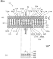
- FIG. 3A is a diagram illustrating the acoustic wave device 10 according to the first embodiment, where (a) is a plan view and (b) is a cross-sectional view taken along the line AA.
- FIG. 3B is a partially enlarged view of the acoustic wave device 10.
- the acoustic wave element 10 is provided on the piezoelectric substrate 100, the IDT electrode 21 provided on the piezoelectric substrate 100, the piezoelectric substrate 100, and adjacent to the IDT electrode 21 and the acoustic wave propagation direction WT.
- Reflectors 32L and 32R arranged together are provided.
- the piezoelectric substrate 100 is made of, for example, a LiTaO 3 piezoelectric single crystal, a LiNbO 3 piezoelectric single crystal, or a piezoelectric ceramic having a predetermined cut angle.
- the IDT electrode 21 is composed of a pair of first comb-shaped electrodes 21a and second comb-shaped electrodes 21b facing each other.
- the first comb electrode 21a has a first cross electrode finger 212
- the second comb electrode 21b has a second cross electrode finger 212b.
- the first cross electrode finger 212a and the second cross electrode finger 212b cross each other when viewed from the elastic wave propagation direction WT.
- the IDT electrode 21 has a laminated structure of an adhesion layer 111 and a main electrode layer 112 as shown in FIG. 3A (b). Similarly to the IDT electrode 21, the reflectors 32 ⁇ / b> L and 32 ⁇ / b> R have a laminated structure of the adhesion layer 111 and the main electrode layer 112.
- the adhesion layer 111 is a layer for improving the adhesion between the piezoelectric substrate 100 and the main electrode layer 112, and, for example, Ti is used as a material.
- the film thickness of the adhesion layer 111 is, for example, 12 nm.
- the main electrode layer 112 is made of, for example, Al containing 1% Cu.
- the film thickness of the main electrode layer 112 is, for example, 162 nm.
- the protective layer 113 is formed so as to cover the IDT electrode 21.
- the protective layer 113 is a layer for the purpose of protecting the main electrode layer 112 from the external environment, adjusting frequency temperature characteristics, and improving moisture resistance, for example, a film containing silicon dioxide as a main component. .
- the wavelength of the acoustic wave element 10 refers to the first cross electrode finger 212a and the second cross electrode finger 212b that constitute the first comb electrode 21a and the second comb electrode 21b shown in FIG. Is defined by the repetition pitch ⁇ .
- the cross width L of the IDT electrode 21 is an electrode finger length where the first cross electrode finger 212a and the second cross electrode finger 212b overlap when viewed from the elastic wave propagation direction WT.
- the acoustic wave device 10 includes the piezoelectric substrate 100, the IDT electrode 21, and the reflectors 32L and 32R.
- the reflectors 32L and 32R are disposed on both sides of the IDT electrode 21 in the elastic wave propagation direction WT.
- Each of the reflectors 32L and 32R includes a first reflective bus bar electrode 320a, a second reflective bus bar electrode 320b, and a plurality of reflective electrode fingers 321.
- Each of the first reflective bus bar electrode 320a and the second reflective bus bar electrode 320b extends in the elastic wave propagation direction WT and is disposed so as to face each other.
- Each of the plurality of reflective electrode fingers 321 is connected to each of the first reflective bus bar electrode 320a and the second reflective bus bar electrode 320b, and extends in a direction orthogonal to the acoustic wave propagation direction WT (hereinafter referred to as orthogonal direction CD).
- orthogonal direction CD a direction orthogonal to the acoustic wave propagation direction WT.
- the first comb-shaped electrode 21a of the IDT electrode 21 includes a first bus bar electrode 210a extending in the elastic wave propagation direction WT and a plurality of first bus bars connected to the first bus bar electrode 210a and extending in the orthogonal direction CD. It consists of electrode fingers 211a.
- the second comb-shaped electrode 21b of the IDT electrode 21 includes a second bus bar electrode 210b extending in the elastic wave propagation direction WT and a plurality of second bus bars connected to the second bus bar electrode 210b and extending in the orthogonal direction CD. It consists of electrode fingers 211b.
- the first bus bar electrode 210a is disposed so as to be connected to the first reflective bus bar electrode 320a of each of the reflectors 32L and 32R.
- the second bus bar electrode 210b is not connected to the reflectors 32L and 32R.
- the first bus bar electrode 210a is directly connected to the input / output terminal 6a to which a surge voltage is input.
- the first reflective bus bar electrode 320a is connected to the input / output terminal 6a via the first bus bar electrode 210a.
- the energization path length between the input / output terminal 6a and the first electrode finger 211a is different from the energization path length between the input / output terminal 6a and the reflective electrode finger 321.
- the energization path length between the input / output terminal 6a and the reflective electrode finger 321 is longer than the energization path length between the input / output terminal 6a and the first electrode finger 211a (first offset electrode finger 213a described later). Is getting longer.
- the first electrode finger 211a has a first cross electrode finger 212a and a first offset electrode finger 213a. Further, the second electrode finger 211b has a second cross electrode finger 212b and a second offset electrode finger 213b.
- the first cross electrode finger 212a and the second cross electrode finger 212b are arranged so as to cross each other when viewed from the elastic wave propagation direction WT.
- the first offset electrode finger 213a is shorter in length than the first cross electrode finger 212a and is disposed to face the orthogonal direction CD with respect to the second cross electrode finger 212b.
- the second offset electrode finger 213b is shorter in length than the second cross electrode finger 212b and is disposed to face the orthogonal direction CD with respect to the first cross electrode finger 212a.
- First offset electrode fingers 213a are respectively provided on both ends of the first bus bar electrode 210a in the elastic wave propagation direction WT. That is, the first offset electrode finger 213a and the reflective electrode finger 321 are adjacent to each other in the elastic wave propagation direction WT.
- the interval i2 between the reflective electrode finger 321 adjacent in the elastic wave propagation direction WT and the first offset electrode finger 213a is the interval between the first offset electrode finger 213a and the first cross electrode finger 212a adjacent in the elastic wave propagation direction WT. It is smaller than i1 (see (a) of FIG. 3B). For example, the interval i2 is 0.005 ⁇ m smaller than the interval i1. Further, the interval i2 is smaller than the interval i3 between the first offset electrode finger 213a and the second cross electrode finger 212b facing each other in the orthogonal direction CD. For example, the interval i2 is 0.005 ⁇ m smaller than the interval i3.
- connection electrode 411 is formed in the region corresponding to the interval i2, that is, the entire opposing region OA where the adjacent reflective electrode finger 321 and the first offset electrode finger 213a face each other. By this connection electrode 411, the adjacent reflective electrode finger 321 and the first offset electrode finger 213a are electrically connected.
- connection electrode 411 is formed by the same process (for example, lift-off method) as the reflective electrode finger 321 and the first offset electrode finger 213a. That is, the adjacent reflective electrode finger 321 and the first offset electrode finger 213a, and the connection electrode 411 positioned between them are formed as a single body and have the same laminated structure as shown in FIG. 3B (b). ing.
- the reflective electrode finger 321 and the first offset electrode finger are disposed in the opposing area OA where the reflective electrode finger 321 and the first offset electrode finger 213a that are adjacent to each other in the acoustic wave propagation direction WT face each other.
- a connection electrode 411 that electrically connects 213a is formed.
- the adjacent reflective electrode finger 321 and the first offset electrode finger 213a are unlikely to have different potentials, and the occurrence of discharge is suppressed. be able to. Thereby, the pressure
- the acoustic wave filter device 1 includes the acoustic wave element 10 and an input / output terminal (for example, an input / output terminal 6a), and the first bus bar electrode of the acoustic wave element 10 is provided at the input / output terminal. 210a is connected.
- the adjacent reflective electrode fingers 321 and the first The offset electrode finger 213a is unlikely to have a different potential, and the occurrence of discharge can be suppressed.
- voltage resistance of the elastic wave filter apparatus 1 can be improved.
- connection electrode 411 that electrically connects the reflective electrode finger 321 and the first offset electrode finger 213a is described as being provided in the counter area OA, but the first offset electrode finger 213a and the connection electrode are not provided.
- 411 is an integral object, the present embodiment can be described as follows without clearly showing the first offset electrode finger 213a and the connection electrode 411.
- the first bus bar electrode 210a has both end portions E1 in contact with the first reflective bus bar electrodes 320a of the reflectors 32L and 32R, and the first bus bar
- the width w2 of the end portion E1 of the electrode 210a is larger than the width w1 of the center portion C1, and the end portion E1 is connected to the first reflective busbar electrode 320a in the elastic wave propagation direction WT by the second cross electrode finger 212b. It extends to the position where it is placed.
- the end E1 of the wide first bus bar electrode 210a is connected to the first reflective bus bar electrode 320a, the end of the first bus bar electrode 210a can be obtained even when a surge voltage is input. It is difficult for the electric field to concentrate on the portion E1, and the pressure resistance can be improved.
- Elastic wave device according to modification 1] 4 is a plan view of an acoustic wave device 10A according to Modification 1 of Embodiment 1.
- FIG. 1 is a plan view of an acoustic wave device 10A according to Modification 1 of Embodiment 1.
- the first cross electrode fingers 212a are provided on both ends of the first bus bar electrode 210a in the acoustic wave propagation direction WT. That is, the first cross electrode finger 212a and the reflective electrode finger 321 are adjacent to each other in the elastic wave propagation direction WT.
- the reflective electrode finger 321 and the first cross electrode finger 212a are electrically connected to the opposing area OA where the reflective electrode finger 321 and the first cross electrode finger 212a adjacent to each other in the elastic wave propagation direction WT face each other.
- a connection electrode 411 to be connected is formed.
- the distance between the reflective electrode finger 321 adjacent in the elastic wave propagation direction WT and the first cross electrode finger 212a is the same as that of the first offset electrode finger 213a adjacent in the elastic wave propagation direction WT. It is smaller than the interval with the cross electrode finger 212a. Further, the distance between the reflective electrode finger 321 and the first cross electrode finger 212a is smaller than the distance between the first cross electrode finger 212a and the second offset electrode finger 213b facing each other in the orthogonal direction CD.
- FIG. 5 is an enlarged plan view of a part of the acoustic wave device 10B according to the second modification of the first embodiment.
- connection electrode 411 is formed to extend in the orthogonal direction CD from the first bus bar electrode 210a, and the tip 411a of the connection electrode 411 in the orthogonal direction CD is rounded. Specifically, the tip 411a of the connection electrode 411 and the tip of the first cross electrode finger 212a adjacent to the connection electrode 411 are rounded.
- the tip 411a of the connection electrode 411 is rounded, even when an instantaneous high voltage is applied to the acoustic wave device 10B, it is difficult for discharge to occur. Thereby, the pressure
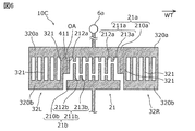
- FIG. 6 is a plan view of an acoustic wave device 10C according to the second embodiment.
- the second offset electrode is arranged in the orthogonal direction CD of the first cross electrode finger 212a electrically connected to the reflective electrode finger 321.
- the finger is not disposed, and the second bus bar electrode 210b is disposed.
- the distance between the first cross electrode finger 212a and the electrode located opposite to the first cross electrode finger 212a is made larger than that of the acoustic wave element 10A of the first modification.
- FIG. 7 is a plan view of an acoustic wave device 10D according to the third embodiment.
- each of the first comb-shaped electrode 21a and the second comb-shaped electrode 21b has offset electrode fingers 213a and 213b. Not done. That is, the first comb-like electrode 21a is configured by the first cross electrode finger 212a and the first bus bar electrode 210a, and the second comb-tooth electrode 21b is configured by the second cross electrode finger 212b and the second bus bar electrode 210b. Has been.
- the first cross electrode finger is not provided with the offset electrode finger in the orthogonal direction CD of the first cross electrode finger 212a. It is possible to suppress the occurrence of discharge in the direction facing 212a. Thereby, the pressure
- FIG. 8 is a plan view of an acoustic wave device 10E according to the fourth embodiment.
- the first bus bar electrode 210a of the first comb-like electrode 21a is replaced with the first reflective bus bar electrode 320a of the reflector 32R. Is connected to only the first reflective bus bar electrode 320a of the reflector 32L.
- the adjacent reflective electrode finger 321 and the first offset electrode finger 213a are unlikely to have different potentials, and the occurrence of discharge is suppressed. be able to. Thereby, the pressure
- the second bus bar electrode 210b is connected to the second reflective bus bar electrode 320b of the reflector 32R, and the opposing area OA of the reflective electrode finger 321 and the second offset electrode finger 213b adjacent to each other in the elastic wave propagation direction WT.
- a connection electrode 411 is formed on the substrate.
- the second bus bar electrode 210b to which the instantaneous high voltage is input is replaced with the first bus bar electrode 210a, and the second offset electrode finger 213b is replaced with the first offset electrode finger 213a. The effect is the same as before.
- the acoustic wave element 10 is not limited to a surface acoustic wave element, and may be a boundary acoustic wave element.
- the materials constituting the adhesion layer 111, the main electrode layer 112, and the protective layer 113 are not limited to the materials described above.
- the IDT electrode 21 does not have to have the above laminated structure.
- the IDT electrode 21 may be made of, for example, a metal or alloy such as Ti, Al, Cu, Pt, Au, Ag, or Pd, or may be made of a plurality of laminates made of the above metal or alloy. May be.
- the protective layer 113 may not be formed.
- the piezoelectric substrate 100 may have a laminated structure in which a high sound velocity supporting substrate, a low sound velocity film, and a piezoelectric film are laminated in this order.
- the piezoelectric film may be, for example, a 50 ° Y-cut X-propagating LiTaO 3 piezoelectric single crystal or a piezoelectric ceramic (a lithium tantalate single crystal cut along a plane whose axis is rotated by 50 ° from the Y axis with the X axis as the central axis, Alternatively, it is made of ceramic and is made of a single crystal or ceramic in which surface acoustic waves propagate in the X-axis direction.
- the piezoelectric film has a thickness of 600 nm, for example.
- the high sound velocity support substrate is a substrate that supports the low sound velocity film, the piezoelectric film, and the IDT electrode.
- the high-sonic support substrate is a substrate in which the acoustic velocity of the bulk wave in the high-sonic support substrate is higher than that of the surface wave or boundary wave that propagates through the piezoelectric film. It functions in such a way that it is confined in the portion where the sonic film is laminated and does not leak below the high sonic support substrate.
- the high sound speed support substrate is, for example, a silicon substrate, and has a thickness of, for example, 200 ⁇ m.
- the low acoustic velocity film is a membrane in which the acoustic velocity of the bulk wave in the low acoustic velocity film is lower than the bulk wave propagating through the piezoelectric membrane, and is disposed between the piezoelectric membrane and the high acoustic velocity support substrate. Due to this structure and the property that energy is concentrated in a medium where acoustic waves are essentially low in sound velocity, leakage of surface acoustic wave energy to the outside of the IDT electrode is suppressed.
- the low acoustic velocity film is, for example, a film mainly composed of silicon dioxide and has a thickness of, for example, 670 nm.
- the Q value at the resonance frequency and the anti-resonance frequency can be greatly increased as compared with a structure in which the piezoelectric substrate 100 is used as a single layer. That is, since a surface acoustic wave resonator having a high Q value can be configured, a filter with a small insertion loss can be configured using the surface acoustic wave resonator.
- the present invention can be widely used in mobile communication devices such as mobile phones as high-frequency filters, duplexers, and multiplexers that can withstand the application of high voltages such as surge voltages.
Landscapes
- Physics & Mathematics (AREA)
- Acoustics & Sound (AREA)
- Surface Acoustic Wave Elements And Circuit Networks Thereof (AREA)
Abstract
Description
本実施の形態に係る弾性波素子は、IDT(Inter Digital Transducer)電極と反射器とを備える。この弾性波素子は、例えば、携帯電話などの移動体通信機のフィルタ(バンドパスフィルタ、ローパスフィルタ、ハイパスフィルタ、バンドエリミネーションフィルタ)として用いられる。本実施の形態の弾性波素子を説明する前に、弾性波素子の課題について図面を参照しつつ説明する。
図1は、比較例に係る弾性波素子510の平面図である。
以下、本発明の実施の形態について、図面を用いて詳細に説明する。なお、以下で説明する実施の形態およびその変形例は、いずれも包括的または具体的な例を示すものである。以下の実施の形態およびその変形例で示される数値、形状、材料、構成要素、構成要素の配置および接続形態などは、一例であり、本発明を限定する主旨ではない。以下の実施の形態およびその変形例における構成要素のうち、独立請求項に記載されていない構成要素については、任意の構成要素として説明される。また、図面に示される構成要素の大きさ、または大きさの比は、必ずしも厳密ではない。
図3Aは、実施の形態1に係る弾性波素子10を表す図であって、(a)は平面図、(b)はA-A線断面図である。図3Bは、弾性波素子10の一部拡大図である。
本実施の形態に係る弾性波素子10では、弾性波伝搬方向WTに隣り合う反射電極指321と第1オフセット電極指213aとが対向する対向領域OAに、反射電極指321と第1オフセット電極指213aとを電気的に接続する接続電極411が形成されている。
図4は、実施の形態1の変形例1に係る弾性波素子10Aの平面図である。
図5は、実施の形態1の変形例2に係る弾性波素子10Bの一部を拡大した平面図である。
図6は、実施の形態2に係る弾性波素子10Cの平面図である。
図7は、実施の形態3に係る弾性波素子10Dの平面図である。
図8は、実施の形態4に係る弾性波素子10Eの平面図である。
以上、本発明の実施の形態およびその変形例に係る弾性波素子および弾性波フィルタ装置ついて説明したが、本発明は、上記実施の形態およびその変形例には限定されない。例えば、上記実施の形態およびその変形例に次のような変形を施した態様も、本発明に含まれる。
2a、2b、2c、2d 直列共振子
3a、3b、3c 並列共振子
4 直列共振子
5 縦結合型弾性波フィルタ部
6a、6b、6c 入出力端子
7 送信フィルタ
8 受信フィルタ
10、10A、10B、10C、10D、10E 弾性波素子
21 IDT電極
21a 第1櫛歯状電極
21b 第2櫛歯状電極
32L、32R 反射器
100 圧電基板
111 密着層
112 主電極層
113 保護層
210a 第1バスバー電極
210b 第2バスバー電極
211a 第1電極指
211b 第2電極指
212a 第1交差電極指
212b 第2交差電極指
213a 第1オフセット電極指
213b 第2オフセット電極指
320a 第1の反射バスバー電極
320b 第2の反射バスバー電極
321 反射電極指
411 接続電極
i1 第1交差電極指と第1オフセット電極指との間隔
i2 反射電極指と第1オフセット電極指との間隔
i3 第1オフセット電極指と第2交差電極指との間隔
OA 対向領域
WT 弾性波伝搬方向
w1 第1バスバー電極の中央部の幅
w2 第1バスバー電極の端部の幅
Claims (12)
- 圧電基板と、
前記圧電基板上に設けられ、互いに対向する第1櫛歯状電極および第2櫛歯状電極を有するIDT電極と、
前記圧電基板上に設けられ、前記IDT電極と弾性波伝搬方向に隣り合って配置された反射器と
を備える弾性波素子であって、
前記反射器は、前記弾性波伝搬方向に延び、互いに対向するように配置された第1の反射バスバー電極および第2の反射バスバー電極と、前記第1の反射バスバー電極および前記第2の反射バスバー電極のそれぞれに接続され、前記弾性波伝搬方向の直交方向に延びるように配置された複数の反射電極指とで構成され、
前記第1櫛歯状電極は、前記弾性波伝搬方向に延び、前記第1の反射バスバー電極に接続されて配置された第1バスバー電極と、前記第1バスバー電極に接続されて前記直交方向に延びるように配置された複数の第1電極指とで構成され、
前記第2櫛歯状電極は、前記弾性波伝搬方向に延び、前記第2の反射バスバー電極に接続されずに配置された第2バスバー電極と、前記第2バスバー電極に接続されて前記直交方向に延びるように配置された複数の第2電極指とで構成され、
前記弾性波伝搬方向に隣り合う前記反射電極指と前記第1電極指とが対向する対向領域に、前記反射電極指と前記第1電極指とを電気的に接続する接続電極が形成されている
弾性波素子。 - 前記対向領域の全ての領域に、前記接続電極が形成されている
請求項1に記載の弾性波素子。 - 前記第1電極指および前記第2電極指は、前記弾性波伝搬方向から見て互いに交差する第1交差電極指および第2交差電極指をそれぞれ有し、
前記第1電極指は、前記第2交差電極指に前記直交方向に対向して配置された第1オフセット電極指を有し、
前記第2電極指は、前記第1交差電極指に前記直交方向に対向して配置された第2オフセット電極指を有し、
前記反射電極指と前記第1オフセット電極指との間に前記接続電極が形成されている
請求項1または2に記載の弾性波素子。 - 前記弾性波伝搬方向に隣り合う前記反射電極指と前記第1オフセット電極指との間隔は、前記弾性波伝搬方向に互いに隣り合う前記第1オフセット電極指と前記第1交差電極指との間隔よりも小さい
請求項3に記載の弾性波素子。 - 前記第1電極指および前記第2電極指は、前記弾性波伝搬方向から見て互いに交差する第1交差電極指および第2交差電極指をそれぞれ有し、
前記第1電極指は、前記第2交差電極指に前記直交方向に対向して配置された第1オフセット電極指を有し、
前記第2電極指は、前記第1交差電極指に前記直交方向に対向して配置された第2オフセット電極指を有し、
前記反射電極指と前記第1交差電極指との間に前記接続電極が形成されている
請求項1または2に記載の弾性波素子。 - 前記弾性波伝搬方向に隣り合う前記反射電極指と前記第1交差電極指との間隔は、前記弾性波伝搬方向に互いに隣り合う前記第1オフセット電極指と前記第1交差電極指との間隔よりも小さい
請求項5に記載の弾性波素子。 - 前記反射電極指に電気的に接続された前記第1交差電極指の前記直交方向には、前記第2オフセット電極指が配置されておらず、前記第2バスバー電極が配置されている
請求項5または6に記載の弾性波素子。 - 前記反射電極指、前記第1電極指および前記接続電極は、同じ層構造を有している
請求項1~7のいずれか1項に記載の弾性波素子。 - 前記接続電極は、前記第1バスバー電極から前記直交方向に延びて形成され、前記直交方向の先端が丸みを帯びている
請求項8に記載の弾性波素子。 - 前記第1バスバー電極には、サージ電圧が入力される
請求項1~9のいずれか1項に記載の弾性波素子。 - 請求項1~10のいずれか1項に記載の弾性波素子と入出力端子とを備える弾性波フィルタ装置であって、
前記入出力端子には、前記弾性波素子の前記第1バスバー電極が接続されている
弾性波フィルタ装置。 - 前記入出力端子および前記第1電極指の間の通電経路長と、前記入出力端子および前記反射電極指の間の通電経路長とが異なる
請求項11に記載の弾性波フィルタ装置。
Priority Applications (4)
| Application Number | Priority Date | Filing Date | Title |
|---|---|---|---|
| KR1020187036200A KR102001429B1 (ko) | 2016-06-24 | 2017-04-25 | 탄성파 소자 및 탄성파 필터장치 |
| CN201780038442.7A CN109417370B (zh) | 2016-06-24 | 2017-04-25 | 弹性波元件及弹性波滤波器装置 |
| JP2018523555A JP6477973B2 (ja) | 2016-06-24 | 2017-04-25 | 弾性波素子および弾性波フィルタ装置 |
| US16/229,076 US10476473B2 (en) | 2016-06-24 | 2018-12-21 | Elastic wave element and elastic wave filter device |
Applications Claiming Priority (2)
| Application Number | Priority Date | Filing Date | Title |
|---|---|---|---|
| JP2016125626 | 2016-06-24 | ||
| JP2016-125626 | 2016-06-24 |
Related Child Applications (1)
| Application Number | Title | Priority Date | Filing Date |
|---|---|---|---|
| US16/229,076 Continuation US10476473B2 (en) | 2016-06-24 | 2018-12-21 | Elastic wave element and elastic wave filter device |
Publications (1)
| Publication Number | Publication Date |
|---|---|
| WO2017221545A1 true WO2017221545A1 (ja) | 2017-12-28 |
Family
ID=60784509
Family Applications (1)
| Application Number | Title | Priority Date | Filing Date |
|---|---|---|---|
| PCT/JP2017/016433 Ceased WO2017221545A1 (ja) | 2016-06-24 | 2017-04-25 | 弾性波素子および弾性波フィルタ装置 |
Country Status (5)
| Country | Link |
|---|---|
| US (1) | US10476473B2 (ja) |
| JP (1) | JP6477973B2 (ja) |
| KR (1) | KR102001429B1 (ja) |
| CN (1) | CN109417370B (ja) |
| WO (1) | WO2017221545A1 (ja) |
Cited By (2)
| Publication number | Priority date | Publication date | Assignee | Title |
|---|---|---|---|---|
| WO2022070885A1 (ja) * | 2020-09-29 | 2022-04-07 | 株式会社村田製作所 | 縦結合共振子型弾性波フィルタ及び弾性波フィルタ |
| WO2023100670A1 (ja) * | 2021-12-01 | 2023-06-08 | 株式会社村田製作所 | フィルタ装置 |
Families Citing this family (2)
| Publication number | Priority date | Publication date | Assignee | Title |
|---|---|---|---|---|
| WO2022075070A1 (ja) * | 2020-10-08 | 2022-04-14 | 株式会社村田製作所 | 縦結合共振子型弾性波フィルタ |
| JP2024135066A (ja) * | 2023-03-22 | 2024-10-04 | 太陽誘電株式会社 | 弾性波デバイス、フィルタ、およびマルチプレクサ |
Citations (2)
| Publication number | Priority date | Publication date | Assignee | Title |
|---|---|---|---|---|
| JP2012065272A (ja) * | 2010-09-17 | 2012-03-29 | Nippon Dempa Kogyo Co Ltd | 弾性波デバイス |
| JP2014143675A (ja) * | 2012-04-25 | 2014-08-07 | Kyocera Corp | 弾性波素子、分波器および通信モジュール |
Family Cites Families (11)
| Publication number | Priority date | Publication date | Assignee | Title |
|---|---|---|---|---|
| JPH07303023A (ja) | 1994-05-07 | 1995-11-14 | Toko Inc | 表面弾性波共振器 |
| JP2004015737A (ja) * | 2002-06-11 | 2004-01-15 | Mitsubishi Electric Corp | 弾性波装置 |
| JP4100249B2 (ja) * | 2003-05-19 | 2008-06-11 | 株式会社村田製作所 | 弾性表面波装置、通信機 |
| JP4480490B2 (ja) * | 2003-07-02 | 2010-06-16 | 京セラ株式会社 | 弾性表面波装置およびそれを用いた通信装置 |
| JP4637600B2 (ja) * | 2005-02-07 | 2011-02-23 | 京セラ株式会社 | 弾性表面波素子および通信装置 |
| JP2007166461A (ja) * | 2005-12-16 | 2007-06-28 | Epson Toyocom Corp | 弾性表面波素子、及びこれを用いた弾性表面波デバイス |
| JP4465625B2 (ja) * | 2006-09-29 | 2010-05-19 | Tdk株式会社 | 弾性表面波フィルタおよび弾性表面波共振器 |
| WO2008126614A1 (ja) * | 2007-03-27 | 2008-10-23 | Murata Manufacturing Co., Ltd. | 弾性波素子 |
| JP5141766B2 (ja) * | 2008-07-10 | 2013-02-13 | 株式会社村田製作所 | 弾性波装置及びラダー型フィルタ装置 |
| JP6585621B2 (ja) * | 2014-12-02 | 2019-10-02 | 京セラ株式会社 | 弾性波素子、分波器および通信モジュール |
| JP6465047B2 (ja) * | 2016-02-19 | 2019-02-06 | 株式会社村田製作所 | 弾性波共振子、帯域通過型フィルタ及びデュプレクサ |
-
2017
- 2017-04-25 KR KR1020187036200A patent/KR102001429B1/ko active Active
- 2017-04-25 WO PCT/JP2017/016433 patent/WO2017221545A1/ja not_active Ceased
- 2017-04-25 CN CN201780038442.7A patent/CN109417370B/zh active Active
- 2017-04-25 JP JP2018523555A patent/JP6477973B2/ja active Active
-
2018
- 2018-12-21 US US16/229,076 patent/US10476473B2/en active Active
Patent Citations (2)
| Publication number | Priority date | Publication date | Assignee | Title |
|---|---|---|---|---|
| JP2012065272A (ja) * | 2010-09-17 | 2012-03-29 | Nippon Dempa Kogyo Co Ltd | 弾性波デバイス |
| JP2014143675A (ja) * | 2012-04-25 | 2014-08-07 | Kyocera Corp | 弾性波素子、分波器および通信モジュール |
Cited By (3)
| Publication number | Priority date | Publication date | Assignee | Title |
|---|---|---|---|---|
| WO2022070885A1 (ja) * | 2020-09-29 | 2022-04-07 | 株式会社村田製作所 | 縦結合共振子型弾性波フィルタ及び弾性波フィルタ |
| US12574014B2 (en) | 2020-09-29 | 2026-03-10 | Murata Manufacturing Co., Ltd. | Longitudinally coupled resonator acoustic wave filter and acoustic wave filter |
| WO2023100670A1 (ja) * | 2021-12-01 | 2023-06-08 | 株式会社村田製作所 | フィルタ装置 |
Also Published As
| Publication number | Publication date |
|---|---|
| US20190131955A1 (en) | 2019-05-02 |
| CN109417370B (zh) | 2020-04-03 |
| JPWO2017221545A1 (ja) | 2019-01-17 |
| KR20180137578A (ko) | 2018-12-27 |
| KR102001429B1 (ko) | 2019-07-18 |
| JP6477973B2 (ja) | 2019-03-06 |
| US10476473B2 (en) | 2019-11-12 |
| CN109417370A (zh) | 2019-03-01 |
Similar Documents
| Publication | Publication Date | Title |
|---|---|---|
| US11496116B2 (en) | Acoustic wave filter device, multiplexer and composite filter device | |
| JP6465065B2 (ja) | 弾性波装置 | |
| US10461718B2 (en) | Acoustic wave resonator, filter, and multiplexer | |
| JP6801797B2 (ja) | 弾性波フィルタ | |
| JP6760480B2 (ja) | エクストラクタ | |
| WO2016017730A1 (ja) | 弾性波素子、フィルタ素子および通信装置 | |
| CN105745840A (zh) | 弹性波元件、分波器以及通信装置 | |
| US11863155B2 (en) | Surface acoustic wave element | |
| WO2018092511A1 (ja) | 弾性表面波フィルタおよびマルチプレクサ | |
| JP6624337B2 (ja) | 弾性波装置、マルチプレクサ、高周波フロントエンド回路及び通信装置 | |
| US10476473B2 (en) | Elastic wave element and elastic wave filter device | |
| JP2017225109A (ja) | マルチプレクサおよび高周波フロントエンドモジュール | |
| KR101711756B1 (ko) | 탄성파 디바이스, 필터 및 분파기 | |
| CN111164891B (zh) | 多工器、高频前端电路以及通信装置 | |
| WO2018117060A1 (ja) | 弾性波共振器、フィルタ装置およびマルチプレクサ | |
| WO2019065861A1 (ja) | マルチプレクサ、高周波フロントエンド回路及び通信装置 | |
| WO2022091582A1 (ja) | 弾性波フィルタ | |
| WO2018117059A1 (ja) | 弾性波共振器、フィルタ装置およびマルチプレクサ | |
| CN117674765A (zh) | 弹性波滤波器及多工器 | |
| WO2023037925A1 (ja) | 弾性波フィルタおよびマルチプレクサ | |
| WO2023074373A1 (ja) | 弾性波共振子、弾性波フィルタ装置およびマルチプレクサ | |
| JP7132841B2 (ja) | 弾性表面波素子、分波器および通信装置 | |
| CN111183584B (zh) | 多工器、高频前端电路以及通信装置 | |
| US11863161B2 (en) | Acoustic wave filter | |
| WO2023282330A1 (ja) | 弾性波素子、弾性波フィルタ装置およびマルチプレクサ |
Legal Events
| Date | Code | Title | Description |
|---|---|---|---|
| ENP | Entry into the national phase |
Ref document number: 2018523555 Country of ref document: JP Kind code of ref document: A |
|
| 121 | Ep: the epo has been informed by wipo that ep was designated in this application |
Ref document number: 17815016 Country of ref document: EP Kind code of ref document: A1 |
|
| ENP | Entry into the national phase |
Ref document number: 20187036200 Country of ref document: KR Kind code of ref document: A |
|
| NENP | Non-entry into the national phase |
Ref country code: DE |
|
| 122 | Ep: pct application non-entry in european phase |
Ref document number: 17815016 Country of ref document: EP Kind code of ref document: A1 |