WO2017221518A1 - 弾性波装置及びその製造方法 - Google Patents
弾性波装置及びその製造方法 Download PDFInfo
- Publication number
- WO2017221518A1 WO2017221518A1 PCT/JP2017/014760 JP2017014760W WO2017221518A1 WO 2017221518 A1 WO2017221518 A1 WO 2017221518A1 JP 2017014760 W JP2017014760 W JP 2017014760W WO 2017221518 A1 WO2017221518 A1 WO 2017221518A1
- Authority
- WO
- WIPO (PCT)
- Prior art keywords
- cover member
- opening edge
- acoustic wave
- elastic wave
- wave device
- Prior art date
- Legal status (The legal status is an assumption and is not a legal conclusion. Google has not performed a legal analysis and makes no representation as to the accuracy of the status listed.)
- Ceased
Links
Images





Classifications
-
- H—ELECTRICITY
- H03—ELECTRONIC CIRCUITRY
- H03H—IMPEDANCE NETWORKS, e.g. RESONANT CIRCUITS; RESONATORS
- H03H3/00—Apparatus or processes specially adapted for the manufacture of impedance networks, resonating circuits, resonators
- H03H3/007—Apparatus or processes specially adapted for the manufacture of impedance networks, resonating circuits, resonators for the manufacture of electromechanical resonators or networks
- H03H3/08—Apparatus or processes specially adapted for the manufacture of impedance networks, resonating circuits, resonators for the manufacture of electromechanical resonators or networks for the manufacture of resonators or networks using surface acoustic waves
-
- H—ELECTRICITY
- H03—ELECTRONIC CIRCUITRY
- H03H—IMPEDANCE NETWORKS, e.g. RESONANT CIRCUITS; RESONATORS
- H03H9/00—Networks comprising electromechanical or electro-acoustic elements; Electromechanical resonators
- H03H9/0023—Networks for transforming balanced signals into unbalanced signals and vice versa, e.g. baluns, or networks having balanced input and output
- H03H9/0028—Networks for transforming balanced signals into unbalanced signals and vice versa, e.g. baluns, or networks having balanced input and output using surface acoustic wave devices
- H03H9/0085—Networks for transforming balanced signals into unbalanced signals and vice versa, e.g. baluns, or networks having balanced input and output using surface acoustic wave devices having four acoustic tracks
-
- H—ELECTRICITY
- H03—ELECTRONIC CIRCUITRY
- H03H—IMPEDANCE NETWORKS, e.g. RESONANT CIRCUITS; RESONATORS
- H03H9/00—Networks comprising electromechanical or electro-acoustic elements; Electromechanical resonators
- H03H9/02—Details
- H03H9/02535—Details of surface acoustic wave devices
- H03H9/02543—Characteristics of substrate, e.g. cutting angles
- H03H9/02574—Characteristics of substrate, e.g. cutting angles of combined substrates, multilayered substrates, piezoelectrical layers on not-piezoelectrical substrate
-
- H—ELECTRICITY
- H03—ELECTRONIC CIRCUITRY
- H03H—IMPEDANCE NETWORKS, e.g. RESONANT CIRCUITS; RESONATORS
- H03H9/00—Networks comprising electromechanical or electro-acoustic elements; Electromechanical resonators
- H03H9/02—Details
- H03H9/02535—Details of surface acoustic wave devices
- H03H9/02992—Details of bus bars, contact pads or other electrical connections for finger electrodes
-
- H—ELECTRICITY
- H03—ELECTRONIC CIRCUITRY
- H03H—IMPEDANCE NETWORKS, e.g. RESONANT CIRCUITS; RESONATORS
- H03H9/00—Networks comprising electromechanical or electro-acoustic elements; Electromechanical resonators
- H03H9/02—Details
- H03H9/05—Holders or supports
- H03H9/10—Mounting in enclosures
- H03H9/1064—Mounting in enclosures for surface acoustic wave [SAW] devices
- H03H9/1092—Mounting in enclosures for surface acoustic wave [SAW] devices the enclosure being defined by a cover cap mounted on an element forming part of the surface acoustic wave [SAW] device on the side of the IDT's
-
- H—ELECTRICITY
- H03—ELECTRONIC CIRCUITRY
- H03H—IMPEDANCE NETWORKS, e.g. RESONANT CIRCUITS; RESONATORS
- H03H9/00—Networks comprising electromechanical or electro-acoustic elements; Electromechanical resonators
- H03H9/02—Details
- H03H9/125—Driving means, e.g. electrodes, coils
- H03H9/145—Driving means, e.g. electrodes, coils for networks using surface acoustic waves
- H03H9/14544—Transducers of particular shape or position
- H03H9/14588—Horizontally-split transducers
-
- H—ELECTRICITY
- H03—ELECTRONIC CIRCUITRY
- H03H—IMPEDANCE NETWORKS, e.g. RESONANT CIRCUITS; RESONATORS
- H03H9/00—Networks comprising electromechanical or electro-acoustic elements; Electromechanical resonators
- H03H9/25—Constructional features of resonators using surface acoustic waves
-
- H—ELECTRICITY
- H03—ELECTRONIC CIRCUITRY
- H03H—IMPEDANCE NETWORKS, e.g. RESONANT CIRCUITS; RESONATORS
- H03H9/00—Networks comprising electromechanical or electro-acoustic elements; Electromechanical resonators
- H03H9/46—Filters
- H03H9/64—Filters using surface acoustic waves
- H03H9/6423—Means for obtaining a particular transfer characteristic
- H03H9/6433—Coupled resonator filters
- H03H9/6483—Ladder SAW filters
-
- H—ELECTRICITY
- H10—SEMICONDUCTOR DEVICES; ELECTRIC SOLID-STATE DEVICES NOT OTHERWISE PROVIDED FOR
- H10N—ELECTRIC SOLID-STATE DEVICES NOT OTHERWISE PROVIDED FOR
- H10N30/00—Piezoelectric or electrostrictive devices
- H10N30/80—Constructional details
- H10N30/88—Mounts; Supports; Enclosures; Casings
-
- H—ELECTRICITY
- H10—SEMICONDUCTOR DEVICES; ELECTRIC SOLID-STATE DEVICES NOT OTHERWISE PROVIDED FOR
- H10W—GENERIC PACKAGES, INTERCONNECTIONS, CONNECTORS OR OTHER CONSTRUCTIONAL DETAILS OF DEVICES COVERED BY CLASS H10
- H10W76/00—Containers; Fillings or auxiliary members therefor; Seals
- H10W76/10—Containers or parts thereof
Definitions
- the present invention relates to a longitudinally coupled resonator type acoustic wave filter, an acoustic wave device having a three-dimensional wiring portion, and a method of manufacturing the same.
- Patent Document 1 a plurality of IDT electrodes are provided on a piezoelectric substrate in order to form a longitudinally coupled resonator type acoustic wave filter.
- a solid wiring portion is provided on the side of the longitudinally coupled resonator type elastic wave filter.
- the three-dimensional wiring portion includes a lower layer wiring, an insulating layer provided on the lower layer wiring, and an upper layer wiring provided on the insulating layer.
- a cover member having an opening opened downward may be provided on the piezoelectric substrate in order to seal a portion where the IDT electrode is provided.
- the cover member is disposed so that the opening edge portion below the cover member surrounds the longitudinally coupled resonator type acoustic wave filter portion.
- the cover member is provided so as to surround not only the longitudinally coupled resonator type acoustic wave filter but also the three-dimensional wiring portion, the size of the acoustic wave device increases.
- the cover member when the cover member is provided so as to surround the three-dimensional wiring portion, or when the cover member is provided so as not to surround the three-dimensional wiring portion and so as to surround the longitudinally coupled resonator type acoustic wave filter, the cover member Since the distance between the IDT electrode and the IDT electrode becomes short, for example, the top plate of the cover member may be recessed toward the piezoelectric substrate due to the pressure of the molding resin covering the cover member, and the cover member and the IDT electrode may come into contact with each other. It was.
- An object of the present invention is to provide an acoustic wave device that can be reduced in size and that does not easily cause contact between a cover member and an IDT electrode.
- An elastic wave device is provided on an element substrate having piezoelectricity, an IDT electrode that is provided on the element substrate and forms a longitudinally coupled resonator type elastic wave filter, and the element substrate.
- a three-dimensional wiring portion connected to the longitudinally coupled resonator type acoustic wave filter, and a cover member surrounding the longitudinally coupled resonator type acoustic wave filter, wherein the three-dimensional wiring portion is a lower layer wiring And an upper layer wiring, and an insulating layer laminated between the lower layer wiring and the upper layer wiring, and the cover member has a portion located on the three-dimensional wiring part.
- the three-dimensional wiring portion is arranged in a direction orthogonal to the elastic wave propagation direction of the longitudinally coupled resonator type elastic wave filter.
- the cover member has an opening edge located on the three-dimensional wiring portion, the insulating layer from the three-dimensional wiring portion along the elastic wave propagation direction, The cover member extends to the outside of the opening edge of the cover member, and the opening edge of the cover member is located not only on the three-dimensional wiring part but also on the insulating layer. In this case, the step between the upper surface of the three-dimensional wiring portion and the upper surface of the extension portion can be reduced. Therefore, the cover member is unlikely to crack.
- the opening edge of the cover member includes first and second opening edge portions extending in an elastic wave propagation direction
- the insulating layer is located below the first and second opening edge portions over the entire length of the second opening edge portion. In this case, the step between the three-dimensional wiring portion and the other portion is reduced over the entire length of the first and second opening edge portions. Therefore, cracks in the cover member are less likely to occur.
- the opening edge of the cover member connects both ends of the first and second opening edge portions, and third and fourth. It has an open edge.
- the insulating layer is located below the first and second opening edge portions and the third and fourth opening edge portions,
- the insulating layer has a frame shape.
- the first and second opening end edges of the cover member are disposed below the first and second opening end edges over the entire length of the first and second opening end edges. Upper layer wiring is located. In this case, cracks in the cover member are less likely to occur.
- the cover member and the insulating layer are mainly composed of the same insulating material. In this case, even if heat is generated during the formation of the cover member or a thermal shock is applied during use, the cover member is unlikely to crack.
- the cover member and the insulating layer are made of the same insulating material.
- the insulating layer is provided so as to reach the IDT electrode.
- the element substrate is a piezoelectric substrate.
- An elastic wave device manufacturing method is connected to an IDT electrode for forming a longitudinally coupled resonator type acoustic wave filter on an element substrate having piezoelectricity, and to the longitudinally coupled resonator type acoustic wave filter. And a step of bonding a cover member surrounding the longitudinally coupled resonator type acoustic wave filter on the element substrate, wherein the three-dimensional wiring unit includes a lower layer wiring and an upper layer wiring. And an insulating layer laminated between the lower layer wiring and the upper layer wiring, and the cover member is joined to the upper layer wiring of the three-dimensional wiring portion.
- the elastic wave device can be reduced in size, and contact between the cover member and the IDT electrode hardly occurs.
- FIG. 1 is a schematic plan view for explaining an acoustic wave device according to a first embodiment of the present invention.
- FIG. 2 is a cross-sectional view of a portion along the line AA in FIG.
- FIG. 3A to FIG. 3C are front sectional views for explaining the method of manufacturing the acoustic wave device according to the first embodiment.
- 4 (a) to 4 (c) are front sectional views for explaining a method of manufacturing the acoustic wave device according to the first embodiment.
- FIG. 5 is a front sectional view for explaining a manufacturing process of the acoustic wave device according to the first embodiment of the present invention.
- FIG. 6 is a front cross-sectional view for explaining an acoustic wave device according to a second embodiment of the present invention.
- FIG. 1 is a schematic plan view for explaining an acoustic wave device according to a first embodiment of the present invention.
- FIG. 2 is a cross-sectional view of a portion along the line AA
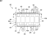
- FIG. 7 is a schematic plan view of an elastic wave device according to a third embodiment of the present invention.
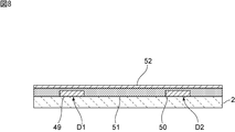
- 8 is a cross-sectional view of the portion along the line CC in FIG. 7 with the cover member and the sealing layer removed.
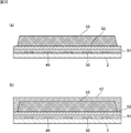
- FIG. 9A to FIG. 9C are front sectional views for explaining a method of manufacturing the acoustic wave device according to the third embodiment.
- FIG. 10A and FIG. 10B are front sectional views for explaining a method of manufacturing the acoustic wave device according to the third embodiment.
- FIG. 11A to FIG. 11C are front sectional views for explaining a method of manufacturing the acoustic wave device according to the third embodiment.
- FIG. 12 is a schematic plan view of an acoustic wave device according to the fourth embodiment of the present invention.
- FIG. 1 is a schematic plan view for explaining an acoustic wave device according to a first embodiment of the present invention.
- a longitudinally coupled resonator type acoustic wave filter 3 and acoustic wave resonators 4 to 7 are formed on a piezoelectric substrate 2 as an element substrate.
- the longitudinally coupled resonator type acoustic wave filter 3 includes three IDT electrodes 8 to 10. In the region where the IDT electrodes 8 to 10 are provided, a reflector 11 is provided on one side in the elastic wave propagation direction, and a reflector 12 is provided on the other side. One end of the IDT electrode 9 is electrically connected to the lower layer wiring 13.
- the upper layer wiring 14 is located above the insulating layer 15 in order to prevent a short circuit with the lower layer wiring 13.
- the lower layer wiring 13, the insulating layer 15, and the upper layer wiring 14 constitute a three-dimensional wiring unit 16.
- a three-dimensional wiring portion 17 is provided on the other side of the IDT electrodes 8 to 10.
- a lower layer wiring 13A, an insulating layer 15A, and an upper layer wiring 14A are laminated.
- the three-dimensional wiring parts 16 and 17 are located outside the longitudinally coupled resonator type elastic wave filter 3 in a direction orthogonal to the elastic wave propagation direction.
- the insulating layers 15 and 15A are made of appropriate insulating ceramics such as SiO 2 or SiN.
- the material of the insulating layers 15 and 15A is not particularly limited as long as the material is mainly an insulating material.
- the IDT electrodes 8 to 10, the reflectors 11 and 12, the lower layer wirings 13 and 13A, and the upper layer wirings 14 and 14A are made of appropriate metals or alloys.
- a laminated metal film in which a plurality of metal films are laminated may be used.
- a cover member 21 is bonded onto the piezoelectric substrate 2.
- cover members 22 to 25 are bonded onto the piezoelectric substrate 2 in order to seal the acoustic wave resonators 4 to 7.
- FIG. 2 is a cross-sectional view taken along the line AA in FIG.
- the cover member 21 has an opening edge that opens downward.
- a cross section of a portion of the IDT electrode 9 where the electrode finger 9a is provided is shown.
- the sealing layer 26 shown in FIG. 2 is provided so as to cover the cover member 21.
- the sealing layer 26 is made of an insulating ceramic such as Al 2 O 3 or SiN, or a synthetic resin such as polyimide or epoxy resin.
- the cover member 21 is provided with etching holes 21a and 21b.
- a sealing layer 26 is provided to seal the etching holes 21a and 21b.
- the etching holes 21a and 21b are provided to remove the sacrificial layer provided in the cover member 21, as is apparent from the description of the manufacturing method described later.
- insulating layers 15 and 15A are laminated between the lower wirings 13 and 13A and the upper wirings 14 and 14A.
- a lower opening edge 21c of the cover member 21 is stacked on the upper layer wirings 14 and 14A. That is, a part of the lower opening edge 21 c of the cover member 21 is located above the three-dimensional wiring parts 16, 17 and is joined to the upper surfaces of the three-dimensional wiring parts 16, 17. Accordingly, the size of the cover member 21 in the portion where the longitudinally coupled resonator type acoustic wave filter 3 is configured can be reduced. As described above, when the cover member is provided so as to surround the three-dimensional wiring portion, the dimension in the direction orthogonal to the elastic wave propagation direction becomes large.
- a part of the lower opening edge 21c of the cover member 21 is located above the three-dimensional wiring parts 16 and 17, and is joined to the upper surfaces of the three-dimensional wiring parts 16 and 17. Therefore, in order to provide a part of the lower opening edge 21c of the cover member 21 between the three-dimensional wiring parts 16 and 17 and the IDT electrode 9, the distance between the three-dimensional wiring parts 16 and 17 and the IDT electrode 9 is increased. There is no need. Therefore, the dimension of the cover member 21 in the direction orthogonal to the elastic wave propagation direction can be effectively reduced, and the elastic wave device 1 can be reduced in size.
- the top plate of the cover member 21 is recessed on the piezoelectric substrate 2 side. Even so, contact between the IDT electrode 9 and the cover member 21 can be suppressed.
- FIGS. 4 (a) to 4 (c) and FIG. 5 the longitudinally coupled resonator type acoustic wave filter 3 of the acoustic wave device 1 is provided. A method for manufacturing the part will be described.
- an IDT electrode 9 having electrode fingers 9a and lower layer wirings 13 and 13A are formed on a piezoelectric substrate 2 as an element substrate.
- a method for forming the IDT electrode 9 and the lower layer wirings 13 and 13A is not particularly limited. For example, a vapor deposition lift-off method can be used.
- insulating layers 15 and 15A are formed on the lower layer wirings 13 and 13A.
- This insulating layer can be formed by sputtering or the like.
- upper wirings 14 and 14A are formed on the insulating layers 15 and 15A.
- the upper wirings 14 and 14A can also be formed using a vapor deposition lift-off method or the like.
- a sacrificial layer Z is provided so as to cover the IDT electrode 9.
- the sacrificial layer Z is provided so as to reach a part on the three-dimensional wiring parts 16 and 17.
- the sacrificial layer Z is provided so as to fill the inside of the cover member 21 described above.
- a material constituting the sacrificial layer Z an appropriate material that can be eluted with an organic solvent or an acid mixed solution can be used.
- polyimide, epoxy resin, or the like can be suitably used.
- an insulating material is applied on the sacrificial layer Z to form the cover member 21.
- the material of the cover member 21 is not particularly limited as long as it is an insulating material, but SiO 2 , SiN, or the like can be used. Also, the method for forming the cover member 21 is not particularly limited, but CVD, sputtering, or the like can be suitably used.
- etching holes 21a and 21b are provided in the top plate of the cover member 21 by an etching method such as dry etching.
- the sacrificial layer Z in the cover member 21 is removed using a liquid that elutes the sacrificial layer Z using the etching holes 21a and 21b.
- a structure in which the inside of the cover member 21 is a hollow space can be obtained.
- the sealing layer 26 is provided so as to cover the outer surface of the cover member 21. In this way, the elastic wave device 1 can be obtained.
- the insulating layers 15 and 15A are made of the same insulating material as the cover member 21. In that case, the type of material can be reduced. Further, even if a thermal shock is applied during the manufacturing process and during actual use, the cover member 21 is more unlikely to crack because the difference in thermal expansion coefficient is small.
- FIG. 6 is a front sectional view of the acoustic wave device according to the second embodiment of the present invention.
- a longitudinally coupled resonator type acoustic wave filter configured in the same manner as in the above embodiment is sealed with a cover member 21 and a sealing layer 26 on a piezoelectric substrate 32 as an element substrate.
- a stopped structure is provided.
- the insulating layer 15B is formed so as to cover not only the three-dimensional wiring part but also the part where the IDT electrode 9 is provided.
- the insulating layer 15B may be provided so as to cover the IDT electrode 9 constituting the longitudinally coupled resonator type acoustic wave filter.
- an IDT electrode 33 constituting an acoustic wave resonator is provided on the side of a region where the IDT electrode 9 constituting the longitudinally coupled resonator type acoustic wave filter is provided. ing.
- the insulating layer 15 ⁇ / b> B described above is extended so as to cover the IDT electrode 33 also in the portion constituting the acoustic wave resonator.
- the cover member 34 is disposed so that the opening edge of the cover member 34 is located on the insulating layer 15B even in the portion where the acoustic wave resonator is formed.
- a sealing layer 35 is provided so as to cover the cover member 34.
- the opening edge of the cover member 34 is bonded onto the insulating layer 15 ⁇ / b> B laminated on the wirings 36 and 37.
- a part of the lower opening edge 21c of the cover member 21 is located above the three-dimensional wiring parts 16 and 17, and is joined to the upper surfaces of the three-dimensional wiring parts 16 and 17. Therefore, in order to provide a part of the lower opening edge 21c of the cover member 21 between the three-dimensional wiring parts 16 and 17 and the IDT electrode 9, the elastic wave propagation direction is also orthogonal to the portion where the elastic wave resonator is provided. It is possible to reduce the dimension in the direction to be performed. Also in the elastic wave device 31, since the opening edge of the cover member 21 is located on the three-dimensional wiring portion as described above, the size can be reduced. In addition, cracks in the cover members 21 and 34 hardly occur.
- FIG. 7 is a schematic plan view of the acoustic wave device according to the third embodiment.
- a cover member 42 is provided so as to surround the 5IDT type longitudinally coupled resonator type acoustic wave filter.
- a sealing layer 43 is provided on the top plate of the cover member 42.
- the acoustic wave device 41 is provided with five IDT electrodes 44 to 48.
- reflectors are provided on both sides of the region where the IDT electrodes 44 to 48 are provided in the elastic wave propagation direction.
- the opening edge of the cover member 42 is substantially rectangular, and the first and second opening edge portions 42a and 42b extending in the elastic wave propagation direction are connected to the first and second opening edge portions 42a and 42b. And have third and fourth opening edge portions 42c and 42d extending in a direction orthogonal to the elastic wave propagation direction.
- an insulating layer is provided so as to reach the entire length of the first opening edge 42a as well as a portion where the three-dimensional wiring portion indicated by arrows D1 and D2 is provided. Yes.
- FIG. 8 is a cross-sectional view in which the cover member 42 and the sealing layer 43 are removed from the portion along the line CC in FIG.
- lower layer wirings 49 and 50 are provided on the piezoelectric substrate 2 as an element substrate.
- the lower layer wirings 49 and 50 are connected to one ends of the IDT electrodes 45 and 47 as shown in FIG.
- An insulating layer 51 is provided so as to cover the lower layer wirings 49 and 50.
- An upper wiring 52 is provided so as to electrically connect one ends of the IDT electrodes 44, 46, and 48. Therefore, in the three-dimensional wiring portion indicated by the arrows D1 and D2, the insulating layer 51 is laminated between the lower layer wiring 49 and the upper layer wiring 52 or between the lower layer wiring 50 and the upper layer wiring 52.
- the first opening edge 42a of the cover member 42 is located above the portion where the upper layer wiring 52 is provided, as shown in FIG. That is, in the elastic wave propagation direction, the insulating layer 51 is located below the first opening edge portion 42a over the entire length of the first opening edge portion 42a. Accordingly, in the insulating layer 51, there is a very large step between the upper surface of the three-dimensional wiring portion indicated by the arrows D1 and D2 and the upper surface of the insulating layer 51 extending to the outside of the first opening edge portion 42a. small. Therefore, the cover member 42 is firmly joined. Therefore, even if heat or the like is applied, the step is small, so that the cover member 42 is hardly cracked.
- the insulating layer 51 is located below the second opening edge 42b over the entire length of the second opening edge 42b. Therefore, in the insulating layer 51, there is a very large step between the upper surface of the three-dimensional wiring portion indicated by the arrows D3 and D4 and the upper surface of the insulating layer 51 extending to the outside of the second opening edge portion 42b. small.
- FIGS. 9A to 9C A method of manufacturing the elastic wave device 41 will be described with reference to FIGS. 9A to 9C, FIGS. 10A and 10B, and FIGS. 11A to 11C. To do.
- a plurality of lower layer wirings including lower layer wirings 49 and 50 are formed on the piezoelectric substrate 2 as an element substrate by a vapor deposition lift-off method or the like.
- the insulating layer 51 is formed by CVD or sputtering.
- the upper surface of the insulating layer 51 is flat, but actually protrudes slightly upward in the portion where the lower layer wirings 49 and 50 are provided.
- the upper layer wiring 52 is formed on the insulating layer 51.
- the formation of the upper wiring 52 is not particularly limited, and an evaporation lift-off method or the like can be used as appropriate.
- a sacrificial layer 53 is provided.
- the sacrificial layer 53 can be made of the same material as the sacrificial layer 22 described above.
- a cover member 42 is provided on the sacrificial layer 53 as shown in FIG.
- the cover member 42 can be formed using CVD, sputtering, or the like.
- etching holes 42e and 42f are provided in the cover member 42.
- the etching holes 42e and 42f can be formed by dry etching or the like.
- the sacrificial layer 53 is removed by an etchant or the like using the etching holes 42e and 42f. Thereby, the hollow space E is formed.
- a sealing layer 43 is provided on the top plate of the cover member 42 so as to seal the etching holes 42e and 42f. In this way, the elastic wave device 41 can be obtained.
- FIG. 12 is a schematic plan view of an acoustic wave device according to the fourth embodiment of the present invention.
- a frame-shaped insulating layer 51A is provided in the acoustic wave device 61.
- the insulating layer 51A is located below the first and second opening edge portions 42a and 42b of the cover member 42 and below the third and fourth opening edge portions 42c and 42d.
- the elastic wave device 61 is the same as the elastic wave device 41. Accordingly, the same parts are denoted by the same reference numerals, and the description thereof is omitted.
- the insulating layer 51A may be provided so as to be positioned below the entire opening edge of the cover member 42. In this case, since the insulating layer 51A is located below the third and fourth opening edge portions 42c and 42d, the bonding strength of the cover member 42 can be further effectively increased.
- the element substrate is configured by a piezoelectric substrate.
- the element substrate having piezoelectricity in the present invention may be formed by laminating a piezoelectric thin film on a support substrate or an acoustic multilayer film.
- elastic wave device 42 cover member 42a ... first opening edge 42b ... second opening end Edge 42c ... third opening edge 42d ... fourth opening edge 42e, 42f ... etching hole 43 ... sealing layers 44-48 ... IDT electrodes 49, 50 ... lower wirings 51, 51A ... insulating layer 52 ... upper layer wiring 53 ... sacrifice Layer 61 ... acoustic wave device Z ... sacrificial layer
Landscapes
- Physics & Mathematics (AREA)
- Acoustics & Sound (AREA)
- Engineering & Computer Science (AREA)
- Manufacturing & Machinery (AREA)
- Surface Acoustic Wave Elements And Circuit Networks Thereof (AREA)
- Piezo-Electric Or Mechanical Vibrators, Or Delay Or Filter Circuits (AREA)
Abstract
小型化を図ることができ、かつ、カバー部材とIDT電極との接触が生じ難い、弾性波装置を提供する。 素子基板としての圧電基板2上に、縦結合共振子型弾性波フィルタ3を構成しているIDT電極9が設けられており、圧電基板2上に、縦結合共振子型弾性波フィルタ3に接続されている立体配線部16が設けられており、圧電基板2上に、縦結合共振子型弾性波フィルタ3を囲むカバー部材21とを備える、弾性波装置1。立体配線部16が、下層配線13と上層配線14と、下層配線13及び上層配線14間に積層されている絶縁層15とを有し、カバー部材21が、立体配線部16上に位置している部分を有する。
Description
本発明は、縦結合共振子型弾性波フィルタ及び立体配線部を有する弾性波装置及びその製造方法に関する。
従来、縦結合共振子型弾性波フィルタを有する弾性波装置が種々提案されている。下記の特許文献1では、圧電基板上に、縦結合共振子型弾性波フィルタを構成するために、複数のIDT電極が設けられている。縦結合共振子型弾性波フィルタの側方には、立体配線部が設けられている。立体配線部は、下層配線と、下層配線上に設けられた絶縁層と、絶縁層上に設けられた上層配線とを有する。
弾性波装置では、IDT電極が設けられている部分を封止するために、圧電基板上に下方に開いた開口を有するカバー部材を設けることがある。この場合、カバー部材の下方の開口端縁部が、縦結合共振子型弾性波フィルタ部分を囲むように、カバー部材が配置される。ところが、上記縦結合共振子型弾性波フィルタだけでなく、立体配線部をも囲むようにカバー部材を設けると、弾性波装置の寸法が大きくなる。
他方、立体配線部を囲まないように、かつ、縦結合共振子型弾性波フィルタを囲むようにカバー部材を設けた場合には、IDT電極と立体配線部との間にカバー部材の開口端縁が位置する。そのため、縦結合共振子型弾性波フィルタを構成しているIDT電極と、立体配線部との間のスペースを大きくする必要がある。従って、弾性波装置の寸法が大きくなるという問題があった。
また、立体配線部を囲むようにカバー部材を設ける場合や、立体配線部を囲まないように、かつ、縦結合共振子型弾性波フィルタを囲むようにカバー部材を設けた場合には、カバー部材とIDT電極との距離が近くなってしまうので、例えば、カバー部材を覆うモールド樹脂の圧力等により、カバー部材の天板が圧電基板側に凹み、カバー部材とIDT電極とが接触するおそれがあった。
本発明の目的は、小型化を図ることができ、かつ、カバー部材とIDT電極との接触が生じ難い、弾性波装置を提供することにある。
本発明に係る弾性波装置は、圧電性を有する素子基板と、前記素子基板上に設けられており、縦結合共振子型弾性波フィルタを構成しているIDT電極と、前記素子基板上に設けられており、前記縦結合共振子型弾性波フィルタに接続されている、立体配線部と、前記縦結合共振子型弾性波フィルタを囲むカバー部材と、を備え、前記立体配線部が、下層配線と、上層配線と、前記下層配線と前記上層配線との間に積層されている絶縁層と、を有し、前記カバー部材が、前記立体配線部上に位置している部分を有する。
本発明に係る弾性波装置のある特定の局面では、前記立体配線部が、前記縦結合共振子型弾性波フィルタの弾性波伝搬方向と直交する方向において、前記縦結合共振子型弾性波フィルタの外側に設けられており、前記カバー部材は、前記立体配線部上に位置している開口端縁を有しており、前記絶縁層が、前記立体配線部から、弾性波伝搬方向に沿って、前記カバー部材の前記開口端縁の外まで延ばされており、前記カバー部材の前記開口端縁が、前記立体配線部上だけでなく、前記絶縁層上にも位置している。この場合には、立体配線部の上面と、延長部の上面との段差を小さくすることができる。従って、カバー部材のクラックが生じ難い。
本発明に係る弾性波装置のさらに他の特定の局面では、前記カバー部材の前記開口端縁が、弾性波伝搬方向に延びる第1,第2の開口端縁部を有し、前記第1,第2の開口端縁部の全長にわたり、前記第1,第2の開口端縁部の下方に前記絶縁層が位置している。この場合には、第1,第2の開口端縁部の全長にわたり、立体配線部と他の部分との間の段差が小さくなる。従って、カバー部材のクラックがより一層生じ難い。
本発明に係る弾性波装置の別の特定の局面では、前記カバー部材の前記開口端縁が、前記第1,第2の開口端縁部の両端を連結している、第3,第4の開口端縁部を有する。
本発明に係る弾性波装置の他の特定の局面では、前記第1,第2の開口端縁部及び前記第3,第4の開口端縁部の下方に前記絶縁層が位置しており、前記絶縁層が枠状の形状を有している。
本発明に係る弾性波装置のさらに他の特定の局面では、前記カバー部材の前記第1,第2の開口端縁部の全長にわたり、前記第1,第2の開口端縁部の下方に前記上層配線が位置している。この場合には、カバー部材のクラックがより一層生じ難い。
本発明に係る弾性波装置の別の特定の局面では、前記カバー部材及び前記絶縁層が、同一絶縁性材料を主体とする。この場合には、カバー部材の形成に際して熱が生じたとしても、また使用中に熱衝撃が加わったとしても、カバー部材のクラックが生じ難い。
好ましくは、前記カバー部材及び前記絶縁層は同一絶縁性材料からなることが望ましい。
本発明に係る弾性波装置のさらに他の特定の局面では、前記絶縁層が、前記IDT電極上に至るように設けられている。
本発明に係る弾性波装置の別の特定の局面では、前記素子基板が、圧電基板である。
本発明に係る弾性波装置の製造方法は、圧電性を有する素子基板上に、縦結合共振子型弾性波フィルタを構成するためのIDT電極と、前記縦結合共振子型弾性波フィルタに接続されている立体配線部とを設ける工程と、前記素子基板上に、前記縦結合共振子型弾性波フィルタを囲むカバー部材を接合する工程とを備え、前記立体配線部が、下層配線と、上層配線と、前記下層配線と前記上層配線との間に積層されている絶縁層とを有し、前記カバー部材が、前記立体配線部の前記上層配線に接合されている。
本発明に係る弾性波装置及びその製造方法によれば、弾性波装置の小型化を図ることができ、かつ、カバー部材とIDT電極との接触が生じ難い。
以下、図面を参照しつつ、本発明の具体的な実施形態を説明することにより、本発明を明らかにする。
なお、本明細書に記載の各実施形態は、例示的なものであり、異なる実施形態間において、構成の部分的な置換または組み合わせが可能であることを指摘しておく。
図1は、本発明の第1の実施形態に係る弾性波装置を説明するための模式的平面図である。弾性波装置1では、素子基板としての圧電基板2上に縦結合共振子型弾性波フィルタ3、弾性波共振子4~7が構成されている。縦結合共振子型弾性波フィルタ3は、3個のIDT電極8~10を有する。IDT電極8~10が設けられている領域の弾性波伝搬方向一方側に反射器11が、他方側に反射器12が設けられている。IDT電極9の一端が、下層配線13に電気的に接続されている。また、IDT電極8,10の一端同士が、上層配線14により共通接続されている。この上層配線14は、下層配線13との短絡を防止するために、絶縁層15の上方に位置している。それによって、下層配線13と、絶縁層15と、上層配線14とにより、立体配線部16が構成されている。IDT電極8~10の他方側においても、同様に立体配線部17が設けられている。立体配線部17では、下層配線13A、絶縁層15A、上層配線14Aが積層されている。立体配線部16,17は、弾性波伝搬方向と直交する方向において、縦結合共振子型弾性波フィルタ3の外側に位置している。
上記絶縁層15,15Aは、SiO2や、SiNなどの適宜の絶縁性セラミックスからなる。もっとも、絶縁層15,15Aの材料は、絶縁性材料を主体とする限り、特に限定されるものではない。
他方、IDT電極8~10及び反射器11,12、下層配線13,13A、上層配線14,14Aは、適宜の金属もしくは合金からなる。また、複数の金属膜を積層した積層金属膜が用いられてもよい。
上記縦結合共振子型弾性波フィルタ3を封止するために、カバー部材21が圧電基板2上に接合されている。なお、弾性波共振子4~7を封止するために、同様にカバー部材22~25が圧電基板2上に接合されている。
図2は、図1のA-A線に沿う部分の断面図である。カバー部材21は、下方に開いた開口端縁を有する。IDT電極9の電極指9aが設けられている部分の断面が示されている。図1では図示を省略しているが、カバー部材21を覆うように図2に示す封止層26が設けられている。封止層26は、Al2O3、SiNなどの絶縁性セラミックス、またはポリイミドやエポキシ樹脂などの合成樹脂からなる。
図2に示すように、カバー部材21には、エッチング用孔21a,21bが設けられている。このエッチング用孔21a,21bを封止するために封止層26が設けられている。エッチング用孔21a,21bは、後述する製造方法の説明から明らかなように、カバー部材21内に設けられた犠牲層を除去するために設けられている。
図2に示すように、立体配線部16,17においては、下方配線13,13Aと、上層配線14,14Aとの間に、絶縁層15,15Aが積層されている。カバー部材21の下方開口端縁21cが、上層配線14,14A上に積層されている。すなわち、カバー部材21の下方開口端縁21cの一部が、立体配線部16,17の上方に位置しており、立体配線部16,17の上面に接合されている。従って、縦結合共振子型弾性波フィルタ3が構成されている部分におけるカバー部材21の寸法を小さくすることができる。前述したように、立体配線部をも囲むように上記カバー部材を設けた場合、弾性波伝搬方向と直交する方向の寸法が大きくなる。
また、本実施形態では、カバー部材21の下方開口端縁21cの一部が、立体配線部16,17の上方に位置しており、立体配線部16,17の上面に接合されている。そのため、カバー部材21の下方開口端縁21cの一部を立体配線部16,17とIDT電極9との間に設けるために立体配線部16,17とIDT電極9との間の距離を大きくする必要もない。従って、カバー部材21の弾性波伝搬方向と直交する方向の寸法を効果的に小さくすることができ、弾性波装置1の小型化を図ることができる。さらに、立体配線部16,17の上にカバー部材21を設けることで、カバー部材21とIDT電極9との距離が離れるため、カバー部材21の天板が圧電基板2側に凹んだ場合であったとしても、IDT電極9とカバー部材21との接触を抑制することができる。
図3(a)~図3(c)、図4(a)~図4(c)及び図5を参照して、上記弾性波装置1の縦結合共振子型弾性波フィルタ3が設けられている部分の製造方法を説明する。
図3(a)に示すように、素子基板としての圧電基板2上に、電極指9aを有するIDT電極9及び下層配線13,13Aを形成する。このIDT電極9及び下層配線13,13Aの形成方法としては、特に限定されないが、例えば蒸着リフトオフ法を用いることができる。
次に、下層配線13,13A上に図3(b)に示すように、絶縁層15,15Aを形成する。この絶縁層の形成は、スパッタリング等により行い得る。
しかる後、図3(c)に示すように、絶縁層15,15A上に、上層配線14,14Aを形成する。この上層配線14,14Aの形成についても蒸着リフトオフ法などを用いて行い得る。
次に、図4(a)に示すように、犠牲層Zを、IDT電極9を覆うように設ける。この犠牲層Zは、立体配線部16,17上の一部に至るように設ける。また、犠牲層Zは、前述したカバー部材21の内部を充填する形状となるように設けられる。犠牲層Zを構成する材料については、有機溶剤や酸混合溶液により溶出され得る適宜の材料を用いることができる。例えば、ポリイミドやエポキシ樹脂などを好適に用いることができる。
図4(b)に示すように、上記犠牲層Z上に、絶縁性材料を付与し、カバー部材21を形成する。カバー部材21の材料については、絶縁性材料であれば特に限定されないが、SiO2、SiNなどを用いることができる。またカバー部材21の形成方法についても特に限定されないが、CVDやスパッタなどを好適に用いることができる。
次に、図4(c)に示すように、ドライエッチングなどのエッチング法により、エッチング用孔21a,21bを、カバー部材21の天板に設ける。
しかる後、エッチング用孔21a,21bを利用して、犠牲層Zを溶出する液体を用いて、カバー部材21内の犠牲層Zを除去する。このようにして、図5に示すように、カバー部材21内が中空空間とされている構造を得ることができる。最後に、カバー部材21の外表面を被覆するように封止層26を設ける。このようにして、弾性波装置1を得ることができる。
また、好ましくは、上記絶縁層15,15Aが、カバー部材21と同じ絶縁性材料からなることが望ましい。その場合には、材料の種類を低減することができる。また、製造工程において、並びに実使用時に熱衝撃が加わったとしても、熱膨張係数差が小さいため、カバー部材21にクラックが一層生じ難い。
図6は、本発明の第2の実施形態に係る弾性波装置の正面断面図である。第2の実施形態の弾性波装置31では、素子基板としての圧電基板32上に、上記実施形態と同様に構成された縦結合共振子型弾性波フィルタがカバー部材21及び封止層26で封止されている構造が設けられている。但し、絶縁層15Bが、立体配線部だけでなく、IDT電極9が設けられている部分をも覆うように形成されている。このように、縦結合共振子型弾性波フィルタを構成しているIDT電極9をも覆うように絶縁層15Bが設けられていてもよい。
また、弾性波装置31では、縦結合共振子型弾性波フィルタを構成しているIDT電極9が設けられている領域の側方に、弾性波共振子を構成しているIDT電極33が設けられている。この弾性波共振子を構成している部分においても、IDT電極33を覆うように前述した絶縁層15Bが延ばされている。そして、弾性波共振子が構成されている部分においても、カバー部材34の開口端縁が絶縁層15B上に位置するようにカバー部材34が配置されている。カバー部材34を覆うように封止層35が設けられている。図6では、カバー部材34の開口端縁が、配線36,37上に積層されている絶縁層15B上に接合されている。カバー部材21の下方開口端縁21cの一部が、立体配線部16,17の上方に位置しており、立体配線部16,17の上面に接合されている。そのため、カバー部材21の下方開口端縁21cの一部を立体配線部16,17とIDT電極9との間に設けるために弾性波共振子が設けられている部分においても弾性波伝搬方向と直交する方向の寸法を小さくすることができる。弾性波装置31においても、上記のように、立体配線部上に、カバー部材21の開口端縁が位置しているため、小型化を図ることができる。また、カバー部材21,34におけるクラックも生じ難い。
図7は、第3の実施形態に係る弾性波装置の模式的平面図である。弾性波装置41では、5IDT型の縦結合共振子型弾性波フィルタを囲むように、カバー部材42が設けられている。なお、カバー部材42の天板には、封止層43が設けられている。図7に破線で示すように、弾性波装置41では、5個のIDT電極44~48が設けられている。図7では図示を省略しているが、実際には、IDT電極44~48が設けられている領域の弾性波伝搬方向両側には、反射器が設けられている。
縦結合共振子型弾性波フィルタでは、隣り合うIDT電極の同じ側の端部が異なる電位に接続される。従って、弾性波装置41においても、矢印D1~D4で示す部分において立体配線部が設けられることになる。そして、弾性波装置41では、立体配線部における絶縁層が、立体配線部だけでなく、弾性波伝搬方向に沿って延長されている。これをより詳細に説明する。
カバー部材42の開口端縁は略矩形であり、弾性波伝搬方向に延びる第1,第2の開口端縁部42a,42bと、第1,第2の開口端縁部42a,42bを結んでおり、弾性波伝搬方向と直交する方向に延びる第3,第4の開口端縁部42c,42dとを有する。弾性波装置41では、矢印D1,D2で示されている立体配線部が設けられている部分だけでなく、絶縁層が、この第1の開口端縁部42aの全長に至るように設けられている。
図8は、図7のC-C線に沿う部分において、カバー部材42及び封止層43を取り除いた断面図である。
図8に示すように、素子基板としての圧電基板2上に、下層配線49,50が設けられている。下層配線49,50は、図7に示すように、IDT電極45,47の一端に接続されている。下層配線49,50を覆うように、絶縁層51が設けられている。なお、IDT電極44,46,48の一端同士を電気的に接続するように上層配線52が設けられている。従って、矢印D1,D2で示されている立体配線部では、下層配線49と上層配線52との間、あるいは下層配線50と上層配線52との間に、絶縁層51が積層されている。
ところで、上記カバー部材42の第1の開口端縁部42aは、図7に示すように、上層配線52が設けられている部分の上方に位置している。すなわち、弾性波伝搬方向において、第1の開口端縁部42aの全長にわたり、第1の開口端縁部42aの下方に絶縁層51が位置している。従って、絶縁層51において、矢印D1,D2で示す立体配線部部分の上面と、第1の開口端縁部42aの外まで延ばされている絶縁層51の上面との間の段差が非常に小さい。よって、カバー部材42が強固に接合されている。そのため、熱等が加わったとしても、上記段差が小さいため、カバー部材42のクラックが生じ難い。同様に、第2の開口端縁部42bの全長にわたり、第2の開口端縁部42bの下方にも絶縁層51が位置している。従って、絶縁層51において、矢印D3,D4で示す立体配線部部分の上面と、第2の開口端縁部42bの外まで延ばされている絶縁層51の上面との間の段差が非常に小さい。
上記弾性波装置41の製造方法を、図9(a)~図9(c)、図10(a)及び図10(b)並びに図11(a)~図11(c)を参照して説明する。
図9(a)に示すように、素子基板としての圧電基板2上に、蒸着リフトオフ法などにより、下層配線49,50を含む複数の下層配線を形成する。図9(b)に示すように、CVDまたはスパッタリングなどにより、絶縁層51を形成する。図9(b)では、絶縁層51の上面は平坦であるが、実際には、下層配線49,50が設けられている部分において、若干上方に突出する。しかるのち、図9(c)に示すように、絶縁層51上に、上層配線52を形成する。上層配線52の形成についても、蒸着リフトオフ法などを適宜用いることができ、特に限定されない。
次に、図10(a)に示すように、犠牲層53を設ける。犠牲層53は、前述した犠牲層22と同様の材料で構成され得る。犠牲層53上に、図10(b)に示すように、カバー部材42を設ける。カバー部材42の形成は、CVDやスパッタリングなどを用いて行われ得る。
しかる後、図11(a)に示すように、カバー部材42に、エッチング用孔42e,42fを設ける。エッチング用孔42e,42fは、ドライエッチングなどにより形成することができる。次に、図11(b)に示すように、上記エッチング用孔42e,42fを利用して、エッチャントなどにより、犠牲層53を除去する。それによって、中空空間Eが形成される。
次に、図11(c)に示すように、封止層43をエッチング用孔42e,42fを封止するように、カバー部材42の天板上に設ける。このようにして、弾性波装置41を得ることができる。
弾性波装置41の製造に際し、上記封止層43の形成やモールド樹脂の形成に際し熱が加わったとしても、カバー部材42の開口端縁における段差が小さくされているため、カバー部材42のクラックが生じ難い。
図12は、本発明の第4の実施形態に係る弾性波装置の模式的平面図である。弾性波装置61では、枠状の絶縁層51Aが設けられている。絶縁層51Aは、カバー部材42の第1,第2の開口端縁部42a,42bの下方及び第3,第4の開口端縁部42c,42dの下方に位置している。その他の点については、弾性波装置61は、弾性波装置41と同様である。従って、同一部分については、同一の参照番号を付することにより、その説明を省略する。
絶縁層51Aのように、カバー部材42の開口端縁全体の下方に位置するように、絶縁層51Aを設けてもよい。この場合、第3,第4の開口端縁部42c,42dの下方にも絶縁層51Aが位置しているため、カバー部材42の接合強度をより一層効果的に高めることができる。
なお、上述した各実施形態では、素子基板が、圧電基板により構成されていた。しかしながら、本発明における、圧電性を有する素子基板は、支持基板上や音響多層膜上に、圧電薄膜を積層してなるものであってもよい。
1…弾性波装置
2…圧電基板
3…縦結合共振子型弾性波フィルタ
4~7…弾性波共振子
9a…電極指
8~10…IDT電極
11,12…反射器
13,13A…下層配線
14,14A…上層配線
15,15A,15B…絶縁層
16,17…立体配線部
21…カバー部材
21a,21b…エッチング用孔
21c…下方開口端縁
22~25…カバー部材
26…封止層
31…弾性波装置
32…圧電基板
33…IDT電極
34…カバー部材
35…封止層
36,37…配線
41…弾性波装置
42…カバー部材
42a…第1の開口端縁部
42b…第2の開口端縁部
42c…第3の開口端縁部
42d…第4の開口端縁部
42e,42f…エッチング用孔
43…封止層
44~48…IDT電極
49,50…下層配線
51,51A…絶縁層
52…上層配線
53…犠牲層
61…弾性波装置
Z…犠牲層
2…圧電基板
3…縦結合共振子型弾性波フィルタ
4~7…弾性波共振子
9a…電極指
8~10…IDT電極
11,12…反射器
13,13A…下層配線
14,14A…上層配線
15,15A,15B…絶縁層
16,17…立体配線部
21…カバー部材
21a,21b…エッチング用孔
21c…下方開口端縁
22~25…カバー部材
26…封止層
31…弾性波装置
32…圧電基板
33…IDT電極
34…カバー部材
35…封止層
36,37…配線
41…弾性波装置
42…カバー部材
42a…第1の開口端縁部
42b…第2の開口端縁部
42c…第3の開口端縁部
42d…第4の開口端縁部
42e,42f…エッチング用孔
43…封止層
44~48…IDT電極
49,50…下層配線
51,51A…絶縁層
52…上層配線
53…犠牲層
61…弾性波装置
Z…犠牲層
Claims (11)
- 圧電性を有する素子基板と、
前記素子基板上に設けられており、縦結合共振子型弾性波フィルタを構成しているIDT電極と、
前記素子基板上に設けられており、前記縦結合共振子型弾性波フィルタに接続されている、立体配線部と、
前記縦結合共振子型弾性波フィルタを囲むカバー部材と、
を備え、
前記立体配線部が、下層配線と、上層配線と、前記下層配線と前記上層配線との間に積層されている絶縁層と、を有し、
前記カバー部材が、前記立体配線部上に位置している部分を有する、弾性波装置。 - 前記立体配線部が、前記縦結合共振子型弾性波フィルタの弾性波伝搬方向と直交する方向において、前記縦結合共振子型弾性波フィルタの外側に設けられており、
前記カバー部材は、前記立体配線部上に位置している開口端縁を有しており、
前記絶縁層が、前記立体配線部から、弾性波伝搬方向に沿って、前記カバー部材の前記開口端縁の外まで延ばされており、
前記カバー部材の前記開口端縁が、前記立体配線部上だけでなく、前記絶縁層上にも位置している、請求項1に記載の弾性波装置。 - 前記カバー部材の前記開口端縁が、弾性波伝搬方向に延びる第1,第2の開口端縁部を有し、
前記第1,第2の開口端縁部の全長にわたり、前記第1,第2の開口端縁部の下方に前記絶縁層が位置している、請求項2に記載の弾性波装置。 - 前記カバー部材の前記開口端縁が、前記第1,第2の開口端縁部の両端を連結している、第3,第4の開口端縁部を有する、請求項3に記載の弾性波装置。
- 前記第1,第2の開口端縁部及び前記第3,第4の開口端縁部の下方に前記絶縁層が位置しており、前記絶縁層が枠状の形状を有している、請求項4に記載の弾性波装置。
- 前記カバー部材の前記第1,第2の開口端縁部の全長にわたり、前記第1,第2の開口端縁部の下方に前記上層配線が位置している、請求項3~5のいずれか1項に記載の弾性波装置。
- 前記カバー部材及び前記絶縁層が、同一絶縁性材料を主体とする、請求項1~6のいずれか1項に記載の弾性波装置。
- 前記カバー部材及び前記絶縁層が、同一絶縁性材料からなる、請求項7に記載の弾性波装置。
- 前記絶縁層が、前記IDT電極上に至るように設けられている、請求項1~8のいずれか1項に記載の弾性波装置。
- 前記素子基板が、圧電基板である、請求項1~9のいずれか1項に記載の弾性波装置。
- 圧電性を有する素子基板上に、縦結合共振子型弾性波フィルタを構成するためのIDT電極と、前記縦結合共振子型弾性波フィルタに接続されている立体配線部とを設ける工程と、
前記素子基板上に、前記縦結合共振子型弾性波フィルタを囲むカバー部材を接合する工程とを備え、
前記立体配線部が、下層配線と、上層配線と、前記下層配線と前記上層配線との間に積層されている絶縁層とを有し、
前記カバー部材が、前記立体配線部の前記上層配線に接合されている、弾性波装置の製造方法。
Priority Applications (1)
| Application Number | Priority Date | Filing Date | Title |
|---|---|---|---|
| US16/197,429 US10812041B2 (en) | 2016-06-21 | 2018-11-21 | Elastic wave device and manufacturing method for same |
Applications Claiming Priority (2)
| Application Number | Priority Date | Filing Date | Title |
|---|---|---|---|
| JP2016-122495 | 2016-06-21 | ||
| JP2016122495 | 2016-06-21 |
Related Child Applications (1)
| Application Number | Title | Priority Date | Filing Date |
|---|---|---|---|
| US16/197,429 Continuation US10812041B2 (en) | 2016-06-21 | 2018-11-21 | Elastic wave device and manufacturing method for same |
Publications (1)
| Publication Number | Publication Date |
|---|---|
| WO2017221518A1 true WO2017221518A1 (ja) | 2017-12-28 |
Family
ID=60783317
Family Applications (1)
| Application Number | Title | Priority Date | Filing Date |
|---|---|---|---|
| PCT/JP2017/014760 Ceased WO2017221518A1 (ja) | 2016-06-21 | 2017-04-11 | 弾性波装置及びその製造方法 |
Country Status (2)
| Country | Link |
|---|---|
| US (1) | US10812041B2 (ja) |
| WO (1) | WO2017221518A1 (ja) |
Families Citing this family (1)
| Publication number | Priority date | Publication date | Assignee | Title |
|---|---|---|---|---|
| US20260066875A1 (en) * | 2024-09-04 | 2026-03-05 | Rf360 Singapore Pte. Ltd. | Multi-mode saw filters with multi-track, unified insulating elements and related methods of manufacture |
Citations (7)
| Publication number | Priority date | Publication date | Assignee | Title |
|---|---|---|---|---|
| JP2002016466A (ja) * | 2000-06-30 | 2002-01-18 | Kyocera Corp | 弾性表面波装置及びその製造方法 |
| WO2007055077A1 (ja) * | 2005-11-14 | 2007-05-18 | Murata Manufacturing Co., Ltd. | 弾性表面波装置の製造方法及び弾性表面波装置 |
| JP2009117730A (ja) * | 2007-11-09 | 2009-05-28 | Hitachi Media Electoronics Co Ltd | 樹脂封止を用いた中空構造ウェハレベルパッケージ |
| JP2011160024A (ja) * | 2010-01-29 | 2011-08-18 | Kyocera Corp | 弾性波装置およびその製造方法 |
| WO2014171369A1 (ja) * | 2013-04-18 | 2014-10-23 | 株式会社村田製作所 | 弾性表面波装置 |
| JP2015156626A (ja) * | 2014-01-16 | 2015-08-27 | 京セラ株式会社 | 弾性波素子、分波器および通信装置 |
| WO2016063738A1 (ja) * | 2014-10-20 | 2016-04-28 | 株式会社村田製作所 | 弾性波装置及びその製造方法 |
Family Cites Families (4)
| Publication number | Priority date | Publication date | Assignee | Title |
|---|---|---|---|---|
| JP4222197B2 (ja) | 2003-02-24 | 2009-02-12 | 株式会社村田製作所 | 弾性表面波フィルタ、通信機 |
| CN102763328B (zh) * | 2010-12-16 | 2015-12-02 | 天工松下滤波方案日本有限公司 | 弹性波装置 |
| JP6116120B2 (ja) * | 2012-01-24 | 2017-04-19 | 太陽誘電株式会社 | 弾性波デバイス及び弾性波デバイスの製造方法 |
| JP6134550B2 (ja) * | 2013-03-22 | 2017-05-24 | スカイワークスフィルターソリューションズジャパン株式会社 | 弾性波装置およびそれを用いたアンテナ共用器 |
-
2017
- 2017-04-11 WO PCT/JP2017/014760 patent/WO2017221518A1/ja not_active Ceased
-
2018
- 2018-11-21 US US16/197,429 patent/US10812041B2/en active Active
Patent Citations (7)
| Publication number | Priority date | Publication date | Assignee | Title |
|---|---|---|---|---|
| JP2002016466A (ja) * | 2000-06-30 | 2002-01-18 | Kyocera Corp | 弾性表面波装置及びその製造方法 |
| WO2007055077A1 (ja) * | 2005-11-14 | 2007-05-18 | Murata Manufacturing Co., Ltd. | 弾性表面波装置の製造方法及び弾性表面波装置 |
| JP2009117730A (ja) * | 2007-11-09 | 2009-05-28 | Hitachi Media Electoronics Co Ltd | 樹脂封止を用いた中空構造ウェハレベルパッケージ |
| JP2011160024A (ja) * | 2010-01-29 | 2011-08-18 | Kyocera Corp | 弾性波装置およびその製造方法 |
| WO2014171369A1 (ja) * | 2013-04-18 | 2014-10-23 | 株式会社村田製作所 | 弾性表面波装置 |
| JP2015156626A (ja) * | 2014-01-16 | 2015-08-27 | 京セラ株式会社 | 弾性波素子、分波器および通信装置 |
| WO2016063738A1 (ja) * | 2014-10-20 | 2016-04-28 | 株式会社村田製作所 | 弾性波装置及びその製造方法 |
Also Published As
| Publication number | Publication date |
|---|---|
| US10812041B2 (en) | 2020-10-20 |
| US20190089334A1 (en) | 2019-03-21 |
Similar Documents
| Publication | Publication Date | Title |
|---|---|---|
| JP6516005B2 (ja) | 弾性波装置 | |
| JP6519655B2 (ja) | 弾性波装置 | |
| JP6409785B2 (ja) | 弾性波装置及びその製造方法 | |
| US11677378B2 (en) | Elastic wave device | |
| CN110324021B (zh) | 弹性波装置 | |
| KR101907453B1 (ko) | 탄성파 장치 및 그 제조 방법 | |
| WO2017110308A1 (ja) | 弾性波装置 | |
| JP6432558B2 (ja) | 弾性波装置 | |
| KR20160086552A (ko) | 음향 공진기 및 그 제조 방법 | |
| JP6451744B2 (ja) | 圧電モジュール | |
| WO2016208428A1 (ja) | 弾性波装置 | |
| WO2016158744A1 (ja) | 電子部品 | |
| US10924083B2 (en) | Piezoelectric device and method for manufacturing piezoelectric device | |
| CN105122644B (zh) | 弹性表面波装置 | |
| CN105247785A (zh) | 声表面波装置 | |
| JP5207902B2 (ja) | バルク音響波共振子および電子部品 | |
| US10812041B2 (en) | Elastic wave device and manufacturing method for same | |
| JP2007005948A (ja) | 電子部品及びその製造方法 | |
| KR102550176B1 (ko) | 음향파 디바이스 및 그 제조방법 | |
| JP5202252B2 (ja) | 音響波共振子 | |
| JP2001320257A (ja) | 圧電共振部品 | |
| CN107615652A (zh) | 压电振动元件搭载用基板以及压电振子及其制造方法 | |
| CN114070247B (zh) | 弹性波装置 | |
| WO2014148107A1 (ja) | 水晶振動装置 | |
| JP4529894B2 (ja) | 圧電振動片、及び圧電振動デバイス |
Legal Events
| Date | Code | Title | Description |
|---|---|---|---|
| 121 | Ep: the epo has been informed by wipo that ep was designated in this application |
Ref document number: 17814989 Country of ref document: EP Kind code of ref document: A1 |
|
| NENP | Non-entry into the national phase |
Ref country code: DE |
|
| 122 | Ep: pct application non-entry in european phase |
Ref document number: 17814989 Country of ref document: EP Kind code of ref document: A1 |
|
| NENP | Non-entry into the national phase |
Ref country code: JP |