WO2017217149A1 - 半導体装置 - Google Patents
半導体装置 Download PDFInfo
- Publication number
- WO2017217149A1 WO2017217149A1 PCT/JP2017/017871 JP2017017871W WO2017217149A1 WO 2017217149 A1 WO2017217149 A1 WO 2017217149A1 JP 2017017871 W JP2017017871 W JP 2017017871W WO 2017217149 A1 WO2017217149 A1 WO 2017217149A1
- Authority
- WO
- WIPO (PCT)
- Prior art keywords
- heat
- bonding
- heat dissipation
- semiconductor chip
- metal layer
- Prior art date
- Legal status (The legal status is an assumption and is not a legal conclusion. Google has not performed a legal analysis and makes no representation as to the accuracy of the status listed.)
- Ceased
Links
Images




Classifications
-
- H—ELECTRICITY
- H10—SEMICONDUCTOR DEVICES; ELECTRIC SOLID-STATE DEVICES NOT OTHERWISE PROVIDED FOR
- H10W—GENERIC PACKAGES, INTERCONNECTIONS, CONNECTORS OR OTHER CONSTRUCTIONAL DETAILS OF DEVICES COVERED BY CLASS H10
- H10W72/00—Interconnections or connectors in packages
-
- H—ELECTRICITY
- H10—SEMICONDUCTOR DEVICES; ELECTRIC SOLID-STATE DEVICES NOT OTHERWISE PROVIDED FOR
- H10W—GENERIC PACKAGES, INTERCONNECTIONS, CONNECTORS OR OTHER CONSTRUCTIONAL DETAILS OF DEVICES COVERED BY CLASS H10
- H10W74/00—Encapsulations, e.g. protective coatings
- H10W74/40—Encapsulations, e.g. protective coatings characterised by their materials
-
- H—ELECTRICITY
- H10—SEMICONDUCTOR DEVICES; ELECTRIC SOLID-STATE DEVICES NOT OTHERWISE PROVIDED FOR
- H10W—GENERIC PACKAGES, INTERCONNECTIONS, CONNECTORS OR OTHER CONSTRUCTIONAL DETAILS OF DEVICES COVERED BY CLASS H10
- H10W90/00—Package configurations
-
- H—ELECTRICITY
- H10—SEMICONDUCTOR DEVICES; ELECTRIC SOLID-STATE DEVICES NOT OTHERWISE PROVIDED FOR
- H10W—GENERIC PACKAGES, INTERCONNECTIONS, CONNECTORS OR OTHER CONSTRUCTIONAL DETAILS OF DEVICES COVERED BY CLASS H10
- H10W72/00—Interconnections or connectors in packages
- H10W72/071—Connecting or disconnecting
- H10W72/073—Connecting or disconnecting of die-attach connectors
- H10W72/07351—Connecting or disconnecting of die-attach connectors characterised by changes in properties of the die-attach connectors during connecting
-
- H—ELECTRICITY
- H10—SEMICONDUCTOR DEVICES; ELECTRIC SOLID-STATE DEVICES NOT OTHERWISE PROVIDED FOR
- H10W—GENERIC PACKAGES, INTERCONNECTIONS, CONNECTORS OR OTHER CONSTRUCTIONAL DETAILS OF DEVICES COVERED BY CLASS H10
- H10W72/00—Interconnections or connectors in packages
- H10W72/30—Die-attach connectors
-
- H—ELECTRICITY
- H10—SEMICONDUCTOR DEVICES; ELECTRIC SOLID-STATE DEVICES NOT OTHERWISE PROVIDED FOR
- H10W—GENERIC PACKAGES, INTERCONNECTIONS, CONNECTORS OR OTHER CONSTRUCTIONAL DETAILS OF DEVICES COVERED BY CLASS H10
- H10W72/00—Interconnections or connectors in packages
- H10W72/851—Dispositions of multiple connectors or interconnections
- H10W72/874—On different surfaces
- H10W72/884—Die-attach connectors and bond wires
-
- H—ELECTRICITY
- H10—SEMICONDUCTOR DEVICES; ELECTRIC SOLID-STATE DEVICES NOT OTHERWISE PROVIDED FOR
- H10W—GENERIC PACKAGES, INTERCONNECTIONS, CONNECTORS OR OTHER CONSTRUCTIONAL DETAILS OF DEVICES COVERED BY CLASS H10
- H10W74/00—Encapsulations, e.g. protective coatings
-
- H—ELECTRICITY
- H10—SEMICONDUCTOR DEVICES; ELECTRIC SOLID-STATE DEVICES NOT OTHERWISE PROVIDED FOR
- H10W—GENERIC PACKAGES, INTERCONNECTIONS, CONNECTORS OR OTHER CONSTRUCTIONAL DETAILS OF DEVICES COVERED BY CLASS H10
- H10W90/00—Package configurations
- H10W90/701—Package configurations characterised by the relative positions of pads or connectors relative to package parts
- H10W90/751—Package configurations characterised by the relative positions of pads or connectors relative to package parts of bond wires
- H10W90/756—Package configurations characterised by the relative positions of pads or connectors relative to package parts of bond wires between a chip and a stacked lead frame, conducting package substrate or heat sink
Definitions
- the present disclosure relates to a semiconductor device including an insulating structure having a heat dissipation function.
- the heat generating element In a semiconductor device having a heat generating element, it is necessary to release the heat generated by the heat generating element in order to suppress a high temperature. For this reason, the heat generating element is attached to a metal heat sink so that heat can be efficiently radiated through the heat sink.
- the insulating structure is configured by stacking two heat sinks and sandwiching an insulating material between the two heat sinks.
- insulating structure a structure in which a resin material is sandwiched between two heat sinks (hereinafter referred to as a first insulating structure), or ceramics is interposed between two heat sinks as shown in Patent Document 1. There is a sandwiching structure (hereinafter referred to as a second insulating structure).
- both heat dissipation and insulating properties can be obtained.
- the linear expansion coefficient of ceramics is significantly different from the linear expansion coefficient of metal materials such as copper constituting the heat sink, the solder is replaced with ceramics to alleviate the thermal stress caused by the difference in the linear expansion coefficient between the ceramic and the heat sink. It must be placed between the heat sink. In this way, a material for relaxing thermal stress is required, and the manufacturing cost of the product is increased.
- the present disclosure provides a semiconductor device having an insulating structure capable of achieving both heat dissipation and insulating properties without requiring solder for relaxing thermal stress of an insulating material. Objective.
- a semiconductor device includes a plate-shaped semiconductor chip, and a heat dissipation structure that is disposed on at least one surface side of the semiconductor chip and releases heat generated by the semiconductor chip.
- the first metal layer disposed on the semiconductor chip side, the second metal layer disposed on the opposite side of the semiconductor chip with respect to the first metal layer, and disposed between the first metal layer and the second metal layer.
- the bonding material includes an inorganic material layer, and the first metal layer and the second metal layer are insulated by the inorganic material layer.
- an inorganic material layer for example, a bonding material containing glass is used for the heat dissipation structure. For this reason, it is possible to ensure insulation between the semiconductor chip and the exposed surface. Further, since the bonding material includes the inorganic material layer, the linear expansion coefficient can be approximated to the first metal layer and the second metal layer as compared with the case where the bonding material is formed of ceramics. Furthermore, even if it does not contain a filler as in the case where the bonding material is made of resin, it has high heat dissipation. For this reason, it is possible to achieve both heat dissipation and insulating properties without requiring solder for relaxing the thermal stress of the bonding material to be the insulating material.
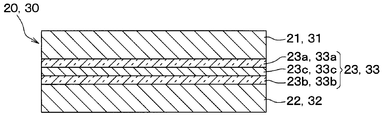
- 1 is a cross-sectional view of a semiconductor device according to a first embodiment. It is sectional drawing which showed the manufacturing process of the 1st heat radiating structure and the 2nd heat radiating structure. It is sectional drawing which showed the manufacturing process of the 1st thermal radiation structure demonstrated in the modification of 1st Embodiment and the 2nd thermal radiation structure. It is sectional drawing of the 1st heat dissipation structure and the 2nd heat dissipation structure with which the semiconductor device concerning 2nd Embodiment is equipped. It is sectional drawing which showed the manufacturing process of the 1st heat radiating structure and the 2nd heat radiating structure.
- the semiconductor device 100 of this embodiment includes a semiconductor chip 10, a first heat dissipation structure 20, a second heat dissipation structure 30, and a heat dissipation block 40, and a bonding material 50 that joins them, A mold resin 60 for sealing them is provided.
- the lower surface of the semiconductor chip 10 and the upper surface of the first heat dissipating structure 20 between the lower surface of the semiconductor chip 10 and the upper surface of the first heat dissipating structure 20 are defined as the lower surface of the semiconductor chip 10 located on the lower side of the paper. Bonded by the bonding material 50. Further, the upper surface of the semiconductor chip 10 and the lower surface of the heat dissipation block 40 are also bonded via the bonding material 50. Further, the heat dissipation block 40 and the second heat dissipation structure 30 are also bonded by the bonding material 50.
- the bonding material 50 is made of a conductive material such as solder, and the semiconductor chip 10, the first heat dissipation structure 20, the second heat dissipation structure 30, and the heat dissipation block 40 are physically connected to each other. In addition, both are electrically connected.
- a material other than solder for example, a conductive adhesive or the like can also be used.
- the bonding material 50 is made of a material that is not a conductive material. May be.
- heat is radiated on the upper surface of the semiconductor chip 10 via the bonding material 50, the heat dissipation block 40, the bonding material 50, and the second heat dissipation structure 30, and from the bonding material 50 on the lower surface of the semiconductor chip 10. Heat is radiated through the first heat radiating structure 20.
- the semiconductor chip 10 corresponds to a heat generating component in which a heat generating element or the like is formed.
- the heating element include a power semiconductor element such as a vertical IGBT (insulated gate bipolar transistor), a MOSFET, and a diode.
- the semiconductor chip 10 includes a vertical IGBT or MOSFET as a heating element.
- the semiconductor chip 10 is, for example, a rectangular thin plate.
- a heat dissipation block 40 is joined to a part of the upper surface of the semiconductor chip 10, and a lead frame 70 that constitutes a control terminal is electrically connected via a bonding wire 80 outside the heat dissipation block 40.
- the lead frame 70 is connected to the gate, and the heat dissipation block 40 is a surface electrode, that is, an emitter electrode in the case of an IGBT or a source electrode in the case of a MOSFET. Connected to.
- the entire back surface of the semiconductor chip 10 is connected to the first heat dissipation structure 20. Thereby, for example, the back electrode of the semiconductor chip 10 and the first heat dissipation structure 20 are connected.
- the first heat dissipation structure 20 has a structure in which a first heat sink 21 and a second heat sink 22 corresponding to a first metal layer and a second metal layer are bonded via a bonding material 23, and has a flat plate shape. .
- the first heat sink 21 forms a surface to be bonded to the semiconductor chip 10 in the first heat dissipation structure 20.
- the first heat sink 21 is physically and via the bonding material 50 on the lower surface side of the semiconductor chip 10. Electrically connected.
- the second heat sink 22 is disposed on the opposite side to the semiconductor chip 10 with the first heat sink 21 interposed therebetween in the first heat dissipation structure 20.
- the bonding material 23 has a function of insulating the first heat sink 21 and the second heat sink 22 while bonding the first heat sink 21 and the second heat sink 22.
- the first heat sink 21 and the second heat sink 22 are made of a material having a high heat transfer coefficient, and are made of a metal such as copper or aluminum.
- the first heat sink 21 also constitutes a current path that flows through the semiconductor chip 10.
- the first heat sink 21 is provided with a lead portion 21 a drawn to the outside of the mold resin 60, and the back surface of the semiconductor chip 10 can be electrically connected to the outside through the first heat sink 21.
- the lead part 21 a is drawn out in one direction of the surface direction with respect to the surface of the first heat sink 21.
- the surface of the first heat dissipation structure 20 opposite to the semiconductor chip 10, that is, the lower surface of the second heat sink 22 is exposed from the mold resin 60. By making this lower surface a heat radiating surface, heat emitted from the semiconductor chip 10 is released.
- the bonding material 23 insulates the first heat sink 21 and the second heat sink 22 while bonding them.
- the bonding material 23 is composed of a thin-film-like inorganic material layer, and in the present embodiment, is composed of glass that is an inorganic material.
- the thin film of the bonding material 23 made of glass is set in accordance with the constituent materials of the first heat sink 21 and the second heat sink 22, and the linear expansion coefficient of the bonding material 23 has the first heat sink 21 and the second heat sink 22. To approximate. For example, when the constituent material of the first heat sink 21 and the second heat sink 22 is copper, the linear expansion coefficient of copper is about 17 ppm / ° C.
- the thickness of the bonding material 23 is set so that the linear expansion coefficient obtained by synthesizing the entire first heat dissipation structure 20 including the bonding material 23 approaches 17 ppm / ° C., for example, the bonding material 23 is in the order of nm. It is thin. In this way, the linear expansion coefficient of the bonding material 23 is approximated to the linear expansion coefficient of the first heat sink 21 and the second heat sink 22. As a result, even when the first heat dissipation structure 20 is sealed in the mold resin 60, it is possible to suppress cracks due to thermal stress caused by the difference in linear expansion coefficient, and to achieve a heat dissipation structure with high reliability. Become.
- the second heat dissipating structure 30 has a structure in which a first heat sink 31 and a second heat sink 32 corresponding to the first metal layer and the second metal layer are bonded via a bonding material 33, and has a flat plate shape.
- the first heat sink 31 constitutes the surface of the second heat dissipation structure 30 that is bonded to the semiconductor chip 10.
- the first heat sink 31 is connected to the upper surface side of the semiconductor chip 10 via the bonding material 50 and the heat dissipation block 40. Are physically and electrically connected.
- the second heat sink 32 is disposed on the opposite side to the semiconductor chip 10 with the first heat sink 31 interposed therebetween in the second heat dissipation structure 30.
- the bonding material 33 has a function of insulating the first heat sink 31 and the second heat sink 32 while bonding them.
- the first heat sink 31 and the second heat sink 32 are made of a material having a high heat transfer coefficient, and are made of a metal such as copper or aluminum, for example.
- the first heat sink 31 also constitutes a current path that flows through the semiconductor chip 10.
- the first heat sink 31 is provided with a lead portion 31 a drawn to the outside of the mold resin 60, and the upper surface of the semiconductor chip 10 can be electrically connected to the outside through the first heat sink 31.
- the lead part 31 a is drawn out in one direction of the surface direction with respect to the surface of the first heat sink 31.
- the surface of the second heat dissipation structure 30 opposite to the semiconductor chip 10, that is, the upper surface of the second heat sink 32 is exposed from the mold resin 60. By making this upper surface also a heat radiating surface, the heat generated by the semiconductor chip 10 is released.
- the bonding material 33 is the same as the bonding material 23 provided in the first heat dissipation structure 20. Also for the second heat dissipation structure 30, the thickness of the bonding material 33 is set so that the linear expansion coefficient obtained by synthesizing the entire second heat dissipation structure 30 including the bonding material 33 approaches 17 ppm / ° C. For this reason, the 2nd heat dissipation structure 30 is also a heat dissipation structure from which high reliability is acquired.
- the mold resin 60 seals the semiconductor chip 10, the first heat dissipation structure 20, the second heat dissipation structure 30, the heat dissipation block 40, and the like. From the mold resin 60, the lower surface of the second heat sink 22 and one end of the lead portion 21a in the first heat dissipation structure 20, the upper surface of the second heat sink 32 and one end of the lead portion 31a in the second heat dissipation structure 30, and the lead frame 70 Some are exposed. The exposed end portions of the lead portion 21a, the lead portion 31a, and the lead frame 70 can be electrically connected to the outside. Further, the heat generated by the semiconductor chip 10 is released by using the exposed lower surface of the second heat sink 22 and the upper surface of the second heat sink 32 as a heat radiating surface.
- the lead frame 70 is connected to a desired location on the upper surface of the semiconductor chip 10 via the bonding wire 80 as described above.
- the joint portion by the bonding wire 80 is covered with the mold resin 60, and the tip position of the lead frame 70 is exposed from the mold resin 60 rather than the joint portion with the bonding wire 80.
- the semiconductor device 100 is configured by the structure as described above.
- the semiconductor device 100 configured as described above is used for an inverter circuit in an automobile, for example. Since the semiconductor chip 10 generates heat during use, the semiconductor device 100 is attached to, for example, a cooler (not shown) in order to release the heat, and the exposed surfaces of the second heat sinks 22 and 32 serve as refrigerant in the cooler. Assembled to be exposed.
- the exposed surface exposed to the refrigerant in the cooler needs to be insulated from the semiconductor chip 10.
- the bonding materials 23 and 33 of the first heat dissipation structure 20 and the second heat dissipation structure 30 are made of an inorganic material, specifically glass. Insulation between the semiconductor chip 10 and the exposed surface can be ensured.
- the bonding materials 23 and 33 are made of an inorganic material, the linear expansion coefficient can be approximated to the first heat sinks 21 and 31 and the second heat sinks 22 and 32 as compared with the case where the bonding materials 23 and 33 are made of ceramics. It becomes possible. Furthermore, even if it does not contain a filler like the case where the joining materials 23 and 33 are comprised with resin, it has high heat dissipation. For this reason, it is possible to achieve both heat dissipation and insulating properties without requiring solder for relaxing the thermal stress of the bonding materials 23 and 33 serving as insulating materials.
- the semiconductor device 100 having such a structure is basically manufactured by the same manufacturing method as the conventional one, and only the manufacturing process of the first heat radiating structure 20 and the second heat radiating structure 30 is different from the conventional one.
- the first heat dissipation structure 20 and the second heat dissipation structure 30 are manufactured by, for example, a method as shown in FIG. First, bonding materials 23 and 33 made of an inorganic material such as glass are attached to the lower surfaces of the first heat sinks 21 and 31. Then, the first heat sinks 21 and 31 are installed so that the bonding materials 23 and 33 are directed to the upper surfaces of the second heat sinks 22 and 32, and the first heat sinks 21 and 31 are interposed via the bonding materials 23 and 33 by thermocompression bonding or the like. 31 and the second heat sinks 22 and 32 are joined. Thereby, the 1st thermal radiation structure 20 and the 2nd thermal radiation structure 30 can be manufactured. Here, the bonding materials 23 and 33 are attached to the lower surface side of the first heat sinks 21 and 31, but the bonding materials 23 and 33 may be attached to the upper surface side of the second heat sinks 22 and 32. good.
- the bonding property between the metal material and the inorganic material constituting the first heat sink 21 or the second heat sink 22 is low, the surface on the bonding material 23 side of the first heat sink 21 or the second heat sink 22 is flattened. After the treatment, plasma treatment is performed. In this way, it becomes possible to improve the bonding property between the first heat sink 21 or the second heat sink 22 and the bonding material 23.
- a first heat sink 21 is prepared by bonding a bonding material 23 made of an inorganic material, and the second heat sink 22 is bonded to the bonding material 23 by first bonding.
- a heat dissipation structure 20 was manufactured.
- the second heat dissipation structure 30 was also manufactured by the same method.
- a part of the bonding materials 23 and 33 made of an inorganic material is formed thinly on the lower surfaces of the first heat sinks 21 and 31 and the upper surfaces of the second heat sinks 22 and 32, respectively. Keep it. And you may manufacture the 1st heat radiating structure 20 and the 2nd heat radiating structure 30 by bonding those parts together by solid phase bonding etc. Also as such a manufacturing method, the 1st heat dissipation structure 20 and the 2nd heat dissipation structure 30 of the structure similar to 1st Embodiment can be manufactured.
- the bonding materials 23 and 33 of the first heat dissipation structure 20 and the second heat dissipation structure 30 are not only inorganic materials but also inorganic materials and the first heat sinks 21, 31 or second.
- a material for assisting the joining to the heat sinks 22 and 32 is provided.
- portions of the bonding materials 23 and 33 that are disposed on the first heat sink 21 or 31 or second heat sink 22 or 32 side are inorganic material layers 23a, 23b, 33a, and 33b, and the bonding film 23c, 33c is arranged.
- the bonding film 23c a material having good bonding properties with the inorganic material layers 23a, 23b, 33a, and 33b, for example, a conductive material such as gold or copper is used.
- Inorganic material layers 23a, 23b, 33a, and 33b may be difficult to bond to each other, but by providing bonding films 23c and 33c between inorganic material layers 23a, 23b, 33a, and 33b as in this embodiment, bonding is possible. Becomes easier. Even with such a structure, the same effect as in the first embodiment can be obtained.
- the bonding films 23c and 33c are made of a conductive material
- part of the bonding materials 23 and 33 is made of a conductive material. Even in this case, the insulating properties can be ensured by the inorganic material layers 23a, 23b, 33a, and 33b.
- the first heat dissipation structure 20 and the second heat dissipation structure 30 having such a configuration can be manufactured as follows. First, as shown in FIG. 5, inorganic material layers 23 a, 23 b, 33 a, and 33 b are thinly formed on the lower surfaces of the first heat sinks 21 and 31 and the upper surfaces of the second heat sinks 22 and 32, respectively. Further, a part of the bonding films 23c and 33c is formed thin on the surface of each inorganic material layer 23a, 23b, 33a and 33b. Then, for example, the bonding films 23 c and 33 c are bonded together by thermocompression bonding by pressing the first heat sinks 21 and 31 and the second heat sinks 22 and 32. With such a manufacturing method, the first heat dissipation structure 20 and the second heat dissipation structure 30 of the present embodiment can be manufactured.
- the bonding materials 23 and 33 of the first heat dissipation structure 20 and the second heat dissipation structure 30 are not limited to the inorganic material, but the inorganic material and the first heat sinks 21, 31 or the second heat sink 21.
- a material for assisting the joining to the heat sinks 22 and 32 is provided.
- the first heat sinks 21 and 31 are the inorganic material layers 23d and 33d
- the bonding films 23e and 33e are disposed on the second heat sinks 22 and 32 side.
- a material having good bonding properties with the inorganic material layers 23d and 33d for example, a conductive material such as gold or copper is used.
- the inorganic material layers 23d and 33d are directly bonded to the heat sink material by thermocompression bonding or the like, it may be difficult to bond them. However, bonding is facilitated by providing the bonding films 23e and 33e between the inorganic material layers 23d and 33d and the second heat sinks 22 and 32 as in the present embodiment. Even with such a structure, the same effect as in the first embodiment can be obtained.
- the bonding films 23e and 33e are made of a conductive material
- part of the bonding materials 23 and 33 is made of a conductive material. Even in this case, insulation can be ensured by the inorganic material layers 23d and 33d.
- the inorganic material layers 23d and 33d are arranged on the first heat sinks 21 and 31 side, and the bonding films 23e and 33e are arranged on the second heat sinks 22 and 32 side. good.
- the first heat dissipation structure 20 and the second heat dissipation structure 30 having such a configuration can be manufactured as follows. First, as shown in FIG. 7, inorganic material layers 23d and 33d and bonding films 23e and 33e are formed on the lower surfaces of the first heat sinks 21 and 31, respectively. Then, the second heat sinks 22 and 32 are arranged so as to face the bonding films 23e and 33e, and the bonding films 23e and 33e are pressed into the second heat sink by pressing the first heat sinks 21 and 31 and the second heat sinks 22 and 32, for example. Bond to 22 and 32 by thermocompression bonding. With such a manufacturing method, the first heat dissipation structure 20 and the second heat dissipation structure 30 of the present embodiment can be manufactured.
- first and second heat sinks 22 and 32 may be configured by a part of the cooler, or may have a structure in which radiating fins and the like are integrated.
- the inorganic material layer included in the bonding material is made of glass
- it may be made of an inorganic material other than glass.
- the inorganic material layer may be made of an amorphous material such as deformable low-elasticity ceramic.
- the low-elasticity ceramic for example, a flexible film-like ceramic manufactured by EUREKITE can be used.
Landscapes
- Cooling Or The Like Of Semiconductors Or Solid State Devices (AREA)
Abstract
第1放熱構造体(20)および第2放熱構造体(30)の接合材(23、33)を無機材料、例えばガラスで構成する。このように、無機材料にて構成される接合材(23、33)を用いても、半導体チップ(10)と露出面との絶縁性を確保できる。また、セラミックスで構成する場合と比較して、線膨張係数を第1ヒートシンク(21、31)や第2ヒートシンク(22、32)に近似させることが可能となる。さらに、接合材(23、33)を樹脂で構成する場合のようにフィラーを含有させなくても高い放熱性を有している。このため、絶縁材となる接合材(23、33)の熱応力緩和のためのはんだを要しなくても、放熱性と絶縁性の両立を図ることが可能となる。
Description
本出願は、2016年6月14日に出願された日本特許出願番号2016-118257号に基づくもので、ここにその記載内容が参照により組み入れられる。
本開示は、放熱機能を有する絶縁構造体を備えた半導体装置に関するものである。
発熱素子を有する半導体装置では、高温化を抑制するために、発熱素子が発した熱を放出させる必要がある。このため、発熱素子を金属製のヒートシンクに貼り付け、ヒートシンクを介して効率的に放熱が行われるようにしている。ただし、発熱素子と外部との絶縁を図ることが必要となることから、ヒートシンクを2枚重ねの構造とし、2枚のヒートシンクの間に絶縁材を挟むことで絶縁構造体を構成している。
絶縁構造体としては、2枚のヒートシンクの間に絶縁材として樹脂材料を挟み込む構造(以下、第1絶縁構造という)や、特許文献1に示されるように、2枚のヒートシンクの間にセラミックスを挟み込む構造(以下、第2絶縁構造という)がある。
第1絶縁構造のように絶縁材として樹脂材料を適用する場合、樹脂材料の放熱性が低いことから、熱伝達率を高めるために樹脂材料にフィラーを多量に含有させる必要がある。フィラーの含有量を増やすほど放熱性が向上するが、絶縁性が低下することから、放熱性と絶縁性とがトレードオフの関係となり、両者を共に向上させることは難しい。また、第1絶縁構造では、樹脂成分の劣化や吸水性に基づく湿度等に対する信頼性の低下が懸念される。
一方、第2絶縁構造のように絶縁材としてセラミックスを適用する場合、放熱性と絶縁性の両方を得ることができる。ところが、セラミックスの線膨張係数がヒートシンクを構成する銅などの金属材料の線膨張係数と大きく異なることから、セラミックスとヒートシンクとの線膨張係数差に起因する熱応力緩和の為に、はんだをセラミックスとヒートシンクとの間に配置する必要がある。このように熱応力緩和用の材料が必要になるし、製品の製造コスト増大を招くことになる。
本開示は上記点に鑑みて、絶縁材の熱応力緩和のためのはんだを要しなくても、放熱性と絶縁性の両立を図ることができる絶縁構造体を有する半導体装置を提供することを目的とする。
本開示の1つの観点における半導体装置は、板状の半導体チップと、半導体チップの少なくとも一面側に配置され、半導体チップで発した熱を放出させる放熱構造体と、を有し、放熱構造体は、半導体チップ側に配置される第1金属層と、第1金属層に対して半導体チップと反対側に配置される第2金属層と、第1金属層と第2金属層との間に配置された接合材と、を有し、接合材は、無機材料層を含み、該無機材料層によって第1金属層と第2金属層との間が絶縁されている。
このように、放熱構造体に無機材料層、例えばガラスを含む接合材を用いるようにしている。このため、半導体チップと露出面との絶縁性を確保することが可能となる。また、接合材を無機材料層を含む構成としていることから、セラミックスで構成する場合と比較して、線膨張係数を第1金属層や第2金属層に近似させることが可能となる。さらに、接合材を樹脂で構成する場合のようにフィラーを含有させなくても高い放熱性を有している。このため、絶縁材となる接合材の熱応力緩和のためのはんだを要しなくても、放熱性と絶縁性の両立を図ることが可能となる。
以下、本開示の実施形態について図に基づいて説明する。なお、以下の各実施形態相互において、互いに同一もしくは均等である部分には、同一符号を付して説明を行う。
(第1実施形態)
第1実施形態について説明する。まず、図1を参照して、本実施形態にかかる半導体装置の構成について説明する。
第1実施形態について説明する。まず、図1を参照して、本実施形態にかかる半導体装置の構成について説明する。
図1に示すように、本実施形態の半導体装置100は、半導体チップ10、第1放熱構造体20、第2放熱構造体30および放熱ブロック40と、これらの間を接合する接合材50と、これらを封止するモールド樹脂60などを備えて構成されている。
具体的には、半導体チップ10のうち紙面下方に位置する一面側を下面、紙面上方に位置する他面側を上面として、半導体チップ10の下面と第1放熱構造体20の上面との間は接合材50によって接合されている。また、半導体チップ10の上面と放熱ブロック40の下面との間も接合材50を介して接合されている。さらに、放熱ブロック40と第2放熱構造体30との間も接合材50によって接合されている。
本実施形態の場合、接合材50は導電材料であるはんだ等によって構成されており、半導体チップ10、第1放熱構造体20、第2放熱構造体30および放熱ブロック40の相互間が物理的にも電気的にも接続された形態とされている。なお、接合材50としては、はんだ以外のもの、例えば導電性接着剤等を用いることもでき、電気的な接続を行わずに物理的な接合のみを行う場合には、導電材料でない材料で構成されていても良い。
このような構成により、半導体チップ10の上面では、接合材50、放熱ブロック40、接合材50および第2放熱構造体30を介して放熱が行われ、半導体チップ10の下面では、接合材50から第1放熱構造体20を介して放熱が行われるようになっている。
半導体チップ10は、発熱素子などが形成された発熱部品に相当するものである。発熱素子としては、例えば縦型のIGBT(絶縁ゲート型バイポーラトランジスタ)やMOSFET、ダイオード等のパワー半導体素子が挙げられる。本実施形態の場合、半導体チップ10には、発熱素子として縦型のIGBTやMOSFETが備えてある。
半導体チップ10は、例えば矩形状の薄板状とされている。そして、半導体チップ10の上面における一部に放熱ブロック40が接合され、放熱ブロック40よりも外側において制御端子を構成するリードフレーム70がボンディングワイヤ80を介して電気的に接続されている。例えば、半導体チップ10に対して縦型のIGBTやMOSFETを備えている場合、リードフレーム70はゲートに接続され、放熱ブロック40は表面電極、すなわちIGBTの場合のエミッタ電極やMOSFETの場合のソース電極に接続される。一方、半導体チップ10の裏面については全面が第1放熱構造体20に接続されている。これにより、例えば半導体チップ10の裏面電極と第1放熱構造体20とが接続される。
第1放熱構造体20は、第1金属層および第2金属層に相当する第1ヒートシンク21と第2ヒートシンク22とが接合材23を介して接合された構造とされ、平板状とされている。第1ヒートシンク21は、第1放熱構造体20のうち半導体チップ10に接合される表面を構成しており、本実施形態の場合は半導体チップ10の下面側に接合材50を介して物理的および電気的に接続されている。第2ヒートシンク22は、第1放熱構造体20のうち第1ヒートシンク21を挟んで半導体チップ10と反対側に配置されている。接合材23は、第1ヒートシンク21と第2ヒートシンク22との間を接合しつつ、これらの間を絶縁する機能を有している。
第1ヒートシンク21および第2ヒートシンク22は、熱伝達率の高い材質で構成されており、例えば銅やアルミニウムなどの金属によって構成されている。本実施形態の場合、第1ヒートシンク21は、半導体チップ10に流れる電流経路も構成している。具体的には、第1ヒートシンク21にはモールド樹脂60の外部まで引き出されたリード部21aが備えられ、第1ヒートシンク21を通じて半導体チップ10の裏面が外部と電気的に接続可能となっている。リード部21aは、第1ヒートシンク21の表面に対する面方向の一方向に引き出されている。
また、第1放熱構造体20のうち半導体チップ10と反対側の表面、つまり第2ヒートシンク22の下面はモールド樹脂60から露出させられている。この下面が放熱面とされることで、半導体チップ10で発した熱の放出が行われる。
接合材23は、第1ヒートシンク21と第2ヒートシンク22とを接合しつつ、これらの間を絶縁する。具体的には、接合材23を薄膜状の無機材料層によって構成しており、本実施形態の場合には無機材料であるガラスで構成している。ガラスで構成した接合材23の薄膜は、第1ヒートシンク21や第2ヒートシンク22の構成材料に合わせて薄さなどが設定され、接合材23の線膨張係数が第1ヒートシンク21や第2ヒートシンク22と近似するようにしている。例えば、第1ヒートシンク21や第2ヒートシンク22の構成材料が銅である場合、銅の線膨張係数が17ppm/℃程度である。このため、接合材23を含めた第1放熱構造体20の全体を合成した線膨張係数が17ppm/℃に近づくように接合材23の薄さなどを設定し、例えば接合材23をnmオーダの薄さとしている。このようにすることで、接合材23の線膨張係数を第1ヒートシンク21や第2ヒートシンク22の線膨張係数と近似させている。これにより、第1放熱構造体20をモールド樹脂60に封止しても、線膨張係数差に起因する熱応力によるクラックなどを抑制でき、高い信頼性が得られる放熱構造とすることが可能となる。
同様に、第2放熱構造体30は、第1金属層および第2金属層に相当する第1ヒートシンク31と第2ヒートシンク32とが接合材33を介して接合された構造とされ、平板状とされている。第1ヒートシンク31は、第2放熱構造体30のうち半導体チップ10に接合される表面を構成しており、本実施形態の場合は半導体チップ10の上面側に接合材50や放熱ブロック40を介して物理的および電気的に接続されている。第2ヒートシンク32は、第2放熱構造体30のうち第1ヒートシンク31を挟んで半導体チップ10と反対側に配置されている。接合材33は、第1ヒートシンク31と第2ヒートシンク32との間を接合しつつ、これらの間を絶縁する機能を有している。
第1ヒートシンク31および第2ヒートシンク32は、熱伝達率の高い材質で構成されており、例えば銅やアルミニウムなどの金属によって構成されている。本実施形態の場合、第1ヒートシンク31は、半導体チップ10に流れる電流経路も構成している。具体的には、第1ヒートシンク31にはモールド樹脂60の外部まで引き出されたリード部31aが備えられ、第1ヒートシンク31を通じて半導体チップ10の上面が外部と電気的に接続可能となっている。リード部31aは、第1ヒートシンク31の表面に対する面方向の一方向に引き出されている。
また、第2放熱構造体30のうち半導体チップ10と反対側の表面、つまり第2ヒートシンク32の上面はモールド樹脂60から露出させられている。この上面も放熱面とされることで、半導体チップ10で発した熱の放出が行われる。
接合材33については、第1放熱構造体20に備えられる接合材23と同様のものとされている。第2放熱構造体30についても、接合材33を含めた第2放熱構造体30の全体を合成した線膨張係数が17ppm/℃に近づくように接合材33の薄さなどを設定している。このため、第2放熱構造体30も、高い信頼性が得られる放熱構造となっている。
モールド樹脂60は、半導体チップ10、第1放熱構造体20、第2放熱構造体30および放熱ブロック40などを封止している。モールド樹脂60からは、第1放熱構造体20における第2ヒートシンク22の下面やリード部21aの一端、第2放熱構造体30における第2ヒートシンク32の上面やリード部31aの一端、リードフレーム70の一部が露出させられている。露出させられたリード部21aやリード部31aおよびリードフレーム70の各端部において、外部と電気的に接続可能とされている。また、露出させられた第2ヒートシンク22の下面や第2ヒートシンク32の上面を放熱面として、半導体チップ10で発した熱の放出が行われるようになっている。
なお、リードフレーム70は、上記したように半導体チップ10の上面の所望箇所にボンディングワイヤ80を介して接続されている。ボンディングワイヤ80による接合箇所についてはモールド樹脂60によって覆われており、リードフレーム70のうちボンディングワイヤ80との接合箇所よりも先端位置がモールド樹脂60から露出させられている。
以上のような構造によって、本実施形態にかかる半導体装置100が構成されている。このように構成される半導体装置100は、例えば自動車におけるインバータ回路などに用いられる。そして、使用時には半導体チップ10が熱を発するため、その熱を放出させるために、半導体装置100は例えば図示しない冷却器に取り付けられ、第2ヒートシンク22、32の露出面が冷却器内の冷媒に曝されるように組みつけられる。
このような構成とされる場合、冷却器内の冷媒に曝される露出面が半導体チップ10と絶縁されている必要がある。これに対して、本実施形態にかかる半導体装置100では、第1放熱構造体20および第2放熱構造体30の接合材23、33を無機材料、具体的にはガラスで構成していることから、半導体チップ10と露出面との絶縁性を確保することが可能となる。
また、接合材23、33を無機材料によって構成していることから、セラミックスで構成する場合と比較して、線膨張係数を第1ヒートシンク21、31や第2ヒートシンク22、32に近似させることが可能となる。さらに、接合材23、33を樹脂で構成する場合のようにフィラーを含有させなくても高い放熱性を有している。このため、絶縁材となる接合材23、33の熱応力緩和のためのはんだを要しなくても、放熱性と絶縁性の両立を図ることが可能となる。
このような構造の半導体装置100は、基本的には従来と同様の製造方法によって製造され、第1放熱構造体20および第2放熱構造体30の製造工程についてのみ従来と異なったものとなる。
具体的には、第1放熱構造体20および第2放熱構造体30については、例えば図2に示すような方法によって製造している。まず、第1ヒートシンク21、31の下面側にガラスなどの無機材料で構成される接合材23、33を貼り付ける。そして、第2ヒートシンク22、32の上面側に接合材23、33側を向けるようにして第1ヒートシンク21、31を設置し、熱圧着などによって接合材23、33を介して第1ヒートシンク21、31と第2ヒートシンク22、32とを接合する。これにより、第1放熱構造体20および第2放熱構造体30を製造できる。なお、ここでは、第1ヒートシンク21、31の下面側に接合材23、33を貼り付けるようにしたが、第2ヒートシンク22、32の上面側に接合材23、33を貼り付けるようにしても良い。
このとき、第1ヒートシンク21や第2ヒートシンク22を構成する金属材料と無機材料との接合性が低い場合には、第1ヒートシンク21や第2ヒートシンク22のうち接合材23側の面を平坦化処理した後、プラズマ処理しておく。このようにすれば、第1ヒートシンク21や第2ヒートシンク22と接合材23との接合性を高めることが可能となる。
(第1実施形態の変形例)
第1実施形態では、図2に示したように無機材料で構成された接合材23を貼り付けた第1ヒートシンク21を用意し、接合材23に対して第2ヒートシンク22を接合することで第1放熱構造体20を製造した。第2放熱構造体30についても同様の方法によって製造した。
第1実施形態では、図2に示したように無機材料で構成された接合材23を貼り付けた第1ヒートシンク21を用意し、接合材23に対して第2ヒートシンク22を接合することで第1放熱構造体20を製造した。第2放熱構造体30についても同様の方法によって製造した。
これに対して、図3に示すように、第1ヒートシンク21、31の下面と第2ヒートシンク22、32の上面それぞれに無機材料にて構成される接合材23、33の一部を薄く形成しておく。そして、その一部同士を固相接合などによって貼り合わせることで第1放熱構造体20や第2放熱構造体30を製造しても良い。このような製造方法としても、第1実施形態と同様の構造の第1放熱構造体20および第2放熱構造体30を製造することができる。
(第2実施形態)
第2実施形態について説明する。本実施形態は、第1実施形態に対して第1放熱構造体20および第2放熱構造体30の構成を変更したものであり、その他については第1実施形態と同様であるため、第1実施形態と異なる部分についてのみ説明する。
第2実施形態について説明する。本実施形態は、第1実施形態に対して第1放熱構造体20および第2放熱構造体30の構成を変更したものであり、その他については第1実施形態と同様であるため、第1実施形態と異なる部分についてのみ説明する。
図4に示すように、本実施形態では、第1放熱構造体20および第2放熱構造体30の接合材23、33を無機材料のみではなく、無機材料と第1ヒートシンク21、31もしくは第2ヒートシンク22、32との接合を補助する材料を備えるようにしている。具体的には、接合材23、33のうち第1ヒートシンク21、31もしくは第2ヒートシンク22、32側に配置される部分を無機材料層23a、23b、33a、33bとし、その間に接合膜23c、33cを配置している。接合膜23cとしては、無機材料層23a、23b、33a、33bとの接合性が良い材料、例えば金や銅などの導通材料を用いている。
無機材料層23a、23b、33a、33b同士は接合し難い場合があるが、本実施形態のように無機材料層23a、23b、33a、33bの間に接合膜23c、33cを備えることにより、接合が容易になる。このような構造としても、第1実施形態と同様の効果を得ることができる。
なお、接合膜23c、33cを導通材料で構成する場合、接合材23、33の一部が導通材料で構成されることになる。この場合でも、無機材料層23a、23b、33a、33bによって絶縁性を確保することができる。
このような構成の第1放熱構造体20および第2放熱構造体30については、次のように製造可能である。まず、図5に示すように、第1ヒートシンク21、31の下面と第2ヒートシンク22、32の上面それぞれに無機材料層23a、23b、33a、33bを薄く形成しておく。さらに、各無機材料層23a、23b、33a、33bの表面に接合膜23c、33cの一部を薄く形成しておく。そして、例えば第1ヒートシンク21、31および第2ヒートシンク22、32を押圧することにより接合膜23c、33c同士を熱圧着で貼り合わせる。このような製造方法により、本実施形態の第1放熱構造体20および第2放熱構造体30を製造することができる。
(第3実施形態)
第3実施形態について説明する。本実施形態も、第1実施形態に対して第1放熱構造体20および第2放熱構造体30の構成を変更したものであり、その他については第1実施形態と同様であるため、第1実施形態と異なる部分についてのみ説明する。
第3実施形態について説明する。本実施形態も、第1実施形態に対して第1放熱構造体20および第2放熱構造体30の構成を変更したものであり、その他については第1実施形態と同様であるため、第1実施形態と異なる部分についてのみ説明する。
図6に示すように、本実施形態も、第1放熱構造体20および第2放熱構造体30の接合材23、33を無機材料のみではなく、無機材料と第1ヒートシンク21、31もしくは第2ヒートシンク22、32との接合を補助する材料を備えるようにしている。具体的には、接合材23、33のうち第1ヒートシンク21、31を無機材料層23d、33dとし、第2ヒートシンク22、32側に接合膜23e、33eを配置している。接合膜23e、33eとしては、無機材料層23d、33dとの接合性が良い材料、例えば金や銅などの導通材料を用いている。
無機材料層23d、33dを熱圧着などによって直接ヒートシンク材料に接合しようとすると接合し難い場合がある。しかしながら、本実施形態のように無機材料層23d、33dと第2ヒートシンク22、32との間に接合膜23e、33eを備えることにより、接合が容易になる。このような構造としても、第1実施形態と同様の効果を得ることができる。
なお、接合膜23e、33eを導通材料で構成する場合、接合材23、33の一部が導通材料で構成されることになる。この場合でも、無機材料層23d、33dによって絶縁性を確保することができる。また、ここでは第1ヒートシンク21、31側に無機材料層23d、33dを配置し、第2ヒートシンク22、32側に接合膜23e、33eを配置したが、これらが逆の配置とされていても良い。
このような構成の第1放熱構造体20および第2放熱構造体30については、次のように製造可能である。まず、図7に示すように、第1ヒートシンク21、31の下面に無機材料層23d、33dおよび接合膜23e、33eを形成しておく。そして、第2ヒートシンク22、32を接合膜23e、33eと対向するように配置し、例えば第1ヒートシンク21、31および第2ヒートシンク22、32を押圧することにより接合膜23e、33eを第2ヒートシンク22、32に熱圧着で貼り合わせる。このような製造方法により、本実施形態の第1放熱構造体20および第2放熱構造体30を製造することができる。
(他の実施形態)
本開示は、上記した実施形態に準拠して記述されたが、当該実施形態に限定されるものではなく、様々な変形例や均等範囲内の変形をも包含する。加えて、様々な組み合わせや形態、さらには、それらに一要素のみ、それ以上、あるいはそれ以下、を含む他の組み合わせや形態をも、本開示の範疇や思想範囲に入るものである。
本開示は、上記した実施形態に準拠して記述されたが、当該実施形態に限定されるものではなく、様々な変形例や均等範囲内の変形をも包含する。加えて、様々な組み合わせや形態、さらには、それらに一要素のみ、それ以上、あるいはそれ以下、を含む他の組み合わせや形態をも、本開示の範疇や思想範囲に入るものである。
例えば、上記各実施形態では、放熱機能を有する絶縁構造体を備えた半導体装置の一例を挙げたが、他の構造の半導体装置であっても良い。例えば、上記各実施形態では、半導体チップの上面と下面の両面に放熱構造体を備えた構造を例に挙げたが、少なくとも一面側に放熱構造体が備えられていれば良い。
また、第1ヒートシンク22と第2ヒートシンク23がそれぞれ板状のもので構成された放熱構造体を例に挙げて説明したが、板状である必要はない。例えば、第1、第2ヒートシンク22、32を冷却器の一部によって構成することもできるし、放熱フィンなどが一体となった構造のものとされていても良い。
さらに、接合材に含まれる無機材料層をガラスで構成する場合について説明したが、ガラス以外の無機材料によって構成しても良い。例えば、変形可能な低弾性セラミックスなどのような非結晶材にて無機材料層を構成しても良い。低弾性セラミックスとしては、例えばeurekite社製の柔軟性を有するフィルム状のセラミックスなどを用いることができる。
Claims (5)
- 板状の半導体チップ(10)と、
前記半導体チップの少なくとも一面側に配置され、前記半導体チップで発した熱を放出させる放熱構造体(20、30)と、を有する半導体装置であって、
前記放熱構造体は、前記半導体チップ側に配置される第1金属層(21、31)と、
前記第1金属層に対して前記半導体チップと反対側に配置される第2金属層(22、32)と、
前記第1金属層と前記第2金属層との間に配置された接合材(23、33)と、を有し、
前記接合材は、無機材料層(23a、23b、23d、33a、33b、33d)を含み、該無機材料層によって前記第1金属層と前記第2金属層との間が絶縁されている半導体装置。 - 前記無機材料層はガラスにて構成されている請求項1に記載の半導体装置。
- 前記接合材は、前記無機材料層のみによって構成されている請求項1または2に記載の半導体装置。
- 前記接合材は、前記第1金属層に接する前記無機材料層の一部と、前記第2金属層に接する前記無機材料層の他の一部と、前記一部と前記他の一部との間に配置されている共に前記一部と前記他の一部との間を接合する導通材料にて構成された接合膜(23c、33c)とを有している請求項1に記載の半導体装置。
- 前記接合材は、前記無機材料層(23d、33d)に加えて導通材料にて構成された接合膜(23e、33e)を有し、前記第1金属層側に前記無機材料層が配置されると共に前記第2金属層側に前記接合膜が配置された構造、もしくは、前記第1金属層側に前記接合膜が配置されると共に前記第2金属層側に前記無機材料層が配置された構造とされている請求項1に記載の半導体装置。
Applications Claiming Priority (2)
| Application Number | Priority Date | Filing Date | Title |
|---|---|---|---|
| JP2016118257A JP6638567B2 (ja) | 2016-06-14 | 2016-06-14 | 半導体装置 |
| JP2016-118257 | 2016-06-14 |
Publications (1)
| Publication Number | Publication Date |
|---|---|
| WO2017217149A1 true WO2017217149A1 (ja) | 2017-12-21 |
Family
ID=60663177
Family Applications (1)
| Application Number | Title | Priority Date | Filing Date |
|---|---|---|---|
| PCT/JP2017/017871 Ceased WO2017217149A1 (ja) | 2016-06-14 | 2017-05-11 | 半導体装置 |
Country Status (2)
| Country | Link |
|---|---|
| JP (1) | JP6638567B2 (ja) |
| WO (1) | WO2017217149A1 (ja) |
Cited By (1)
| Publication number | Priority date | Publication date | Assignee | Title |
|---|---|---|---|---|
| US11749632B2 (en) | 2021-03-31 | 2023-09-05 | Toyota Motor Engineering & Manufacturing North America, Inc. | Glass-based bonding structures for power electronics |
Families Citing this family (2)
| Publication number | Priority date | Publication date | Assignee | Title |
|---|---|---|---|---|
| CN111788743B (zh) * | 2018-02-28 | 2021-08-03 | 株式会社村田制作所 | 天线模块 |
| WO2023017570A1 (ja) * | 2021-08-10 | 2023-02-16 | 三菱電機株式会社 | 半導体装置及びインバータユニット |
Citations (2)
| Publication number | Priority date | Publication date | Assignee | Title |
|---|---|---|---|---|
| JP2503778B2 (ja) * | 1988-10-07 | 1996-06-05 | 三菱マテリアル株式会社 | 半導体装置用基板 |
| JP2007300114A (ja) * | 2006-05-02 | 2007-11-15 | Ngk Insulators Ltd | 半導体装置部材及び半導体装置 |
-
2016
- 2016-06-14 JP JP2016118257A patent/JP6638567B2/ja active Active
-
2017
- 2017-05-11 WO PCT/JP2017/017871 patent/WO2017217149A1/ja not_active Ceased
Patent Citations (2)
| Publication number | Priority date | Publication date | Assignee | Title |
|---|---|---|---|---|
| JP2503778B2 (ja) * | 1988-10-07 | 1996-06-05 | 三菱マテリアル株式会社 | 半導体装置用基板 |
| JP2007300114A (ja) * | 2006-05-02 | 2007-11-15 | Ngk Insulators Ltd | 半導体装置部材及び半導体装置 |
Cited By (1)
| Publication number | Priority date | Publication date | Assignee | Title |
|---|---|---|---|---|
| US11749632B2 (en) | 2021-03-31 | 2023-09-05 | Toyota Motor Engineering & Manufacturing North America, Inc. | Glass-based bonding structures for power electronics |
Also Published As
| Publication number | Publication date |
|---|---|
| JP2017224689A (ja) | 2017-12-21 |
| JP6638567B2 (ja) | 2020-01-29 |
Similar Documents
| Publication | Publication Date | Title |
|---|---|---|
| US11862542B2 (en) | Dual side cooling power module and manufacturing method of the same | |
| CN105679720B (zh) | 散热器、包括散热器的电子模块及其制作方法 | |
| JP2016018866A (ja) | パワーモジュール | |
| TW201304061A (zh) | 半導體裝置及佈線基板 | |
| JP6230238B2 (ja) | 半導体装置及びその製造方法 | |
| CN102487053A (zh) | 半导体装置及其制造方法 | |
| TWI648829B (zh) | 半導體裝置的散熱結構 | |
| JP2017139406A (ja) | 半導体装置 | |
| CN111354710B (zh) | 半导体装置及其制造方法 | |
| CN207381382U (zh) | 电力电子模块和电力电子元器件封装基板 | |
| JP2016004941A (ja) | 半導体装置及びパワーモジュール | |
| WO2017217149A1 (ja) | 半導体装置 | |
| WO2013121521A1 (ja) | 半導体装置 | |
| JP2010192591A (ja) | 電力用半導体装置とその製造方法 | |
| CN104798194B (zh) | 半导体器件 | |
| JP6095303B2 (ja) | 半導体装置および半導体装置の製造方法 | |
| CN110098178A (zh) | 半导体器件 | |
| JP7170614B2 (ja) | 半導体装置 | |
| JP5975866B2 (ja) | 電力用半導体装置 | |
| JP5840102B2 (ja) | 電力用半導体装置 | |
| WO2021006297A1 (ja) | 半導体パッケージ、電子装置、および半導体パッケージの製造方法 | |
| JP7008842B2 (ja) | 半導体装置および半導体装置の製造方法 | |
| JP2013179231A (ja) | 半導体モジュール | |
| JP6274019B2 (ja) | 半導体装置及びその製造方法 | |
| JP2009016380A (ja) | 半導体装置及びその製造方法 |
Legal Events
| Date | Code | Title | Description |
|---|---|---|---|
| 121 | Ep: the epo has been informed by wipo that ep was designated in this application |
Ref document number: 17813054 Country of ref document: EP Kind code of ref document: A1 |
|
| NENP | Non-entry into the national phase |
Ref country code: DE |
|
| 122 | Ep: pct application non-entry in european phase |
Ref document number: 17813054 Country of ref document: EP Kind code of ref document: A1 |