WO2017208702A1 - 撮像素子及び撮像装置 - Google Patents
撮像素子及び撮像装置 Download PDFInfo
- Publication number
- WO2017208702A1 WO2017208702A1 PCT/JP2017/016820 JP2017016820W WO2017208702A1 WO 2017208702 A1 WO2017208702 A1 WO 2017208702A1 JP 2017016820 W JP2017016820 W JP 2017016820W WO 2017208702 A1 WO2017208702 A1 WO 2017208702A1
- Authority
- WO
- WIPO (PCT)
- Prior art keywords
- pixel
- phase difference
- difference detection
- pixels
- signal
- Prior art date
- Legal status (The legal status is an assumption and is not a legal conclusion. Google has not performed a legal analysis and makes no representation as to the accuracy of the status listed.)
- Ceased
Links
Images








Classifications
-
- G—PHYSICS
- G02—OPTICS
- G02B—OPTICAL ELEMENTS, SYSTEMS OR APPARATUS
- G02B7/00—Mountings, adjusting means, or light-tight connections, for optical elements
- G02B7/28—Systems for automatic generation of focusing signals
- G02B7/34—Systems for automatic generation of focusing signals using different areas in a pupil plane
-
- G—PHYSICS
- G03—PHOTOGRAPHY; CINEMATOGRAPHY; ANALOGOUS TECHNIQUES USING WAVES OTHER THAN OPTICAL WAVES; ELECTROGRAPHY; HOLOGRAPHY
- G03B—APPARATUS OR ARRANGEMENTS FOR TAKING PHOTOGRAPHS OR FOR PROJECTING OR VIEWING THEM; APPARATUS OR ARRANGEMENTS EMPLOYING ANALOGOUS TECHNIQUES USING WAVES OTHER THAN OPTICAL WAVES; ACCESSORIES THEREFOR
- G03B13/00—Viewfinders; Focusing aids for cameras; Means for focusing for cameras; Autofocus systems for cameras
- G03B13/32—Means for focusing
- G03B13/34—Power focusing
- G03B13/36—Autofocus systems
-
- H—ELECTRICITY
- H04—ELECTRIC COMMUNICATION TECHNIQUE
- H04N—PICTORIAL COMMUNICATION, e.g. TELEVISION
- H04N23/00—Cameras or camera modules comprising electronic image sensors; Control thereof
- H04N23/60—Control of cameras or camera modules
- H04N23/67—Focus control based on electronic image sensor signals
- H04N23/672—Focus control based on electronic image sensor signals based on the phase difference signals
-
- H—ELECTRICITY
- H04—ELECTRIC COMMUNICATION TECHNIQUE
- H04N—PICTORIAL COMMUNICATION, e.g. TELEVISION
- H04N23/00—Cameras or camera modules comprising electronic image sensors; Control thereof
- H04N23/80—Camera processing pipelines; Components thereof
- H04N23/84—Camera processing pipelines; Components thereof for processing colour signals
-
- H—ELECTRICITY
- H04—ELECTRIC COMMUNICATION TECHNIQUE
- H04N—PICTORIAL COMMUNICATION, e.g. TELEVISION
- H04N25/00—Circuitry of solid-state image sensors [SSIS]; Control thereof
- H04N25/10—Circuitry of solid-state image sensors [SSIS]; Control thereof for transforming different wavelengths into image signals
- H04N25/11—Arrangement of colour filter arrays [CFA]; Filter mosaics
- H04N25/13—Arrangement of colour filter arrays [CFA]; Filter mosaics characterised by the spectral characteristics of the filter elements
- H04N25/134—Arrangement of colour filter arrays [CFA]; Filter mosaics characterised by the spectral characteristics of the filter elements based on three different wavelength filter elements
-
- H—ELECTRICITY
- H04—ELECTRIC COMMUNICATION TECHNIQUE
- H04N—PICTORIAL COMMUNICATION, e.g. TELEVISION
- H04N25/00—Circuitry of solid-state image sensors [SSIS]; Control thereof
- H04N25/70—SSIS architectures; Circuits associated therewith
-
- H—ELECTRICITY
- H04—ELECTRIC COMMUNICATION TECHNIQUE
- H04N—PICTORIAL COMMUNICATION, e.g. TELEVISION
- H04N25/00—Circuitry of solid-state image sensors [SSIS]; Control thereof
- H04N25/70—SSIS architectures; Circuits associated therewith
- H04N25/703—SSIS architectures incorporating pixels for producing signals other than image signals
- H04N25/704—Pixels specially adapted for focusing, e.g. phase difference pixel sets
-
- H—ELECTRICITY
- H04—ELECTRIC COMMUNICATION TECHNIQUE
- H04N—PICTORIAL COMMUNICATION, e.g. TELEVISION
- H04N23/00—Cameras or camera modules comprising electronic image sensors; Control thereof
- H04N23/80—Camera processing pipelines; Components thereof
- H04N23/84—Camera processing pipelines; Components thereof for processing colour signals
- H04N23/843—Demosaicing, e.g. interpolating colour pixel values
Definitions
- the present invention relates to an imaging element and an imaging apparatus.
- imaging devices such as CCD (Charge Coupled Device) image sensors or CMOS (Complementary Metal Oxide Semiconductor) image sensors
- imaging functions such as digital still cameras, digital video cameras, and mobile phones including smartphones.
- the demand for information equipment is increasing rapidly.
- an information device having the above imaging function is referred to as an imaging device.
- These imaging apparatuses employ a phase difference AF (Auto Focus) method (see Patent Documents 1 and 2) as a focusing control method for focusing on a main subject.
- AF Auto Focus
- a pair of phase difference detection pixels in which photoelectric conversion areas are eccentric in opposite directions are discretely provided on the entire light receiving surface. are used (see Patent Documents 1 and 2).
- Patent Document 1 a phase difference detection pixel arranged at a position where a pixel for photoelectrically converting blue light and a pixel arranged for photoelectric conversion of green light are arranged at positions where the pixels should be arranged.
- An imaging device having a pair with a phase difference detection pixel is described.
- Patent Document 2 has a pair of phase difference detection pixels for detecting a phase difference in the horizontal direction and a pair of phase difference detection pixels for detecting a phase difference in the vertical direction.
- An image sensor is described in which a pair of is arranged on a light receiving surface.
- the phase difference detection pixel has a photoelectric conversion area smaller than other normal pixels (imaging pixels). For this reason, it becomes insufficient to use the output signal of the phase difference detection pixel as a pixel signal for generating captured image data. Therefore, it is necessary to correct the output signal of the phase difference detection pixel.
- interpolation is performed by generating a pixel signal corresponding to the position of the phase difference detection pixel using the output signals of the imaging pixels around the phase difference detection pixel. There is a correction.
- the gain corresponding to the sensitivity ratio between the phase difference detection pixel and the imaging pixel near the pixel is multiplied by the output signal of the phase difference detection pixel to position the phase difference detection pixel.
- interpolation is performed using the output signal of the imaging pixel at a position different from the phase difference detection pixel on the light receiving surface. For this reason, when a fine pattern subject or the like is imaged, the quality of the captured image may be reduced by the correction.
- a color captured image signal output from an image sensor is subjected to image processing and converted into captured image data including a luminance signal and a color difference signal.
- the role of color difference is small compared to luminance, and even if the resolution of the color difference signal is lowered, it does not feel as if the image quality has dropped much. That is, the quality of the captured image data is determined by the quality of the luminance signal.
- phase difference detection pixel is a pixel in which the photoelectric conversion region is decentered in the phase difference detection direction, the level of the output signal varies depending on the position on the light receiving surface.
- the phase difference detection pixel in which the photoelectric conversion region is eccentric in the right direction is defined as the right eccentric pixel.
- the output signal of the right eccentric pixel near the left end of the light receiving surface is smaller than the output signal of the right eccentric pixel near the right end of the light receiving surface.
- Such an output signal difference tends to increase as the imaging lens widens or the size of the light receiving surface increases.
- phase difference detection pixels near the edge of the light receiving surface have levels that can be used as pixel signals for generating captured image data even if the output signal is gain-corrected. It becomes difficult to return.
- Patent Documents 1 and 2 do not consider the above-described problems when performing gain correction.
- the present invention has been made in view of the above circumstances, and it is possible to employ gain correction as a correction method of an output signal of a phase difference detection pixel that maximizes the contribution to a luminance signal, thereby improving captured image quality. It is an object of the present invention to provide an image pickup device that can be operated and an image pickup apparatus including the image pickup device.
- the image sensor of the present invention is an image sensor having a plurality of pixels that photoelectrically convert light of different colors, and having a light receiving surface in which the plurality of pixels are two-dimensionally arranged according to a regular pattern,
- the plurality of pixels include a first pixel that outputs a signal of a first color component that contributes most to obtain a luminance signal, and a second pixel that outputs a signal of a color component other than the first color component.
- the first pixel has a photoelectric conversion region at a reference position and a photoelectric conversion region at a position decentered in one of arbitrary directions with respect to the reference position
- a first phase difference detection pixel and a second phase difference detection pixel having a photoelectric conversion region at a position decentered in the other direction of the arbitrary direction with respect to the reference position.
- a second imaging pixel having a photoelectric conversion region at the reference position.
- the first phase difference detection pixel arranged at the arrangement position of the first pixel based on the pattern and the arrangement position of the second pixel based on the pattern.
- a plurality of first pairs of the second phase difference detection pixels, the second phase difference detection pixels arranged at the arrangement positions of the first pixels based on the pattern, and the pattern.
- a pair row composed of pairs arranged in the arbitrary direction including a plurality of second pairs of the first phase difference detection pixels arranged at the arrangement position of the second pixels is formed.
- the plurality of first pairs included in the pair row are arranged on the one direction side from an arbitrary position in the arbitrary direction of the pair row, and the first row included in the pair row
- the plurality of second pairs is the above of the pair row Than the arbitrary position in the direction of the meaning those which are arranged in the direction side of the other.
- the imaging device of the present invention includes the imaging device and an image processing unit that generates captured image data based on signals output from the plurality of pixels of the imaging device.
- an image pickup device capable of improving the picked-up image quality by enabling the use of gain correction as a correction method of the output signal of the phase difference detection pixel that makes the maximum contribution to the luminance signal, and
- An imaging device including an imaging element can be provided.
- FIG. 1 is a diagram illustrating a schematic configuration of a digital camera that is an embodiment of an imaging apparatus of the present invention.
- FIG. 2 is a schematic plan view showing a schematic configuration of an image sensor 5 mounted on the digital camera shown in FIG. 1.
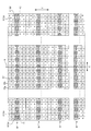
- FIG. 3 is an enlarged schematic view of a light receiving surface 50 shown in FIG. 2.
- FIG. 4 is a schematic plan view illustrating a pixel configuration of imaging pixels 60r, 60g, and 60b illustrated in FIG. 3.
- FIG. 4 is a schematic plan view showing a pixel configuration of left eccentric phase difference detection pixels 61Ggl and 61Gbl shown in FIG. 3.
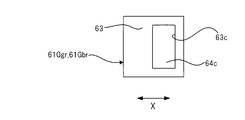
- FIG. 4 is a schematic plan view showing a pixel configuration of right eccentric phase difference detection pixels 61Ggr and 61Gbr shown in FIG. 3.
- FIG. 3 is a diagram illustrating a schematic configuration of a digital camera that is an embodiment of an imaging apparatus of the present invention.
- FIG. 2 is a schematic plan view showing a schematic configuration of an image sensor 5
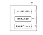
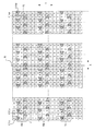
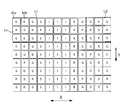
- FIG. 2 is a functional block diagram of a digital signal processing unit 17 in the digital camera shown in FIG. 1. It is an enlarged schematic diagram which shows the 1st modification of the light-receiving surface 50 shown in FIG. It is an enlarged schematic diagram which shows the 2nd modification of the light-receiving surface 50 shown in FIG. It is an enlarged schematic diagram which shows the 5th modification of the light-receiving surface 50 shown in FIG. It is an expansion schematic diagram which shows the 6th modification of the light-receiving surface 50 shown in FIG. It is a schematic diagram which shows the pixel arrangement pattern of an image pick-up element. It is a figure which shows the external appearance of the smart phone which is one Embodiment of an imaging device. It is a block diagram which shows the structure of the smart phone shown in FIG.
- FIG. 1 is a diagram showing a schematic configuration of a digital camera which is an embodiment of an imaging apparatus of the present invention.
- the imaging system of the digital camera shown in FIG. 1 includes an imaging optical system having an imaging lens 1 and a diaphragm 2, and an imaging element 5 such as a CCD image sensor or a CMOS image sensor.
- the imaging lens 1 includes at least a focus lens.
- This focus lens is a lens for adjusting the focal position of the imaging optical system, and is composed of a single lens or a plurality of lenses. The focus position is adjusted by moving the focus lens in the optical axis direction of the imaging optical system.
- the imaging device 5 has a configuration in which a plurality of imaging pixels and phase difference detection pixels that respectively receive a pair of light beams that have passed through different portions of the pupil region of the imaging optical system are arranged in a two-dimensional manner. Yes.
- the imaging element 5 can photoelectrically convert the optical image formed by the imaging lens 1 and output a captured image signal, and can output a pair of image signals corresponding to the pair of light beams.
- the system control unit 11 that performs overall control of the entire electric control system of the digital camera controls the lens driving unit 8 to adjust the position of the focus lens included in the imaging lens 1. Further, the system control unit 11 adjusts the exposure amount by controlling the aperture amount of the aperture 2 via the aperture drive unit 9.
- system control unit 11 drives the imaging device 5 via the imaging device driving unit 10 and outputs the subject image captured through the imaging lens 1 as a captured image signal.
- An instruction signal from the user is input to the system control unit 11 through the operation unit 14.
- the electric control system of the digital camera further includes an analog signal processing unit 6 that performs analog signal processing such as correlated double sampling processing connected to the output of the image sensor 5, and R (output from the analog signal processing unit 6).
- An analog-digital (A / D) conversion circuit 7 that converts a color signal of a red component, a color signal of a G (green) component, and a color signal of a B (blue) component into a digital signal.
- the analog signal processing unit 6 and the A / D conversion circuit 7 are controlled by the system control unit 11.
- the electric control system of the digital camera performs image processing on the main memory 16, the memory control unit 15 connected to the main memory 16, and the picked-up image signal obtained by picking up the image by the image pickup device 5 to obtain picked-up image data.
- a digital signal processing unit 17 that generates the image signal
- a focus detection unit 19 that calculates the defocus amount of the imaging lens 1 based on the phase difference between the pair of image signals output from the phase difference detection pixels of the imaging device 5, and attachment / detachment
- An external memory control unit 20 to which a free recording medium 21 is connected and a display control unit 22 to which a display unit 23 mounted on the back of the camera or the like is connected are provided.
- the memory control unit 15, the digital signal processing unit 17, the focus detection unit 19, the external memory control unit 20, and the display control unit 22 are mutually connected by a control bus 24 and a data bus 25, and commands from the system control unit 11. Controlled by.
- Each of the system control unit 11 and the digital signal processing unit 17 includes various processors that execute processing by executing a program, a RAM (Random Access Memory), and a ROM (Read Only Memory).
- the various processors can change the circuit configuration after manufacturing a CPU (Central Processing Unit), an FPGA (Field Programmable Gate Array), etc., which are general-purpose processors that execute various processes by executing programs. Includes a dedicated electrical circuit that is a processor having a circuit configuration designed specifically to execute a specific process such as a programmable logic device (Programmable Logic Device: PLD) or an ASIC (Application Specific Integrated Circuit). .
- a CPU Central Processing Unit
- FPGA Field Programmable Gate Array
- a dedicated electrical circuit that is a processor having a circuit configuration designed specifically to execute a specific process such as a programmable logic device (Programmable Logic Device: PLD) or an ASIC (Application Specific Integrated Circuit).
- the structures of these various processors are electric circuits in which circuit elements such as semiconductor elements are combined.
- Each of the system control unit 11 and the digital signal processing unit 17 may be configured by one of various processors, or a combination of two or more processors of the same type or different types (for example, a combination of a plurality of FPGAs or (Combination of CPU and FPGA).
- FIG. 2 is a schematic plan view showing a schematic configuration of the image sensor 5 mounted on the digital camera shown in FIG.
- a large number of pixels (not shown) arranged two-dimensionally in a row direction (left-right direction) X and a column direction (vertical direction) Y orthogonal to the row direction X are formed.
- a plurality of rectangular phase difference detection areas 53 are set at arbitrary region positions of the light receiving surface 50 (substantially the entire region in the light receiving surface 50 in the illustrated example).
- the phase difference detection area 53 is an area set so as to include the phase difference detection pixels on the light receiving surface 50 as a range corresponding to the subject to be focused.
- Each of the 35 phase difference detection areas 53 shown in FIG. 2 has a minimum size that can be set as the phase difference detection area 53, and a phase difference detection area having a size larger than the minimum size on the light receiving surface 50. Can also be set.
- a straight line N extending in the column direction Y shown in FIG. 2 indicates a virtual straight line that extends in the column direction Y through the intersection of the optical axis of the imaging optical system of the digital camera and the light receiving surface 50.
- the row direction X corresponds to “any direction” recited in the claims
- the column direction Y corresponds to “orthogonal direction” recited in the claims
- the left direction Corresponds to “one direction in the row direction X” recited in the claims
- the right direction corresponds to “the other direction in the row direction X” recited in the claims.
- the position of the straight line N in the row direction X corresponds to “arbitrary position” recited in the claims.
- FIG. 3 is an enlarged schematic view of the light receiving surface 50 shown in FIG.
- an imaging pixel 60 r (a block marked with “R” in the figure) that photoelectrically converts R light and outputs an R component signal (R signal), and photoelectrically converts G light.
- an imaging pixel 60g (a block with “G” in the figure) that outputs a G component signal (G signal) and an imaging pixel that photoelectrically converts B light and outputs a B component signal (B signal).
- Pixels 60b (blocks marked with “B” in the figure) are two-dimensionally arranged according to a Bayer array that is a regular pattern.
- a part of the arrangement position of the imaging pixels 60g based on the Bayer arrangement (position where the imaging pixels 60g should be arranged according to the Bayer arrangement). Further, a left eccentric phase difference detection pixel 61Ggl that photoelectrically converts G light and outputs a G signal is disposed.
- a part of the arrangement position of the imaging pixels 60b based on the Bayer arrangement position where the imaging pixels 60b should be arranged according to the Bayer arrangement.
- a right eccentric phase difference detection pixel 61Gbr that photoelectrically converts G light and outputs a G signal is disposed.
- a right eccentricity that photoelectrically converts G light and outputs a G signal to a part of the arrangement position of the imaging pixels 60g based on the Bayer array.
- a phase difference detection pixel 61Ggr is arranged.
- a phase difference detection pixel 61Gbl is arranged.
- FIG. 4 is a schematic plan view showing the pixel configuration of the imaging pixels 60r, 60g, and 60b shown in FIG.
- FIG. 5 is a schematic plan view showing the pixel configuration of the left eccentric phase difference detection pixels 61Ggl and 61Gbl shown in FIG.
- FIG. 6 is a schematic plan view showing the pixel configuration of the right eccentric phase difference detection pixels 61Ggr and 61Gbr shown in FIG.
- the imaging pixels 60r, 60g, and 60b have an opening 63a at a position where the light shielding film 63 provided on the photoelectric conversion unit (photodiode) overlaps substantially the entire photoelectric conversion unit.
- the photoelectric conversion portion that overlaps with the opening 63 a constitutes the photoelectric conversion region 64.
- the position of the center of the photoelectric conversion region 64 in the row direction X indicates the position of the photoelectric conversion region 64, and this position is a reference position.
- the imaging pixels 60r, 60g, and 60b are a pair of lights that have passed through different portions of the pupil region of the imaging lens 1 shown in FIG. 1 (light that has passed through the left side and light that has passed through the right side with respect to the main axis of the imaging lens 1). These are pixels that receive and photoelectrically convert both.
- the left eccentric phase difference detection pixels 61Ggl and 61Gbl are provided such that the center of the opening 63b of the light shielding film 63 provided on the photoelectric conversion portion is eccentric to the left with respect to the opening 63a in FIG.
- the photoelectric conversion portion overlapping the opening 63b constitutes a photoelectric conversion region 64b.
- the center of the photoelectric conversion region 64b in the row direction X indicates the position of the photoelectric conversion region 64b, and this position is eccentric to the left with respect to the position of the photoelectric conversion region 64.
- the left eccentric phase difference detection pixels 61Ggl and 61Gbl are pixels that receive one of the pair of lights and perform photoelectric conversion.
- the left eccentric phase difference detection pixels 61Ggl and 61Gbl constitute first phase difference detection pixels, respectively.
- the right eccentric phase difference detection pixels 61Ggr and 61Gbr are provided such that the center of the opening 63c of the light shielding film 63 provided on the photoelectric conversion unit is eccentric to the right with respect to the opening 63a in FIG.
- the photoelectric conversion portion overlapping the opening 63c constitutes a photoelectric conversion region 64c.
- the center of the photoelectric conversion region 64c in the row direction X indicates the position of the photoelectric conversion region 64c, and this position is eccentric to the right side with respect to the position of the photoelectric conversion region 64.
- the right eccentric phase difference detection pixels 61Ggr and 61Gbr are pixels that receive the other light of the pair of lights and perform photoelectric conversion.
- the right eccentric phase difference detection pixels 61Ggr and 61Gbr each constitute a second phase difference detection pixel.
- the imaging pixel 60r, the imaging pixel 60g, the imaging pixel 60b, the left eccentric phase difference detection pixels 61Ggl and 61Gbl, and the right eccentric phase difference detection pixel 61Ggr. , 61 Gbr a total of seven types of pixels are arranged two-dimensionally.
- the digital signal processing unit 17 of the digital camera shown in FIG. 1 performs a demosaic process on a captured image signal that is a set of output signals of all the pixels included in the image sensor 5, and each pixel of the image sensor 5.
- R signal, G signal, and B signal are generated in correspondence with the position of, and a luminance signal corresponding to the position of each pixel is generated by weighting and adding the R signal, G signal, and B signal. .
- the digital signal processing unit 17 obtains a luminance signal by weighting and adding the R signal, the G signal, and the B signal at a ratio of 3: 6: 1.
- the digital signal processing unit 17 generates a color difference signal using the luminance signal, the R signal, the G signal, and the B signal.
- a pixel signal composed of a luminance signal and a color difference signal is generated in correspondence with the position of each pixel of the image sensor 5, and captured image data is configured by a set of the pixel signals.
- a pixel that outputs an R signal (imaging pixel 60r), a pixel that outputs a G signal (imaging pixel 60g, left eccentric phase difference detection pixel) 61Ggl, 61Gbl, right eccentricity phase difference detection pixel 61Ggr, 61Gbr), and a pixel that outputs a B signal (imaging pixel 60b), a pixel that outputs a G signal contributes most to obtain a luminance signal
- a second pixel that outputs a signal of a component (first color component), a pixel that outputs a B signal, and a pixel that outputs an R signal each outputs a color signal other than the first color component. It becomes.
- pixels that output the G signal and pixels that output the B signal alternate in the row direction X.
- a part of the large number of GB pixel rows arranged in the column is a phase difference detection pixel row M.
- the phase difference detection pixel rows M are arranged on the light receiving surface 50 in the column direction Y, for example, at equal intervals (in the example of FIG. 3, one pixel is arranged in six pixel rows).
- the left eccentric phase difference detection pixel 61Ggl is arranged at the position where the pixel that outputs the G signal in the Bayer arrangement is to be arranged, and the B signal in the Bayer arrangement
- the right eccentric phase difference detection pixel 61Gbr is arranged at a position where a pixel for outputting the signal is to be arranged.
- the right eccentric phase difference detection pixel 61Ggr is arranged at the position where the pixel outputting the G signal in the Bayer arrangement is to be arranged.
- a left eccentric phase difference detection pixel 61Gbl is disposed at a position where a pixel that outputs a B signal is to be disposed.
- each phase difference detection pixel row M includes a plurality of first pairs P1 of the left eccentric phase difference detection pixel 61Ggl and the right eccentric phase difference detection pixel 61Gbr arranged on the left side of the straight line N, and straight lines.
- a plurality of pairs arranged in the row direction X including a right eccentric phase difference detection pixel 61Ggr and a plurality of second pairs P2 of left eccentric phase difference detection pixels 61Gbl arranged on the right side of N. Yes.
- the phase difference detection pixel rows M constitute a pair row.
- each phase difference detection pixel row M the plurality of first pairs P1 are arranged on the left side of the straight line N, and the plurality of second pairs P2 are arranged on the right side of the straight line N.
- the focus detection unit 19 shown in FIG. 1 divides the pupil region of the imaging optical system into two in the row direction X based on the output signal of the phase difference detection pixels included in the phase difference detection area 53 selected by the user of the digital camera. The phase difference between a pair of image signals imaged through each divided region obtained in this way is calculated.
- the focus detection unit 19 detects the left eccentric phase difference detection pixel 61Ggl and the right eccentric phase difference detection that constitute the first pair P1 of each phase difference detection pixel row M included in the selected phase difference detection area 53.
- a phase difference is calculated by performing a correlation operation between the output signal groups of the pixels 61Gbr, and a defocus amount is calculated based on the phase difference.
- the focus detection unit 19 outputs each of the output signal groups of the right eccentric phase difference detection pixel 61Ggr and the left eccentric phase difference detection pixel 61Gbl constituting the second pair P2 included in the selected phase difference detection area 53.
- a phase difference is calculated by performing a correlation calculation between them, and a defocus amount is calculated based on the phase difference.
- the system control unit 11 illustrated in FIG. 1 performs focus adjustment by controlling the position of the focus lens included in the imaging lens 1 based on the defocus amount calculated by the focus detection unit 19.
- the system control unit 11 causes the imaging device 5 to perform imaging, and the captured image signal output from the imaging device 5 by this imaging is a digital signal. It is taken into the processing unit 17.
- the digital signal processing unit 17 processes the captured image signal to generate captured image data. This image processing includes demosaic processing, gamma correction processing, white balance adjustment processing, and the like.
- the digital signal processing unit 17 constitutes an image processing unit that generates captured image data based on signals output from the pixels of the image sensor 5.
- FIG. 7 is a functional block diagram of the digital signal processing unit 17 in the digital camera shown in FIG.
- the digital signal processing unit 17 includes a gain correction processing unit 171, an interpolation correction processing unit 172, and a captured image data generation unit 173.
- the gain correction processing unit 171, the interpolation correction processing unit 172, and the captured image data generation unit 173 are functional blocks formed by a processor included in the digital signal processing unit 17 executing a program.
- the gain correction processing unit 171 and the interpolation correction processing unit 172 constitute a correction unit.
- the gain correction processing unit 171 multiplies the output signal of each of the left eccentric phase difference detection pixel Ggl and the right eccentric phase difference detection pixel Ggr by a gain to obtain the left eccentric phase difference detection pixel Ggl and the right eccentric phase difference detection. A pixel signal corresponding to each position of the pixel Ggr is generated.
- the interpolation correction processing unit 172 outputs pixel signals corresponding to the positions of the left eccentric phase difference detection pixel Gbl and the right eccentric phase difference detection pixel Gbr, to the left eccentric phase difference detection pixel Gbl and the right eccentric phase difference detection. Interpolation is generated based on the output signal (B signal) of the imaging pixel 60b around each of the pixels Gbr.
- the interpolation correction processing unit 172 calculates the average of the output signals of each of the two imaging pixels 60b that are close to the top and bottom of the left eccentric phase difference detection pixel Gbl, and uses this average as the left eccentric phase difference detection It is assumed that the pixel signal corresponds to the position of the pixel Gbl.
- the captured image data generation unit 173 includes the output signal of the imaging pixel 60r, the output signal of the imaging pixel 60g, the output signal of the imaging pixel 60b, the left eccentric phase difference detection pixel Ggl, Signals corrected by the gain correction processing unit 171 of each output signal of the right eccentric phase difference detection pixel Ggr, the left eccentric phase difference detection pixel Gbl generated by interpolation by the interpolation correction processing unit 172, and the right eccentric phase difference detection Based on the pixel signal corresponding to each position of the pixel Gbr, the captured image data including the luminance signal and the color difference signal is generated.
- the generated captured image data can be recorded on the recording medium 21 via the external memory control unit 20 or displayed as an image on the display unit 23 via the display control unit 22, for example.
- the left eccentric phase difference detection pixel 61Ggl is arranged in the left region of the light receiving surface 50 with the straight line N as a boundary, and the right side of the light receiving surface 50
- the right eccentric phase difference detection pixel 61Ggr is arranged in the area.
- the sensitivity characteristics of the left eccentric phase difference detection pixel 61Ggl and the right eccentric phase difference detection pixel 61Ggr having the same distance from the straight line N can be made the same.
- the level of the output signal of the phase difference detection pixel that outputs the G signal on the right or left side of the straight line N can be prevented from being relatively lowered.
- the output signals of the left eccentric phase difference detection pixel 61Ggl and the right eccentric phase difference detection pixel 61Ggr can be returned to levels that can be used as pixel signals with an appropriate gain. By eliminating the need to increase the gain, noise can be suppressed and the captured image quality can be improved.
- each output signal of the left eccentric phase difference detection pixel 61Ggl and the right eccentric phase difference detection pixel 61Ggr is a G signal, and has the largest contribution to the luminance signal. For this reason, the gain of the output signal can be corrected, so that the captured image quality can be improved.
- pixel signals corresponding to the positions of the left eccentric phase difference detection pixel 61Gbl and the right eccentric phase difference detection pixel 61Gbr are generated by interpolation based on the B signal that is the output signal of the imaging pixel 60b.
- the B signal has the lowest contribution to the luminance signal among the R signal, the G signal, and the B signal. For this reason, it is possible to minimize the influence on the captured image quality due to the interpolation generation of the pixel signals corresponding to the positions of the left eccentric phase difference detection pixel 61Gbl and the right eccentric phase difference detection pixel 61Gbr.
- the phase difference detection pixels are arranged at a part of the positions where the imaging pixels 60g and the imaging pixels 60b are to be arranged according to the Bayer array.
- the present invention is not limited to this.
- phase difference detection pixels are arranged at positions where the imaging pixels 60g and the imaging pixels 60r should be arranged according to the Bayer array.
- the configuration may be a phase difference detection pixel row M.
- the left eccentric phase difference detection pixel 61Ggl is arranged at the position where the imaging pixel 60g is to be arranged, and the imaging pixel 60r is arranged.
- the right eccentric phase difference detection pixel 61Gbr is arranged at the position to be.
- each phase difference detection pixel row M on the right side of the straight line N, the right eccentric phase difference detection pixel 61Ggr is arranged at the position where the imaging pixel 60g should be arranged, and the imaging pixel 60r should be arranged.
- the left eccentric phase difference detection pixel 61Gbl is disposed at the position.
- the boundary between the portion where the first pair P1 is aligned in the row direction X and the portion where the second pair P2 is aligned in the row direction X is determined by the position of the straight line N.
- the position of this boundary is not limited to the position of the straight line N.
- the first pair P1 of each phase difference detection pixel row M is aligned with the straight line parallel to the straight line N, and the straight line is shifted to the right or left by, for example, two pixels from the straight line N.
- the boundary of the portion where the second pair P2 is arranged may be configured.
- phase difference detection areas 53 that are parallel to the straight line N and that are in the center in the row direction X of FIG. 2 and the phase difference detection areas 53 that are adjacent to each other in the row direction X.
- the boundary between the portion where the first pairs P1 of the phase difference detection pixel rows M are arranged and the portion where the second pairs P2 are arranged may be configured by a straight line passing through the region.
- the position in the row direction X of the boundary in the phase difference detection pixel row M is arbitrary, but the position of the boundary is preferably in the vicinity of the position of the straight line N.
- the vicinity of the straight line N means that the picked-up image quality is as close as possible to the straight line N.
- the position in the row direction X of the straight line N is a few pixels to several hundred pixels away from this position in the row direction X.
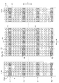
- FIG. 8 is an enlarged schematic view showing a first modification of the light receiving surface 50 shown in FIG.
- the imaging device 5 of the first modification shown in FIG. 8 replaces the phase difference detection pixel row M with 2 of the first phase difference detection pixel row M1 and the second phase difference detection pixel row M2. Two patterns of phase difference detection pixel rows are provided. Other configurations are the same as those shown in FIG.
- the boundary between the portion where the first pair P1 is arranged and the portion where the second pair P2 is arranged is parallel to the straight line N and rightward with respect to the straight line N Is formed by a straight line N1 at a position shifted by two pixels.
- the distance between the straight line N1 and the straight line N is two pixels, but this distance may be a distance corresponding to an arbitrary number of pixels.
- the first phase difference detection pixel row M1 forms a first pair row.
- the boundary between the portion where the first pair P1 is arranged and the portion where the second pair P2 is arranged is parallel to the straight line N and leftward with respect to the straight line N Is formed by a straight line N2 at a position shifted by two pixels.
- the distance between the straight line N2 and the straight line N is two pixels, but this distance may be a distance corresponding to an arbitrary number of pixels.
- the second phase difference detection pixel row M2 constitutes a second pair row.
- a plurality of phase difference detection pixel rows including a first phase difference detection pixel row M1 and a second phase difference detection pixel row M2 are arranged in the column direction on the light receiving surface 50 of the image sensor 5 of the first modification. They are alternately arranged in Y with periodicity.
- the imaging element 5 includes the first phase difference detection pixel in which the position of the boundary between the portion where the first pair P1 is arranged and the portion where the second pair P2 is arranged is different.
- each of the five phase difference detection areas 53 at the center in the row direction X of FIG. 2 and the phase difference detection areas 53 on both sides of the respective row directions X are arranged.
- each phase difference detection area 53 shown in FIG. 2 has at least one phase difference detection pixel row in which the boundary exists outside. Will be included.
- phase difference detection pixel rows that do not cross the boundary always exist in each phase difference detection area 53, so that the phase difference of the subject image captured in each phase difference detection area 53 can be accurately calculated. Can do. As a result, the focusing accuracy of the digital camera can be improved.
- the size of the phase difference detection area set on the light receiving surface 50 can be made larger than that of the phase difference detection area 53 shown in FIG.
- each of the phase difference detection areas that can be set has a phase difference detection pixel on the outside.
- a configuration including at least one row is preferable.
- the above-described boundary is provided outside each of the settable phase difference detection areas by adopting a configuration that satisfies the following conditions (1) and (2). Are included in at least one phase difference detection pixel row.
- Condition (1) The distance between the straight line N1 and the straight line N2 in the row direction X is larger than the width of the maximum size of the phase difference detection area in the row direction X.
- Condition (2) The distance between the first phase difference detection pixel row M1 and the second phase difference detection pixel row M2 adjacent thereto is smaller than the width in the column direction Y of the minimum size of the phase difference detection area.
- the phase difference of the subject image captured by the set phase difference detection area can be calculated with high accuracy. And focusing accuracy can be improved.
- the interpolation performed by the digital signal processing unit 17 is performed.
- the algorithm for the correction process can be simplified.
- FIG. 9 is an enlarged schematic view showing a second modification of the light receiving surface 50 shown in FIG.
- the imaging device 5 of the second modification shown in FIG. 9 includes N first phase difference detection pixel rows M1 and second phase difference detection pixel rows M2 with N being a natural number of 2 or more ( 9 differs from the image sensor 5 of the first modified example in that it is alternately arranged with periodicity in the column direction Y every two) in the example of FIG. Other configurations are the same as those of the image sensor 5 of the first modification.
- each of the five phase difference detection areas 53 at the center in the row direction X of FIG. 2 and the phase difference detection areas 53 on both sides of the respective row directions X are arranged. Since there is at least one of the straight line N1 and the straight line N2 in the area between them, each of the phase difference detection areas 53 shown in FIG. 2 includes at least one phase difference detection pixel row in which the above boundary exists. It will be.
- phase difference detection pixel row that does not cross the boundary in each phase difference detection area 53
- the phase difference of the subject image captured in each phase difference detection area 53 can be accurately calculated. .
- the focusing accuracy of the digital camera can be improved.
- the boundary is outside the settable phase difference detection area. Is preferably configured to include at least one phase difference detection pixel row.
- the above-described boundary is located outside each of all the settable phase difference detection areas by adopting a configuration that satisfies the following conditions (3) and (4).
- Condition (3) The distance between the straight line N1 and the straight line N2 in the row direction X is larger than the width of the maximum size of the phase difference detection area in the row direction X.
- Condition (4) A value obtained by multiplying the distance between adjacent phase difference detection pixel rows in the column direction Y by N is smaller than the width in the column direction Y of the minimum size of the phase difference detection area.
- the phase difference of the subject image captured by the set phase difference detection area can be calculated with high accuracy. And focusing accuracy can be improved.
- another first phase difference detection pixel row M1 always exists next to the first phase difference detection pixel row M1 in the column direction Y.
- Another second phase difference detection pixel row M2 always exists next to the phase difference detection pixel row M2 in the column direction Y.
- the defect correction of this pixel is performed with an adjacent pixel having the same configuration as this pixel. This can be done using the output signal of the pixel. Therefore, the accuracy of defect correction when there are defective pixels can be improved.
- the interpolation performed by the digital signal processing unit 17 is performed.
- the algorithm for the correction process can be simplified.
- the first phase difference detection pixel row M1 and the second phase difference detection pixel row M2 are periodically arranged in the column direction Y.
- the first phase difference detection pixel row M1 and the second phase difference detection pixel row M2 may be randomly arranged in the column direction Y. Even with such a configuration, the quality of the captured image can be improved.
- the imaging element 5 may have a configuration in which three or more phase difference detection pixel rows having different boundary positions are formed on the light receiving surface 50. Even with such a configuration, the quality of the captured image can be improved.
- the interpolation correction algorithm can be simplified by periodically arranging three or more phase difference detection pixel rows in the column direction Y. Moreover, focusing accuracy can be improved by setting it as the structure which satisfy
- the first pair P1 and the second pair P2 are each configured by two phase difference detection pixels having the same position in the column direction Y, but two phase difference detections having different positions in the column direction Y are used.
- the first pair P1 and the second pair P2 may be configured by the use pixels.
- FIG. 10 is an enlarged schematic view showing a fifth modification of the light receiving surface 50 shown in FIG.
- the imaging element 5 shown in FIG. 10 has a left eccentric phase difference at a position where the imaging pixel 60g is to be arranged on the left side of the straight line N of the upper pixel row of the two GB pixel rows adjacent in the column direction Y.
- a detection pixel 61Ggl is arranged, and a left eccentric phase difference detection pixel 61Gbl is arranged at a position where the imaging pixel 60b is to be arranged on the right side of the straight line N of the pixel row.
- a right eccentric phase difference detection pixel at a position where the imaging pixel 60b is to be arranged on the left side of the straight line N of the lower pixel row of the two GB pixel rows.
- 61 Gbr is arranged, and on the right side of the straight line N of this pixel row, a right eccentric phase difference detection pixel 61 Ggr is arranged at a position where the imaging pixel 60 g is to be arranged.
- the for-use pixel 61Gbr constitutes the first pair P1.
- the detection pixel 61Gbl forms a second pair P2.
- a plurality of first pairs P1 arranged in the row direction X and a plurality of second pairs P2 arranged in the row direction X constitute a phase difference detection pixel row Ma.
- the image sensor 5 may have a configuration in which a large number of pixels are arranged according to a pattern other than the Bayer array.
- FIG. 11 is an enlarged schematic view showing a sixth modification of the light receiving surface 50 shown in FIG.
- the ratio of the number of pixels that photoelectrically convert R light, the number of pixels that photoelectrically convert B light, and the number of pixels that photoelectrically convert G light is 1: 1. They are arranged according to a pattern of 2.5.
- the unit U1 including the imaging pixels 60r, 60g, and 60b and the unit U2 in which the positions of the imaging pixel 60r and the imaging pixel 60b are replaced in the unit U1 are checkered. It is an arranged pattern.
- the imaging pixels 60g are arranged at the four corners and the center.
- an imaging pixel 60r is arranged on both sides in the row direction X of the central imaging pixel 60g
- an imaging pixel 60b is arranged on both sides in the column direction Y of the central imaging pixel 60g.
- the configuration and effects of the pixel array shown in FIG. 12 are described in detail in International Publication No. WO13 / 168493, and therefore description thereof is omitted.
- the imaging element 5 of the sixth modified example shown in FIG. 11 is for detecting the left eccentric phase difference at a part of the position where the imaging pixel 60g on the left side of the straight line N is to be arranged in the pixel array shown in FIG.
- the pixel 61Ggl is arranged, and the right eccentric phase difference detection pixel 61Ggr is arranged at a part of the position where the imaging pixel 60g on the right side of the straight line N is to be arranged.
- the imaging element 5 shown in FIG. 11 has a right eccentric phase difference detection pixel 61Gbr at a part of a position where the imaging pixels 60b and 60r on the left side of the straight line N are to be arranged in the pixel array shown in FIG. Is arranged, and the left eccentric phase difference detection pixel 61Gbl is arranged at a part of the position where the imaging pixels 60b and 60r on the right side of the straight line N are to be arranged.
- the first pair P1 is configured by the left eccentric phase difference detection pixel 61Ggl and the right eccentric phase difference detection pixel 61Gbr which is obliquely downward to the right of the left eccentric phase difference detection pixel 61Ggl.
- the second pair P2 is configured by the right eccentric phase difference detection pixel 61Ggr and the left eccentric phase difference detection pixel 61Gbl which is obliquely downward to the right of the right eccentric phase difference detection pixel 61Ggr.
- the plurality of first pairs P1 and the plurality of second pairs P2 constitute a phase difference detection pixel row Mb.
- the same effect as the image sensor 5 shown in FIG. 3 can be obtained. Also in the configuration shown in FIG. 11, the configurations described in the first to fourth modifications can be applied.
- FIG. 13 shows an appearance of a smartphone 200 that is an embodiment of the imaging apparatus of the present invention.
- a smartphone 200 illustrated in FIG. 13 includes a flat housing 201, and a display input in which a display panel 202 as a display unit and an operation panel 203 as an input unit are integrated on one surface of the housing 201. Part 204 is provided.
- Such a casing 201 includes a speaker 205, a microphone 206, an operation unit 207, and a camera unit 208.
- the configuration of the housing 201 is not limited to this, and for example, a configuration in which the display unit and the input unit are independent may be employed, or a configuration having a folding structure and a slide mechanism may be employed.
- FIG. 14 is a block diagram showing a configuration of the smartphone 200 shown in FIG.
- the main components of the smartphone include a wireless communication unit 210, a display input unit 204, a call unit 211, an operation unit 207, a camera unit 208, a storage unit 212, and an external input / output unit. 213, a GPS (Global Positioning System) receiving unit 214, a motion sensor unit 215, a power supply unit 216, and a main control unit 220.
- a wireless communication function for performing mobile wireless communication via a base station device BS (not shown) and a mobile communication network NW (not shown) is provided.
- the wireless communication unit 210 performs wireless communication with the base station apparatus BS accommodated in the mobile communication network NW according to an instruction from the main control unit 220. Using this wireless communication, transmission and reception of various file data such as audio data and image data, e-mail data, and reception of Web data and streaming data are performed.
- the display input unit 204 controls the main control unit 220 to display images (still images and moving images), character information, and the like to visually transmit information to the user and to detect user operations on the displayed information.
- a so-called touch panel which includes a display panel 202 and an operation panel 203.
- the display panel 202 uses an LCD (Liquid Crystal Display), an OELD (Organic Electro-Luminescence Display), or the like as a display device.
- LCD Liquid Crystal Display
- OELD Organic Electro-Luminescence Display
- the operation panel 203 is a device that is placed so that an image displayed on the display surface of the display panel 202 is visible and detects one or more coordinates operated by a user's finger or stylus.
- a detection signal generated due to the operation is output to the main control unit 220.
- the main control unit 220 detects an operation position (coordinates) on the display panel 202 based on the received detection signal.
- the display panel 202 and the operation panel 203 of the smartphone 200 exemplified as an embodiment of the imaging apparatus of the present invention integrally form a display input unit 204.
- the arrangement 203 covers the display panel 202 completely.
- the operation panel 203 may have a function of detecting a user operation even in an area outside the display panel 202.
- the operation panel 203 includes a detection area (hereinafter referred to as a display area) for an overlapping portion that overlaps the display panel 202 and a detection area (hereinafter, a non-display area) for an outer edge portion that does not overlap the other display panel 202. May be included).
- the size of the display area and the size of the display panel 202 may be completely matched, it is not always necessary to match the two.
- the operation panel 203 may include two sensitive areas of the outer edge portion and the other inner portion.
- the width of the outer edge portion is appropriately designed according to the size of the housing 201 and the like.
- examples of the position detection method employed in the operation panel 203 include a matrix switch method, a resistance film method, a surface acoustic wave method, an infrared method, an electromagnetic induction method, a capacitance method, and the like. You can also
- the call unit 211 includes a speaker 205 and a microphone 206, converts user's voice input through the microphone 206 into voice data that can be processed by the main control unit 220, and outputs the voice data to the main control unit 220. 210 or the audio data received by the external input / output unit 213 is decoded and output from the speaker 205.
- the speaker 205 can be mounted on the same surface as the surface on which the display input unit 204 is provided, and the microphone 206 can be mounted on the side surface of the housing 201.
- the operation unit 207 is a hardware key using a key switch or the like, and receives an instruction from the user.
- the operation unit 207 is mounted on the side surface of the housing 201 of the smartphone 200 and is turned on when pressed with a finger or the like, and turned off when the finger is released with a restoring force such as a spring. It is a push button type switch.
- the storage unit 212 includes a control program and control data of the main control unit 220, application software, address data that associates the name and telephone number of a communication partner, transmitted / received e-mail data, Web data downloaded by Web browsing, The downloaded content data is stored, and streaming data and the like are temporarily stored.
- the storage unit 212 includes an internal storage unit 217 built in the smartphone and an external storage unit 218 having an external memory slot that can be freely attached and detached.
- Each of the internal storage unit 217 and the external storage unit 218 constituting the storage unit 212 includes a flash memory type (hard memory type), a hard disk type (hard disk type), a multimedia card micro type (multimedia card micro type), This is realized using a storage medium such as a card type memory (for example, MicroSD (registered trademark) memory), a RAM (Random Access Memory), a ROM (Read Only Memory), or the like.
- the external input / output unit 213 serves as an interface with all external devices connected to the smartphone 200, and communicates with other external devices (for example, universal serial bus (USB), IEEE 1394, etc.) or a network.
- external devices for example, universal serial bus (USB), IEEE 1394, etc.
- a network for example, Internet, wireless LAN, Bluetooth (registered trademark), RFID (Radio Frequency Identification), Infrared Data Association (IrDA) (registered trademark), UWB (Ultra Wideband) (registered trademark) ZigBee) (registered trademark, etc.) for direct or indirect connection.
- an external device connected to the smartphone 200 for example, a wired / wireless headset, a wired / wireless external charger, a wired / wireless data port, a memory card (Memory card) connected via a card socket, or a SIM (Subscriber).
- Identity Module Card / UIM (User Identity Module Card) card external audio / video equipment connected via audio / video I / O (Input / Output) terminal, external audio / video equipment connected wirelessly, yes / no
- the external input / output unit 213 transmits data received from such an external device to each component inside the smartphone 200, or allows the data inside the smartphone 200 to be transmitted to the external device. Can do.
- the GPS receiving unit 214 receives GPS signals transmitted from the GPS satellites ST1 to STn in accordance with instructions from the main control unit 220, executes a positioning calculation process based on the received plurality of GPS signals, A position consisting of longitude and altitude is detected.
- the GPS reception unit 214 can acquire position information from the wireless communication unit 210 or the external input / output unit 213 (for example, a wireless LAN), the GPS reception unit 214 can also detect the position using the position information.
- the motion sensor unit 215 includes, for example, a three-axis acceleration sensor, and detects the physical movement of the smartphone 200 in accordance with an instruction from the main control unit 220. By detecting the physical movement of the smartphone 200, the moving direction and acceleration of the smartphone 200 are detected. The detection result is output to the main control unit 220.
- the power supply unit 216 supplies power stored in a battery (not shown) to each unit of the smartphone 200 in accordance with an instruction from the main control unit 220.
- the main control unit 220 includes a microprocessor, operates according to a control program and control data stored in the storage unit 212, and controls each unit of the smartphone 200 in an integrated manner.
- the main control unit 220 includes a mobile communication control function that controls each unit of the communication system and an application processing function in order to perform voice communication and data communication through the wireless communication unit 210.
- the application processing function is realized by the main control unit 220 operating according to the application software stored in the storage unit 212.
- Examples of the application processing function include an infrared communication function for controlling the external input / output unit 213 to perform data communication with the opposite device, an e-mail function for transmitting / receiving e-mails, and a web browsing function for browsing web pages. .
- the main control unit 220 has an image processing function such as displaying video on the display input unit 204 based on image data (still image or moving image data) such as received data or downloaded streaming data.
- the image processing function is a function in which the main control unit 220 decodes the image data, performs image processing on the decoding result, and displays an image on the display input unit 204.
- the main control unit 220 executes display control for the display panel 202 and operation detection control for detecting a user operation through the operation unit 207 and the operation panel 203. By executing the display control, the main control unit 220 displays an icon for starting application software, a software key such as a scroll bar, or a window for creating an e-mail.
- scroll bar refers to a software key for accepting an instruction to move the display portion of a large image that does not fit in the display area of the display panel 202.
- the main control unit 220 detects a user operation through the operation unit 207 or accepts an operation on the icon or an input of a character string in the input field of the window through the operation panel 203. Or a display image scroll request through a scroll bar.
- the main control unit 220 causes the operation position with respect to the operation panel 203 to overlap with the display panel 202 (display area) or other outer edge part (non-display area) that does not overlap with the display panel 202.
- a touch panel control function for controlling the sensitive area of the operation panel 203 and the display position of the software key.
- the main control unit 220 can also detect a gesture operation on the operation panel 203 and execute a preset function in accordance with the detected gesture operation.
- Gesture operation is not a conventional simple touch operation, but an operation that draws a trajectory with a finger or the like, designates a plurality of positions at the same time, or combines these to draw a trajectory for at least one of a plurality of positions. means.
- the camera unit 208 includes configurations other than the external memory control unit 20, the recording medium 21, the display control unit 22, the display unit 23, and the operation unit 14 in the digital camera shown in FIG.
- the captured image data generated by the camera unit 208 can be recorded in the storage unit 212 or output through the external input / output unit 213 or the wireless communication unit 210.
- the camera unit 208 is mounted on the same surface as the display input unit 204, but the mounting position of the camera unit 208 is not limited thereto, and may be mounted on the back surface of the display input unit 204. .
- the camera unit 208 can be used for various functions of the smartphone 200.
- an image acquired by the camera unit 208 can be displayed on the display panel 202, or the image of the camera unit 208 can be used as one of operation inputs of the operation panel 203.
- the position can also be detected with reference to an image from the camera unit 208.
- the optical axis direction of the camera unit 208 of the smartphone 200 is determined without using the triaxial acceleration sensor or in combination with the triaxial acceleration sensor. It is also possible to determine the current usage environment.
- the image from the camera unit 208 can also be used in the application software.
- the position information acquired by the GPS receiver 214 to the image data of the still image or the moving image, the voice information acquired by the microphone 206 (the text information may be converted into voice information by the main control unit or the like), Posture information and the like acquired by the motion sensor unit 215 can be added and recorded in the storage unit 212, or can be output through the external input / output unit 213 and the wireless communication unit 210.
- the digital signal processing unit 17 illustrated in FIGS. 1 and 5 performs the above-described processing, thereby enabling high-quality imaging.
- a white pixel that photoelectrically converts white light in addition to a pixel that outputs an R signal, a pixel that outputs a G signal, and a pixel that outputs a B signal, a white pixel that photoelectrically converts white light (for example, The present invention can also be applied to a pixel having no color filter.
- the phase detection pixels are arranged at the positions where the white pixels are to be arranged and the positions where the pixels outputting the R signal or the pixels outputting the B signal are arranged.
- the imaging device 5 of the above-described embodiment and each modification example is assumed to perform photoelectric conversion by splitting three colors of light, but the number of colors that can be split is the color that makes the maximum contribution to the luminance signal.
- the present invention can be applied even if two colors are included.
- the left eccentric phase difference detection pixel 61Ggl, the right eccentric phase difference detection pixel 61Ggr, the left eccentric phase difference detection pixel 61Gbl, and the right eccentric phase difference detection The color of light photoelectrically converted by each pixel 61Gbr is determined by the degree of contribution of the color to the luminance signal.
- the luminance signal is maximized with the ratio of the R signal among the R signal, the G signal, and the B signal generated corresponding to each pixel. It is possible to generate.
- the left eccentric phase difference detection pixel 61Ggl, the right eccentric phase difference detection pixel 61Ggr, the left eccentric phase difference detection pixel 61Gbl, and the right eccentric phase difference detection pixel 61Gbr each photoelectrically convert R light. Pixel.
- the left eccentric phase difference detection pixel 61Ggl is arranged at a part of the position where the imaging pixel 60r on the left side of the straight line N or the straight lines N1 and N2 is arranged, and on the right side of the straight line N or the straight lines N1 and N2.
- the right eccentric phase difference detection pixel 61Ggr is disposed at a part of the position where the imaging pixel 60r is to be disposed.
- the right eccentric phase difference detection pixel 61Gbr is arranged at a part of the position where the imaging pixel 60g or the imaging pixel 60b on the left side of the straight line N or the straight lines N1 and N2, and the straight line N or the straight line N1,
- the left eccentric phase difference detection pixel 61Gbl is arranged at a part of the position where the imaging pixel 60g or the imaging pixel 60b on the right side of N2 is to be arranged.
- the R signal having the maximum contribution to the luminance signal among the output signals of the phase difference detection pixels can be returned to a level usable as a pixel signal by gain correction. Quality can be improved.
- An imaging device having a plurality of pixels that photoelectrically convert light of different colors and having a light receiving surface in which the plurality of pixels are two-dimensionally arranged according to a regular pattern, wherein the plurality of pixels Includes a first pixel that outputs a signal of a first color component that contributes most to obtain a luminance signal, and a second pixel that outputs a signal of a color component other than the first color component,
- the first pixel includes a first imaging pixel having a photoelectric conversion region at a reference position and a first position having a photoelectric conversion region at a position decentered in one of arbitrary directions with respect to the reference position.
- the first phase difference detection pixel arranged at the arrangement position of the first pixel based on the pattern and the second arrangement arranged at the arrangement position of the second pixel based on the pattern A plurality of first pairs of phase difference detection pixels, the second phase difference detection pixels arranged at the arrangement positions of the first pixels based on the pattern, and the second pairs based on the pattern.
- a plurality of second pairs of the first phase difference detection pixels arranged at the arrangement position of the pixels, and a pair row composed of pairs arranged in the arbitrary direction is formed, and The plurality of first pairs included in the pair row are arranged on the one direction side from an arbitrary position in the arbitrary direction of the pair row, and the plurality of second pairs included in the pair row Pair in any direction above the pair row That the arbitrary image pickup element disposed in the direction of the other than the position.
- the imaging device according to any one of (1) to (8), and an image processing unit that generates captured image data based on signals output from the plurality of pixels of the imaging device. Imaging device.
- a pixel signal corresponding to the position of the pixel is generated by interpolation based on the output signal of the second imaging pixel around the first phase difference detection pixel, and the second pixel based on the pattern is generated.
- the second phase difference arranged at the arrangement position A correction unit that interpolates and generates a pixel signal corresponding to the position of the output pixel based on an output signal of the second imaging pixel around the second phase difference detection pixel; and the first imaging Captured image data for generating the captured image data composed of a luminance signal and a color difference signal based on the output signal of the pixel for pixels, the output signal of the second imaging pixel, and the pixel signal generated by the correction unit
- An imaging device comprising: a generation unit.
- An imaging device comprising: the imaging device according to any one of (1) to (8); and a processor that generates captured image data based on signals output from the plurality of pixels of the imaging device. .
- a pixel signal corresponding to the position is generated by interpolation based on the output signal of the second imaging pixel around the first phase difference detection pixel, and the arrangement position of the second pixel based on the pattern
- the second phase arranged in A pixel signal corresponding to the position of the detection pixel is generated by interpolation based on the output signal of the second imaging pixel around the second phase difference detection pixel, and the first imaging pixel
- an image pickup device capable of improving the picked-up image quality by enabling the use of gain correction as a correction method of the output signal of the phase difference detection pixel that makes the maximum contribution to the luminance signal, and
- An imaging device including an imaging element can be provided.
Landscapes
- Engineering & Computer Science (AREA)
- Multimedia (AREA)
- Signal Processing (AREA)
- Physics & Mathematics (AREA)
- General Physics & Mathematics (AREA)
- Optics & Photonics (AREA)
- Spectroscopy & Molecular Physics (AREA)
- Studio Devices (AREA)
- Automatic Focus Adjustment (AREA)
- Focusing (AREA)
- Transforming Light Signals Into Electric Signals (AREA)
- Color Television Image Signal Generators (AREA)
Abstract
輝度信号への寄与度が最大となる位相差検出用画素の出力信号の補正方法としてゲイン補正の採用を可能にして撮像画像品質を向上させることのできる撮像素子と、この撮像素子を備える撮像装置を提供する。撮像素子5の受光面50には複数の位相差検出用画素行Mが配列されている。位相差検出用画素行Mは、直線Nよりも左側の撮像用画素60gが配置されるべき位置に左偏心位相差検出用画素61Gglが配置され、直線Nよりも右側の撮像用画素60gが配置されるべき位置に右偏心位相差検出用画素61Ggrが配置され、直線Nよりも左側の撮像用画素60bが配置されるべき位置に右偏心位相差検出用画素61Gbrが配置され、直線Nよりも右側の撮像用画素60bが配置されるべき位置に左偏心位相差検出用画素61Gblが配置された構成である。
Description
本発明は、撮像素子及び撮像装置に関する。
CCD(Charge Coupled Device)イメージセンサ又はCMOS(Complementary Metal Oxide Semiconductor)イメージセンサ等の撮像素子の高解像度化に伴い、デジタルスチルカメラ、デジタルビデオカメラ、又は、スマートフォンを含む携帯電話機等の撮像機能を有する情報機器の需要が急増している。なお、以上のような撮像機能を有する情報機器を撮像装置と称する。
これら撮像装置では、主要な被写体に焦点を合わせる合焦制御方法として、位相差AF(Auto Forcus)方式(特許文献1、2参照)が採用されている。
位相差AF方式により合焦制御を行う撮像装置に搭載される撮像素子には、例えば、光電変換領域が互いに逆方向に偏心した位相差検出用画素のペアを受光面の全面に離散的に設けたものが使用される(特許文献1、2参照)。
特許文献1には、青色の光を光電変換する画素が配置されるべき位置に配置された位相差検出用画素と、緑色の光を光電変換する画素が配置されるべき位置に配置された位相差検出用画素とのペアを有する撮像素子が記載されている。
特許文献2には、水平方向の位相差を検出するための位相差検出用画素のペアと、垂直方向の位相差を検出するための位相差検出用画素のペアとを有し、これら2種類のペアが受光面に配置された撮像素子が記載されている。
位相差検出用画素は、光電変換領域がその他の通常の画素(撮像用画素)よりも小さくなっている。このため、位相差検出用画素の出力信号を撮像画像データ生成用の画素信号として使用するには不十分なものとなる。そこで、位相差検出用画素の出力信号を補正する必要が生じる。
位相差検出用画素の出力信号の補正方法には、位相差検出用画素の位置に対応する画素信号を、その位相差検出用画素の周囲の撮像用画素の出力信号を用いて補間生成する補間補正がある。
また、この補正方法には、位相差検出用画素とその近くにある撮像用画素との感度比に応じたゲインを、その位相差検出用画素の出力信号に乗じて位相差検出用画素の位置に対応する画素信号を生成するゲイン補正がある。
補間補正では、受光面上の位相差検出用画素とは異なる位置にある撮像用画素の出力信号を用いて補間がなされる。このため、細かい模様の被写体等を撮像している場合には、補正によって撮像画像品質が低下する可能性がある。
一般的に、撮像素子から出力されるカラーの撮像画像信号は画像処理されて、輝度信号及び色差信号から構成される撮像画像データに変換される。人の視覚にとって、色差の役割は輝度に比べて小さく、色差信号の解像度を下げても画質があまり落ちたように感じないという性質がある。つまり、撮像画像データの品質は、輝度信号の品質によって決まる。
このため、位相差検出用画素の出力信号の補正後の画素信号の色成分が、輝度信号への寄与度が大きいものである場合には、この位相差検出用画素の出力信号の補正方法としては補間補正ではなくゲイン補正を採用することが好ましい。
しかし、位相差検出用画素は、光電変換領域が位相差の検出方向に偏心している画素であるため、その出力信号のレベルは受光面上の位置によって異なる。
例えば、受光面に対して左右方向の位相差を検出するための位相差検出用画素のペアのうち、右方向に光電変換領域が偏心している位相差検出用画素を右偏心画素とする。
この場合、受光面の左方向の端部付近にある右偏心画素の出力信号は、受光面の右方向の端部付近にある右偏心画素の出力信号よりも小さくなる。このような出力信号差は、撮像レンズの広角化、又は、受光面のサイズの大型化等によって大きくなる傾向にある。
このため、受光面の位相差検出方向の端部付近にある位相差検出用画素の出力信号をゲイン補正する場合には、ゲインを大きな値にする必要がある。しかし、ゲインを大きくしすぎるとノイズが増える原因となるため、ゲインの最大値には制限を設ける必要がある。
ゲインの最大値に制限が設けられると、受光面の端部付近にある位相差検出用画素では、その出力信号をゲイン補正しても、撮像画像データ生成用の画素信号として利用可能なレベルに戻すことが難しくなる。
特許文献1,2には、ゲイン補正を行う場合の上述した課題について考慮されていない。
本発明は、上記事情に鑑みてなされたものであり、輝度信号への寄与度が最大となる位相差検出用画素の出力信号の補正方法としてゲイン補正の採用を可能にして撮像画像品質を向上させることのできる撮像素子と、この撮像素子を備える撮像装置を提供することを目的とする。
本発明の撮像素子は、異なる色の光を光電変換する複数の画素を有し、上記複数の画素が規則的なパターンにしたがって二次元状に配置された受光面を有する撮像素子であって、上記複数の画素は、輝度信号を得るために最も寄与する第一の色成分の信号を出力する第一の画素と、上記第一の色成分以外の色成分の信号を出力する第二の画素とを含み、上記第一の画素は、基準位置に光電変換領域がある第一の撮像用画素と、上記基準位置に対して任意の方向の一方の方向に偏心した位置に光電変換領域がある第一の位相差検出用画素と、上記基準位置に対して上記任意の方向の他方の方向に偏心した位置に光電変換領域がある第二の位相差検出用画素と、を含み、上記第二の画素は、上記基準位置に光電変換領域がある第二の撮像用画素であり、上記受光面には、上記パターンに基づく上記第一の画素の配置位置に配置された上記第一の位相差検出用画素と、上記パターンに基づく上記第二の画素の配置位置に配置された上記第二の位相差検出用画素の複数の第一のペアと、上記パターンに基づく上記第一の画素の配置位置に配置された上記第二の位相差検出用画素と、上記パターンに基づく上記第二の画素の配置位置に配置された上記第一の位相差検出用画素の複数の第二のペアと、を含む上記任意の方向に配列されたペアから構成されるペア行が形成されており、上記ペア行に含まれる上記複数の第一のペアは、上記ペア行の上記任意の方向における任意の位置よりも上記一方の方向側に配置されており、上記ペア行に含まれる上記複数の第二のペアは、上記ペア行の上記任意の方向における上記任意の位置よりも上記他方の方向側に配置されているものである。
本発明の撮像装置は、上記撮像素子と、上記撮像素子の上記複数の画素から出力される信号に基づいて撮像画像データを生成する画像処理部と、を備えるものである。
本発明によれば、輝度信号への寄与度が最大となる位相差検出用画素の出力信号の補正方法としてゲイン補正の採用を可能にして撮像画像品質を向上させることのできる撮像素子と、この撮像素子を備える撮像装置を提供することができる。
以下、本発明の実施形態について図面を参照して説明する。
図1は、本発明の撮像装置の一実施形態であるデジタルカメラの概略構成を示す図である。
図1に示すデジタルカメラの撮像系は、撮像レンズ1及び絞り2を有する撮像光学系と、CCDイメージセンサ又はCMOSイメージセンサ等の撮像素子5とを備えている。
撮像レンズ1は、少なくともフォーカスレンズを含む。このフォーカスレンズは、撮像光学系の焦点位置を調節するためのレンズであり、単一のレンズ又は複数のレンズで構成される。フォーカスレンズが撮像光学系の光軸方向に移動することで焦点位置の調節が行われる。
撮像素子5は、複数の撮像用画素と、上記の撮像光学系の瞳領域の異なる部分を通過した一対の光束をそれぞれ受光する位相差検出用画素とを2次元状に配置した構成になっている。
撮像素子5は、撮像レンズ1により結像される光学像を光電変換して撮像画像信号を出力すると共に、上記一対の光束に対応する一対の像信号を出力することができる。
デジタルカメラの電気制御系全体を統括制御するシステム制御部11は、レンズ駆動部8を制御して撮像レンズ1に含まれるフォーカスレンズの位置を調整する。また、システム制御部11は、絞り駆動部9を介して絞り2の開口量を制御することにより、露光量の調整を行う。
また、システム制御部11は、撮像素子駆動部10を介して撮像素子5を駆動し、撮像レンズ1を通して撮像した被写体像を撮像画像信号として出力させる。システム制御部11には、操作部14を通してユーザからの指示信号が入力される。
デジタルカメラの電気制御系は、更に、撮像素子5の出力に接続された相関二重サンプリング処理等のアナログ信号処理を行うアナログ信号処理部6と、このアナログ信号処理部6から出力されるR(赤色)成分の色信号、G(緑色)成分の色信号、及び、B(青色)成分の色信号をデジタル信号に変換するアナログデジタル(A/D)変換回路7とを備える。アナログ信号処理部6及びA/D変換回路7は、システム制御部11によって制御される。
更に、デジタルカメラの電気制御系は、メインメモリ16と、メインメモリ16に接続されたメモリ制御部15と、撮像素子5によって撮像して得られる撮像画像信号に対し画像処理を行って撮像画像データを生成するデジタル信号処理部17と、撮像素子5の位相差検出用画素から出力される一対の像信号の位相差に基づいて撮像レンズ1のデフォーカス量を算出する焦点検出部19と、着脱自在の記録媒体21が接続される外部メモリ制御部20と、カメラ背面等に搭載された表示部23が接続される表示制御部22とを備えている。
メモリ制御部15、デジタル信号処理部17、焦点検出部19、外部メモリ制御部20、及び、表示制御部22は、制御バス24及びデータバス25によって相互に接続され、システム制御部11からの指令によって制御される。
システム制御部11とデジタル信号処理部17は、それぞれ、プログラムを実行して処理を行う各種のプロセッサと、RAM(Ramdom Access Memory)と、ROM(Read Only Memory)を含む。
本明細書において、各種のプロセッサとは、プログラムを実行して各種処理を行う汎用的なプロセッサであるCPU(Central Prosessing Unit)、FPGA(Field Programmable Gate Array)等の製造後に回路構成を変更可能なプロセッサであるプログラマブルロジックデバイス(Programmable Logic Device:PLD)、又はASIC(Application Specific Integrated Circuit)等の特定の処理を実行させるために専用に設計された回路構成を有するプロセッサである専用電気回路等を含む。
これら各種のプロセッサの構造は、より具体的には、半導体素子等の回路素子を組み合わせた電気回路である。
システム制御部11とデジタル信号処理部17は、それぞれ、各種のプロセッサのうちの1つで構成されてもよいし、同種又は異種の2つ以上のプロセッサの組み合わせ(例えば、複数のFPGAの組み合わせ又はCPUとFPGAの組み合わせ)で構成されてもよい。
図2は、図1に示すデジタルカメラに搭載される撮像素子5の概略構成を示す平面模式図である。
撮像素子5の受光面50には、行方向(左右方向)X及び行方向Xに直交する列方向(上下方向)Yに2次元状に配列された図示しない多数の画素が形成されている。
この受光面50の任意の領域位置(図示する例では受光面50内の略全域)には、矩形の位相差検出エリア53が複数設定されている。この位相差検出エリア53は、焦点を合わせる対象となる被写体に対応する範囲として、受光面50上の位相差検出用画素を含むように設定されるエリアである。
図2に示した35個の位相差検出エリア53の各々は、位相差検出エリア53として設定可能な最小のサイズであり、受光面50上においてこの最小のサイズよりも大きなサイズの位相差検出エリアを設定することも可能である。
図2に示した列方向Yに伸びる直線Nは、デジタルカメラの撮像光学系の光軸と受光面50との交点を通りかつ列方向Yに伸びる仮想的な直線を示している。
図2に示した構成例において、行方向Xが特許請求の範囲に記載の「任意の方向」に対応し、列方向Yが特許請求の範囲に記載の「直交方向」に対応し、左方向が特許請求の範囲に記載の「行方向Xの一方の方向」に対応し、右方向が特許請求の範囲に記載の「行方向Xの他方の方向」に対応する。また、行方向Xにおける直線Nの位置は、特許請求の範囲に記載の「任意の位置」に対応する。
図3は、図2に示す受光面50の拡大模式図である。
撮像素子5の受光面50には、R光を光電変換してR成分の信号(R信号)を出力する撮像用画素60r(図中“R”を付したブロック)と、G光を光電変換してG成分の信号(G信号)を出力する撮像用画素60g(図中“G”を付したブロック)と、B光を光電変換してB成分の信号(B信号)を出力する撮像用画素60b(図中“B”を付したブロック)と、が規則的なパターンであるベイヤ配列にしたがって二次元状に配置されている。
また、撮像素子5の受光面50の直線Nよりも左側の領域には、ベイヤ配列に基づく撮像用画素60gの配置位置(ベイヤ配列にしたがって撮像用画素60gが配置されるべき位置)の一部に、G光を光電変換してG信号を出力する左偏心位相差検出用画素61Gglが配置されている。
また、撮像素子5の受光面50の直線Nよりも左側の領域には、ベイヤ配列に基づく撮像用画素60bの配置位置(ベイヤ配列にしたがって撮像用画素60bが配置されるべき位置)の一部に、G光を光電変換してG信号を出力する右偏心位相差検出用画素61Gbrが配置されている。
また、撮像素子5の受光面50の直線Nよりも右側の領域には、ベイヤ配列に基づく撮像用画素60gの配置位置の一部に、G光を光電変換してG信号を出力する右偏心位相差検出用画素61Ggrが配置されている。
また、撮像素子5の受光面50の直線Nよりも右側の領域には、ベイヤ配列に基づく撮像用画素60bの配置位置の一部に、G光を光電変換してG信号を出力する左偏心位相差検出用画素61Gblが配置されている。
図4は、図3に示す撮像用画素60r,60g,60bの画素構成を示す平面模式図である。図5は、図3に示す左偏心位相差検出用画素61Ggl,61Gblの画素構成を示す平面模式図である。図6は、図3に示す右偏心位相差検出用画素61Ggr,61Gbrの画素構成を示す平面模式図である。
撮像用画素60r,60g,60bは、図4に示すように、光電変換部(フォトダイオード)上に設けられた遮光膜63が光電変換部の略全体と重なる位置に開口63aを有しており、この開口63aと重なる光電変換部が光電変換領域64を構成している。
光電変換領域64の行方向Xにおける中心の位置は、光電変換領域64の位置を示し、この位置は基準位置となる。撮像用画素60r,60g,60bは、図1に示す撮像レンズ1の瞳領域の異なる部分を通過した一対の光(撮像レンズ1の主軸に対して左側を通過した光と右側を通過した光)の双方を受光し光電変換する画素である。
左偏心位相差検出用画素61Ggl,61Gblは、図5に示すように、光電変換部上に設けられた遮光膜63の開口63bの中心が、図4の開口63aに対して左側に偏心して設けられており、この開口63bと重なる光電変換部が光電変換領域64bを構成している。
光電変換領域64bの行方向Xの中心は、光電変換領域64bの位置を示し、この位置は、光電変換領域64の位置に対して左側に偏心した位置にある。左偏心位相差検出用画素61Ggl,61Gblは、上記一対の光の一方の光を受光して光電変換する画素である。左偏心位相差検出用画素61Ggl,61Gblは、それぞれ第一の位相差検出用画素を構成する。
右偏心位相差検出用画素61Ggr,61Gbrは、図6に示すように、光電変換部上に設けられた遮光膜63の開口63cの中心が、図4の開口63aに対して右側に偏心して設けられており、この開口63cと重なる光電変換部が光電変換領域64cを構成している。
光電変換領域64cの行方向Xの中心は、光電変換領域64cの位置を示し、この位置は、光電変換領域64の位置に対して右側に偏心した位置にある。右偏心位相差検出用画素61Ggr,61Gbrは、上記一対の光の他方の光を受光して光電変換する画素である。右偏心位相差検出用画素61Ggr,61Gbrは、それぞれ第二の位相差検出用画素を構成する。
このように、撮像素子5の受光面50には、撮像用画素60r、撮像用画素60g、撮像用画素60b、左偏心位相差検出用画素61Ggl,61Gbl、及び、右偏心位相差検出用画素61Ggr,61Gbrの計7種類の画素が二次元状に配置されている。
図1に示すデジタルカメラのデジタル信号処理部17は、撮像素子5に含まれる全ての画素の各々の出力信号の集合である撮像画像信号に対してデモザイク処理を行って、撮像素子5の各画素の位置に対応させてR信号、G信号、及び、B信号を生成し、このR信号、G信号、及び、B信号を重みづけ加算することで各画素の位置に対応する輝度信号を生成する。
例えば、デジタル信号処理部17は、R信号とG信号とB信号を3:6:1の割合で重みづけ加算することで輝度信号を得る。
デジタル信号処理部17は、この輝度信号とR信号、G信号、及び、B信号とを利用して色差信号を生成する。このような処理により、撮像素子5の各画素の位置に対応させて輝度信号及び色差信号からなる画素信号が生成され、この画素信号の集合によって撮像画像データが構成される。
したがって、図1に示すデジタルカメラに搭載される撮像素子5においては、R信号を出力する画素(撮像用画素60r)、G信号を出力する画素(撮像用画素60g、左偏心位相差検出用画素61Ggl,61Gbl、右偏心位相差検出用画素61Ggr,61Gbr)、及び、B信号を出力する画素(撮像用画素60b)のうち、G信号を出力する画素が輝度信号を得るために最も寄与する色成分(第一の色成分)の信号を出力する第一の画素となり、B信号を出力する画素及びR信号を出力する画素がそれぞれ第一の色成分以外の色信号を出力する第二の画素となる。
図3に示す例では、受光面50に形成されている行方向Xに並ぶ複数の画素からなる画素行のうち、G信号を出力する画素とB信号を出力する画素とが行方向Xに交互に配列される多数のGB画素行の一部が、位相差検出用画素行Mとされている。
位相差検出用画素行Mは、受光面50上において、列方向Yに向かって例えば等間隔に配置(図3の例では6つの画素行に1つの割合で配置)されている。
位相差検出用画素行Mは、直線Nよりも左側においては、ベイヤ配列においてG信号を出力する画素が配置されるべき位置に左偏心位相差検出用画素61Gglが配置され、ベイヤ配列においてB信号を出力する画素が配置されるべき位置に右偏心位相差検出用画素61Gbrが配置されている。
位相差検出用画素行Mに含まれる各左偏心位相差検出用画素61Gglと、この各左偏心位相差検出用画素61Gglに対して右方向に最近接する位置にある右偏心位相差検出用画素61Gbrとにより第一のペアP1が構成される。
また、位相差検出用画素行Mは、直線Nよりも右側においては、ベイヤ配列においてG信号を出力する画素が配置されるべき位置に右偏心位相差検出用画素61Ggrが配置され、ベイヤ配列においてB信号を出力する画素が配置されるべき位置に左偏心位相差検出用画素61Gblが配置されている。
位相差検出用画素行Mに含まれる各右偏心位相差検出用画素61Ggrと、この各右偏心位相差検出用画素61Ggrに対して右方向に最近接する位置にある左偏心位相差検出用画素61Gblとにより第二のペアP2が構成される。
このように、各位相差検出用画素行Mは、直線Nよりも左側に配置された左偏心位相差検出用画素61Gglと右偏心位相差検出用画素61Gbrの複数の第一のペアP1と、直線Nよりも右側に配置された右偏心位相差検出用画素61Ggrと左偏心位相差検出用画素61Gblの複数の第二のペアP2とを含む行方向Xに配列された複数のペアから構成されている。位相差検出用画素行Mはペア行を構成する。
そして、各位相差検出用画素行Mにおいて、複数の第一のペアP1は直線Nよりも左側に配置され、複数の第二のペアP2は直線Nよりも右側に配置されている。
図1に示す焦点検出部19は、デジタルカメラのユーザにより選択された位相差検出エリア53に含まれる位相差検出用画素の出力信号に基づいて撮像光学系の瞳領域を行方向Xに2分割して得られる各分割領域を通して撮像される一対の像信号の位相差を算出する。
例えば、焦点検出部19は、選択された位相差検出エリア53に含まれる各位相差検出用画素行Mの第一のペアP1を構成する左偏心位相差検出用画素61Ggl及び右偏心位相差検出用画素61Gbrの各々の出力信号群同士の相関演算を行って位相差を算出し、この位相差に基づいてデフォーカス量を算出する。
または、焦点検出部19は、選択された位相差検出エリア53に含まれる第二のペアP2を構成する右偏心位相差検出用画素61Ggr及び左偏心位相差検出用画素61Gblの各々の出力信号群同士の相関演算を行って位相差を算出し、この位相差に基づいてデフォーカス量を算出する。
図1に示すシステム制御部11は、焦点検出部19によって算出されたデフォーカス量に基づいて、撮像レンズ1に含まれるフォーカスレンズの位置を制御して焦点調節を行う。
そして、上記した焦点調節が行われた状態で撮像指示がなされると、システム制御部11は、撮像素子5により撮像を行わせ、この撮像によって撮像素子5から出力される撮像画像信号がデジタル信号処理部17に取り込まれる。
デジタル信号処理部17は、この撮像画像信号を画像処理して撮像画像データを生成する。この画像処理には、デモザイク処理、ガンマ補正処理、及び、ホワイトバランス調整処理等が含まれる。デジタル信号処理部17は、撮像素子5の画素から出力される信号に基づいて撮像画像データを生成する画像処理部を構成する。
図7は、図1に示すデジタルカメラにおけるデジタル信号処理部17の機能ブロック図である。
デジタル信号処理部17は、ゲイン補正処理部171と、補間補正処理部172と、撮像画像データ生成部173と、を備える。
ゲイン補正処理部171、補間補正処理部172、及び、撮像画像データ生成部173は、デジタル信号処理部17に含まれるプロセッサがプログラムを実行することで形成される機能ブロックである。ゲイン補正処理部171と補間補正処理部172は、補正部を構成する。
ゲイン補正処理部171は、左偏心位相差検出用画素Ggl及び右偏心位相差検出用画素Ggrの各々の出力信号にゲインを乗じて、左偏心位相差検出用画素Ggl及び右偏心位相差検出用画素Ggrの各々の位置に対応する画素信号を生成する。
補間補正処理部172は、左偏心位相差検出用画素Gbl及び右偏心位相差検出用画素Gbrの各々の位置に対応する画素信号を、これら左偏心位相差検出用画素Gbl及び右偏心位相差検出用画素Gbrの各々の周囲にある撮像用画素60bの出力信号(B信号)に基づいて補間生成する。
例えば、補間補正処理部172は、左偏心位相差検出用画素Gblの上下に近接する2つの撮像用画素60bの各々の出力信号の平均を算出し、この平均を、この左偏心位相差検出用画素Gblの位置に対応する画素信号とする。
撮像画像データ生成部173は、撮像画像信号に含まれる撮像用画素60rの出力信号、撮像用画素60gの出力信号、及び、撮像用画素60bの出力信号と、左偏心位相差検出用画素Ggl及び右偏心位相差検出用画素Ggrの各々の出力信号のゲイン補正処理部171による補正後の信号と、補間補正処理部172により補間生成された左偏心位相差検出用画素Gbl及び右偏心位相差検出用画素Gbrの各々の位置に対応する画素信号と、に基づいて、輝度信号及び色差信号からなる撮像画像データを生成する。
生成された撮像画像データは、例えば、外部メモリ制御部20を介して記録媒体21に記録したり、表示制御部22を介して表示部23に画像として表示したりすることができる。
以上のように、図1に示すデジタルカメラの撮像素子5は、直線Nを境にして、受光面50の左側の領域には左偏心位相差検出用画素61Gglが配置され、受光面50の右側の領域には右偏心位相差検出用画素61Ggrが配置された構成である。
この構成によれば、直線Nからの距離が同じとなる左偏心位相差検出用画素61Ggl及び右偏心位相差検出用画素61Ggrの各々の感度特性を同じにすることができる。
つまり、直線Nの右側又は左側においてG信号を出力する位相差検出用画素の出力信号のレベルが相対的に低下するのを防ぐことができる。
このため、左偏心位相差検出用画素61Ggl及び右偏心位相差検出用画素61Ggrの各々の出力信号を適度なゲインによって画素信号として使用可能なレベルに戻すことができる。ゲインを大きくしなくてすむことで、ノイズを抑えて撮像画像品質を向上させることができる。
また、左偏心位相差検出用画素61Ggl及び右偏心位相差検出用画素61Ggrの各々の出力信号はG信号であり、輝度信号への寄与度が最も大きい。このため、この出力信号をゲイン補正できることで、撮像画像品質を向上させることができる。
一方、左偏心位相差検出用画素61Gbl及び右偏心位相差検出用画素61Gbrの各々の位置に対応する画素信号は、撮像用画素60bの出力信号であるB信号に基づいて補間生成される。
B信号は、輝度信号に対する寄与度がR信号、G信号、及び、B信号の中で最も低い。このため、左偏心位相差検出用画素61Gbl及び右偏心位相差検出用画素61Gbrの各々の位置に対応する画素信号を補間生成することによる撮像画像品質への影響を最小限に抑えることができる。
上記した実施形態では、ベイヤ配列にしたがって撮像用画素60g及び撮像用画素60bが配置されるべき位置の一部に位相差検出用画素が配置される構成であったが、これに限らならい。
例えば、ベイヤ配列にしたがって撮像用画素60g及び撮像用画素60rが配置されるべき位置に位相差検出用画素が配置される構成であってもよい。
つまり、受光面50に形成されている画素行のうち、R信号を出力する画素とG信号を出力する画素とが行方向Xに交互に配列される多数のRG画素行の一部が、位相差検出用画素行Mとされる構成であってもよい。
この構成では、各位相差検出用画素行Mにおいて、直線Nよりも左側では、撮像用画素60gが配置されるべき位置に左偏心位相差検出用画素61Gglが配置され、撮像用画素60rが配置されるべき位置に右偏心位相差検出用画素61Gbrが配置される。
また、各位相差検出用画素行Mにおいて、直線Nよりも右側では、撮像用画素60gが配置されるべき位置に右偏心位相差検出用画素61Ggrが配置され、撮像用画素60rが配置されるべき位置に左偏心位相差検出用画素61Gblが配置される。
R信号は、輝度信号への寄与度がG信号よりも小さいので、この構成であっても、撮像画像品質向上の効果を得ることができる。
なお、位相差検出用画素行Mは、第一のペアP1が行方向Xに並ぶ部分と第二のペアP2が行方向Xに並ぶ部分との境界が直線Nの位置によって決められているが、この境界の位置は直線Nの位置に限らない。
例えば、直線Nに平行な直線であって直線Nに対し右方向又は左方向に例えば2画素分ずれた位置にある直線によって各位相差検出用画素行Mの第一のペアP1が並ぶ部分と第二のペアP2が並ぶ部分の境界が構成されていてもよい。
または、直線Nに平行であり、かつ、図2の行方向Xにおいて中央にある5つの位相差検出エリア53の各々と、この各々の行方向Xの両隣にある位相差検出エリア53との間の領域を通る直線によって各位相差検出用画素行Mの第一のペアP1が並ぶ部分と第二のペアP2が並ぶ部分の境界が構成されていてもよい。
このように、位相差検出用画素行Mにおける上記境界の行方向Xの位置は任意であるが、この境界の位置は、直線Nの位置の近傍にあることが好ましい。
直線Nの近傍とは、撮像画像品質が許容できる程度に直線Nと近いことを言い、例えば直線Nの行方向Xの位置を基準としてこの位置から行方向Xに数画素~数百画素程度離れた範囲内の位置のこと、又は、受光面50を行方向Xにnを3以上の奇数として均等にn分割したときの中央の分割エリア内の位置のことを言う。
以下、撮像素子5の変形例について説明する。
(第一の変形例)
図8は、図2に示す受光面50の第一の変形例を示す拡大模式図である。
図8は、図2に示す受光面50の第一の変形例を示す拡大模式図である。
図8に示した第一の変形例の撮像素子5は、位相差検出用画素行Mに代えて、第一の位相差検出用画素行M1と第二の位相差検出用画素行M2の2つのパターンの位相差検出用画素行が設けられている。その他の構成は図3に示したものと同じである。
第一の位相差検出用画素行M1は、第一のペアP1が配置された部分と第二のペアP2が配置された部分との境界が、直線Nに平行かつ直線Nに対して右方向に2画素分ずれた位置にある直線N1によって構成されている。
ここでは、直線N1と直線Nとの間の距離が2画素分とされているが、この距離は任意の画素数分の距離であればよい。第一の位相差検出用画素行M1は、第一のペア行を構成する。
第二の位相差検出用画素行M2は、第一のペアP1が配置された部分と第二のペアP2が配置された部分との境界が、直線Nに平行かつ直線Nに対して左方向に2画素分ずれた位置にある直線N2によって構成されている。
ここでは、直線N2と直線Nとの間の距離が2画素分とされているが、この距離は任意の画素数分の距離であればよい。第二の位相差検出用画素行M2は、第二のペア行を構成する。
第一の変形例の撮像素子5の受光面50には、第一の位相差検出用画素行M1と第二の位相差検出用画素行M2を含む複数の位相差検出用画素行が列方向Yに交互に周期性をもって配置されている。
このように第一の変形例の撮像素子5は、第一のペアP1が配置された部分と第二のペアP2が配置された部分との境界の位置が異なる第一の位相差検出用画素行M1及び第二の位相差検出用画素行M2を含み、第一の位相差検出用画素行M1及び第二の位相差検出用画素行M2が列方向Yに周期的に配列されている構成である。
この第一の変形例の構成では、例えば、図2の行方向Xにおいて中央にある5つの位相差検出エリア53の各々と、この各々の行方向Xの両隣にある位相差検出エリア53との間の領域に直線N1と直線N2の少なくとも一方が設定されることで、図2に示した各位相差検出エリア53には、その外側に上記境界が存在する位相差検出用画素行が少なくとも1つ含まれることになる。
このように、各位相差検出エリア53に、境界を跨がない位相差検出用画素行の部分が必ず存在することで、各位相差検出エリア53で撮像した被写体像の位相差を精度よく算出することができる。この結果、デジタルカメラの合焦精度を向上させることができる。
なお、前述したように、受光面50に設定される位相差検出エリアのサイズは、図2に示した位相差検出エリア53よりも大きくすることが可能である。
このため、受光面50に設定される位相差検出エリアの最大サイズ及び最小サイズを考慮して、設定可能な全ての位相差検出エリアの各々に、上記境界が外側に存在する位相差検出用画素行が少なくとも1つ含まれる構成とするのが好ましい。
具体的には、図8に示す撮像素子5において、以下の条件(1)及び条件(2)を満たす構成とすることで、設定可能な全ての位相差検出エリアの各々に、上記境界が外側に存在する位相差検出用画素行が少なくとも1つ含まれる構成となる。
条件(1)
直線N1と直線N2の行方向X間の距離は、位相差検出エリアの最大サイズの行方向Xの幅よりも大きい。
条件(2)
第一の位相差検出用画素行M1とこれに隣接する第二の位相差検出用画素行M2の間の距離は、位相差検出エリアの最小サイズの列方向Yの幅よりも小さい。
直線N1と直線N2の行方向X間の距離は、位相差検出エリアの最大サイズの行方向Xの幅よりも大きい。
条件(2)
第一の位相差検出用画素行M1とこれに隣接する第二の位相差検出用画素行M2の間の距離は、位相差検出エリアの最小サイズの列方向Yの幅よりも小さい。
以上の条件を満たす構成とすることで、どのようなサイズの位相差検出エリアが設定されても、その設定された位相差検出エリアによって撮像される被写体像の位相差を高精度に算出することができ、合焦精度を向上させることができる。
また、第一の変形例によれば、第一の位相差検出用画素行M1と第二の位相差検出用画素行M2が周期的に配列されているため、デジタル信号処理部17が行う補間補正処理のアルゴリズムを簡略化することができる。
(第二の変形例)
図9は、図2に示す受光面50の第二の変形例を示す拡大模式図である。
図9は、図2に示す受光面50の第二の変形例を示す拡大模式図である。
図9に示した第二の変形例の撮像素子5は、第一の位相差検出用画素行M1と第二の位相差検出用画素行M2が、Nを2以上の自然数として、N個(図9の例では2個)おきに交互に列方向Yに周期性をもって配列されている点が、第一の変形例の撮像素子5とは異なる。その他の構成は、第一の変形例の撮像素子5と同じである。
この第二の変形例の構成では、例えば、図2の行方向Xにおいて中央にある5つの位相差検出エリア53の各々と、この各々の行方向Xの両隣にある位相差検出エリア53との間の領域に直線N1と直線N2の少なくとも一方があることで、図2に示した各位相差検出エリア53には、その外側に上記境界が存在する位相差検出用画素行が少なくとも1つ含まれることになる。
このように、各位相差検出エリア53に、境界を跨がない位相差検出用画素行が必ず存在することで、各位相差検出エリア53で撮像した被写体像の位相差を精度よく算出することができる。この結果、デジタルカメラの合焦精度を向上させることができる。
また、第一の変形例と同様に、受光面50に設定される位相差検出エリアの最大サイズ及び最小サイズを考慮して、設定可能な全ての位相差検出エリアの各々に、上記境界が外側に存在する位相差検出用画素行が少なくとも1つ含まれる構成とするのが好ましい。
具体的には、図9に示す撮像素子5において、以下の条件(3)及び条件(4)を満たす構成とすることで、設定可能な全ての位相差検出エリアの各々に、上記境界が外側に存在する位相差検出用画素行が少なくとも1つ含まれる構成とすることができる。
条件(3)
直線N1と直線N2の行方向X間の距離は、位相差検出エリアの最大サイズの行方向Xの幅よりも大きい。
条件(4)
列方向Yで隣接する位相差検出用画素行間の距離に上記Nを乗じて得られた値が、位相差検出エリアの最小サイズの列方向Yの幅よりも小さい。
直線N1と直線N2の行方向X間の距離は、位相差検出エリアの最大サイズの行方向Xの幅よりも大きい。
条件(4)
列方向Yで隣接する位相差検出用画素行間の距離に上記Nを乗じて得られた値が、位相差検出エリアの最小サイズの列方向Yの幅よりも小さい。
以上の条件を満たす構成とすることで、どのようなサイズの位相差検出エリアが設定されても、その設定された位相差検出エリアによって撮像される被写体像の位相差を高精度に算出することができ、合焦精度を向上させることができる。
また、第二の変形例によれば、第一の位相差検出用画素行M1の列方向Yの隣には他の第一の位相差検出用画素行M1が必ず存在し、第二の位相差検出用画素行M2の列方向Yの隣には他の第二の位相差検出用画素行M2が必ず存在する。
このため、第一の位相差検出用画素行M1又は第二の位相差検出用画素行M2の任意の画素に欠陥があった場合に、この画素の欠陥補正を、この画素と同じ構成の隣接画素の出力信号を用いて行うことができる。したがって、欠陥画素があった場合の欠陥補正の精度を向上させることができる。
また、第二の変形例によれば、第一の位相差検出用画素行M1と第二の位相差検出用画素行M2が周期的に配列されているため、デジタル信号処理部17が行う補間補正処理のアルゴリズムを簡略化することができる。
(第三の変形例)
第一の変形例と第二の変形例では、第一の位相差検出用画素行M1と第二の位相差検出用画素行M2が列方向Yに周期的に配列される構成とした。
第一の変形例と第二の変形例では、第一の位相差検出用画素行M1と第二の位相差検出用画素行M2が列方向Yに周期的に配列される構成とした。
この変形例として、第一の位相差検出用画素行M1と第二の位相差検出用画素行M2が列方向Yにランダムに配置されていてもよい。このような構成であっても撮像画像品質を向上させることができる。
(第四の変形例)
撮像素子5は、上記の境界の位置が異なる3つ以上の位相差検出用画素行が受光面50に形成された構成であってもよい。このような構成であっても撮像画像品質を向上させることができる。
撮像素子5は、上記の境界の位置が異なる3つ以上の位相差検出用画素行が受光面50に形成された構成であってもよい。このような構成であっても撮像画像品質を向上させることができる。
なお、この構成においても、3つ以上の位相差検出用画素行が列方向Yに周期的に配列されることで、補間補正のアルゴリズムを簡略化することができる。また、上記の条件(1),(2)又は(3),(4)を満たす構成とすることで、合焦精度を向上させることができる。
(第五の変形例)
第一のペアP1と第二のペアP2は、それぞれ、列方向Yの位置が同じ2つの位相差検出用画素によって構成されるものとしたが、列方向Yの位置が異なる2つの位相差検出用画素によって第一のペアP1と第二のペアP2が構成されてもよい。
第一のペアP1と第二のペアP2は、それぞれ、列方向Yの位置が同じ2つの位相差検出用画素によって構成されるものとしたが、列方向Yの位置が異なる2つの位相差検出用画素によって第一のペアP1と第二のペアP2が構成されてもよい。
図10は、図2に示す受光面50の第五の変形例を示す拡大模式図である。
図10に示す撮像素子5は、列方向Yに隣接する2つのGB画素行のうちの上の画素行の直線Nよりも左側において、撮像用画素60gが配置されるべき位置に左偏心位相差検出用画素61Gglが配置され、この画素行の直線Nよりも右側において、撮像用画素60bが配置されるべき位置に左偏心位相差検出用画素61Gblが配置されている。
また、図10に示す撮像素子5は、上記2つのGB画素行のうちの下の画素行の直線Nよりも左側において、撮像用画素60bが配置されるべき位置に右偏心位相差検出用画素61Gbrが配置され、この画素行の直線Nよりも右側において、撮像用画素60gが配置されるべき位置に右偏心位相差検出用画素61Ggrが配置されている。
図10に示す撮像素子5では、直線Nよりも左側にある左偏心位相差検出用画素61Gglと、この左偏心位相差検出用画素61Gblに対して斜め右下方向に最近接する右偏心位相差検出用画素61Gbrとが第一のペアP1を構成する。
また、図10に示す撮像素子5では、直線Nよりも右側にある右偏心位相差検出用画素61Ggrと、この右偏心位相差検出用画素61Ggrに対して斜め右上方向に最近接する左偏心位相差検出用画素61Gblとが第二のペアP2を構成する。
そして、行方向Xに並ぶ複数の第一のペアP1と、行方向Xに並ぶ複数の第二のペアP2とによって、位相差検出用画素行Maが構成されている。
図10に示す構成であっても、図3に示す撮像素子5と同様の効果を得ることができる。なお、図10に示す構成においても、第一の変形例から第四の変形例で説明した構成を適用することができる。
(第六の変形例)
撮像素子5は、多数の画素がベイヤ配列以外のパターンにしたがって配置される構成であってもよい。
撮像素子5は、多数の画素がベイヤ配列以外のパターンにしたがって配置される構成であってもよい。
図11は、図2に示す受光面50の第六の変形例を示す拡大模式図である。
図11に示す撮像素子5の画素は、R光を光電変換する画素の数と、B光を光電変換する画素の数と、G光を光電変換する画素の数との比が1:1:2.5となるパターンにしたがって配置されている。
このパターンは、図12に示したように、撮像用画素60r,60g,60bを含むユニットU1と、ユニットU1において撮像用画素60rと撮像用画素60bの位置を入れ替えたユニットU2とが市松状に配置されたパターンである。
ユニットU1は、撮像用画素60gが4隅と中央に配置されている。また、ユニットU1において、中央の撮像用画素60gの行方向Xの両隣には撮像用画素60rが配置され、中央の撮像用画素60gの列方向Yの両隣には撮像用画素60bが配置されている。図12に示す画素配列の構成及び効果については、国際公開WO13/168493号公報に詳細が記載されているため説明を省略する。
図11に示す第六の変形例の撮像素子5は、図12に示した画素配列において、直線Nよりも左側の撮像用画素60gが配置されるべき位置の一部に左偏心位相差検出用画素61Gglが配置され、直線Nよりも右側の撮像用画素60gが配置されるべき位置の一部に右偏心位相差検出用画素61Ggrが配置された構成である。
また、図11に示す撮像素子5は、図12に示した画素配列において、直線Nよりも左側の撮像用画素60b,60rが配置されるべき位置の一部に右偏心位相差検出用画素61Gbrが配置され、直線Nよりも右側の撮像用画素60b,60rが配置されるべき位置の一部に左偏心位相差検出用画素61Gblが配置された構成である。
図11に示す撮像素子5では、左偏心位相差検出用画素61Gglと、これの右斜め下方向にある右偏心位相差検出用画素61Gbrとにより第一のペアP1が構成される。
また、右偏心位相差検出用画素61Ggrと、これの右斜め下方向にある左偏心位相差検出用画素61Gblとにより第二のペアP2が構成される。
そして、複数の第一のペアP1と複数の第二のペアP2とによって位相差検出用画素行Mbが構成されている。
図11に示す撮像素子5によれば、図3に示す撮像素子5と同様の効果を得ることができる。なお、図11に示す構成においても、第一の変形例から第四の変形例で説明した構成を適用することができる。
以下では、撮像装置としてスマートフォンの構成について説明する。
図13は、本発明の撮像装置の一実施形態であるスマートフォン200の外観を示すものである。
図13に示すスマートフォン200は、平板状の筐体201を有し、筐体201の一方の面に表示部としての表示パネル202と、入力部としての操作パネル203とが一体となった表示入力部204を備えている。
また、この様な筐体201は、スピーカ205と、マイクロホン206と、操作部207と、カメラ部208とを備えている。
なお、筐体201の構成はこれに限定されず、例えば、表示部と入力部とが独立した構成を採用したり、折り畳み構造やスライド機構を有する構成を採用したりすることもできる。
図14は、図13に示すスマートフォン200の構成を示すブロック図である。
図14に示すように、スマートフォンの主たる構成要素として、無線通信部210と、表示入力部204と、通話部211と、操作部207と、カメラ部208と、記憶部212と、外部入出力部213と、GPS(Global Positioning System)受信部214と、モーションセンサ部215と、電源部216と、主制御部220とを備える。
また、スマートフォン200の主たる機能として、図示省略の基地局装置BSと図示省略の移動通信網NWとを介した移動無線通信を行う無線通信機能を備える。
無線通信部210は、主制御部220の指示にしたがって、移動通信網NWに収容された基地局装置BSに対し無線通信を行うものである。この無線通信を使用して、音声データ、画像データ等の各種ファイルデータ、電子メールデータなどの送受信や、Webデータやストリーミングデータなどの受信を行う。
表示入力部204は、主制御部220の制御により、画像(静止画像および動画像)や文字情報などを表示して視覚的にユーザに情報を伝達するとともに、表示した情報に対するユーザ操作を検出する、いわゆるタッチパネルであって、表示パネル202と、操作パネル203とを備える。
表示パネル202は、LCD(Liquid Crystal Display)、OELD(Organic Electro-Luminescence Display)などを表示デバイスとして用いたものである。
操作パネル203は、表示パネル202の表示面上に表示される画像を視認可能に載置され、ユーザの指や尖筆によって操作される一又は複数の座標を検出するデバイスである。このデバイスをユーザの指や尖筆によって操作すると、操作に起因して発生する検出信号を主制御部220に出力する。次いで、主制御部220は、受信した検出信号に基づいて、表示パネル202上の操作位置(座標)を検出する。
図13に示すように、本発明の撮像装置の一実施形態として例示しているスマートフォン200の表示パネル202と操作パネル203とは一体となって表示入力部204を構成しているが、操作パネル203が表示パネル202を完全に覆うような配置となっている。
係る配置を採用した場合、操作パネル203は、表示パネル202外の領域についても、ユーザ操作を検出する機能を備えてもよい。換言すると、操作パネル203は、表示パネル202に重なる重畳部分についての検出領域(以下、表示領域と称する)と、それ以外の表示パネル202に重ならない外縁部分についての検出領域(以下、非表示領域と称する)とを備えていてもよい。
なお、表示領域の大きさと表示パネル202の大きさとを完全に一致させても良いが、両者を必ずしも一致させる必要は無い。また、操作パネル203が、外縁部分と、それ以外の内側部分の2つの感応領域を備えていてもよい。
更に、外縁部分の幅は、筐体201の大きさなどに応じて適宜設計されるものである。更にまた、操作パネル203で採用される位置検出方式としては、マトリクススイッチ方式、抵抗膜方式、表面弾性波方式、赤外線方式、電磁誘導方式、静電容量方式などが挙げられ、いずれの方式を採用することもできる。
通話部211は、スピーカ205やマイクロホン206を備え、マイクロホン206を通じて入力されたユーザの音声を主制御部220にて処理可能な音声データに変換して主制御部220に出力したり、無線通信部210あるいは外部入出力部213により受信された音声データを復号してスピーカ205から出力させたりするものである。
また、図13に示すように、例えば、スピーカ205を表示入力部204が設けられた面と同じ面に搭載し、マイクロホン206を筐体201の側面に搭載することができる。
操作部207は、キースイッチなどを用いたハードウェアキーであって、ユーザからの指示を受け付けるものである。例えば、図13に示すように、操作部207は、スマートフォン200の筐体201の側面に搭載され、指などで押下されるとオンとなり、指を離すとバネなどの復元力によってオフ状態となる押しボタン式のスイッチである。
記憶部212は、主制御部220の制御プログラムや制御データ、アプリケーションソフトウェア、通信相手の名称や電話番号などを対応づけたアドレスデータ、送受信した電子メールのデータ、WebブラウジングによりダウンロードしたWebデータや、ダウンロードしたコンテンツデータを記憶し、またストリーミングデータなどを一時的に記憶するものである。
また、記憶部212は、スマートフォン内蔵の内部記憶部217と着脱自在な外部メモリスロットを有する外部記憶部218により構成される。なお、記憶部212を構成するそれぞれの内部記憶部217と外部記憶部218は、フラッシュメモリタイプ(flash memory type)、ハードディスクタイプ(hard disk type)、マルチメディアカードマイクロタイプ(multimedia card micro type)、カードタイプのメモリ(例えば、MicroSD(登録商標)メモリ等)、RAM(Random Access Memory)、ROM(Read Only Memory)などの格納媒体を用いて実現される。
外部入出力部213は、スマートフォン200に連結される全ての外部機器とのインターフェースの役割を果たすものであり、他の外部機器に通信等(例えば、ユニバーサルシリアルバス(USB)、IEEE1394など)又はネットワーク(例えば、インターネット、無線LAN、ブルートゥース(Bluetooth)(登録商標)、RFID(Radio Frequency Identification)、赤外線通信(Infrared Data Association:IrDA)(登録商標)、UWB(Ultra Wideband)(登録商標)、ジグビー(ZigBee)(登録商標)など)により直接的又は間接的に接続するためのものである。
スマートフォン200に連結される外部機器としては、例えば、有/無線ヘッドセット、有/無線外部充電器、有/無線データポート、カードソケットを介して接続されるメモリカード(Memory card)やSIM(Subscriber Identity Module Card)/UIM(User Identity Module Card)カード、オーディオ・ビデオI/O(Input/Output)端子を介して接続される外部オーディオ・ビデオ機器、無線接続される外部オーディオ・ビデオ機器、有/無線接続されるスマートフォン、有/無線接続されるパーソナルコンピュータ、有/無線接続されるPDA、有/無線接続されるパーソナルコンピュータ、イヤホンなどがある。外部入出力部213は、このような外部機器から伝送を受けたデータをスマートフォン200の内部の各構成要素に伝達することや、スマートフォン200の内部のデータが外部機器に伝送されるようにすることができる。
GPS受信部214は、主制御部220の指示にしたがって、GPS衛星ST1~STnから送信されるGPS信号を受信し、受信した複数のGPS信号に基づく測位演算処理を実行し、スマートフォン200の緯度、経度、高度からなる位置を検出する。GPS受信部214は、無線通信部210や外部入出力部213(例えば、無線LAN)から位置情報を取得できる時には、その位置情報を用いて位置を検出することもできる。
モーションセンサ部215は、例えば、3軸の加速度センサなどを備え、主制御部220の指示にしたがって、スマートフォン200の物理的な動きを検出する。スマートフォン200の物理的な動きを検出することにより、スマートフォン200の動く方向や加速度が検出される。係る検出結果は、主制御部220に出力されるものである。
電源部216は、主制御部220の指示にしたがって、スマートフォン200の各部に、バッテリ(図示しない)に蓄えられる電力を供給するものである。
主制御部220は、マイクロプロセッサを備え、記憶部212が記憶する制御プログラムや制御データにしたがって動作し、スマートフォン200の各部を統括して制御するものである。また、主制御部220は、無線通信部210を通じて、音声通信やデータ通信を行うために、通信系の各部を制御する移動通信制御機能と、アプリケーション処理機能を備える。
アプリケーション処理機能は、記憶部212が記憶するアプリケーションソフトウェアにしたがって主制御部220が動作することにより実現するものである。アプリケーション処理機能としては、例えば、外部入出力部213を制御して対向機器とデータ通信を行う赤外線通信機能や、電子メールの送受信を行う電子メール機能、Webページを閲覧するWebブラウジング機能などがある。
また、主制御部220は、受信データやダウンロードしたストリーミングデータなどの画像データ(静止画像や動画像のデータ)に基づいて、映像を表示入力部204に表示する等の画像処理機能を備える。画像処理機能とは、主制御部220が、上記画像データを復号し、この復号結果に画像処理を施して、画像を表示入力部204に表示する機能のことをいう。
更に、主制御部220は、表示パネル202に対する表示制御と、操作部207、操作パネル203を通じたユーザ操作を検出する操作検出制御を実行する。表示制御の実行により、主制御部220は、アプリケーションソフトウェアを起動するためのアイコンや、スクロールバーなどのソフトウェアキーを表示したり、あるいは電子メールを作成したりするためのウィンドウを表示する。
なお、スクロールバーとは、表示パネル202の表示領域に収まりきれない大きな画像などについて、画像の表示部分を移動する指示を受け付けるためのソフトウェアキーのことをいう。
また、操作検出制御の実行により、主制御部220は、操作部207を通じたユーザ操作を検出したり、操作パネル203を通じて、上記アイコンに対する操作や、上記ウィンドウの入力欄に対する文字列の入力を受け付けたり、あるいは、スクロールバーを通じた表示画像のスクロール要求を受け付ける。
更に、操作検出制御の実行により主制御部220は、操作パネル203に対する操作位置が、表示パネル202に重なる重畳部分(表示領域)か、それ以外の表示パネル202に重ならない外縁部分(非表示領域)かを判定し、操作パネル203の感応領域や、ソフトウェアキーの表示位置を制御するタッチパネル制御機能を備える。
また、主制御部220は、操作パネル203に対するジェスチャ操作を検出し、検出したジェスチャ操作に応じて、予め設定された機能を実行することもできる。ジェスチャ操作とは、従来の単純なタッチ操作ではなく、指などによって軌跡を描いたり、複数の位置を同時に指定したり、あるいはこれらを組み合わせて、複数の位置から少なくとも1つについて軌跡を描く操作を意味する。
カメラ部208は、図1に示したデジタルカメラにおける外部メモリ制御部20、記録媒体21、表示制御部22、表示部23、及び操作部14以外の構成を含む。カメラ部208によって生成された撮像画像データは、記憶部212に記録したり、外部入出力部213や無線通信部210を通じて出力したりすることができる。
図13に示すスマートフォン200において、カメラ部208は表示入力部204と同じ面に搭載されているが、カメラ部208の搭載位置はこれに限らず、表示入力部204の背面に搭載されてもよい。
また、カメラ部208はスマートフォン200の各種機能に利用することができる。例えば、表示パネル202にカメラ部208で取得した画像を表示することや、操作パネル203の操作入力のひとつとして、カメラ部208の画像を利用することができる。
また、GPS受信部214が位置を検出する際に、カメラ部208からの画像を参照して位置を検出することもできる。更には、カメラ部208からの画像を参照して、3軸の加速度センサを用いずに、或いは、3軸の加速度センサと併用して、スマートフォン200のカメラ部208の光軸方向を判断することや、現在の使用環境を判断することもできる。勿論、カメラ部208からの画像をアプリケーションソフトウェア内で利用することもできる。
その他、静止画又は動画の画像データにGPS受信部214により取得した位置情報、マイクロホン206により取得した音声情報(主制御部等により、音声テキスト変換を行ってテキスト情報となっていてもよい)、モーションセンサ部215により取得した姿勢情報等などを付加して記憶部212に記録したり、外部入出力部213や無線通信部210を通じて出力したりすることもできる。
以上のような構成のスマートフォン200においても、図1、図5に示したデジタル信号処理部17が上述した処理を行うことで、高品質の撮像が可能になる。
なお、上記した実施形態及び各変形例の撮像素子5において、R信号を出力する画素、G信号を出力する画素、B信号を出力する画素の他に、白色光を光電変換するホワイト画素(例えばカラーフィルタ非搭載の画素)があるものにおいても、本願発明を適用可能である。
この場合は、ホワイト画素が配置されるべき位置と、R信号を出力する画素又はB信号を出力する画素が配置されるべき位置とに位相検出用画素が配置される。
また、上記した実施形態及び各変形例の撮像素子5は、3色の光を分光して光電変換するものとしたが、分光できる色の数は輝度信号への寄与度が最大となる色を含む2色であっても本発明を適用可能である。
また、上記した実施形態及び各変形例の撮像素子5において、左偏心位相差検出用画素61Ggl、右偏心位相差検出用画素61Ggr、左偏心位相差検出用画素61Gbl、及び、右偏心位相差検出用画素61Gbrがそれぞれ光電変換する光の色は、その色の輝度信号への寄与度によって決まる。
例えば、撮像素子5が内視鏡等の用途で用いられる場合には、各画素に対応して生成したR信号、G信号、及び、B信号のうち、R信号の割合を最大として輝度信号を生成することが考えられる。
この場合には、左偏心位相差検出用画素61Ggl、右偏心位相差検出用画素61Ggr、左偏心位相差検出用画素61Gbl、及び、右偏心位相差検出用画素61Gbrは、それぞれR光を光電変換する画素となる。
そして、直線N又は直線N1,N2よりも左側における撮像用画素60rが配置されるべき位置の一部に左偏心位相差検出用画素61Gglが配置され、直線N又は直線N1,N2よりも右側における撮像用画素60rが配置されるべき位置の一部に右偏心位相差検出用画素61Ggrが配置される。
また、直線N又は直線N1,N2よりも左側における撮像用画素60g又は撮像用画素60bが配置されるべき位置の一部に右偏心位相差検出用画素61Gbrが配置され、直線N又は直線N1,N2よりも右側における撮像用画素60g又は撮像用画素60bが配置されるべき位置の一部に左偏心位相差検出用画素61Gblが配置される。
このような構成により、位相差検出用画素の出力信号のうち、輝度信号への寄与度が最大となるR信号を、ゲイン補正によって画素信号として利用可能なレベルに戻すことができるため、撮像画像品質を向上させることができる。
また、上記した実施形態及び各変形例では、行方向Xに位相差を検出する場合を例にしたが、列方向Yに位相差を検出する場合にも、同様に本発明を適用可能である。
以上説明してきたように、本明細書には以下の事項が開示されている。
(1) 異なる色の光を光電変換する複数の画素を有し、上記複数の画素が規則的なパターンにしたがって二次元状に配置された受光面を有する撮像素子であって、上記複数の画素は、輝度信号を得るために最も寄与する第一の色成分の信号を出力する第一の画素と、上記第一の色成分以外の色成分の信号を出力する第二の画素とを含み、上記第一の画素は、基準位置に光電変換領域がある第一の撮像用画素と、上記基準位置に対して任意の方向の一方の方向に偏心した位置に光電変換領域がある第一の位相差検出用画素と、上記基準位置に対して上記任意の方向の他方の方向に偏心した位置に光電変換領域がある第二の位相差検出用画素と、を含み、上記第二の画素は、上記基準位置に光電変換領域がある第二の撮像用画素であり、上記受光面には、上記パターンに基づく上記第一の画素の配置位置に配置された上記第一の位相差検出用画素と、上記パターンに基づく上記第二の画素の配置位置に配置された上記第二の位相差検出用画素の複数の第一のペアと、上記パターンに基づく上記第一の画素の配置位置に配置された上記第二の位相差検出用画素と、上記パターンに基づく上記第二の画素の配置位置に配置された上記第一の位相差検出用画素の複数の第二のペアと、を含む上記任意の方向に配列されたペアから構成されるペア行が形成されており、上記ペア行に含まれる上記複数の第一のペアは、上記ペア行の上記任意の方向における任意の位置よりも上記一方の方向側に配置されており、上記ペア行に含まれる上記複数の第二のペアは、上記ペア行の上記任意の方向における上記任意の位置よりも上記他方の方向側に配置されている撮像素子。
(2) (1)記載の撮像素子であって、上記受光面には、上記任意の方向と直交する直交方向に配列された複数の上記ペア行が形成されており、上記複数のペア行は、上記任意の方向における上記任意の位置が異なる複数パターンのペア行を含む撮像素子。
(3) (2)記載の撮像素子であって、上記複数のペア行は、上記任意の方向における上記任意の位置が異なる第一のペア行及び第二のペア行を含み、上記第一のペア行と上記第二のペア行は上記直交方向に周期的に配列されている撮像素子。
(4) (3)記載の撮像素子であって、上記第一のペア行と上記第二のペア行は上記直交方向に交互に配列されている撮像素子。
(5) (3)記載の撮像素子であって、上記第一のペア行と上記第二のペア行は、Nを2以上の自然数として、上記直交方向に、N個おきに交互に配列されている撮像素子。
(6) (2)~(5)のいずれか1項記載の撮像素子であって、上記受光面には、焦点を合わせる対象となる被写体に対応する範囲が設定可能であり、設定可能な全ての上記範囲の各々には、上記範囲の外側に上記任意の位置が存在する上記ペア行が少なくとも1つ含まれる撮像素子。
(7) (1)~(6)のいずれか1項記載の撮像素子であって、上記第一の画素は、緑色の光を光電変換するものであり、上記第二の画素は、青色の光を光電変換するものである撮像素子。
(8) (1)記載の撮像素子であって、上記任意の位置は、上記撮像素子の受光面の前方に配置されるフォーカスレンズを含む撮像光学系の光軸と上記受光面との交点を通りかつ上記任意の方向と直交する直交方向に伸びる直線の近傍に設定されている撮像素子。
(9) (1)~(8)のいずれか1項記載の撮像素子と、上記撮像素子の上記複数の画素から出力される信号に基づいて撮像画像データを生成する画像処理部と、を備える撮像装置。
(10) (9)記載の撮像装置であって、上記画像処理部は、上記パターンに基づく上記第一の画素の配置位置に配置された上記第一の位相差検出用画素の出力信号にゲインを乗じてその第一の位相差検出用画素の位置に対応する画素信号を生成し、上記パターンに基づく上記第一の画素の配置位置に配置された上記第二の位相差検出用画素の出力信号にゲインを乗じてその第二の位相差検出用画素の位置に対応する画素信号を生成し、上記パターンに基づく上記第二の画素の配置位置に配置された上記第一の位相差検出用画素の位置に対応する画素信号を、その第一の位相差検出用画素の周囲にある上記第二の撮像用画素の出力信号に基づいて補間生成し、上記パターンに基づく上記第二の画素の配置位置に配置された上記第二の位相差検出用画素の位置に対応する画素信号を、その第二の位相差検出用画素の周囲にある上記第二の撮像用画素の出力信号に基づいて補間生成する補正部と、上記第一の撮像用画素の出力信号と、上記第二の撮像用画素の出力信号と、上記補正部により生成された画素信号とに基づいて、輝度信号及び色差信号からなる上記撮像画像データを生成する撮像画像データ生成部と、を備える撮像装置。
(11) (1)~(8)のいずれか1項記載の撮像素子と、上記撮像素子の上記複数の画素から出力される信号に基づいて撮像画像データを生成するプロセッサと、を備える撮像装置。
(12) (11)記載の撮像装置であって、上記プロセッサは、上記パターンに基づく上記第一の画素の配置位置に配置された上記第一の位相差検出用画素の出力信号にゲインを乗じてその第一の位相差検出用画素の位置に対応する画素信号を生成し、上記パターンに基づく上記第一の画素の配置位置に配置された上記第二の位相差検出用画素の出力信号にゲインを乗じてその第二の位相差検出用画素の位置に対応する画素信号を生成し、上記パターンに基づく上記第二の画素の配置位置に配置された上記第一の位相差検出用画素の位置に対応する画素信号を、その第一の位相差検出用画素の周囲にある上記第二の撮像用画素の出力信号に基づいて補間生成し、上記パターンに基づく上記第二の画素の配置位置に配置された上記第二の位相差検出用画素の位置に対応する画素信号を、その第二の位相差検出用画素の周囲にある上記第二の撮像用画素の出力信号に基づいて補間生成し、上記第一の撮像用画素の出力信号と、上記第二の撮像用画素の出力信号と、上記補正部により生成された画素信号とに基づいて、輝度信号及び色差信号からなる上記撮像画像データを生成する撮像装置。
本発明によれば、輝度信号への寄与度が最大となる位相差検出用画素の出力信号の補正方法としてゲイン補正の採用を可能にして撮像画像品質を向上させることのできる撮像素子と、この撮像素子を備える撮像装置を提供することができる。
以上、本発明を特定の実施形態によって説明したが、本発明はこの実施形態に限定されるものではなく、開示された発明の技術思想を逸脱しない範囲で種々の変更が可能である。
本出願は、2016年6月1日出願の日本特許出願(特願2016-110393)に基づくものであり、その内容はここに取り込まれる。
本出願は、2016年6月1日出願の日本特許出願(特願2016-110393)に基づくものであり、その内容はここに取り込まれる。
1 撮像レンズ
2 絞り
5 撮像素子
6 アナログ信号処理部
7 アナログデジタル変換回路
8 レンズ駆動部
9 絞り駆動部
10撮像素子駆動部
11 システム制御部
14 操作部
15 メモリ制御部
16 メインメモリ
17 デジタル信号処理部
171 ゲイン補正処理部
172 補間補正処理部
173 撮像画像データ生成部
19 焦点検出部
20 外部メモリ制御部
21 記録媒体
22 表示制御部
23 表示部
24 制御バス
25 データバス
50 受光面
53 位相差検出エリア
60r、60g、60b 撮像用画素
61Ggr、60Gbr 右偏心位相差検出用画素
61Ggl、60Gbl 左偏心位相差検出用画素
63 遮光膜
63a、63b、63c 開口
64、64b、64c 光電変換領域
P1 第一のペア
P2 第二のペア
M、Ma、Mb 位相差検出用画素行
M1 第一の位相差検出用画素行
M2 第二の位相差検出用画素行
N、N1、N2 直線
X 行方向
Y 列方向
U1、U2 ユニット
200 スマートフォン
201 筐体
202 表示パネル
203 操作パネル
204 表示入力部
205 スピーカ
206 マイクロホン
207 操作部
208 カメラ部
210 無線通信部
211 通話部
212 記憶部
213 外部入出力部
214 GPS受信部
215 モーションセンサ部
216 電源部
217 内部記憶部
218 外部記憶部
220 主制御部
ST1~STn GPS衛星
2 絞り
5 撮像素子
6 アナログ信号処理部
7 アナログデジタル変換回路
8 レンズ駆動部
9 絞り駆動部
10撮像素子駆動部
11 システム制御部
14 操作部
15 メモリ制御部
16 メインメモリ
17 デジタル信号処理部
171 ゲイン補正処理部
172 補間補正処理部
173 撮像画像データ生成部
19 焦点検出部
20 外部メモリ制御部
21 記録媒体
22 表示制御部
23 表示部
24 制御バス
25 データバス
50 受光面
53 位相差検出エリア
60r、60g、60b 撮像用画素
61Ggr、60Gbr 右偏心位相差検出用画素
61Ggl、60Gbl 左偏心位相差検出用画素
63 遮光膜
63a、63b、63c 開口
64、64b、64c 光電変換領域
P1 第一のペア
P2 第二のペア
M、Ma、Mb 位相差検出用画素行
M1 第一の位相差検出用画素行
M2 第二の位相差検出用画素行
N、N1、N2 直線
X 行方向
Y 列方向
U1、U2 ユニット
200 スマートフォン
201 筐体
202 表示パネル
203 操作パネル
204 表示入力部
205 スピーカ
206 マイクロホン
207 操作部
208 カメラ部
210 無線通信部
211 通話部
212 記憶部
213 外部入出力部
214 GPS受信部
215 モーションセンサ部
216 電源部
217 内部記憶部
218 外部記憶部
220 主制御部
ST1~STn GPS衛星
Claims (10)
- 異なる色の光を光電変換する複数の画素を有し、前記複数の画素が規則的なパターンにしたがって二次元状に配置された受光面を有する撮像素子であって、
前記複数の画素は、輝度信号を得るために最も寄与する第一の色成分の信号を出力する第一の画素と、前記第一の色成分以外の色成分の信号を出力する第二の画素とを含み、
前記第一の画素は、基準位置に光電変換領域がある第一の撮像用画素と、前記基準位置に対して任意の方向の一方の方向に偏心した位置に光電変換領域がある第一の位相差検出用画素と、前記基準位置に対して前記任意の方向の他方の方向に偏心した位置に光電変換領域がある第二の位相差検出用画素と、を含み、
前記第二の画素は、前記基準位置に光電変換領域がある第二の撮像用画素であり、
前記受光面には、前記パターンに基づく前記第一の画素の配置位置に配置された前記第一の位相差検出用画素と、前記パターンに基づく前記第二の画素の配置位置に配置された前記第二の位相差検出用画素の複数の第一のペアと、前記パターンに基づく前記第一の画素の配置位置に配置された前記第二の位相差検出用画素と、前記パターンに基づく前記第二の画素の配置位置に配置された前記第一の位相差検出用画素の複数の第二のペアと、を含む前記任意の方向に配列されたペアから構成されるペア行が形成されており、
前記ペア行に含まれる前記複数の第一のペアは、前記ペア行の前記任意の方向における任意の位置よりも前記一方の方向側に配置されており、
前記ペア行に含まれる前記複数の第二のペアは、前記ペア行の前記任意の方向における前記任意の位置よりも前記他方の方向側に配置されている撮像素子。 - 請求項1記載の撮像素子であって、
前記受光面には、前記任意の方向と直交する直交方向に配列された複数の前記ペア行が形成されており、
前記複数のペア行は、前記任意の方向における前記任意の位置が異なる複数パターンのペア行を含む撮像素子。 - 請求項2記載の撮像素子であって、
前記複数のペア行は、前記任意の方向における前記任意の位置が異なる第一のペア行及び第二のペア行を含み、前記第一のペア行と前記第二のペア行は前記直交方向に周期的に配列されている撮像素子。 - 請求項3記載の撮像素子であって、
前記第一のペア行と前記第二のペア行は前記直交方向に交互に配列されている撮像素子。 - 請求項3記載の撮像素子であって、
前記第一のペア行と前記第二のペア行は、Nを2以上の自然数として、前記直交方向に、N個おきに交互に配列されている撮像素子。 - 請求項2~5のいずれか1項記載の撮像素子であって、
前記受光面には、焦点を合わせる対象となる被写体に対応する範囲が設定可能であり、設定可能な全ての前記範囲の各々には、前記範囲の外側に前記任意の位置が存在する前記ペア行が少なくとも1つ含まれる撮像素子。 - 請求項1~6のいずれか1項記載の撮像素子であって、
前記第一の画素は、緑色の光を光電変換するものであり、
前記第二の画素は、青色の光を光電変換するものである撮像素子。 - 請求項1記載の撮像素子であって、
前記任意の位置は、前記撮像素子の受光面の前方に配置されるフォーカスレンズを含む撮像光学系の光軸と前記受光面との交点を通りかつ前記任意の方向と直交する直交方向に伸びる直線の近傍に設定されている撮像素子。 - 請求項1~8のいずれか1項記載の撮像素子と、
前記撮像素子の前記複数の画素から出力される信号に基づいて撮像画像データを生成する画像処理部と、を備える撮像装置。 - 請求項9記載の撮像装置であって、
前記画像処理部は、
前記パターンに基づく前記第一の画素の配置位置に配置された前記第一の位相差検出用画素の出力信号にゲインを乗じて当該第一の位相差検出用画素の位置に対応する画素信号を生成し、前記パターンに基づく前記第一の画素の配置位置に配置された前記第二の位相差検出用画素の出力信号にゲインを乗じて当該第二の位相差検出用画素の位置に対応する画素信号を生成し、前記パターンに基づく前記第二の画素の配置位置に配置された前記第一の位相差検出用画素の位置に対応する画素信号を、当該第一の位相差検出用画素の周囲にある前記第二の撮像用画素の出力信号に基づいて補間生成し、前記パターンに基づく前記第二の画素の配置位置に配置された前記第二の位相差検出用画素の位置に対応する画素信号を、当該第二の位相差検出用画素の周囲にある前記第二の撮像用画素の出力信号に基づいて補間生成する補正部と、
前記第一の撮像用画素の出力信号と、前記第二の撮像用画素の出力信号と、前記補正部により生成された画素信号とに基づいて、輝度信号及び色差信号からなる前記撮像画像データを生成する撮像画像データ生成部と、を備える撮像装置。
Priority Applications (3)
| Application Number | Priority Date | Filing Date | Title |
|---|---|---|---|
| CN201780033321.3A CN109196857B (zh) | 2016-06-01 | 2017-04-27 | 成像元件及摄像装置 |
| JP2018520726A JP6427720B2 (ja) | 2016-06-01 | 2017-04-27 | 撮像素子及び撮像装置 |
| US16/202,109 US10694130B2 (en) | 2016-06-01 | 2018-11-28 | Imaging element and imaging device |
Applications Claiming Priority (2)
| Application Number | Priority Date | Filing Date | Title |
|---|---|---|---|
| JP2016110393 | 2016-06-01 | ||
| JP2016-110393 | 2016-06-01 |
Related Child Applications (1)
| Application Number | Title | Priority Date | Filing Date |
|---|---|---|---|
| US16/202,109 Continuation US10694130B2 (en) | 2016-06-01 | 2018-11-28 | Imaging element and imaging device |
Publications (1)
| Publication Number | Publication Date |
|---|---|
| WO2017208702A1 true WO2017208702A1 (ja) | 2017-12-07 |
Family
ID=60479392
Family Applications (1)
| Application Number | Title | Priority Date | Filing Date |
|---|---|---|---|
| PCT/JP2017/016820 Ceased WO2017208702A1 (ja) | 2016-06-01 | 2017-04-27 | 撮像素子及び撮像装置 |
Country Status (4)
| Country | Link |
|---|---|
| US (1) | US10694130B2 (ja) |
| JP (1) | JP6427720B2 (ja) |
| CN (1) | CN109196857B (ja) |
| WO (1) | WO2017208702A1 (ja) |
Cited By (1)
| Publication number | Priority date | Publication date | Assignee | Title |
|---|---|---|---|---|
| JPWO2021090727A1 (ja) * | 2019-11-07 | 2021-05-14 |
Families Citing this family (6)
| Publication number | Priority date | Publication date | Assignee | Title |
|---|---|---|---|---|
| US11394907B2 (en) * | 2017-07-24 | 2022-07-19 | Sony Group Corporation | Imaging apparatus, image processing method, and program |
| DE102019128781A1 (de) | 2019-10-24 | 2021-04-29 | Leica Camera Aktiengesellschaft | Verfahren zur Erzeugung eines Ausgabesignals eines PDAF-Bildpunkts |
| KR20220033357A (ko) * | 2020-09-09 | 2022-03-16 | 삼성전자주식회사 | 이미지 센서 및 이미지 센서의 동작 방법 |
| CN114979412B (zh) * | 2021-02-26 | 2025-09-19 | 北京小米移动软件有限公司 | 图像调整方法及装置 |
| EP4222946B1 (en) * | 2021-12-08 | 2024-11-20 | Shenzhen Goodix Technology Co., Ltd. | Method for processing image data of an image sensor and image processor unit and computer program |
| WO2026055999A1 (en) * | 2024-09-16 | 2026-03-19 | Qualcomm Incorporated | Phase detection auto-focus channel imbalance detection and adaptive handling |
Citations (3)
| Publication number | Priority date | Publication date | Assignee | Title |
|---|---|---|---|---|
| JP2013157531A (ja) * | 2012-01-31 | 2013-08-15 | Sharp Corp | 固体撮像素子および電子情報機器 |
| WO2013145886A1 (ja) * | 2012-03-28 | 2013-10-03 | 富士フイルム株式会社 | 撮像素子及びこれを用いた撮像装置及び撮像方法 |
| WO2015045785A1 (ja) * | 2013-09-30 | 2015-04-02 | 富士フイルム株式会社 | 画像処理装置、撮像装置、画像処理方法及び画像処理プログラム |
Family Cites Families (27)
| Publication number | Priority date | Publication date | Assignee | Title |
|---|---|---|---|---|
| KR100679856B1 (ko) * | 2005-06-09 | 2007-02-07 | (주) 픽셀플러스 | 좌우상하 비율에 따라 서로 다른 비율로 배치되는마이크로렌즈를 포함하는 이미지 센서 |
| JP4983271B2 (ja) | 2007-01-19 | 2012-07-25 | 株式会社ニコン | 撮像装置 |
| EP2179581B1 (en) * | 2007-08-10 | 2015-11-11 | Canon Kabushiki Kaisha | Image-pickup apparatus and control method therof |
| JP2009115893A (ja) * | 2007-11-02 | 2009-05-28 | Canon Inc | 撮像装置 |
| JP4978449B2 (ja) * | 2007-12-10 | 2012-07-18 | ソニー株式会社 | 撮像装置 |
| JP5012495B2 (ja) | 2007-12-26 | 2012-08-29 | 株式会社ニコン | 撮像素子、焦点検出装置、焦点調節装置および撮像装置 |
| JP5225151B2 (ja) * | 2008-03-11 | 2013-07-03 | キヤノン株式会社 | 撮像装置及び画像処理方法 |
| JP5552214B2 (ja) * | 2008-03-11 | 2014-07-16 | キヤノン株式会社 | 焦点検出装置 |
| JP5620992B2 (ja) * | 2010-07-12 | 2014-11-05 | 富士フイルム株式会社 | 固体撮像装置 |
| JP5513326B2 (ja) * | 2010-09-07 | 2014-06-04 | キヤノン株式会社 | 撮像素子及び撮像装置 |
| JP5468178B2 (ja) * | 2011-03-31 | 2014-04-09 | 富士フイルム株式会社 | 撮像装置、撮像装置の制御方法及びプログラム |
| KR101853817B1 (ko) * | 2011-07-20 | 2018-05-02 | 삼성전자주식회사 | 촬상 소자 |
| WO2013046973A1 (ja) * | 2011-09-29 | 2013-04-04 | 富士フイルム株式会社 | 固体撮像素子、撮像装置、及び合焦制御方法 |
| KR20130038035A (ko) * | 2011-10-07 | 2013-04-17 | 삼성전자주식회사 | 촬상소자 |
| JP5979849B2 (ja) * | 2011-11-21 | 2016-08-31 | キヤノン株式会社 | 撮像素子及び撮像装置 |
| JP5947602B2 (ja) * | 2012-04-11 | 2016-07-06 | キヤノン株式会社 | 撮像装置 |
| JP5747124B2 (ja) * | 2012-06-01 | 2015-07-08 | 富士フイルム株式会社 | 撮像装置 |
| JP5529928B2 (ja) * | 2012-06-14 | 2014-06-25 | オリンパスイメージング株式会社 | 撮像装置及び撮像装置の制御方法 |
| WO2014006783A1 (ja) * | 2012-07-06 | 2014-01-09 | 富士フイルム株式会社 | 撮像装置及び画像処理方法 |
| JP5942757B2 (ja) * | 2012-09-28 | 2016-06-29 | 株式会社ニコン | 焦点検出装置および撮像装置 |
| JP6288909B2 (ja) * | 2012-10-19 | 2018-03-07 | キヤノン株式会社 | 撮像素子及び撮像装置 |
| DE112013005142T5 (de) * | 2012-10-26 | 2015-08-06 | Fujifilm Corporation | Bildaufnahmevorrichtung und zugehöriges Fokussiersteuerverfahren |
| CN104769932B (zh) * | 2012-11-05 | 2018-01-23 | 富士胶片株式会社 | 图像处理装置、摄像装置、图像处理方法及程序 |
| CN104813648B (zh) * | 2012-12-11 | 2018-06-05 | 富士胶片株式会社 | 图像处理装置、摄像装置、及图像处理方法 |
| JP6263035B2 (ja) * | 2013-05-17 | 2018-01-17 | キヤノン株式会社 | 撮像装置 |
| JP6099536B2 (ja) * | 2013-09-27 | 2017-03-22 | オリンパス株式会社 | 画像処理装置、画像処理方法及び画像処理プログラム |
| JP5978415B2 (ja) * | 2014-03-25 | 2016-08-24 | 富士フイルム株式会社 | 撮像装置及び合焦制御方法 |
-
2017
- 2017-04-27 JP JP2018520726A patent/JP6427720B2/ja active Active
- 2017-04-27 WO PCT/JP2017/016820 patent/WO2017208702A1/ja not_active Ceased
- 2017-04-27 CN CN201780033321.3A patent/CN109196857B/zh active Active
-
2018
- 2018-11-28 US US16/202,109 patent/US10694130B2/en active Active
Patent Citations (3)
| Publication number | Priority date | Publication date | Assignee | Title |
|---|---|---|---|---|
| JP2013157531A (ja) * | 2012-01-31 | 2013-08-15 | Sharp Corp | 固体撮像素子および電子情報機器 |
| WO2013145886A1 (ja) * | 2012-03-28 | 2013-10-03 | 富士フイルム株式会社 | 撮像素子及びこれを用いた撮像装置及び撮像方法 |
| WO2015045785A1 (ja) * | 2013-09-30 | 2015-04-02 | 富士フイルム株式会社 | 画像処理装置、撮像装置、画像処理方法及び画像処理プログラム |
Cited By (1)
| Publication number | Priority date | Publication date | Assignee | Title |
|---|---|---|---|---|
| JPWO2021090727A1 (ja) * | 2019-11-07 | 2021-05-14 |
Also Published As
| Publication number | Publication date |
|---|---|
| US10694130B2 (en) | 2020-06-23 |
| JP6427720B2 (ja) | 2018-11-21 |
| CN109196857A (zh) | 2019-01-11 |
| CN109196857B (zh) | 2020-10-27 |
| JPWO2017208702A1 (ja) | 2018-11-29 |
| US20190098240A1 (en) | 2019-03-28 |
Similar Documents
| Publication | Publication Date | Title |
|---|---|---|
| JP5657182B2 (ja) | 撮像装置及び信号補正方法 | |
| JP5775977B2 (ja) | 画像処理装置、撮像装置、画像処理方法、及び画像処理プログラム | |
| CN110447223B (zh) | 摄像装置 | |
| JP5690974B2 (ja) | 撮像装置及び合焦制御方法 | |
| JP6427720B2 (ja) | 撮像素子及び撮像装置 | |
| JP5799178B2 (ja) | 撮像装置及び合焦制御方法 | |
| JP5982601B2 (ja) | 撮像装置及び合焦制御方法 | |
| JP6031587B2 (ja) | 撮像装置、信号処理方法、信号処理プログラム | |
| JP6028112B2 (ja) | 撮像装置及び合焦制御方法 | |
| JP5677625B2 (ja) | 信号処理装置、撮像装置、信号補正方法 | |
| JP5978411B2 (ja) | 撮像装置及び合焦制御方法 | |
| JPWO2018181164A1 (ja) | 撮像装置及び画像処理方法 | |
| US9819853B2 (en) | Imaging device and focusing control method | |
| JP5542248B2 (ja) | 撮像素子及び撮像装置 | |
| JP5990665B2 (ja) | 撮像装置及び合焦制御方法 | |
| JP5768193B2 (ja) | 画像処理装置、撮像装置、画像処理方法、画像処理プログラム |
Legal Events
| Date | Code | Title | Description |
|---|---|---|---|
| WWE | Wipo information: entry into national phase |
Ref document number: 2018520726 Country of ref document: JP |
|
| NENP | Non-entry into the national phase |
Ref country code: DE |
|
| 121 | Ep: the epo has been informed by wipo that ep was designated in this application |
Ref document number: 17806261 Country of ref document: EP Kind code of ref document: A1 |
|
| 122 | Ep: pct application non-entry in european phase |
Ref document number: 17806261 Country of ref document: EP Kind code of ref document: A1 |