WO2017204038A1 - 給電制御装置、給電制御方法及びコンピュータプログラム - Google Patents
給電制御装置、給電制御方法及びコンピュータプログラム Download PDFInfo
- Publication number
- WO2017204038A1 WO2017204038A1 PCT/JP2017/018363 JP2017018363W WO2017204038A1 WO 2017204038 A1 WO2017204038 A1 WO 2017204038A1 JP 2017018363 W JP2017018363 W JP 2017018363W WO 2017204038 A1 WO2017204038 A1 WO 2017204038A1
- Authority
- WO
- WIPO (PCT)
- Prior art keywords
- switch
- relay contact
- current value
- current
- power supply
- Prior art date
- Legal status (The legal status is an assumption and is not a legal conclusion. Google has not performed a legal analysis and makes no representation as to the accuracy of the status listed.)
- Ceased
Links
Images


Classifications
-
- H—ELECTRICITY
- H01—ELECTRIC ELEMENTS
- H01H—ELECTRIC SWITCHES; RELAYS; SELECTORS; EMERGENCY PROTECTIVE DEVICES
- H01H9/00—Details of switching devices, not covered by groups H01H1/00 - H01H7/00
- H01H9/54—Circuit arrangements not adapted to a particular application of the switching device and for which no provision exists elsewhere
- H01H9/541—Contacts shunted by semiconductor devices
- H01H9/542—Contacts shunted by static switch means
-
- H—ELECTRICITY
- H01—ELECTRIC ELEMENTS
- H01H—ELECTRIC SWITCHES; RELAYS; SELECTORS; EMERGENCY PROTECTIVE DEVICES
- H01H47/00—Circuit arrangements not adapted to a particular application of the relay and designed to obtain desired operating characteristics or to provide energising current
-
- H—ELECTRICITY
- H01—ELECTRIC ELEMENTS
- H01H—ELECTRIC SWITCHES; RELAYS; SELECTORS; EMERGENCY PROTECTIVE DEVICES
- H01H33/00—High-tension or heavy-current switches with arc-extinguishing or arc-preventing means
- H01H33/02—Details
- H01H33/59—Circuit arrangements not adapted to a particular application of the switch and not otherwise provided for, e.g. for ensuring operation of the switch at a predetermined point in the AC cycle
- H01H33/596—Circuit arrangements not adapted to a particular application of the switch and not otherwise provided for, e.g. for ensuring operation of the switch at a predetermined point in the AC cycle for interrupting DC
-
- H—ELECTRICITY
- H01—ELECTRIC ELEMENTS
- H01H—ELECTRIC SWITCHES; RELAYS; SELECTORS; EMERGENCY PROTECTIVE DEVICES
- H01H47/00—Circuit arrangements not adapted to a particular application of the relay and designed to obtain desired operating characteristics or to provide energising current
- H01H47/002—Monitoring or fail-safe circuits
-
- H—ELECTRICITY
- H02—GENERATION; CONVERSION OR DISTRIBUTION OF ELECTRIC POWER
- H02H—EMERGENCY PROTECTIVE CIRCUIT ARRANGEMENTS
- H02H3/00—Emergency protective circuit arrangements for automatic disconnection directly responsive to an undesired change from normal electric working condition with or without subsequent reconnection ; integrated protection
- H02H3/08—Emergency protective circuit arrangements for automatic disconnection directly responsive to an undesired change from normal electric working condition with or without subsequent reconnection ; integrated protection responsive to excess current
- H02H3/087—Emergency protective circuit arrangements for automatic disconnection directly responsive to an undesired change from normal electric working condition with or without subsequent reconnection ; integrated protection responsive to excess current for DC applications
-
- H—ELECTRICITY
- H02—GENERATION; CONVERSION OR DISTRIBUTION OF ELECTRIC POWER
- H02M—APPARATUS FOR CONVERSION BETWEEN AC AND AC, BETWEEN AC AND DC, OR BETWEEN DC AND DC, AND FOR USE WITH MAINS OR SIMILAR POWER SUPPLY SYSTEMS; CONVERSION OF DC OR AC INPUT POWER INTO SURGE OUTPUT POWER; CONTROL OR REGULATION THEREOF
- H02M1/00—Details of apparatus for conversion
- H02M1/32—Means for protecting converters other than automatic disconnection
-
- H—ELECTRICITY
- H01—ELECTRIC ELEMENTS
- H01H—ELECTRIC SWITCHES; RELAYS; SELECTORS; EMERGENCY PROTECTIVE DEVICES
- H01H47/00—Circuit arrangements not adapted to a particular application of the relay and designed to obtain desired operating characteristics or to provide energising current
- H01H47/02—Circuit arrangements not adapted to a particular application of the relay and designed to obtain desired operating characteristics or to provide energising current for modifying the operation of the relay
- H01H2047/025—Circuit arrangements not adapted to a particular application of the relay and designed to obtain desired operating characteristics or to provide energising current for modifying the operation of the relay with taking into account of the thermal influences, e.g. change in resistivity of the coil or being adapted to high temperatures
Definitions
- the present invention relates to a power supply control device, a power supply control method, and a computer program.
- This application claims priority based on Japanese Patent Application No. 2016-105476 filed on May 26, 2016, and incorporates all the descriptions described in the above Japanese application.
- Patent Document 1 discloses a power supply control device that controls power supply from a power supply to a load by switching a switch provided in a power supply path from the power supply to the load on or off.
- a parallel circuit of a semiconductor switch and a relay contact is provided on a power supply path from a power supply to a load.
- the relay contact is turned on after the semiconductor switch is turned on. Thereafter, the semiconductor switch is switched off.
- the relay switch is turned off after the semiconductor switch is turned on. Thereafter, the semiconductor switch is switched off.
- a power supply control device is a power supply control device that controls power supply via a switch circuit having a semiconductor switch and a relay contact connected in parallel to the switch circuit.
- a detection unit for detecting a current value flowing through the semiconductor switch, and whether the current value detected by the detection unit is greater than or equal to a threshold value when the semiconductor switch is on and the relay contact is off.
- a determination unit for determining, a switching unit for switching on the relay contact and switching off the semiconductor switch when the determination unit determines that the current value is greater than or equal to the threshold value, and the switch circuit.
- a changing unit that changes the threshold according to the length of time that has elapsed since the current flow.
- a power supply control method is a power supply control method for controlling power supply via a switch circuit having a semiconductor switch and a relay contact connected in parallel to the switch circuit. Detecting the value of the current flowing through, and determining whether or not the current value detected by the detection unit is greater than or equal to a threshold value when the semiconductor switch is on and the relay contact is off And when the current value is determined to be greater than or equal to the threshold value, the relay contact is turned on and the semiconductor switch is turned off, and the current has passed through the switch circuit. And changing the threshold according to the length of elapsed time.
- a computer program is a computer program that causes a computer to control power supply via a switch circuit having a semiconductor switch and a relay contact connected in parallel to the switch circuit.
- a current value indicating a current value flowing through the switch circuit; and when the semiconductor switch is ON and the relay contact is OFF, the current value indicated by the acquired current information is equal to or greater than a threshold value.
- the present invention can be realized not only as a power supply control device including such a characteristic processing unit, but also as a power supply control method including such characteristic processing as a step, It can be realized as a computer program for execution. Further, the present invention can be realized as a semiconductor integrated circuit that realizes part or all of the power supply control device, or can be realized as a power supply control system including the power supply control device.
- the semiconductor switch has an on-resistance. For this reason, when a current flows through the semiconductor switch, heat is generated by the on-resistance, and the temperature of the semiconductor switch rises. Further, since the semiconductor switch is electrically switched on or off, the number of times of switching on or off is not limited.
- the relay contact has a NO (Normally Open) terminal, a COM (Common) terminal, and a rod-shaped conductor whose end is connected to the COM terminal.
- NO normally Open
- COM Common
- the relay contact is switched from off to on by bringing the conductor into contact with the NO terminal, and the relay contact is switched from on to off by moving the conductor away from the NO terminal.
- the resistance value of the ON resistance of the relay contact is about zero ⁇ . For this reason, when the current flows through the relay contact, the temperature increase of the relay contact is very small. However, in the relay contact, the relay contact is switched on or off by physically moving the conductor, so that the number of times of switching on or off is limited. Therefore, when the number of times of switching to ON or OFF exceeds a predetermined number, for example, 30,000 times, it is necessary to replace the relay contact.
- a power feeding control device that feeds power through the terminal can be considered.
- the frequency at which the relay contact is switched on or off is suppressed while the temperature of the semiconductor switch is maintained below a predetermined temperature. In order to realize this, it is necessary to switch the relay contact on and switch the semiconductor switch off at appropriate timing.
- an object is to provide a power supply control device, a power supply control method, and a computer program capable of switching a relay contact on and switching a semiconductor switch off at appropriate timing.
- the relay contact can be switched on and the semiconductor switch can be switched off at an appropriate timing.
- a power supply control device is a power supply control device that controls power supply via a switch circuit having a semiconductor switch and a relay contact connected in parallel to the switch circuit, A detection unit for detecting a current value flowing through the switch circuit; and whether the current value detected by the detection unit is equal to or greater than a threshold value when the semiconductor switch is on and the relay contact is off A determination unit that determines whether or not, a switching unit that switches the relay contact on and switches the semiconductor switch off when the determination unit determines that the current value is greater than or equal to the threshold, and the switch And a changing unit that changes the threshold according to the length of time that has elapsed since the current flowed through the circuit.
- the power supply control device when the determination unit determines that the current value is equal to or greater than the threshold value, the power supply control device sets a period according to the threshold value used in the determination by the determination unit. Comprising a setting unit to set, the switching unit to switch on the relay contact, to switch off the semiconductor switch, to switch on the semiconductor switch when a period set by the setting unit has passed, The relay contact is switched off.
- the number of the semiconductor switches is two, the two semiconductor switches are FETs, and the source of one of the semiconductor switches is connected to the other of the semiconductor switches. Connected to the source, the relay contact is connected between the drains of each of the two semiconductor switches.
- a power supply control method is a power supply control method for controlling power supply via a switch circuit having a semiconductor switch and a relay contact connected in parallel to the switch circuit, Whether or not the current value detected by the detection unit is greater than or equal to a threshold value when detecting a current value flowing through the switch circuit, and when the semiconductor switch is on and the relay contact is off Determining that the current value is greater than or equal to the threshold value, switching the relay contact on and switching the semiconductor switch off; and current flowing through the switch circuit And changing the threshold value according to the length of elapsed time elapsed since.
- a computer program is a computer program that causes a computer to control power supply via a switch circuit having a semiconductor switch and a relay contact connected in parallel to the switch circuit.
- Current information indicating a current value flowing through the switch circuit, and a current value indicated by the acquired current information when the semiconductor switch is on and the relay contact is off. Determining whether the current value is greater than or equal to the threshold, switching the relay contact on and switching the semiconductor switch off when the current value is greater than or equal to the threshold, and the switch circuit And changing the threshold according to the length of time that has elapsed since the current flow through That.
- the flow occurs through the switch circuit when the semiconductor switch included in the switch circuit is on and the relay contact is off. It is determined whether or not the current value is greater than or equal to a threshold value. If it is determined that the current value is greater than or equal to the threshold value, the relay contact is switched on and the semiconductor switch is switched off.
- the temperature of the switch circuit rises as long as the amount of heat generated by the on-resistance of the semiconductor switch exceeds the amount of heat released from the semiconductor switch.
- the temperature of the switch circuit is higher as the current value flowing through the semiconductor switch is higher, and the temperature is higher as the period of current flowing through the switch circuit is longer.
- the threshold value is changed according to the length of time that has elapsed since the current flowed through the switch circuit. For example, the threshold is lowered as the elapsed time is longer.
- the relay contact can be switched on and the semiconductor switch can be switched off at an appropriate timing, for example, when the temperature of the switch circuit substantially matches the predetermined temperature.
- the period is set according to the threshold value used in this determination. Then, after the relay contact is switched on and the semiconductor switch is switched off, when the set period has elapsed, the semiconductor switch is switched on and the relay contact is switched off.
- the period set according to the threshold value used in the determination of the current value flowing through the switch circuit is, for example, longer as the threshold value used in the determination is larger. In this case, the semiconductor switch can be turned back on and the relay contact can be turned off while the temperature of the switch circuit is sufficiently lower than the predetermined temperature.
- the switch circuit includes two semiconductor switches. These semiconductor switches are FETs, and the source of one semiconductor switch is connected to the source of the other semiconductor switch. A relay contact is connected between the drains of each of the two semiconductor switches. When the two semiconductor switches are the same type of FET, no current flows through the parasitic diode formed between the drain and source of each of the two semiconductor switches as long as the two semiconductor switches are off. .
- FIG. 1 is a block diagram showing a main configuration of a power supply system 1 in the present embodiment.
- the power supply system 1 includes a power supply control device 10, a battery 11, and a load 12.
- the power supply control device 10 is connected to the positive electrode of the battery 11 and one end of the load 12 separately.
- the negative electrode of the battery 11 and the other end of the load 12 are grounded.
- the power supply control device 10 receives a connection signal for instructing connection between the battery 11 and the load 12 and a cutoff signal for instructing disconnection of the connection between the battery 11 and the load 12.
- the power supply control device 10 connects the battery 11 and the load 12 when a connection signal is input, and disconnects the connection between the battery 11 and the load 12 when a cutoff signal is input.
- the power supply control device 10 controls power supply from the battery 11 to the load 12 by connecting and disconnecting as described above.
- the load 12 is an electric device mounted on the vehicle. Power is supplied from the battery 11 to the load 12 via the power supply control device 10.
- the load 12 operates using the electric power supplied from the battery 11.
- the load 12 is activated while the power supply control device 10 is connected to the battery 11 and the load 12, the current flows from the positive electrode of the battery 11 in the order of the power supply control device 10 and the load 12, and returns to the negative electrode of the battery 11. .
- the load 12 stops operating, power supply from the battery 11 to the load 12 via the power supply control device 10 is stopped.
- the power supply control device 10 interrupts the connection between the battery 11 and the load 12, power is not supplied from the battery 11 to the load 12.
- the power supply control device 10 includes a switch circuit 2, a relay 3, a drive circuit 40, an AND circuit 41, a differential amplifier 42, a comparator 43, a DC power supply 44, a latch circuit 45, a switch 46, a current sensor 47, a microcomputer 5, and a resistor R1.
- the switch circuit 2 has two semiconductor switches 20a and 20b. Each of the semiconductor switches 20a and 20b is an N-channel FET (Field Effect Transistor).
- the relay 3 has a relay contact 30 and a relay coil 31.
- the relay contact 30 includes a NO terminal 30a, a COM terminal 30b, and a conductor 30c whose end is connected to the COM terminal 30b.
- Each of the drive circuit 40 and the latch circuit 45 has an input end and an output end.
- the AND circuit 41 has two input terminals and one output terminal.
- Each of the differential amplifier 42 and the comparator 43 has a plus terminal, a minus terminal, and an output terminal.
- the drain of the semiconductor switch 20a of the switch circuit 2 is connected to the positive electrode of the battery 11.
- the source of the semiconductor switch 20a is connected to the source of the semiconductor switch 20b.
- the drain of the semiconductor switch 20b is connected to one end of the resistor R1.
- the other end of the resistor R1 is connected to one end of the load 12.
- a relay contact 30 of the relay 3 is connected to the switch circuit 2 in parallel. Specifically, the NO terminal 30a of the relay contact 30 is connected to the drain of the semiconductor switch 20a, and the COM terminal 30b of the relay contact 30 is connected to the drain of the semiconductor switch 20b.
- the relay contact 30 may be substantially connected to the switch circuit 2 in parallel.
- the relay contact 30 may be connected in parallel to the switch circuit 2 and a series circuit of resistors (not shown).
- the COM terminal 30b may be connected to the drain of the semiconductor switch 20a, and the NO terminal 30a may be connected to the drain of the semiconductor switch 20b.
- the drain of the semiconductor switch 20 a is further connected to one end of the relay coil 31, and the other end of the relay coil 31 is connected to one end of the switch 46.
- the other end of the switch 46 is connected to the microcomputer 5.
- the gates of the semiconductor switches 20 a and 20 b are connected to the output terminal of the drive circuit 40.
- the input terminal of the drive circuit 40 is connected to the output terminal of the AND circuit 41.
- One input terminal of the AND circuit 41 is connected to the microcomputer 5.
- the other input terminal of the AND circuit 41 is connected to the output terminal of the latch circuit 45.
- the one end and the other end of the resistor R1 are connected to the plus terminal and the minus terminal of the differential amplifier 42, respectively.
- the output terminal of the differential amplifier 42 is connected to the negative terminal of the comparator 43.
- the plus terminal of the comparator 43 is connected to the positive electrode of the DC power supply 44.
- the negative electrode of the DC power supply 44 is grounded.
- the output terminal of the comparator 43 is connected to the input terminal of the latch circuit 45.
- the current sensor 47 has a ring shape and surrounds a conducting wire that connects the drain of the semiconductor switch 20b and one end of the resistor R1.
- the current sensor 47 is located closer to the semiconductor switch 20b than the connection point between the drain of the semiconductor switch 20b and the COM terminal 30b of the relay contact 30.
- the current sensor 47 is connected to the microcomputer 5.
- each of the semiconductor switches 20a and 20b when the voltage value of the gate is equal to or higher than a certain value, a current can flow between the drain and the source. At this time, the semiconductor switches 20a and 20b are on. In addition, in each of the semiconductor switches 20a and 20b, when the gate voltage value is less than a certain value, no current flows between the drain and the source. At this time, the semiconductor switches 20a and 20b are off.
- the drive circuit 40 switches the semiconductor switches 20a and 20b on or off substantially simultaneously by adjusting the voltage values of the gates of the semiconductor switches 20a and 20b.
- the AND circuit 41 outputs a high level voltage or a low level voltage from the output end to the input end of the drive circuit 40.
- the drive circuit 40 switches the semiconductor switches 20a and 20b from off to on.
- the drive circuit 40 switches the semiconductor switches 20a and 20b from on to off.
- the microcomputer 5 outputs a high level voltage or a low level voltage to one input terminal of the AND circuit 41.
- the latch circuit 45 outputs a high level voltage or a low level voltage to the other input terminal of the AND circuit 41.
- the AND circuit 41 outputs the voltage output from the microcomputer 5 as it is from the output end to the input end of the drive circuit 40. Therefore, as long as the latch circuit 45 outputs a high level voltage, the drive circuit 40 switches the semiconductor switches 20a and 20b on or on according to the voltage output from the microcomputer 5.
- the AND circuit 41 When the latch circuit 45 outputs a low level voltage, the AND circuit 41 outputs a low level voltage from the output end to the drive circuit 40 regardless of the voltage output from the microcomputer 5. In this case, the drive circuit 40 keeps the semiconductor switches 20a and 20b off.
- the microcomputer 5 grounds and opens the other end of the switch 46.
- a current is supplied from the battery 11 to the relay coil 31.
- a magnetic field is generated around the relay coil 31, and the conductor 30c is attracted to the NO terminal 30a and comes into contact with the NO terminal 30a.
- a current can flow between the NO terminal 30a and the COM terminal 30b, and the relay contact 30 is switched on.
- the switch 46 When the latch circuit 45 outputs a high level voltage, the switch 46 is on. When the latch circuit 45 outputs a low level voltage, the switch 46 is off. Accordingly, when the latch circuit 45 outputs a high level voltage, the switch 46 is turned on, so that the relay contact 30 is switched on or off by the microcomputer 5. When the latch circuit 45 outputs a low level voltage, the switch 46 is off, so that the relay contact 30 is off regardless of the operation of the microcomputer 5.
- the differential amplifier 42 outputs a voltage value represented by the product of the voltage value across the resistor R ⁇ b> 1 and a positive predetermined number K from the output terminal to the negative terminal of the comparator 43.
- the voltage value across the resistor R1 is represented by the product of the load current value Ia flowing through the load 12 and the resistance value r1 of the resistor R1. Therefore, the voltage value represented by K ⁇ r1 ⁇ Ia is input to the negative terminal of the comparator 43. “ ⁇ ” Indicates a product.
- a reference voltage value Vr is output from the DC power supply 44 to the plus terminal of the comparator 43.
- the reference voltage value Vr is a constant voltage value.
- r1 is less than the output voltage
- a high level voltage is output from the output terminal to the input terminal of the latch circuit 45.
- the comparator 43 latches a low level voltage from the output terminal when the voltage value output from the differential amplifier 42 is equal to or higher than the reference voltage value Vr, that is, when the load current value Ia is equal to or higher than the reference current value Ir. It outputs to the input terminal of 45.
- the latch circuit 45 While the comparator 43 outputs a high level voltage, that is, while the load current value Ia is less than the reference current value Ir, the latch circuit 45 outputs a high level voltage from the output terminal. At this time, a high level voltage is input to the other input terminal of the AND circuit 41, and the switch 46 is on.
- the latch circuit 45 starts from the output terminal to the low level voltage. Is output. At this time, a low level voltage is input to the other input terminal of the AND circuit 41, and the switch 46 is OFF. Therefore, when the load current value Ia becomes equal to or higher than the reference current value Ir, the semiconductor switches 20a and 20b and the relay contact 30 are switched off regardless of the operation of the microcomputer 5.
- the latch circuit 45 continues to output the low level voltage regardless of the voltage output from the comparator 43. In other words, after the load current value Ia becomes equal to or higher than the reference current value Ir, the latch circuit 45 continues to output the low level voltage regardless of the load current value Ia.
- the current sensor 47 detects the switch current value Is flowing through the switch circuit 2 and outputs analog current information indicating the detected switch current value Is to the microcomputer 5.
- the current information is, for example, a voltage value that is proportional to the switch current value Is.
- the current sensor 47 functions as a detection unit.
- connection signal and cutoff signal are input to the microcomputer 5.
- the microcomputer 5 outputs a high-level voltage or a low-level voltage to one input terminal of the AND circuit 41 based on the input signal and the current information detected by the current sensor 47, and at the other end of the switch 46. Ground or open.
- the latch circuit 45 outputs a high level voltage. Therefore, while the load current value Ia is less than the reference current value Ir, the semiconductor switches 20a and 20b are switched on or off according to the voltage output from the microcomputer 5, and the relay contact 30 is turned on or off by the microcomputer 5. Is switched to.
- the latch circuit 45 When the load current value Ia becomes equal to or higher than the reference current value Ir, the latch circuit 45 outputs a low level voltage. Thereby, the semiconductor switches 20a and 20b and the relay contact 30 are switched off regardless of the operation of the microcomputer 5. After the load current value Ia becomes equal to or higher than the reference current value Ir, the semiconductor switches 20a and 20b and the relay contact 30 are kept off regardless of the load current value Ia and the operation of the microcomputer 5.
- the microcomputer 5 includes an output unit 50, an A (Analog) / D (Digital) conversion unit 51, a current supply unit 52, a first timer 53, a second timer 54, input units 55 and 56, a storage unit 57, and a control unit 58.
- the output unit 50, A / D conversion unit 51, current supply unit 52, first timer 53, second timer 54, input unit 55, storage unit 57 and control unit 58 are connected to a bus 59.
- the output unit 50 is connected to one input terminal of the AND circuit 41 in addition to the bus 59.
- the A / D converter 51 is connected to the input unit 56 in addition to the bus 59.
- the input unit 56 is further connected to the current sensor 47.
- the current supply unit 52 is connected to the other end of the switch 46.
- the current supply unit 52 is grounded.
- the output unit 50 outputs a high level voltage or a low level voltage to one input terminal of the AND circuit 41.
- the output unit 50 switches the voltage output to one input terminal of the AND circuit 41 to a high level voltage or a low level voltage in accordance with an instruction from the control unit 58.
- Analog current information is input from the current sensor 47 to the input unit 56.
- the input unit 56 outputs the analog current information input from the current sensor 47 to the A / D conversion unit 51.
- the A / D converter 51 converts the analog current information input from the input unit 56 into digital current information.
- the control unit 58 acquires the digital current information converted by the A / D conversion unit 51 from the A / D conversion unit 51.
- the switch current value Is indicated by the current information acquired by the control unit 58 substantially matches the switch current value Is detected by the current sensor 47 at the time of acquisition.
- the current supply unit 52 grounds or opens the other end of the switch 46 in accordance with an instruction from the control unit 58.
- the current supply unit 52 grounds the other end of the switch 46 while the switch 46 is on, the current is supplied to the relay coil 31 and the relay contact 30 is switched on.
- the current supply unit 52 opens the other end of the switch 46, the current supply to the relay coil 31 is stopped, and the relay contact 30 is switched off.
- a connection signal and a cutoff signal are input to the input unit 55.
- the input unit 55 notifies the control unit 58 to that effect.
- Each of the first timer 53 and the second timer 54 starts and ends timing in accordance with instructions from the control unit 58.
- the first time measured by the first timer 53 is read from the first timer 53 by the control unit 58.
- the second time measured by the second timer 54 is read from the second timer 54 by the control unit 58.
- the storage unit 57 is a nonvolatile memory.
- the storage unit 57 stores a control program P1.
- the control unit 58 has a CPU (Central Processing Unit) (not shown).
- the CPU of the control unit 58 executes the connection program, the cutoff process, the switch change process, and the threshold value change process by executing the control program P1 stored in the storage unit 57.
- the connection process is a process for connecting the battery 11 and the load 12.
- the blocking process is a process for blocking the connection between the battery 11 and the load 12.
- the switch changing process is a process of changing the switch connecting the battery 11 and the load 12 from the semiconductor switches 20a and 20b to the relay contact 30 when the switch current value Is is equal to or greater than the threshold value Ith.
- the threshold value changing process is a process for changing the threshold value Ith used in the switch changing process.
- the control program P1 is a computer program for causing the CPU of the control unit 58 to execute connection processing, cutoff processing, switch change processing, and threshold value
- the control program P1 may be stored in the storage medium A1 so that the computer can read it.
- the control program P1 read from the storage medium A1 by a reading device (not shown) is stored in the storage unit 57.
- the storage medium A1 is an optical disk, a flexible disk, a magnetic disk, a magnetic optical disk, a semiconductor memory, or the like.
- the optical disc is a CD (Compact Disc) -ROM (Read Only Memory), a DVD (Digital Versatile Disc) -ROM, or a BD (Blu-ray (registered trademark) Disc).
- the magnetic disk is, for example, a hard disk.
- the control program P1 may be downloaded from an external device (not shown) connected to a communication network (not shown), and the downloaded control program P1 may be stored in the storage unit 57.
- the storage unit 57 stores state flag values used in connection processing, disconnection processing, and switch change processing.
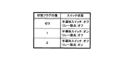
- FIG. 2 is a chart for explaining the status flag. As shown in FIG. 2, the value of the status flag being zero means that the semiconductor switches 20a and 20b and the relay contact 30 are off. The value of the status flag being 1 means that the semiconductor switches 20a and 20b are on and the relay contact 30 is off. The value of the status flag being 2 means that the semiconductor switches 20a and 20b are turned off and the relay contact 30 is turned on. The value of the state flag stored in the storage unit 57 is changed by the control unit 58.
- the storage unit 57 also stores a timer flag value used in the threshold value changing process.
- the value of the timer flag being zero means that the first timer 53 is not measuring time.
- the value of the timer flag being 1 means that the first timer 53 is measuring time.
- the value of the timer flag is changed by the control unit 58.
- connection processing blocking processing, switch change processing, and threshold value change processing will be described.
- the load current value Ia is less than the reference current value Ir, and the latch circuit 45 outputs a high level voltage.
- the voltage output from the latch circuit 45 is switched from the high level voltage to the low level voltage, and the semiconductor 5 is operated regardless of the operation of the microcomputer 5.
- the switches 20a and 20b and the relay contact 30 are switched off.
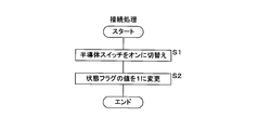
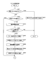
- FIG. 3 is a flowchart showing a connection processing procedure.
- the control unit 58 executes a connection process each time a connection signal is input to the input unit 55.
- the connection signal is input to the input unit 55 in a state where the semiconductor switches 20a and 20b and the relay contact 30 are off.
- the control unit 58 causes the drive circuit 40 to switch on the semiconductor switches 20a and 20b (step S1). Specifically, the control unit 58 instructs the output unit 50 to switch the voltage output from the output unit 50 to one input terminal of the AND circuit 41 to a high level voltage. Since the latch circuit 45 outputs a high level voltage, the AND circuit 41 outputs the voltage output from the output unit 50 as it is, and the drive circuit 40 switches on the semiconductor switches 20a and 20b.
- the control unit 58 ends step S1
- the semiconductor switches 20a and 20b are on and the relay contact 30 is off.
- the control unit 58 sets the value of the status flag to 1 (Step S2), and ends the connection process.
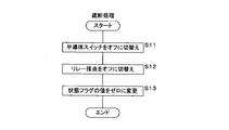
- FIG. 4 is a flowchart showing the procedure of the blocking process.
- the control unit 58 executes a blocking process each time a blocking signal is input to the input unit 55.
- the control unit 58 causes the drive circuit 40 to switch off the semiconductor switches 20a and 20b (step S11).
- the control unit 58 instructs the output unit 50 to switch the voltage output from the output unit 50 to one input terminal of the AND circuit 41 to a low level voltage. Since the latch circuit 45 outputs a high level voltage, the AND circuit 41 outputs the voltage output from the output unit 50 to the drive circuit 40 as it is, and the drive circuit 40 switches off the semiconductor switches 20a and 20b. .
- control unit 58 instructs the current supply unit 52 to switch off the relay contact 30 (step S12). Specifically, the current supply unit 52 opens the other end of the switch 46. Thereby, the current supply to the relay coil 31 is stopped, and the relay contact 30 is switched off. Thereafter, the control unit 58 changes the value of the state flag to zero (step S13) and ends the blocking process.
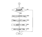
- FIG. 5 is a flowchart showing the procedure of threshold change processing.
- the control unit 58 periodically executes the threshold value changing process.
- the storage unit 57 stores threshold value information indicating the threshold value Ith.
- the control unit 58 sets the threshold value Ith indicated by the threshold value information to various current values.
- a first time T1, a second time T2, and a third time T3, which will be described later, are constant and stored in the storage unit 57 in advance.
- the second time T2 is longer than the first time T1
- the third time T3 is longer than the second time T2 (see FIG. 6).
- a first current value I1, a second current value I2, a third current value I3, and a fourth current value I4, which will be described later, are also constant and stored in the storage unit 57 in advance.
- the second current value I2 is smaller than the first current value I1
- the third current value I3 is smaller than the second current value I2
- the fourth current value I4 is smaller than the third current value I3 (see FIG. 6).
- the first current value I1 is smaller than the reference current value Ir.
- the reference current value Ir is a current value that is compared with the load current value Ia.
- the latch circuit 45 outputs a low level voltage when the load current value Ia is greater than or equal to the reference current value Ir.
- the control unit 58 first acquires current information from the A / D conversion unit 51 (step S21), and determines whether or not current is flowing through the switch circuit 2 (step S22). Specifically, the control unit 58 determines that a current is flowing through the switch circuit 2 when the switch current value Is indicated by the current information acquired in step S21 exceeds zero A. When the switch current value Is indicated by the current information acquired in step S ⁇ b> 21 is zero A, the control unit 58 determines that no current is flowing through the switch circuit 2.
- step S23 the control unit 58 instructs the first timer 53 to end timing.
- step S23 the control unit 58 does not execute step S23 and advances the process to step S24.
- control unit 58 After executing step S23, the control unit 58 sets the value of the timer flag to zero (step S24), and sets the threshold value Ith indicated by the threshold information to the reference current value Ir (step S25). Thereafter, the control unit 58 ends the threshold value changing process.
- step S26 determines whether or not the value of the timer flag is zero (step S26).
- the control unit 58 instructs the first timer 53 to start timing (step S27). ).
- the control unit 58 sets the value of the timer flag to 1 (step S28).
- the control unit 58 When the value of the timer flag is not zero, that is, when the value of the timer flag is 1 (S26: NO), or after executing step S28, the control unit 58 counts the time of the first timer 53. It is determined whether or not the first measured time is less than the first time T1 (step S29). When it is determined that the first measured time is less than the first time T1 (S29: YES), the control unit 58 sets the threshold Ith indicated by the threshold information to the first current value I1 (Step S30), and the threshold change process Exit.
- the control unit 58 determines whether or not the first time measurement is less than the second time T2 (> T1) (Ste S31). When it is determined that the first measured time is less than the second time T2 (S31: YES), the control unit 58 sets the threshold Ith indicated by the threshold information to the second current value I2 ( ⁇ I1) (step S32). Then, the threshold value changing process is terminated.
- the control unit 58 determines whether or not the first measured time is less than the third time T3 (> T2) (Ste S33). When it is determined that the first measured time is less than the third time T3 (S33: YES), the control unit 58 sets the threshold Ith indicated by the threshold information to the third current value I3 ( ⁇ I2) (step S34). Then, the threshold value changing process is terminated.
- the control unit 58 determines that the first timekeeping time is equal to or greater than the third time T3 (S33: NO)
- the control unit 58 sets the threshold value Ith indicated by the threshold value information to the fourth current value I4 ( ⁇ I3) (step S35). Then, the threshold value changing process is terminated.
- the first timer 53 continues to count time and the value of the timer flag is maintained at 1. The That is, the first timer 53 keeps counting until the switch current value Is flowing through the switch circuit 2 becomes zero A.
- FIG. 6 is a graph showing an example of the transition of the threshold value Ith.
- the transition of the threshold value Ith is indicated by a bold line, and the transition of the switch current value Is is indicated by a thin line.
- the vertical axis represents the current value, and the horizontal axis represents time.
- the threshold value Ith indicated by the threshold information is set to the reference current value Ir.
- the switch timer value Is exceeds zero A, so the first timer 53 starts measuring time. As described above, the first timer 53 continues timing until the switch current value Is becomes zero A. In the following description, it is assumed that the switch current value Is exceeds zero A as shown in FIG.
- the threshold Ith indicated by the threshold information is the first current value. Set to I1. While the elapsed time is not less than the first time T1 and less than the second time T2, the threshold Ith indicated by the threshold information is set to the second current value I2 ( ⁇ I1).
- the threshold Ith indicated by the threshold information is set to the third current value I3 ( ⁇ I2).
- the threshold Ith indicated by the threshold information is set to the fourth current value I4 ( ⁇ I3).
- the control unit 58 changes the threshold value Ith indicated by the threshold value information according to the length of time that has elapsed since the current flowed through the switch circuit 2.
- the control unit 58 functions as a changing unit.
- the resistance value of the load 12 is the smallest when the current supply to the load 12 is started, and increases as the time for supplying the current to the load 12 becomes longer. After the resistance value of the load 12 reaches a predetermined value, the resistance value of the load 12 is stabilized at the predetermined value as long as current supply to the load 12 is continued. Therefore, as shown in FIG. 6, immediately after the load 12 is operated, an inrush current flows through the switch circuit 2, and then the switch current value Is is stabilized.
- the threshold value Ith when the load 12 is activated is high.
- the threshold value Ith decreases as the elapsed time becomes longer. For this reason, inrush current generated immediately after the load 12 is activated is allowed to flow through the switch circuit 2. After the inrush current flows, the same current as the inrush current is prevented from flowing through the switch circuit 2.
- the control unit 58 causes the first timer 53 to stop timing and sets the threshold value Ith indicated by the threshold value information to the reference current value Ir.
- the control unit 58 periodically executes switch change processing. It is preferable that the cycle related to the switch change process coincides with the cycle related to the threshold change process, and it is preferable that the switch change process is executed immediately after the threshold change process is executed.
- the storage unit 57 stores period information indicating a maintenance period Pk in which the semiconductor switches 20a and 20b and the relay contact 30 are maintained in a state where the semiconductor switches 20a and 20b are off and the relay contact 30 is on. It is remembered.
- the maintenance period Pk indicated by the period information is set to various periods by the control unit 58.
- the control unit 58 first determines whether or not the value of the state flag is zero (step S41). When it is determined that the value of the state flag is zero (S41: YES), the control unit 58 instructs the second timer 54 to end timing (step S42). As a result, the second timer 54 finishes timing. After executing Step S42, the control unit 58 ends the switch change process. If the second timer 54 has not timed when the control unit 58 determines that the value of the state flag is zero, the control unit 58 ends the switch change process without executing step S42.
- the control unit 58 determines whether the value of the state flag is 2 (step S43). When it is determined that the value of the status flag is not 2, that is, the value of the status flag is 1 (S43: NO), the control unit 58 acquires current information from the A / D conversion unit 51 (step S44). Then, it is determined whether or not the switch current value Is indicated by the acquired current information is greater than or equal to the threshold value Ith indicated by the threshold information (step S45).
- the control unit 58 Since the threshold value Ith indicated by the threshold value information is changed by the threshold value changing process, it is set to one of the reference current value Ir, the first current value I1, the second current value I2, the third current value I3, and the fourth current value I4. Is set.
- the control unit 58 also functions as a determination unit. When determining that the switch current value Is is less than the threshold value Ith (S45: NO), the control unit 58 ends the switch change process.
- the control unit 58 does not determine that the switch current value Is is equal to or greater than the threshold value Ith in step S45.
- the switch current value Is becomes equal to or greater than the threshold value Ith, the voltage output from the latch circuit 45 is immediately switched from the high level voltage to the low level voltage, and the semiconductor switches 20a and 20b are independent of the operation of the microcomputer 5. And the relay contact 30 is switched off.
- the switch current value Is is zero A, which is less than the reference current value Ir.
- the control unit 58 instructs the current supply unit 52 to switch on the relay contact 30 (step S46). Specifically, the current supply unit 52 grounds the other end of the switch 46. The latch circuit 45 outputs a high level voltage, and the switch 46 is on. For this reason, when the current supply unit 52 grounds the other end of the switch 46, a current is supplied to the relay coil 31, and the relay contact 30 is switched on.
- the control unit 58 causes the drive circuit 40 to switch the semiconductor switches 20a and 20b to OFF as in step S11 of the shut-off process (step S47).
- the control unit 58 executes steps S46 and S47, the switch connecting the battery 11 and the load 12 is changed from the semiconductor switches 20a and 20b to the relay contact 30.
- the drive circuit 40 and the current supply unit 52 function as a switching unit.
- the control unit 58 sets the maintenance period Ps indicated by the period information (step S48).
- the storage unit 57 stores a period set as the sustain period Ps in association with the current value set as the threshold value Ith.
- the control unit 58 sets the sustain period Ps based on this correspondence and the threshold value Ith used in the determination in step S45.
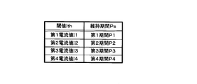
- FIG. 9 is a chart showing the correspondence between threshold values and maintenance periods.
- the storage unit 57 stores the first period P1, the second period P2, the third period P3, and the first current value I1, the second current value I2, the third current value I3, and the fourth current value I4 in association with each other.
- a fourth period P4 is stored.
- Each of the first period P1, the second period P2, the third period P3, and the fourth period P4 is constant.
- the second period P2 is shorter than the first period
- the third period P3 is shorter than the second period P2
- the fourth period P4 is shorter than the third period P3.
- step S48 the control unit 58 sets the maintenance period Ps indicated by the period information to a threshold value Ith indicated by the threshold information, that is, a period corresponding to the threshold value Ith used in the determination in step S45.
- a threshold value Ith indicated by the threshold information that is, a period corresponding to the threshold value Ith used in the determination in step S45.
- the control unit 58 sets the maintenance period Ps indicated by the period information to the first period P1.
- the control unit 58 also functions as a setting unit.
- Step S48 the control unit 58 instructs the second timer 54 to start timing (step S49).
- step S49 the controller 58 sets the value of the status flag to 2 (Step S50).
- the controller 58 determines that the value of the state flag is 2 (S43: YES), or after executing Step S50, the second time measured by the second timer 54 is the period information. It is determined whether or not it is longer than the maintenance period Ps shown (step S51).
- the control unit 58 ends the switch change process with the second timer 54 continuing the time measurement. As long as the value of the status flag is maintained at 2, the second timer 54 continues timing, and step S51 of the switch change process is repeatedly executed. Before the second timekeeping time becomes equal to or longer than the maintenance period Ps, when the state flag value becomes zero, the switch change processing step S42 is executed, and the second timer 54 ends the timekeeping. .
- the control part 58 will instruct
- the control unit 58 causes the drive circuit 40 to switch on the semiconductor switches 20a and 20b (step S53), and causes the current supply unit 52 to switch to step S12 of the cutoff process.
- the relay contact 30 is switched off (step S54).
- the control unit 58 executes steps S53 and S54, the switch connecting the battery 11 and the load 12 returns from the relay contact 30 to the semiconductor switches 20a and 20b. Thereafter, the control unit 58 sets the value of the status flag to 1 (step S55), and ends the switch change process.
- control unit 58 causes the drive circuit 40 and the current supply unit 52 to switch the semiconductor switches 20a and 20b and the relay contact 30 on or off, The power supply via the switch circuit 2 and the relay contact 30 is controlled.
- FIG. 10 is a graph showing an example of transition of the switch current value Is.
- the transition of the threshold value Ith is indicated by a bold line, and the transition of the switch current value Is is indicated by a thin line.
- the vertical axis represents the current value, and the horizontal axis represents time.
- the threshold value Ith is changed according to the elapsed time after the current flows through the semiconductor switches 20a and 20b in the threshold value changing process.
- the switch current value Is rises due to various causes, for example, temporary contact between the conductor connecting the drain of the semiconductor switch 20b and one end of the load 12, and the switch current value Is exceeds a threshold value.
- the control unit 58 determines that the switch current value Is is equal to or greater than the threshold value Ith, the relay contact 30 is switched on, and the semiconductor switches 20a and 20b are switched off. Thereby, since the switch current value Is becomes zero A, in the threshold value changing process, the threshold value Ith indicated by the threshold value information is returned to the reference current value Ir.
- the control unit 58 sets the sustain period Ps when it is determined that the switch current value Is is equal to or greater than the threshold value Ith.
- the threshold value Ith when the switch current value Is is determined to be equal to or greater than the threshold value Ith is set to the third current value I3. For this reason, the sustain period Ps indicated by the period information is set to the third period P3 (see FIG. 9).
- the second timer 54 starts measuring time. Unless the cutoff signal is input to the input unit 55 and the cutoff process is performed, the semiconductor switches 20a and 20b until the sustain period Ps elapses after the control unit 58 determines that the switch current value Is is equal to or greater than the threshold value Ith. Is kept off and the relay contact 30 is kept on. When the shut-off process is executed before the maintenance period Ps elapses, the semiconductor switches 20a and 20b and the relay contact 30 are switched off by the shut-off process, and the second timer 54 finishes timing by the switch change process.
- the semiconductor switches 20a and 20b are switched on and the relay contact 30 is switched off. Thereby, the current flows again through the switch circuit 2, and in the threshold value changing process, the threshold value Ith is changed again according to the elapsed time after the current flows through the switch circuit 2.
- the temperature of the switch circuit 2 is as long as the amount of heat generated by the on-resistance of the semiconductor switches 20a and 20b exceeds the amount of heat released from the semiconductor switches 20a and 20b. To rise.
- the temperature of the switch circuit 2 is higher as the switch current value Is is higher, and the temperature is higher as the period of current flowing through the switch circuit 2 is longer.
- the threshold value Ith is changed according to the length of time that has elapsed since the current flowed through the switch circuit 2. Specifically, the threshold value Ith decreases as the elapsed time increases. Therefore, the relay contact 30 can be switched on and the semiconductor switches 20a and 20b can be switched off at an appropriate timing, for example, when the temperature of the switch circuit 2 substantially matches the predetermined temperature. .
- the maintenance period Ps is set according to the threshold value Ith used in the determination in step S45 of the connection change process. Specifically, the sustain period Ps is longer as the threshold value Ith used in step S45 is larger. Therefore, the semiconductor switches 20a and 20b can be turned back on and the relay contact 30 can be turned off in a state where the temperature of the switch circuit 2 is sufficiently lower than the predetermined temperature described above.
- the semiconductor switches 20a and 20b are FETs, parasitic diodes are formed between the drains and sources of the semiconductor switches 20a and 20b.
- the cathode and anode of the parasitic diode are connected to the drain and source, respectively.
- the cathode and anode of the parasitic diode are connected to the source and drain, respectively.
- the semiconductor switches 20a and 20b are both N-channel FETs, and the drain of the semiconductor switch 20a is connected to the drain of the semiconductor switch 20b. Therefore, as long as the semiconductor switches 20a and 20b are off, even if the connection of the battery 11 is wrong, current is passed through the parasitic diode formed between the drain and source of each of the semiconductor switches 20a and 20b. There is no flow.
- the switch circuit 2 is not limited to the configuration in which the drain of the semiconductor switch 20a is connected to the drain of the semiconductor switch 20b.
- the semiconductor switches 20a and 20b may be the same type of FET, they may be P-channel type FETs. Even when configured as described above, as long as the semiconductor switches 20a and 20b are off, no current flows through the parasitic diodes formed in the semiconductor switches 20a and 20b.
- the drive circuit 40 switches on the semiconductor switches 20a and 20b by lowering the voltage value of the gates of the semiconductor switches 20a and 20b.
- the semiconductor switches 20a and 20b are switched off by increasing the voltage value of the gate.
- the number of semiconductor switches included in the switch circuit 2 is not limited to two, and may be one.
- the semiconductor switches are not limited to FETs, and may be bipolar transistors, for example. Even in such a configuration, the relay contact 30 can be switched on and the semiconductor switches 20a and 20b can be switched off at an appropriate timing. In a sufficiently low state, the semiconductor switches 20a and 20b can be turned back on and the relay contact 30 can be turned off.
- the number of periods set as the maintenance period Ps is not limited to four, and may be two, three, five or more.
- the setting of the sustain period Ps is not limited to the setting using the table shown in FIG.
- the sustain period Ps may be set using an arithmetic expression having the threshold value Ith as a variable. In this case, in step S48 of the switch change process, the period is calculated by substituting the threshold value Ith indicated by the threshold information into the arithmetic expression, and the maintenance period Ps indicated by the period information is set to the calculated period. Further, the maintenance period Ps may be fixed.
- the number of current values set as the threshold value Ith is not limited to 4 except for the reference current value Ir, and may be 2, 3 or 5 or more. In this case, the number of times such as the first time T1 or the second time T2 compared with the first time measurement time is a number obtained by subtracting 1 from the number of current values.
- the threshold value Ith may be set using an arithmetic expression having a variable as the first time measurement time, that is, the elapsed time after the current flows through the switch circuit 2. In this case, in the threshold value changing process, the control unit 58 determines that the value of the timer flag is not zero (S26: NO), or after executing step S28, sets the first time measurement time to the above-described arithmetic expression. The current value is calculated by substitution, and the threshold value Ith indicated by the threshold information is set to the calculated current value.
- the configuration for detecting the switch current value Is is not limited to the configuration using the current sensor 47.
- the switch current value Is is calculated from the voltage value between both ends of a resistor connected in series to the switch circuit 2. It may be a configuration.
- the relay contact 30 is connected in parallel to the series circuit of the switch circuit 2 and the resistor, and the relay contact 30 is connected to the switch circuit 2 substantially in parallel.
- the load 12 is not limited to a load whose resistance value gradually increases after the current supply is started.
Landscapes
- Engineering & Computer Science (AREA)
- Power Engineering (AREA)
- Electronic Switches (AREA)
Priority Applications (3)
| Application Number | Priority Date | Filing Date | Title |
|---|---|---|---|
| CN201780028092.6A CN109074989B (zh) | 2016-05-26 | 2017-05-16 | 供电控制装置、供电控制方法及计算机程序 |
| DE112017002636.9T DE112017002636T5 (de) | 2016-05-26 | 2017-05-16 | Stromversorgungssteuervorrichtung, Stromversorgungssteuerverfahren und Computerprogramm |
| US16/303,972 US11004626B2 (en) | 2016-05-26 | 2017-05-16 | Power supply control device, power supply control method, and computer program |
Applications Claiming Priority (2)
| Application Number | Priority Date | Filing Date | Title |
|---|---|---|---|
| JP2016105476A JP6620674B2 (ja) | 2016-05-26 | 2016-05-26 | 給電制御装置、給電制御方法及びコンピュータプログラム |
| JP2016-105476 | 2016-05-26 |
Publications (1)
| Publication Number | Publication Date |
|---|---|
| WO2017204038A1 true WO2017204038A1 (ja) | 2017-11-30 |
Family
ID=60412374
Family Applications (1)
| Application Number | Title | Priority Date | Filing Date |
|---|---|---|---|
| PCT/JP2017/018363 Ceased WO2017204038A1 (ja) | 2016-05-26 | 2017-05-16 | 給電制御装置、給電制御方法及びコンピュータプログラム |
Country Status (5)
| Country | Link |
|---|---|
| US (1) | US11004626B2 (enExample) |
| JP (1) | JP6620674B2 (enExample) |
| CN (1) | CN109074989B (enExample) |
| DE (1) | DE112017002636T5 (enExample) |
| WO (1) | WO2017204038A1 (enExample) |
Cited By (1)
| Publication number | Priority date | Publication date | Assignee | Title |
|---|---|---|---|---|
| WO2020183700A1 (ja) * | 2019-03-14 | 2020-09-17 | オムロン株式会社 | 制御装置、及び太陽光発電システム |
Families Citing this family (6)
| Publication number | Priority date | Publication date | Assignee | Title |
|---|---|---|---|---|
| JP7149699B2 (ja) | 2017-11-01 | 2022-10-07 | 日東電工株式会社 | 熱伝導性粘着シート |
| JP6788060B2 (ja) * | 2019-03-29 | 2020-11-18 | 住友電装株式会社 | 給電制御装置、開放検知方法及びコンピュータプログラム |
| CN114128070B (zh) * | 2019-07-17 | 2024-10-11 | 松下知识产权经营株式会社 | 电力切断装置 |
| JP7196826B2 (ja) * | 2019-12-13 | 2022-12-27 | 株式会社オートネットワーク技術研究所 | スイッチ装置、電流判定方法及びコンピュータプログラム |
| DE102023109447A1 (de) * | 2023-04-14 | 2024-10-17 | Infineon Technologies Ag | Treiberschaltung zum ansteuern eines halbleiterschalters |
| US20250274116A1 (en) * | 2024-02-28 | 2025-08-28 | Advanced Energy Industries, Inc. | Over-current protection for a power supply |
Citations (4)
| Publication number | Priority date | Publication date | Assignee | Title |
|---|---|---|---|---|
| JPS6149335A (ja) * | 1984-08-16 | 1986-03-11 | オムロン株式会社 | 多極負荷開閉装置 |
| JPH11213830A (ja) * | 1998-01-22 | 1999-08-06 | Matsushita Electric Works Ltd | 電子式スイッチ |
| JP2003338239A (ja) * | 2002-04-12 | 2003-11-28 | Lg Industrial Syst Co Ltd | ハイブリッド直流電磁接触器 |
| WO2011052606A1 (ja) * | 2009-10-27 | 2011-05-05 | パナソニック電工株式会社 | ハイブリッドリレー |
Family Cites Families (11)
| Publication number | Priority date | Publication date | Assignee | Title |
|---|---|---|---|---|
| JPS5935748B2 (ja) | 1979-11-08 | 1984-08-30 | 不二空機株式会社 | 衝撃作動空気工具 |
| JP3384522B2 (ja) * | 1996-07-30 | 2003-03-10 | 矢崎総業株式会社 | スイッチング装置 |
| KR101877377B1 (ko) | 2010-04-23 | 2018-07-11 | 가부시키가이샤 한도오따이 에네루기 켄큐쇼 | 반도체 장치의 제작 방법 |
| JP5811055B2 (ja) * | 2012-07-11 | 2015-11-11 | 株式会社デンソー | バッテリシステム制御装置 |
| JP5983171B2 (ja) * | 2012-08-10 | 2016-08-31 | 株式会社Gsユアサ | スイッチ故障診断装置、蓄電装置 |
| JP6472076B2 (ja) * | 2015-03-06 | 2019-02-20 | Fdk株式会社 | 負荷電流制御装置 |
| WO2016181495A1 (ja) * | 2015-05-12 | 2016-11-17 | 日産自動車株式会社 | 電源システム |
| MY170641A (en) * | 2016-01-12 | 2019-08-21 | Nissan Motor | Power supply system and method for controlling same |
| US11538943B2 (en) * | 2016-09-12 | 2022-12-27 | Phoenix Contact Gmbh & Co. Kg | Photovoltaic system, direct current hybrid switching device, use and method for switching a photovoltaic string on and off |
| JP6665757B2 (ja) * | 2016-11-08 | 2020-03-13 | 株式会社デンソー | 電源制御装置、及び電池ユニット |
| JP6669097B2 (ja) * | 2017-02-14 | 2020-03-18 | 株式会社オートネットワーク技術研究所 | 給電制御装置 |
-
2016
- 2016-05-26 JP JP2016105476A patent/JP6620674B2/ja not_active Expired - Fee Related
-
2017
- 2017-05-16 WO PCT/JP2017/018363 patent/WO2017204038A1/ja not_active Ceased
- 2017-05-16 US US16/303,972 patent/US11004626B2/en not_active Expired - Fee Related
- 2017-05-16 CN CN201780028092.6A patent/CN109074989B/zh not_active Expired - Fee Related
- 2017-05-16 DE DE112017002636.9T patent/DE112017002636T5/de not_active Withdrawn
Patent Citations (5)
| Publication number | Priority date | Publication date | Assignee | Title |
|---|---|---|---|---|
| JPS6149335A (ja) * | 1984-08-16 | 1986-03-11 | オムロン株式会社 | 多極負荷開閉装置 |
| JPH11213830A (ja) * | 1998-01-22 | 1999-08-06 | Matsushita Electric Works Ltd | 電子式スイッチ |
| JP2003338239A (ja) * | 2002-04-12 | 2003-11-28 | Lg Industrial Syst Co Ltd | ハイブリッド直流電磁接触器 |
| WO2011052606A1 (ja) * | 2009-10-27 | 2011-05-05 | パナソニック電工株式会社 | ハイブリッドリレー |
| JP5669086B2 (ja) * | 2009-10-27 | 2015-02-12 | パナソニックIpマネジメント株式会社 | ハイブリッドリレー |
Cited By (4)
| Publication number | Priority date | Publication date | Assignee | Title |
|---|---|---|---|---|
| WO2020183700A1 (ja) * | 2019-03-14 | 2020-09-17 | オムロン株式会社 | 制御装置、及び太陽光発電システム |
| JPWO2020183700A1 (ja) * | 2019-03-14 | 2021-12-16 | オムロン株式会社 | 制御装置、及び太陽光発電システム |
| JP7367752B2 (ja) | 2019-03-14 | 2023-10-24 | オムロン株式会社 | 制御装置、及び太陽光発電システム |
| US11886217B2 (en) | 2019-03-14 | 2024-01-30 | Omron Corporation | Control device and solar power generation system |
Also Published As
| Publication number | Publication date |
|---|---|
| DE112017002636T5 (de) | 2019-04-11 |
| US11004626B2 (en) | 2021-05-11 |
| CN109074989A (zh) | 2018-12-21 |
| JP2017212146A (ja) | 2017-11-30 |
| JP6620674B2 (ja) | 2019-12-18 |
| US20200402738A1 (en) | 2020-12-24 |
| CN109074989B (zh) | 2019-08-30 |
Similar Documents
| Publication | Publication Date | Title |
|---|---|---|
| JP6620674B2 (ja) | 給電制御装置、給電制御方法及びコンピュータプログラム | |
| KR101311690B1 (ko) | 단락 검출 회로 및 단락 검출 방법 | |
| JP6381023B2 (ja) | 突入電流制限回路 | |
| CN105098872B (zh) | 充放电控制电路和电池装置 | |
| US20180304827A1 (en) | Current control device, current control method, and computer program | |
| JP2017118791A (ja) | 給電制御装置 | |
| KR20140111611A (ko) | 충방전 제어 회로, 충방전 제어장치 및 배터리 장치 | |
| JP6904229B2 (ja) | 給電制御装置及び給電制御方法 | |
| JP7067033B2 (ja) | 給電制御装置、給電制御方法及びコンピュータプログラム | |
| US10910183B2 (en) | Power supply control device, power supply control method, and computer program | |
| CN114731041B (zh) | 开关装置、电流判定方法和计算机程序 | |
| JP2015220771A (ja) | 充放電制御回路およびバッテリ装置 | |
| WO2018168392A1 (ja) | 給電制御装置、給電制御方法及びコンピュータプログラム | |
| CN114788114B (zh) | 供电控制装置 | |
| JP2014155261A (ja) | 半導体駆動装置 | |
| JP5780270B2 (ja) | スイッチング素子の駆動回路 | |
| WO2021192898A1 (ja) | 電流制御装置、スイッチ制御装置、電流制御方法及びコンピュータプログラム |
Legal Events
| Date | Code | Title | Description |
|---|---|---|---|
| 121 | Ep: the epo has been informed by wipo that ep was designated in this application |
Ref document number: 17802630 Country of ref document: EP Kind code of ref document: A1 |
|
| 122 | Ep: pct application non-entry in european phase |
Ref document number: 17802630 Country of ref document: EP Kind code of ref document: A1 |