WO2017203857A1 - Processing apparatus, image sensor, and system - Google Patents
Processing apparatus, image sensor, and system Download PDFInfo
- Publication number
- WO2017203857A1 WO2017203857A1 PCT/JP2017/014726 JP2017014726W WO2017203857A1 WO 2017203857 A1 WO2017203857 A1 WO 2017203857A1 JP 2017014726 W JP2017014726 W JP 2017014726W WO 2017203857 A1 WO2017203857 A1 WO 2017203857A1
- Authority
- WO
- WIPO (PCT)
- Prior art keywords
- image
- output
- sensor
- sensors
- data
- Prior art date
Links
Images


Classifications
-
- H—ELECTRICITY
- H04—ELECTRIC COMMUNICATION TECHNIQUE
- H04N—PICTORIAL COMMUNICATION, e.g. TELEVISION
- H04N5/00—Details of television systems
- H04N5/04—Synchronising
-
- H—ELECTRICITY
- H04—ELECTRIC COMMUNICATION TECHNIQUE
- H04N—PICTORIAL COMMUNICATION, e.g. TELEVISION
- H04N23/00—Cameras or camera modules comprising electronic image sensors; Control thereof
- H04N23/60—Control of cameras or camera modules
-
- H—ELECTRICITY
- H04—ELECTRIC COMMUNICATION TECHNIQUE
- H04N—PICTORIAL COMMUNICATION, e.g. TELEVISION
- H04N23/00—Cameras or camera modules comprising electronic image sensors; Control thereof
- H04N23/90—Arrangement of cameras or camera modules, e.g. multiple cameras in TV studios or sports stadiums
-
- H—ELECTRICITY
- H04—ELECTRIC COMMUNICATION TECHNIQUE
- H04N—PICTORIAL COMMUNICATION, e.g. TELEVISION
- H04N5/00—Details of television systems
- H04N5/04—Synchronising
- H04N5/06—Generation of synchronising signals
- H04N5/067—Arrangements or circuits at the transmitter end
- H04N5/073—Arrangements or circuits at the transmitter end for mutually locking plural sources of synchronising signals, e.g. studios or relay stations
- H04N5/0733—Arrangements or circuits at the transmitter end for mutually locking plural sources of synchronising signals, e.g. studios or relay stations for distributing synchronisation pulses to different TV cameras
-
- H—ELECTRICITY
- H04—ELECTRIC COMMUNICATION TECHNIQUE
- H04N—PICTORIAL COMMUNICATION, e.g. TELEVISION
- H04N7/00—Television systems
- H04N7/18—Closed-circuit television [CCTV] systems, i.e. systems in which the video signal is not broadcast
-
- H—ELECTRICITY
- H04—ELECTRIC COMMUNICATION TECHNIQUE
- H04N—PICTORIAL COMMUNICATION, e.g. TELEVISION
- H04N7/00—Television systems
- H04N7/18—Closed-circuit television [CCTV] systems, i.e. systems in which the video signal is not broadcast
- H04N7/181—Closed-circuit television [CCTV] systems, i.e. systems in which the video signal is not broadcast for receiving images from a plurality of remote sources
Definitions
- the present disclosure relates to processing apparatuses, image sensors, and systems.
- connection between devices such as, for example, connection between a processor and a sensor
- technologies for connection between devices is, for example, a technique disclosed in PTL1 described below.
- CSI-2 Camera Serial Interface 2
- MIPI Mobile Industry Processor Interface
- a novel and improved processing apparatus in which, in a case where a processing apparatus is connected to a plurality of image sensors by a data bus, respective images which are captured by the plurality of image sensors during a predetermined period of time can be transmitted through the data bus.
- a processing apparatus including a processing unit that is connectable to a data bus, and performs output control on respective images captured by a plurality of image sensors connected to the data bus during a predetermined period of time. A timing of output of the image performed by each of the plurality of image sensors is changed by the output control.
- an image sensor that is connectable to a data bus to which another image sensor is connected, and outputs an image captured during a predetermined period of time, at an output timing based on control information.
- a system including: a plurality of image sensors that are connected to a data bus, and a processing apparatus that is connected to the data bus.
- the processing apparatus includes a processing unit that performs output control on respective images captured by the plurality of image sensors during a predetermined period of time, and a timing of output of the image in each of the plurality of image sensors is changed by the output control.
- a processing apparatus in a case where a processing apparatus is connected to a plurality of image sensors by a data bus, respective images which are captured by the plurality of image sensors during a predetermined period of time can be transmitted through the data bus.
- FIG. 1 is an explanatory diagram showing an example of a configuration of a system according to the present embodiment.
- FIG. 2 is an explanatory diagram showing an example of a case where images are transmitted by time-division multiplexing on a data bus to which a plurality of sensors are connected.
- FIG. 3 is an explanatory diagram for describing an overview of transmission of images in a system according to the present embodiment.
- FIG. 4 is an explanatory diagram showing an example of a configuration of a sensor included in a system according to the present embodiment.
- FIG. 5 shows an example of image data captured by a sensor included in a system according to the present embodiment.
- FIG. 6 shows an example of a packet sequence of image data transmitted on a data bus included in a system according to the present embodiment.
- FIG. 1 is an explanatory diagram showing an example of a configuration of a system according to the present embodiment.
- FIG. 2 is an explanatory diagram showing an example of a case where images are transmitted by time-division multiplex
- FIG. 7 shows an example of a frame buffer allocated in a memory included in a system according to the present embodiment.
- FIG. 8 is an explanatory diagram showing an example of an operation of a sensor 200 equipped with an imaging device which supports the rolling shutter method.
- FIG. 9 is an explanatory diagram showing an example of an operation of a sensor equipped with an imaging device supporting the rolling shutter method.
- FIG. 10 is an explanatory diagram showing an example of operations of two sensors each equipped with an imaging device supporting the rolling shutter method.
- FIG. 11 is an explanatory diagram showing an example of an operation of a sensor equipped with an imaging device supporting the global shutter method.
- FIG. 12 is an explanatory diagram showing an example of an operation of a sensor equipped with an imaging device supporting the global shutter method.
- FIG. 13 is an explanatory diagram showing a first example of output of an image performed by a sensor in a system according to the present embodiment.
- FIG. 14 is an explanatory diagram showing a second example of output of an image performed by a sensor in a system according to the present embodiment.
- FIG. 15 is a flowchart showing an example of a process involved in control of output of an image performed by a processor included in a system according to the present embodiment (a process involved in a control method according to according to the present embodiment).
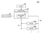
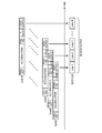
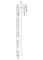
- FIG. 1 is an explanatory diagram showing an example of a configuration of a system 1000 according to the present embodiment.
- the system 1000 include communication apparatuses (e.g., a smartphone, etc.), mobile apparatuses (e.g., a drone (an apparatus which can be remotely operated or autonomously operate), automobile, etc.), and the like.
- communication apparatuses e.g., a smartphone, etc.
- mobile apparatuses e.g., a drone (an apparatus which can be remotely operated or autonomously operate), automobile, etc.
- application examples of the system 1000 are not limited to those described above. Other application examples of the system 1000 will be described below.
- the system 1000 has, for example, a processor 100 (a processing apparatus according to the present embodiment), a plurality of sensors 200A, 200B, . . . (an image sensor according to the present embodiment) which have a function of outputting an image, a memory 300, and a display device 400.
- the plurality of sensors 200A, 200B, . . . may be collectively referred to as “sensors 200,” or one of the plurality of sensors 200A, 200B, . . . may be representatively referred to as a “sensor 200.”
- the system 1000 shown in FIG. 1 has two or more sensors 200
- the number of sensors 200 included in the system according to the present embodiment is not limited to the example shown in FIG. 1.
- the system according to the present embodiment may have any number of sensors 200 that are at least two sensors 200, such as two sensors 200, three sensors 200, or the like.
- a case where an image is output by two of the plurality of sensors 200 included in the system 1000 will be mainly described by way of example.
- the processor 100 and of the respective sensors 200 are electrically connected together by a single data bus B1.
- the data bus B1 is a single signal transmission path which connects the processor 100 and the respective sensors 200 together.
- image data data indicating an image output by each sensor 200 (may hereinafter be referred to as “image data”) is transmitted from the sensor 200 to the processor 100 through the data bus B1.
- a signal is transmitted through the data bus B1 in accordance with any standard that allows for time-division multiplexing transmission of data, such as the CSI-2 standard, PCI Express, or the like.
- any standard that allows for time-division multiplexing transmission of data such as the CSI-2 standard, PCI Express, or the like.
- the processor 100 and the respective sensors 200 are also connected together by a control bus B2 different from the data bus B1.
- the control bus B2 is another signal transmission path which connects the processor 100 and the respective sensors 200 together.
- control information (described below) which is output by the processor 100 is transmitted from the processor 100 to the sensors 200 through the control bus B2.
- FIG. 1 shows the example in which the processor 100 and the respective sensors 200 are connected together by the single control bus B2, the system according to the present embodiment can have a configuration in which a separate control bus is provided for each sensor 200.
- the present disclosure is not limited to the configuration in which the processor 100 transmits and receives control information (described below) to and from the respective sensors 200 through the control bus B2.
- control information described below
- a configuration may be employed in which control information (described below) is transmitted and received through wireless communication having any communication scheme that can be used to transmit and receive control information (described below).
- FIG. 2 is an explanatory diagram showing an example of a case where images are transmitted by time-division multiplexing on a data bus to which a plurality of sensors are connected.
- FIG. 2 shows an example of time-division multiplexing transmission in a case where two sensors each having an imaging device (a sensor #1 and a sensor #2 shown in FIG. 2) output an image to the data bus immediately after performing image capture.
- the sensors have different image capture timings, and therefore, the two sensors do not capture images at the same time (or captured images are not considered to be captured at the same time).
- time-division multiplexing transmission is achieved by causing a plurality of sensors to perform image capture during a predetermined period of time, and output images at different timings.
- control of image capture performed by a plurality of sensors, and control of timings at which the plurality of sensors output images, are performed by, for example, the processor 100.
- examples of the meaning of the wording “during a predetermined period of time” according to the present embodiment include “during a 1-frame period,” “during a period of time corresponding to a difference of several lines of an image,” “at the same time,” and the like.
- the meaning of the wording “during a predetermined period of time” according to the present embodiment is not limited to the above examples.
- the meaning of the wording “during a predetermined period of time” according to the present embodiment may, for example, be “during an arbitrary period of time” which is set by a designer, user, or the like of the system 1000, regarding image capture performed by a plurality of sensors during that period of time as being performed at the same time.
- Image capture performed by a plurality of sensors during a predetermined period of time is, for example, controlled according to control information for controlling image capture which is transmitted by the processor 100 through the control bus B2.
- the control information for controlling image capture is, for example, data containing an image capture command (an example of a process command).
- control information for controlling image capture may contain a synchronization signal for causing a plurality of sensors to operate synchronously.
- image capture performed by sensors is controlled according to the control information containing a synchronization signal, it can be said that “images captured by a plurality of sensors during a predetermined period of time are images which are synchronously captured by the plurality of image sensors.”
- the synchronization signal may be transmitted by one of the plurality of sensors 200 included in the system 1000 that functions as a master.
- FIG. 3 is an explanatory diagram for describing an overview of transmission of images in the system 1000 according to the present embodiment.
- FIG. 3 shows an example in which two sensors (a sensor #1 and a sensor #2 shown in FIG. 3) each have an imaging device, and capture images synchronously on the basis of reception of a synchronization signal Vsync.
- the synchronization signal Vsync is transmitted from the processor 100 through the control bus B2, for example. Since the synchronization signal Vsync is transmitted from the processor 100 through the control bus B2, a plurality of sensors 200 can be synchronously operated in the system 1000. In other words, in the system 1000, for example, image capture and image output performed by a plurality of sensors 200 can be synchronized under the control of the processor 100 through the control bus B2.
- the method of synchronously operating a plurality of sensors 200 in the system 1000 is not limited to the above “method in which the processor 100 transmits a synchronization signal Vsync to all sensors 200 included in the system 1000.”
- one of the plurality of sensors 200 may function as a master so that the plurality of sensors 200 are synchronized.
- the sensor 200 functioning as a master transmits a synchronization signal Vsync to the other sensors 200 (sensors 200 functioning as a slave).
- the synchronous operation of the plurality of sensors 200 is achieved by the other sensors 200 receiving a synchronization signal Vsync transmitted by the sensor 200 functioning as a master.
- the transmission and reception of a synchronization signal Vsync between each sensor 200 are performed through, for example, a 1-bit dedicated line between each sensor 200.
- the two sensors perform image capture synchronously according to the synchronization signal Vsync. Thereafter, the two sensors output captured images at different timings so that pieces of data indicating the captured images do not collide with each other on the data bus B1.
- the sensor #1 outputs an image to the data bus immediately after performing image capture
- the sensor #2 outputs an image to the data bus after a delay of a delay amount indicated by “wait” in FIG. 3 from performing image capture.
- images having the same image capture timing between sensors can be transmitted by time-division multiplexing on the data bus B1.
- the processor 100 includes one or more processors, various processing circuits, or the like which include a computation circuit, such as a microprocessing unit (MPU) or the like.
- the processor 100 also has, for example, terminals to which external buses are connected, such as a terminal to which the data bus B1 can be connected, a terminal to which the control bus B2 can be connected, and the like, and can be connected to external buses, such as the data bus B1 and the like.
- the processor 100 is driven with power supplied from an internal power supply (not shown), such as a battery or the like, included in the system 1000, or power supplied from a power supply external to the system 1000.
- the processor 100 is an example of the processing apparatus according to the present embodiment.
- the processing apparatus according to the present embodiment is applicable to any circuits and devices that can perform a process (process involved in a control method according to the present embodiment) performed by a processing unit described below.
- the processor 100 performs “control of output of images captured by a plurality of sensors 200 connected to the data bus B1 during a predetermined period of time (the control method according to according to the present embodiment control).”
- the output control of an image is performed by, for example, a processing unit 102 included in the processor 100.
- a specific processor or a specific processing circuit
- a plurality of processors or a plurality of processing circuits which perform the output control of an image, function as the processing unit 102.
- the processing unit 102 is in charge of a portion of the functionality of the processor 100 for the sake of convenience. Therefore, in the processor 100, for example, the output control of an image according to the present embodiment may be performed by a plurality of functional blocks. In the description that follows, an example will be described in which the output control of an image according to the present embodiment is performed by the processing unit 102.
- Example of output control of image according to the present embodiment
- the processing unit 102 performs the output control of an image by transmitting control information to each sensor 200.
- the control information according to the present embodiment includes, for example, identification information indicating a sensor 200, and information for controlling the sensor 200.
- the identification information according to the present embodiment is, for example, any data that can be used to identify a sensor 200, such as an ID set for the sensor 200 or the like. A specific example of information for control according to the present embodiment will be described below.
- the control information is transmitted through, for example, the control bus B2 as described above.
- control information transmitted by the processing unit 102 is, for example, recorded into a register (an example of a recording medium) included in each sensor 200. Thereafter, as described below, the sensors 200 output images which have been captured during a predetermined period of time, at output timings based on the control information stored in their registers.
- the processing unit 102 performs any of control according to a first example described below in (1) to control according to a third example described below in (3), for example. Note that examples of output of images in the system 1000 which is achieved by image output control according to the present embodiment will be described below.
- control of delay The processing unit 102 controls a delay in output of an image performed by a sensor 200.
- the processing unit 102 controls a delay in output of an image performed by a sensor 200, by transmitting, to the sensor 200, the control information containing data indicating the amount of a delay in output of an image (first output information, an example of information for control).
- the data indicating the amount of a delay in output of an image may hereinafter be referred to as “data indicating a delay amount”
- data directly indicating a delay amount using a numerical value or the like e.g., data indicating a delay time, etc.
- data indirectly indicating a delay amount e.g., an ID associated with the delay amount, etc.
- Second example of image output control control of transmission interval
- the processing unit 102 controls intervals at which packets are output when the sensor 200 outputs an image.
- Packets used in output of an image are, for example, data in units of a line in the image.
- the processing unit 102 controls intervals at which packets are output when the sensor 200 outputs an image, by transmitting, to the sensor 200, the control information containing data (second output information, an example of information for control) indicating intervals (data pitch) at which packets are output when an image is output.
- the data indicating intervals at which packets are output when the sensor 200 outputs an image may hereinafter be referred to as “data indicating an output interval between packets”) include data directly indicating the output interval using a numerical value (e.g., data indicating a time interval, etc.), data indirectly indicating the output interval (e.g., an ID associated with the output interval, etc.), and the like.
- the processing unit 102 may perform both the control according to the first example described above in (1) and the control according to the second example described above in (2).
- the processing unit 102 performs the control according to the first example described above in (1) to the control according to the third example described above in (3), for example.
- the processor 100 is, for example, equipped with the processing unit 102 in order to perform a process involved in the above image output control (a process involved in the control method according to according to the present embodiment).
- processor 100 performing the control according to the first example described above in (1) to the control according to the third example described above in (3), one or both of a delay in output of an image and an output interval between packets used in output of an image are controlled according to the control information stored in the register or the like in each sensor 200.
- the processor 100 can change an image output timing in each sensor 200 (image sensor) by performing the process involved in the image output control.
- an image output timing in each sensor 200 can be changed by the processor 100 performing the image output control.
- the process performed by the processor 100 is not limited to the above process involved in the image output control.
- the processor 100 can control an image to be output by transmitting the control information to each sensor 200.
- the control of an image to be output is performed by, for example, the processing unit 102.
- the control of an image to be output according to the present embodiment is, for example, one or both of control of a size of an image to be output by each sensor 200 and control of a frame rate of an image to be output by each sensor 200.
- the processor 100 transmits control information containing one or both of data indicating an image size and data indicating a frame rate (an example of information for control) to a sensor 200, to control an image to be output by the sensor 200.
- control information containing one or both of data indicating an image size and data indicating a frame rate (an example of information for control) to a sensor 200, to control an image to be output by the sensor 200.
- the processor 100 can perform various processes such as a process involved in control of recording of image data received via the data bus B1 into a recording medium such as the memory 300 or the like, a process involved in control of displaying of an image on a display screen of the display device 400, a process of executing any application software, and the like.
- the process involved in control of recording is, for example, a “process of transferring control data containing a record instruction and data to be recorded into a recording medium, to a recording medium such as the memory 300 or the like.”
- the process involved in control of displaying is, for example, a “process of transferring control data containing a display instruction and data to be displayed on a display screen, to a display device such as the display device 400 or the like.”
- the sensors 200 are an image sensor.
- the image sensor according to the present embodiment includes, for example, an imaging device, such as a digital still camera, digital video camera, stereo camera, or the like, or any sensor device having an image capturing function, such as an infrared sensor, range imaging sensor, or the like, to have a function of outputting an image generated by the image capturing.
- an image generated by the sensor 200 corresponds to data indicating the result of sensing performed by the sensor 200.
- a sensor 200 is connected to the data bus B1 to which other sensors 200 are connected.
- image capture performed by the sensors 200 is, for example, performed according to the control information received through the control bus B2, under the control of the processor 100.
- image capture performed by one sensor 200 and image capture performed by another sensor 200 included in the system 1000 are performed during a predetermined period of time.
- the sensors 200 output images at output timings based on the control information.
- image capture performed by one sensor 200 and image capture performed by another sensor 200 are performed during a predetermined period of time. Therefore, it can be said that the images output by the sensors 200 according to the control information are images captured during the predetermined period of time.
- the control information is transmitted from the processor 100, and is received by the sensors 200 through the control bus B2, for example.
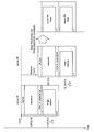
- FIG. 3 is an explanatory diagram showing a configuration example of the sensor 200 included in the system 1000 according to the present embodiment.
- the sensor 200 has, for example, a processor 250, a ROM 252, a register 254, a sensor device 256, and a communication device 258. Also, these constituent elements in the sensor 200 are connected together by, for example, an internal bus 260.
- the sensor 200 also has, for example, terminals to which external buses are connected, such as a terminal to which the data bus B1 can be connected, a terminal to which the control bus B2 can be connected, and the like, and can be connected to external buses, such as the data bus B1 and the like.
- the sensor 200 is driven by power supplied from an internal power supply (not shown), such as a battery or the like, included in the system 1000, or power supplied from a power supply external to the system 1000.
- the configuration of the sensor 200 is not limited to the example shown in FIG. 4.
- the sensor 200 may be further equipped with a recording medium for temporarily holding an image to be output.
- the recording medium for temporarily holding an image to be output include volatile memories (e.g., a random access memory (RAM), etc.), non-volatile memories (e.g., a flash memory, etc.), and the like.
- an imaging device functioning as the sensor device 256 described below is an imaging device which supports the global shutter method
- a holding capacitance for holding signal charge which is included in the imaging device can be utilized to temporarily hold an image.
- the sensor 200 includes, as the sensor device 256, an imaging device which supports the global shutter method, it is not necessary for the sensor 200 to be additionally equipped with the above recording medium for temporarily holding an image.
- the size or cost of the sensor 200 can be reduced, for example.
- the processor 250 has a function of controlling the entire sensor 200. Examples of the control performed by the processor 250 include control of recording of received control information into the register 254, control of operation of the sensor device 256, control of communication of the communication device 258, and the like.
- a process example involved in the control of recording of received control information is a “process of comparing identification information contained in the received control information with identification information 270 stored in the ROM 252, and on the basis of the result of the comparison, selectively recording the received control information into the register 254.” For example, when the identification information contained in the received control information matches the identification information 270 stored in the ROM 252, the processor 250 selectively records the received control information into the register 254.
- a process example involved in the control of operation of the sensor device 256 is a “process of transferring, to the sensor device 256, a control signal containing an instruction to operate the sensor device 256 when receiving the control information containing an image capturing instruction.”
- a process example involved in the control of communication of the communication device 258 is a “process of transferring a control signal containing a transmit instruction and data to be transmitted, to the communication device 258.”
- the ROM 252 is a recording medium included in the sensor 200.
- the ROM 252 stores, for example, identification information.
- the register 254 is another recording medium included in the sensor 200.
- the register 254 stores, for example, control information received through the control bus B2.
- FIG. 4 shows an example in which the control information is stored in the register 254, the control information may be stored in other recording media, such as non-volatile memories (e.g., a flash memory, etc.), magnetic recording media (e.g., a hard disk, etc.), and the like.
- non-volatile memories e.g., a flash memory, etc.
- magnetic recording media e.g., a hard disk, etc.
- the sensor device 256 is a device which generates an image.
- Examples of the sensor device 256 include imaging devices, such as a digital still camera, digital video camera, and the like, and any sensor devices that have a function of generating an image by imaging, such as an infrared sensor, range imaging sensor, and the like.
- An imaging device functioning as the sensor device 256 has, for example, a lens (not shown) of an optical system, an imaging element (not shown), a pixel array (not shown) corresponding to the imaging element (not shown), and a driver (not shown).
- the imaging element (not shown) according to the present embodiment is, for example, a complementary metal oxide semiconductor (CMOS) or charge coupled device (CCD). Also, the imaging element (not shown) according to the present embodiment may be a stacked imaging element, which includes a CMOS, and other constituent elements such as a CCD and the like which are stacked on the CMOS.
- the sensor 200 including an imaging device as the sensor device 256 can capture an image using the global shutter method or the rolling shutter method.
- the pixel array (not shown) has a configuration in which a plurality of pixel circuits are arranged in a matrix.
- the pixel circuits are each electrically connected to the driver (not shown) through a signal line.
- the pixel circuit includes, for example, a light reception element, such as a photodiode or the like, a transistor, a capacitance element, and the like.
- a light reception element such as a photodiode or the like
- a transistor a capacitance element, and the like.
- signal charge depending on incident light is accumulated, and the pixel circuit is initialized, according to a control signal transmitted from the driver (not shown) through the signal line.
- Examples of the transistor included in the pixel circuit include bipolar transistors, field-effect transistors (e.g., a thin film transistor (TFT), metal-oxide-semiconductor field effect transistor (MOSFET), etc.), and the like.
- the capacitance element included in the pixel circuit is, for example, a capacitor. Note that the capacitance element included in the pixel circuit may include a parasitic capacitance of an interconnect or the like.
- the driver (not shown) transmits a control signal to the pixel circuit to drive the pixel circuit.
- the imaging device functioning as the sensor device 256 has the above configuration, for example. Note that, needless to say, the configuration of the imaging device is not limited to the above example.
- the communication device 258 is, for example, a device for communicating with an external device through an external bus connected thereto, such as the data bus B1, the control bus B2, or the like.
- the communication device 258 is, for example, any device that can perform communication in accordance with any standard that allows for time-division multiplexing transmission of data, such as the CSI-2 standard, PCI Express, or the like.
- the sensor 200 has, for example, the configuration shown in FIG. 4 to output an image at an output timing based on control information. Note that, needless to say, the configuration of the sensor 200 is not limited to the example shown in FIG. 4.
- the processes in the sensor 200 involved with outputting of an image on the basis of control information will be more specifically described.
- the sensor 200 performs, as the processes involved with outputting of an image on the basis of control information, one or both of an output process according to a first example described below in (I) and an output process according to a second example described below in (II), for example.
- the processes in the sensor 200 involved with outputting of an image on the basis of control information is, for example, performed by the processor 250 included in the sensor 200 looking up control information 272 stored in the register 254.
- control information contains data (first output information) indicating amount of delay in output of image
- the sensor 200 outputs an image after a delay of the delay amount indicated by the data indicating the delay amount.
- the delay in output of an image is achieved by holding the image in the above “recording medium for temporarily holding an image,” or the above “holding capacitance included in an imaging device supporting the global shutter method which functions as the sensor device 256.”
- the sensor 200 when the data indicating a delay amount is data which directly indicates the delay amount, the sensor 200 outputs an image after a period of time corresponding to the delay amount indicated by the data indicating the delay amount has elapsed since a predetermined point of time.
- the predetermined point of time is, for example, a point of time when an image capture command or a synchronization signal is received, a point of time when exposure in imaging is ended, or the like.
- the data indicating the predetermined point of time may be previously stored in the ROM 252 or the like, or may be stored in the control information.
- the sensor 200 specifies the delay amount on the basis of the data indicating the delay amount. For example, when the data which indirectly indicates a delay amount indicates an ID associated with the delay amount, the sensor 200 specifies the delay amount by looking up it in a table (or a database) in which IDs and delay amounts are associated with each other, the table being stored in a recording medium, such as the ROM 252 or the like. Thereafter, the sensor 200 outputs an image after a period of time corresponding to the specified delay amount has elapsed since the predetermined point of time.
- the sensor 200 when only the output process according to the first example is performed, the sensor 200 outputs packets of an image at set output intervals, for example.
- the sensor 200 specifies the set output interval by looking up data indicating the output interval which is stored in a recording medium, such as the ROM 252 or the like.
- control information contains data (second output information) indicating output interval between packets which is used when image is output
- control information contains data indicating an output interval between packets
- the sensor 200 outputs packets of an image at the output intervals indicted by the data indicating the output interval between packets.
- the sensor 200 when the data indicating an output interval between packets is data which directly indicates the output interval, the sensor 200 outputs one packet, and thereafter, outputs the next packet after a period of time corresponding to the output interval indicated by the data indicating the output interval between packets has elapsed.
- the sensor 200 specifies the output interval on the basis of the data indicating the output interval between packets. For example, when the data indirectly indicating an output interval indicates an ID associated with the output interval, the sensor 200 specifies the output interval by looking up it in a table (or a database) in which IDs and output intervals are associated with each other, the table being stored in a recording medium, such as the ROM 252 or the like. The sensor 200 outputs one packet, and thereafter, outputs the next packet after a period of time corresponding to the specified output interval has elapsed.
- a table or a database
- the sensor 200 when only the output process according to the second example is performed, the sensor 200 outputs an image after a delay of a set delay amount, for example.
- the sensor 200 specifies the set delay amount by looking up data indicating the delay amount which is stored in a recording medium, such as the ROM 252 or the like, for example.
- the sensor 200 performs one or both of the output process according to the first example described above in (I) and the output process according to the second example described above in (II). Therefore, in the system 1000, images captured during a predetermined period of time are output by the sensors 200 at output timings based on the control information which is set in the sensors 200 by the processor 100. Thereafter, in the system 1000, the image output by each sensor 200 through the data bus B1 is acquired by the processor 100.
- process involved in outputting of an image according to the control information in the sensor 200 according to the present embodiment is not limited to the output process according to the first example described above in (I) or the output process according to the second example described above in (II).
- the sensor 200 when the control information contains data indicating an image size, the sensor 200 outputs an image having the image size indicated by the control information.
- control information contains data indicating a frame rate
- the sensor 200 outputs an image at the frame rate indicated by the control information.
- control information contains data indicating an image size and data indicating a frame rate
- the sensor 200 outputs an image having the image size indicated by the control information at the frame rate indicated by the control information.
- the memory 300 is a recording medium included in the system 1000.
- Examples of the memory 300 include volatile memories (e.g., RAM, etc.), non-volatile memories (e.g., a flash memory, etc.), and the like.
- the memory 300 stores an image output by each sensor 200, for example.
- the recording of an image into the memory 300 is controlled by, for example, the processor 100.
- Display device 400 is a display device included in the system 1000.
- Examples of the display device 400 include a liquid crystal display, organic electro-luminescence (EL) display, organic light emitting diode (OLED) display, and the like.
- the display screen of the display device 400 displays various images and screens, such as, for example, an image output by each sensor 200, a screen involved with an application executed by the processor 100, a screen involved with user interface (UI), and the like.
- the display of an image or the like on the display screen of the display device 400 is controlled by, for example, the processor 100.
- system 1000 has, for example, the configuration shown in FIG. 1.
- the processor 100 and the plurality of sensors 200 are connected together by the data bus B1. Also, in the system 1000, the output of an image performed by the plurality of sensors 200 is controlled by the processor 100 performing the image output control. Therefore, in the system 1000, images captured during a predetermined period of time which are independently output by the plurality of sensors 200 connected to the data bus B1 are transmitted by time-division multiplexing on the data bus B1. Thereafter, the processor 100 can receive the images independently output by the plurality of sensors 200 through the data bus B1.
- the system 1000 provides, for example, a “mechanism which performs time-division multiplexing, on the same data bus B1, with respect to images independently output by a plurality of sensors 200 which perform image capture at synchronized timings (an example in which the plurality of sensors 200 perform image capture during a predetermined period of time)”.
- the processor 100 and the plurality of sensors 200 are connected together by the data bus B1. Therefore, compared to a case where an existing standard such as the CSI-2 standard is simply utilized, the number of data buses connected to the processor 100 can be reduced.
- the reduction in the number of data buses connected to the processor 100 results in the following effects.
- a wiring region where the processor 100 and the plurality of sensors 200 are connected together can be reduced.
- the hardware configuration of the processor 100 can be further simplified due to, for example, a reduction in the number of terminals for connecting the data buses.
- the system according to the present embodiment may not have the memory 300 shown in FIG. 1.
- system according to the present embodiment can have a configuration which does not have the display device 400 shown in FIG. 1.
- system according to the present embodiment may have any configuration that is suitable for a function possessed by an electronic apparatus (described below) to which the system according to the present embodiment is applied.
- the system according to the present embodiment may have a configuration in which M data buses (where M is an integer smaller than the number of the sensors 200) are connected to the processor. Even when the system according to the present embodiment has a configuration in which M data buses (where M is an integer smaller than the number of the sensors 200 included in the system) are connected to the processor, the number of the data buses connected to the processor can be reduced, compared to when an existing standard such as the CSI-2 standard or the like is simply employed.
- a system has been described as the present embodiment by way of example.
- the present embodiment is not limited to this.
- the present embodiment is applicable to various electronic apparatuses, such as communication apparatuses (e.g., a smartphone, etc.), mobile apparatuses (e.g., a drone (an apparatus which can be remotely operated or autonomously operate), automobile, etc.), computers (e.g., a personal computer (PC), etc.), tablet-type apparatuses, game apparatuses, and the like.
- communication apparatuses e.g., a smartphone, etc.
- mobile apparatuses e.g., a drone (an apparatus which can be remotely operated or autonomously operate
- automobile etc.
- computers e.g., a personal computer (PC), etc.
- tablet-type apparatuses e.g., game apparatuses, and the like.
- a processor has been described as a processing apparatus included in the system according to the present embodiment by way of example.
- the processing apparatus according to the present embodiment is not limited to the above example.
- the processing apparatus according to the present embodiment is applicable to any processing circuit or device that can perform the output control of an image which is output by each of a plurality of image sensors connected to a data bus, through the data bus.
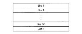
- FIG. 5 shows an example of data of an image captured by the sensor 200 included in the system 1000 according to the present embodiment.
- the data of the image captured by the sensor 200 includes N lines of data (where N is an integer of 1 or more), and is output to the data bus B1 on a line-by-line basis.
- FIG. 6 shows an example of a packet sequence of image data which is transmitted through the data bus B1 included in the system 1000 according to the present embodiment, in accordance with the CSI-2 standard.
- FS indicates a frame start (FS) packet
- FE indicates a frame end (FE) packet under the CSI-2 standard.
- PH indicates a packet header
- PF indicates a packet footer.
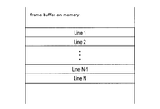
- FIG. 7 shows an example of a frame buffer which is allocated in the memory 300 included in the system 1000 according to the present embodiment.
- the processor 100 when receiving the packet sequence shown in FIG. 6, records the received image data into the frame buffer of the memory 300 as shown in FIG. 7.
- the packet sequence of image data shown in FIG. 6 is transmitted on the data bus B1, and the image data received by the processor 100 is recorded into the frame buffer as shown in FIG. 7.
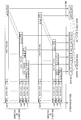
- FIG. 8 is an explanatory diagram showing an example of an operation of a sensor equipped with an imaging device which supports the rolling shutter method.
- FIG. 8 shows an operation of a sensor equipped with an imaging device which supports the rolling shutter method (may hereinafter be referred to as a “sensor supporting the rolling shutter method”) where a line N of an image is captured, and image data corresponding to the line N is output.
- pixel RST indicates resetting of pixels.
- pixel RD indicates reading of charge accumulated depending on incident light.
- AD conversion indicates conversion of an analog signal depending on read charge into a digital signal by an analog-to-digital conversion circuit (not shown).
- a sensor supporting the rolling shutter method resets pixels corresponding to the line N (pixel RST shown in FIG. 8).
- the pixel resetting corresponds to an operation of opening the shutter of the imaging device.
- signal charge depending on light entering a pixel is accumulated (accumulation shown in FIG. 8), and thereafter, the accumulated charge is read out (pixel RD shown in FIG. 8).
- the reading of the accumulated charge corresponds to an operation of closing the shutter of the imaging device.
- the read charge is analog-to-digital converted (AD conversion shown in FIG. 8) to obtain digital data corresponding to the line N, and the digital data is output to the data bus (data output shown in FIG. 8).
- FIG. 9 is an explanatory diagram showing an example of an operation of a sensor equipped with an imaging device supporting the rolling shutter method.
- the operation for a line N shown in FIG. 8 is successively performed for a plurality of lines, a line 1 to a line N (in FIG. 9, N is an integer of 4 or more).
- a series of operations i.e., pixel resetting (pixel RST shown in FIG. 9) to data output (data output shown in FIG. 9) are performed for each line at a respective different timing in order to avoid a collision between digital data corresponding to lines which is output to the data bus.
- FIG. 10 is an explanatory diagram showing an example of operations of two sensors each equipped with an imaging device supporting the rolling shutter method.
- FIG. 10 shows an example of a case where the operation shown in FIG. 9 is performed in each of the two sensors (a sensor #1 and a sensor #2) supporting the rolling shutter method so that time-division multiplexing is performed with respect to image data on the data bus.
- the two sensors supporting the rolling shutter method In order to prevent the two sensors supporting the rolling shutter method to output data to the data bus at the same timing, it is necessary to cause the two sensors supporting the rolling shutter method to capture images at different timings as shown in FIG. 2. Therefore, in the example shown in FIG. 10, after one sensor outputs data corresponding to all lines to the data bus, the other sensor outputs data corresponding to all lines to the data bus. Therefore, in the example shown in FIG. 10, the two sensors supporting the rolling shutter method do not capture images at the same time (or captured images are not regarded as being captured at the same time).
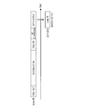
- FIG. 11 is an explanatory diagram showing an example of an operation of a sensor equipped with an imaging device supporting the global shutter method.
- FIG. 11 shows an operation of a sensor equipped with an imaging device supporting the global shutter method (may hereinafter be referred to as a “sensor supporting the global shutter method”) where a line N of an image is captured, and image data corresponding to the line N is output.
- the sensor supporting the global shutter method resets pixels corresponding to the line N (pixel RST shown in FIG. 11).
- the read charge is transferred to, for example, a capacitance element adjacent to the pixel, and is held by the capacitance element (capacitance holding of FIG. 11), unlike the sensor supporting the rolling shutter method.
- a capacitance element which holds read charge such as the above capacitance element adjacent to the pixel, is referred to as a “holding capacitance.”
- the charge held by the holding capacitance is analog-to-digital converted (AD conversion shown in FIG. 11) to obtain digital data corresponding to the line N, and the digital data is output to the data bus (data output shown in FIG. 11).
- AD conversion shown in FIG. 11 analog-to-digital converted
- the analog-to-digital conversion and the output of data to the data bus can be delayed by the holding capacitance holding charge.
- FIG. 12 is an explanatory diagram showing an example of an operation of a sensor equipped with an imaging device supporting the global shutter method where the operation for a line N shown in FIG. 12 is successively performed for a plurality of lines, a line 1 to a line N (in FIG. 12, N is an integer of 4 or more).
- pixel resetting (pixel RST shown in FIG. 12) can be started for all lines simultaneously. Also, for example, as shown in FIG. 12, in the sensor supporting the global shutter method, the accumulation of signal charge (accumulation shown in FIG. 12) and the reading of accumulated charge (pixel RD shown in FIG. 12) are performed for all lines simultaneously. Note that, in the sensor supporting the global shutter method, the accumulation of signal charge (accumulation shown in FIG. 12) and the reading of accumulated charge (pixel RD shown in FIG. 12) can be changed on a line-by-line basis.
- the sensor supporting the global shutter method transfers charge read from each line to the holding capacitance so that the charge is held by the holding capacitance (capacitance holding shown in FIG. 12), analog-to-digital converts the charge held in the holding capacitance successively on a line-by-line basis, and outputs the data to the data bus (AD conversion and data output shown in FIG. 12).
- FIG. 12 does not show that, in the line 1 (line 1 shown in FIG. 12), read charge is transferred to the holding capacitance, and is held by the holding capacitance (note that this is not shown in FIG. 13 and FIG. 14 described below, as in FIG. 12).
- the sensor device 256 included in the sensor 200 included in the system 1000 is a sensor supporting the global shutter method, and temporarily holds an image using a holding capacitance
- the sensor 200 may not be equipped with a recording medium for temporarily holding an image, such as a RAM or the like.
- the sensor 200 can be equipped with a recording medium for temporarily holding an image, such as a RAM or the like, so that the sensor 200 can also temporarily hold an image.
- FIG. 13 is an explanatory diagram showing a first example of output of an image performed by the sensor 200 in the system 1000 according to the present embodiment.
- FIG. 13 shows an example of operations of the sensors 200A and 200B, each of which includes a sensor supporting the global shutter method as the sensor device 256.
- the sensor 200A and the sensor 200B synchronously operate through the control bus B2, for example.
- pixels are reset (pixel RST shown in FIG. 13) synchronously on the basis of reception of the synchronization signal Vsync, and thereafter, signal charge is accumulated (accumulation shown in FIG. 13), and the accumulated charge is read out (pixel RD shown in FIG. 13), for example.
- the sensors 200A and 200B each transfer charge read from each line to the holding capacitance so that the charge is held by the holding capacitance (capacitance holding shown in FIG. 13), analog-to-digital convert the charge held by the holding capacitance on a line-by-line basis, and output data to the data bus B1 (AD conversion and data output shown in FIG. 13).
- the sensors 200A and 200B each output an image at an output timing based on the control information stored in the register 254, for example.
- the sensors 200A and 200B each hold the charge read from each line in the holding capacitance so that output is delayed by the delay amount corresponding to the data indicating the delay amount.
- the sensors 200A and 200B each output data corresponding to each line to the data bus B1 at the output intervals indicated by the data indicating the output interval.
- a delay amount indicated by the control information stored in the register 254 included in the sensor 200B is larger than a delay amount indicated by the control information stored in the register 254 included in the sensor 200A. More specifically, in the example shown in FIG. 13, the control information according to which, after the sensor 200A outputs data corresponding to all lines to the data bus B1, the sensor 200B outputs data corresponding to each line, is stored in the register 254 of each of the sensors 200A and 200B.
- the intervals at which the sensor 200A outputs data corresponding to each line are the same as the intervals at which the sensor 200B outputs data corresponding to each line.
- the intervals at which the sensors 200A and 200B each output data are not limited to the example shown in FIG. 13.
- the sensors 200A and 200B may each output data corresponding to each line to the data bus B1 at output intervals indicated by the control information so that the data output interval of the sensor 200A is different from the data output interval of the sensor 200B.
- the sensors 200A and 200B can each output an image at an output timing based on the control information so that images having the same image capture timing (images captured during a predetermined period of time) between the sensors 200A and 200B are transmitted by time-division multiplexing on the data bus B1.
- FIG. 14 is an explanatory diagram showing a second example of output of an image performed by the sensor 200 in the system 1000 according to the present embodiment.
- FIG. 14 shows another example of operations of the sensors 200A and 200B each equipped with a sensor supporting the global shutter method as the sensor device 256.
- the sensor 200A and the sensor 200B operate synchronously through the control bus B2, for example.
- each of the sensors 200A and 200B shown in FIG. 14 is the same as the operation of each of the sensors 200A and 200B in the first output example shown in FIG. 13.
- the control information which is looked up by each of the sensors 200A and 200B is different from that in the example shown in FIG. 13, and there is a difference in the order in which image data is output, between the second output example shown in FIG. 14 and the first output example shown in FIG. 13.
- a delay amount indicated by the control information stored in the register 254 included in the sensor 200B is larger than a delay amount indicated by the control information stored in the register 254 included in the sensor 200A. More specifically, in the example shown in FIG. 14, the control information according to which the output of data corresponding to each line to the data bus B1 performed by the sensor 200A, and the output of data corresponding to each line to the data bus B1 performed by the sensor 200B, are alternately performed, is stored in the register 254 of each of the sensors 200A and 200B.
- the intervals at which the sensor 200A outputs data corresponding to each line are the same as the intervals at which the sensor 200B outputs data corresponding to each line.
- the intervals at which the sensors 200A and 200B each output data are not limited to the example shown in FIG. 14.
- the sensors 200A and 200B may each output data corresponding to each line to the data bus B1 at output intervals indicated by the control information so that the data output interval of the sensor 200A and the data output interval of the sensor 200A are different from each other (within a range which does not cause data collision on the data bus B1).
- the sensors 200A and 200B can each output an image at an output timing based on the control information so that images having the same image capture timing (images captured during a predetermined period of time) between the sensors 200A and 200B are transmitted by time-division multiplexing on the data bus B1.
- each sensor 200 can output an image at an output timing based on the control information so that images output by the sensors 200 are transmitted by time-division multiplexing on the data bus B1, as in the first output example and the second output example.
- the sensors 200 may be equipped with a recording medium, such as a RAM or the like, for temporarily holding an image, and hold data corresponding to each line obtained by analog-to-digital conversion in the recording medium, whereby the timing of output of data to the data bus B1 by each sensor 200 is adjusted.
- a recording medium such as a RAM or the like
- each sensor 200 can output an image at an output timing based on control information so that images output by the sensors 200 can be transmitted by time-division multiplexing on the data bus B1, as in the first output example and the second output example.
- the sensors 200 can be equipped with a sensor supporting the global shutter method, or a sensor device other than the sensor supporting the global shutter method, such as the above sensor supporting the rolling shutter method or the like, as the sensor device 256, for example.
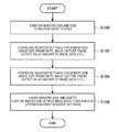
- FIG. 15 is a flowchart showing an example of a process involved in control of output of an image performed by the processor 100 included in the system 1000 according to the present embodiment (a process involved in the control method according to according to the present embodiment).
- FIG. 15 shows an example of a process involved in control of output of an image performed by the processor 100 in a case where the system 1000 has two image sensors 200A and 200B.
- the processor 100 turns on each of the sensors 200A and 200B to be controlled, and thereby releases their reset status (S100).
- the process of step S100 corresponds to an example of a process of initializing the sensors 200A and 200B, for example.
- the processor 100 configures register settings for the sensor 200A (S102).
- the processor 100 configures the register settings for the sensor 200A by transmitting control information through the control bus B2.
- the processor 100 configures the register settings for the sensor 200A by transmitting control information in which, for example, the sensor 200A is designated, and the address of a register included in the sensor 200A is designated.
- the processor 100 can configure the register settings for the sensor 200A by transmitting control information in which all sensors 200 to be controlled are designated, and the address of a register included in each sensor 200 is designated, for example.
- the transmission of the control information in which all sensors 200 to be controlled are designated, and the address of a register included in each sensor 200 is designated, is effective in synchronously recording the same data into the registers included in all of the sensors 200, for example.
- the processor 100 configures register settings for the sensor 200B (S104). As in step S102, the processor 100 configures the register settings for the sensor 200B by transmitting control information through the control bus B2.
- the processor 100 causes each of the sensors 200A and 200B to capture an image and output image data to the data bus B1 (S106).
- the processor 100 transmits control information through the control bus B2 to cause each of the sensors 200A and 200B to capture an image and output image data to the data bus B1.
- the processor 100 performs, for example, the process shown in FIG. 15 as a process involved in the image output control. Note that, needless to say, the example of a process involved in the image output control is not limited to the example shown in FIG. 15.
- control information is recorded into the register included in the sensor 200 by the processor 100 controlling output of an image as shown in FIG. 15. Also, as described above, the sensor 200 outputs an image at an output timing based on the control information.
- a program or the like for causing a computer to function as the processing apparatus according to the present embodiment e.g., a program for causing a computer to perform a process involved in the image output control (a process involved in the control method according to according to the present embodiment)
- a “mechanism which performs time-division multiplexing, on the same data bus B1, with respect to images independently output by a plurality of image sensors 200 which perform image capture at synchronized timings (an example in which the plurality of sensors 200 perform image capture during a predetermined period of time)” can be provided, for example.
- effects exhibited by the above process involved in output control of an image can be exhibited by a program for causing a computer to function as the processing apparatus according to the present embodiment being executed by a processor or the like in the computer.
- a program for causing a computer to function as the processing apparatus according to the present embodiment is provided.
- a recording medium storing the above program can be additionally provided.
- a processing apparatus including: a processing unit that is connectable to a data bus, and performs output control on respective images captured by a plurality of image sensors connected to the data bus during a predetermined period of time, wherein a timing of output of the image performed by each of the plurality of image sensors is changed by the output control.
- the processing unit controls, as the output control, a delay when the image sensor outputs the image.
- the processing unit controls, as the output control, output intervals at which packets are output when the image sensor outputs the image.
- An image sensor that is connectable to a data bus to which another image sensor is connected, and outputs an image captured during a predetermined period of time, at an output timing based on control information.
- the control information contains first output information indicating a delay amount when an image is output , and the image is output after a delay of the delay amount indicated by the first output information.
- the control information contains second output information indicating output intervals at which packets are output when an image is output, and the packets of the image are output at the output intervals indicated by the second output information.
- the control information is stored in a register.
- a system including: a plurality of image sensors that are connected to a data bus, and a processing apparatus that is connected to the data bus, wherein the processing apparatus includes a processing unit that performs output control on respective images captured by the plurality of image sensors during a predetermined period of time, and a timing of output of the image in each of the plurality of image sensors is changed by the output control.
Landscapes
- Engineering & Computer Science (AREA)
- Multimedia (AREA)
- Signal Processing (AREA)
- Studio Devices (AREA)
- Image Processing (AREA)
- Bus Control (AREA)
Priority Applications (4)
| Application Number | Priority Date | Filing Date | Title |
|---|---|---|---|
| US16/094,350 US11252305B2 (en) | 2016-05-27 | 2017-04-10 | Processing apparatus, image device and system with image data via single common data bus |
| CN201780031034.9A CN109155814B (zh) | 2016-05-27 | 2017-04-10 | 处理装置、图像传感器和系统 |
| KR1020187031825A KR102343629B1 (ko) | 2016-05-27 | 2017-04-10 | 처리 장치, 화상 센서 및 시스템 |
| EP17721876.5A EP3466045B1 (en) | 2016-05-27 | 2017-04-10 | Processing apparatus, image sensor, and system |
Applications Claiming Priority (2)
| Application Number | Priority Date | Filing Date | Title |
|---|---|---|---|
| JP2016-106555 | 2016-05-27 | ||
| JP2016106555A JP6722044B2 (ja) | 2016-05-27 | 2016-05-27 | 処理装置、画像センサ、およびシステム |
Publications (1)
| Publication Number | Publication Date |
|---|---|
| WO2017203857A1 true WO2017203857A1 (en) | 2017-11-30 |
Family
ID=58671877
Family Applications (1)
| Application Number | Title | Priority Date | Filing Date |
|---|---|---|---|
| PCT/JP2017/014726 WO2017203857A1 (en) | 2016-05-27 | 2017-04-10 | Processing apparatus, image sensor, and system |
Country Status (7)
| Country | Link |
|---|---|
| US (1) | US11252305B2 (zh) |
| EP (1) | EP3466045B1 (zh) |
| JP (1) | JP6722044B2 (zh) |
| KR (1) | KR102343629B1 (zh) |
| CN (1) | CN109155814B (zh) |
| TW (1) | TWI758286B (zh) |
| WO (1) | WO2017203857A1 (zh) |
Cited By (1)
| Publication number | Priority date | Publication date | Assignee | Title |
|---|---|---|---|---|
| EP3843376A4 (en) * | 2018-08-20 | 2021-09-15 | Sony Semiconductor Solutions Corporation | IMAGE PROCESSING DEVICE, AND IMAGE PROCESSING SYSTEM |
Families Citing this family (3)
| Publication number | Priority date | Publication date | Assignee | Title |
|---|---|---|---|---|
| KR102385333B1 (ko) * | 2017-09-15 | 2022-04-12 | 삼성전자주식회사 | 복수의 이미지 센서들을 제어하기 위한 전자 장치 및 방법 |
| CN111551948B (zh) * | 2020-05-20 | 2022-08-16 | 炬佑智能科技(苏州)有限公司 | 一种tof设备的控制方法、计算机存储介质 |
| US11757995B2 (en) * | 2021-04-27 | 2023-09-12 | Stmicroelectronics S.R.L. | Sensors with enhanced time division multiplexing frames |
Citations (5)
| Publication number | Priority date | Publication date | Assignee | Title |
|---|---|---|---|---|
| US20070076112A1 (en) * | 2005-10-05 | 2007-04-05 | Hitachi, Ltd. | Stereo image-pickup apparatus |
| US20120162511A1 (en) * | 2010-12-22 | 2012-06-28 | Texas Instruments Incorporated | Multi-sensor video frame synchronization apparatus and methods |
| US20130329127A1 (en) * | 2011-03-08 | 2013-12-12 | Renesas Electronics Corporation | Image pickup apparatus |
| US20140281753A1 (en) | 2013-03-15 | 2014-09-18 | Mahesh Wagh | Systems, Apparatuses, and Methods for Handling Timeouts |
| US20150009288A1 (en) * | 2013-07-05 | 2015-01-08 | Mediatek Inc. | Synchronization controller for multi-sensor camera device and related synchronization method |
Family Cites Families (22)
| Publication number | Priority date | Publication date | Assignee | Title |
|---|---|---|---|---|
| US6590198B1 (en) * | 1998-03-16 | 2003-07-08 | Photon Vision Systems, Inc. | Video bus for high speed multi-resolution imagers |
| CA2410537A1 (en) * | 2000-06-01 | 2001-12-06 | Atmel Corporation | Dual-mode cmos integrated imager |
| US6952228B2 (en) * | 2000-10-13 | 2005-10-04 | Canon Kabushiki Kaisha | Image pickup apparatus |
| JP2004023397A (ja) * | 2002-06-14 | 2004-01-22 | Matsushita Electric Ind Co Ltd | 画像処理システム |
| CN101427372B (zh) * | 2004-08-25 | 2012-12-12 | 普罗塔里斯菲洛有限责任公司 | 用于多个相机装置的设备和操作该设备的方法 |
| US7557849B2 (en) | 2004-10-11 | 2009-07-07 | Mediatek Usa Inc | Processor-controlled timing generator for multiple image sensors |
| US20070222879A1 (en) * | 2006-03-24 | 2007-09-27 | Intel Corporation | Sub-ranging pixel sample and hold |
| EP2005214A4 (en) * | 2006-03-30 | 2012-04-18 | Given Imaging Ltd | IN VIVO DETECTION DEVICE AND METHOD FOR COMMUNICATING BETWEEN IMAGING DEVICES AND CORRESPONDING PROCESSOR |
| JP2010527457A (ja) * | 2007-04-18 | 2010-08-12 | 株式会社オプトエレクトロニクス | 移動物体を撮像するための撮像方法及び撮像装置 |
| JP5012188B2 (ja) * | 2007-05-14 | 2012-08-29 | コニカミノルタホールディングス株式会社 | 固体撮像装置 |
| US7969469B2 (en) * | 2007-11-30 | 2011-06-28 | Omnivision Technologies, Inc. | Multiple image sensor system with shared processing |
| JP5651976B2 (ja) | 2010-03-26 | 2015-01-14 | ソニー株式会社 | 固体撮像素子およびその製造方法、並びに電子機器 |
| JP5703132B2 (ja) * | 2011-05-30 | 2015-04-15 | 株式会社東芝 | 固体撮像装置 |
| EP2719166B1 (en) * | 2011-06-10 | 2018-03-28 | Flir Systems, Inc. | Line based image processing and flexible memory system |
| JP2013066132A (ja) * | 2011-09-20 | 2013-04-11 | Fuji Xerox Co Ltd | 画像読取装置、画像形成装置、及びプログラム |
| CN102447847A (zh) * | 2011-11-02 | 2012-05-09 | 北京思比科微电子技术股份有限公司 | 包含mipi接口的多图像传感器图像处理装置及方法 |
| KR101796481B1 (ko) * | 2011-11-28 | 2017-12-04 | 삼성전자주식회사 | 저전력 셔터랙 제거 방법, 카메라 모듈 및 이를 구비하는 모바일 기기 |
| US10256833B2 (en) * | 2013-01-23 | 2019-04-09 | Forza Silicon Corporation | Dual reset branch analog-to-digital conversion |
| JP6141160B2 (ja) * | 2013-09-25 | 2017-06-07 | ソニーセミコンダクタソリューションズ株式会社 | 固体撮像素子およびその動作方法、並びに電子機器およびその動作方法 |
| CN203813894U (zh) * | 2014-05-09 | 2014-09-03 | 哈尔滨水星电子科技有限公司 | 一种接口共享的全景数字图像传感器 |
| KR102618490B1 (ko) * | 2018-12-13 | 2023-12-27 | 삼성전자주식회사 | 이미지 센서 및 이의 구동 방법 |
| US11070754B1 (en) * | 2020-03-24 | 2021-07-20 | Stmicroelectronics Asia Pacific Pte Ltd. | Slew rate control circuit for an image sensor |
-
2016
- 2016-05-27 JP JP2016106555A patent/JP6722044B2/ja active Active
-
2017
- 2017-04-10 EP EP17721876.5A patent/EP3466045B1/en active Active
- 2017-04-10 CN CN201780031034.9A patent/CN109155814B/zh active Active
- 2017-04-10 WO PCT/JP2017/014726 patent/WO2017203857A1/en unknown
- 2017-04-10 KR KR1020187031825A patent/KR102343629B1/ko active IP Right Grant
- 2017-04-10 US US16/094,350 patent/US11252305B2/en active Active
- 2017-04-20 TW TW106113210A patent/TWI758286B/zh active
Patent Citations (5)
| Publication number | Priority date | Publication date | Assignee | Title |
|---|---|---|---|---|
| US20070076112A1 (en) * | 2005-10-05 | 2007-04-05 | Hitachi, Ltd. | Stereo image-pickup apparatus |
| US20120162511A1 (en) * | 2010-12-22 | 2012-06-28 | Texas Instruments Incorporated | Multi-sensor video frame synchronization apparatus and methods |
| US20130329127A1 (en) * | 2011-03-08 | 2013-12-12 | Renesas Electronics Corporation | Image pickup apparatus |
| US20140281753A1 (en) | 2013-03-15 | 2014-09-18 | Mahesh Wagh | Systems, Apparatuses, and Methods for Handling Timeouts |
| US20150009288A1 (en) * | 2013-07-05 | 2015-01-08 | Mediatek Inc. | Synchronization controller for multi-sensor camera device and related synchronization method |
Cited By (2)
| Publication number | Priority date | Publication date | Assignee | Title |
|---|---|---|---|---|
| EP3843376A4 (en) * | 2018-08-20 | 2021-09-15 | Sony Semiconductor Solutions Corporation | IMAGE PROCESSING DEVICE, AND IMAGE PROCESSING SYSTEM |
| US11647284B2 (en) | 2018-08-20 | 2023-05-09 | Sony Semiconductor Solutions Corporation | Image processing apparatus and image processing system with image combination that implements signal level matching |
Also Published As
| Publication number | Publication date |
|---|---|
| CN109155814A (zh) | 2019-01-04 |
| TWI758286B (zh) | 2022-03-21 |
| JP6722044B2 (ja) | 2020-07-15 |
| KR102343629B1 (ko) | 2021-12-28 |
| US20190124235A1 (en) | 2019-04-25 |
| KR20190013728A (ko) | 2019-02-11 |
| EP3466045A1 (en) | 2019-04-10 |
| EP3466045B1 (en) | 2024-04-03 |
| CN109155814B (zh) | 2022-01-11 |
| TW201805891A (zh) | 2018-02-16 |
| JP2017212690A (ja) | 2017-11-30 |
| US11252305B2 (en) | 2022-02-15 |
Similar Documents
| Publication | Publication Date | Title |
|---|---|---|
| US11252305B2 (en) | Processing apparatus, image device and system with image data via single common data bus | |
| KR102402716B1 (ko) | 처리 장치, 화상 센서 및 시스템 | |
| US9723239B2 (en) | Image sensor and method of outputting data from the image sensor | |
| US20140368609A1 (en) | Systems And Methods For Generating A Panoramic Image | |
| CN110326285B (zh) | 图像传感器和控制系统 | |
| KR102362138B1 (ko) | 이미지 센서 모듈 및 그것을 포함하는 이미지 센서 장치 | |
| CN108432228B (zh) | 图像数据的帧同步方法、图像信号处理单元、装置及终端 | |
| US9781369B2 (en) | Image sensor and image processing system including the same | |
| US9569160B2 (en) | Display processing device and imaging apparatus | |
| US20160248990A1 (en) | Image sensor and image processing system including same | |
| US9658815B2 (en) | Display processing device and imaging apparatus | |
| CN107544124B (zh) | 摄像设备及其控制方法和存储介质 | |
| EP3595296B1 (en) | Image sensor and transmission system |
Legal Events
| Date | Code | Title | Description |
|---|---|---|---|
| ENP | Entry into the national phase |
Ref document number: 20187031825 Country of ref document: KR Kind code of ref document: A |
|
| NENP | Non-entry into the national phase |
Ref country code: DE |
|
| 121 | Ep: the epo has been informed by wipo that ep was designated in this application |
Ref document number: 17721876 Country of ref document: EP Kind code of ref document: A1 |
|
| ENP | Entry into the national phase |
Ref document number: 2017721876 Country of ref document: EP Effective date: 20190102 |