WO2017195639A1 - ウエハレベルパッケージおよびキャパシタ - Google Patents
ウエハレベルパッケージおよびキャパシタ Download PDFInfo
- Publication number
- WO2017195639A1 WO2017195639A1 PCT/JP2017/016814 JP2017016814W WO2017195639A1 WO 2017195639 A1 WO2017195639 A1 WO 2017195639A1 JP 2017016814 W JP2017016814 W JP 2017016814W WO 2017195639 A1 WO2017195639 A1 WO 2017195639A1
- Authority
- WO
- WIPO (PCT)
- Prior art keywords
- capacitor
- layer
- wafer level
- level package
- chip
- Prior art date
- Legal status (The legal status is an assumption and is not a legal conclusion. Google has not performed a legal analysis and makes no representation as to the accuracy of the status listed.)
- Ceased
Links
Images







Classifications
-
- H—ELECTRICITY
- H10—SEMICONDUCTOR DEVICES; ELECTRIC SOLID-STATE DEVICES NOT OTHERWISE PROVIDED FOR
- H10D—INORGANIC ELECTRIC SEMICONDUCTOR DEVICES
- H10D1/00—Resistors, capacitors or inductors
- H10D1/60—Capacitors
- H10D1/68—Capacitors having no potential barriers
-
- H—ELECTRICITY
- H01—ELECTRIC ELEMENTS
- H01G—CAPACITORS; CAPACITORS, RECTIFIERS, DETECTORS, SWITCHING DEVICES, LIGHT-SENSITIVE OR TEMPERATURE-SENSITIVE DEVICES OF THE ELECTROLYTIC TYPE
- H01G4/00—Fixed capacitors; Processes of their manufacture
- H01G4/002—Details
- H01G4/224—Housing; Encapsulation
-
- H—ELECTRICITY
- H01—ELECTRIC ELEMENTS
- H01G—CAPACITORS; CAPACITORS, RECTIFIERS, DETECTORS, SWITCHING DEVICES, LIGHT-SENSITIVE OR TEMPERATURE-SENSITIVE DEVICES OF THE ELECTROLYTIC TYPE
- H01G4/00—Fixed capacitors; Processes of their manufacture
- H01G4/33—Thin- or thick-film capacitors (thin- or thick-film circuits; capacitors without a potential-jump or surface barrier specially adapted for integrated circuits, details thereof, multistep manufacturing processes therefor)
-
- H—ELECTRICITY
- H10—SEMICONDUCTOR DEVICES; ELECTRIC SOLID-STATE DEVICES NOT OTHERWISE PROVIDED FOR
- H10W—GENERIC PACKAGES, INTERCONNECTIONS, CONNECTORS OR OTHER CONSTRUCTIONAL DETAILS OF DEVICES COVERED BY CLASS H10
- H10W20/00—Interconnections in chips, wafers or substrates
- H10W20/20—Interconnections within wafers or substrates, e.g. through-silicon vias [TSV]
-
- H—ELECTRICITY
- H10—SEMICONDUCTOR DEVICES; ELECTRIC SOLID-STATE DEVICES NOT OTHERWISE PROVIDED FOR
- H10W—GENERIC PACKAGES, INTERCONNECTIONS, CONNECTORS OR OTHER CONSTRUCTIONAL DETAILS OF DEVICES COVERED BY CLASS H10
- H10W20/00—Interconnections in chips, wafers or substrates
- H10W20/40—Interconnections external to wafers or substrates, e.g. back-end-of-line [BEOL] metallisations or vias connecting to gate electrodes
- H10W20/49—Adaptable interconnections, e.g. fuses or antifuses
-
- H—ELECTRICITY
- H10—SEMICONDUCTOR DEVICES; ELECTRIC SOLID-STATE DEVICES NOT OTHERWISE PROVIDED FOR
- H10W—GENERIC PACKAGES, INTERCONNECTIONS, CONNECTORS OR OTHER CONSTRUCTIONAL DETAILS OF DEVICES COVERED BY CLASS H10
- H10W20/00—Interconnections in chips, wafers or substrates
- H10W20/40—Interconnections external to wafers or substrates, e.g. back-end-of-line [BEOL] metallisations or vias connecting to gate electrodes
- H10W20/495—Capacitive arrangements or effects of, or between wiring layers
- H10W20/496—Capacitor integral with wiring layers
-
- H—ELECTRICITY
- H10—SEMICONDUCTOR DEVICES; ELECTRIC SOLID-STATE DEVICES NOT OTHERWISE PROVIDED FOR
- H10W—GENERIC PACKAGES, INTERCONNECTIONS, CONNECTORS OR OTHER CONSTRUCTIONAL DETAILS OF DEVICES COVERED BY CLASS H10
- H10W70/00—Package substrates; Interposers; Redistribution layers [RDL]
- H10W70/60—Insulating or insulated package substrates; Interposers; Redistribution layers
-
- H—ELECTRICITY
- H10—SEMICONDUCTOR DEVICES; ELECTRIC SOLID-STATE DEVICES NOT OTHERWISE PROVIDED FOR
- H10W—GENERIC PACKAGES, INTERCONNECTIONS, CONNECTORS OR OTHER CONSTRUCTIONAL DETAILS OF DEVICES COVERED BY CLASS H10
- H10W74/00—Encapsulations, e.g. protective coatings
- H10W74/01—Manufacture or treatment
- H10W74/019—Manufacture or treatment using temporary auxiliary substrates
-
- H—ELECTRICITY
- H10—SEMICONDUCTOR DEVICES; ELECTRIC SOLID-STATE DEVICES NOT OTHERWISE PROVIDED FOR
- H10W—GENERIC PACKAGES, INTERCONNECTIONS, CONNECTORS OR OTHER CONSTRUCTIONAL DETAILS OF DEVICES COVERED BY CLASS H10
- H10W90/00—Package configurations
- H10W90/701—Package configurations characterised by the relative positions of pads or connectors relative to package parts
-
- H—ELECTRICITY
- H01—ELECTRIC ELEMENTS
- H01G—CAPACITORS; CAPACITORS, RECTIFIERS, DETECTORS, SWITCHING DEVICES, LIGHT-SENSITIVE OR TEMPERATURE-SENSITIVE DEVICES OF THE ELECTROLYTIC TYPE
- H01G4/00—Fixed capacitors; Processes of their manufacture
- H01G4/002—Details
- H01G4/018—Dielectrics
- H01G4/06—Solid dielectrics
- H01G4/08—Inorganic dielectrics
- H01G4/12—Ceramic dielectrics
-
- H—ELECTRICITY
- H10—SEMICONDUCTOR DEVICES; ELECTRIC SOLID-STATE DEVICES NOT OTHERWISE PROVIDED FOR
- H10W—GENERIC PACKAGES, INTERCONNECTIONS, CONNECTORS OR OTHER CONSTRUCTIONAL DETAILS OF DEVICES COVERED BY CLASS H10
- H10W70/00—Package substrates; Interposers; Redistribution layers [RDL]
- H10W70/01—Manufacture or treatment
- H10W70/05—Manufacture or treatment of insulating or insulated package substrates, or of interposers, or of redistribution layers
- H10W70/08—Manufacture or treatment of insulating or insulated package substrates, or of interposers, or of redistribution layers by depositing layers on the chip or wafer, e.g. "chip-first" RDLs
- H10W70/09—Manufacture or treatment of insulating or insulated package substrates, or of interposers, or of redistribution layers by depositing layers on the chip or wafer, e.g. "chip-first" RDLs extending onto an encapsulation that laterally surrounds the chip or wafer, e.g. fan-out wafer level package [FOWLP] RDLs
-
- H—ELECTRICITY
- H10—SEMICONDUCTOR DEVICES; ELECTRIC SOLID-STATE DEVICES NOT OTHERWISE PROVIDED FOR
- H10W—GENERIC PACKAGES, INTERCONNECTIONS, CONNECTORS OR OTHER CONSTRUCTIONAL DETAILS OF DEVICES COVERED BY CLASS H10
- H10W70/00—Package substrates; Interposers; Redistribution layers [RDL]
- H10W70/60—Insulating or insulated package substrates; Interposers; Redistribution layers
- H10W70/62—Insulating or insulated package substrates; Interposers; Redistribution layers characterised by their interconnections
- H10W70/65—Shapes or dispositions of interconnections
- H10W70/654—Top-view layouts
- H10W70/656—Fan-in layouts
-
- H—ELECTRICITY
- H10—SEMICONDUCTOR DEVICES; ELECTRIC SOLID-STATE DEVICES NOT OTHERWISE PROVIDED FOR
- H10W—GENERIC PACKAGES, INTERCONNECTIONS, CONNECTORS OR OTHER CONSTRUCTIONAL DETAILS OF DEVICES COVERED BY CLASS H10
- H10W72/00—Interconnections or connectors in packages
- H10W72/20—Bump connectors, e.g. solder bumps or copper pillars; Dummy bumps; Thermal bumps
- H10W72/241—Dispositions, e.g. layouts
-
- H—ELECTRICITY
- H10—SEMICONDUCTOR DEVICES; ELECTRIC SOLID-STATE DEVICES NOT OTHERWISE PROVIDED FOR
- H10W—GENERIC PACKAGES, INTERCONNECTIONS, CONNECTORS OR OTHER CONSTRUCTIONAL DETAILS OF DEVICES COVERED BY CLASS H10
- H10W72/00—Interconnections or connectors in packages
- H10W72/90—Bond pads, in general
- H10W72/941—Dispositions of bond pads
- H10W72/9413—Dispositions of bond pads on encapsulations
-
- H—ELECTRICITY
- H10—SEMICONDUCTOR DEVICES; ELECTRIC SOLID-STATE DEVICES NOT OTHERWISE PROVIDED FOR
- H10W—GENERIC PACKAGES, INTERCONNECTIONS, CONNECTORS OR OTHER CONSTRUCTIONAL DETAILS OF DEVICES COVERED BY CLASS H10
- H10W74/00—Encapsulations, e.g. protective coatings
- H10W74/10—Encapsulations, e.g. protective coatings characterised by their shape or disposition
- H10W74/111—Encapsulations, e.g. protective coatings characterised by their shape or disposition the semiconductor body being completely enclosed
- H10W74/129—Encapsulations, e.g. protective coatings characterised by their shape or disposition the semiconductor body being completely enclosed forming a chip-scale package [CSP]
Definitions
- the present invention relates to a wafer level package, and more particularly to a wafer level package in which a capacitor is built in a rewiring layer.
- a method of packaging an electronic component, particularly an IC chip, and mounting it on a substrate as a package is known.
- a wafer level package (hereinafter also referred to as “WLP”) is known (Patent Document 1).
- a typical WLP 101 includes a semiconductor substrate (IC chip) 102, a resin layer 103 provided so as to cover the IC chip 102, and rewiring inside the IC chip 102 and the resin layer 103.
- a rewiring layer 106 having a wiring 104 and a via 105, a connection pad 107 exposed from the rewiring layer 106, and a solder ball 108 provided on the connection pad 107.
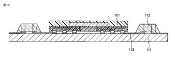
- the WLP 101 as described above is mounted on the circuit board 111 as shown in FIG.
- the present inventors connect the capacitor chip and the IC chip to the wiring 113 on the circuit board 111 when other components such as the capacitor chip 112 are present on the circuit board 111. Therefore, the wiring between the capacitor chip and the IC chip becomes long, the parasitic inductance due to this wiring becomes relatively large, and the electrical characteristics deteriorate. It has been found that there is a problem that the function of suppressing, the function of absorbing high-frequency ripple, etc. are reduced. Moreover, since the capacitor chip occupies a certain area of the circuit board, there is also a problem that it is disadvantageous for miniaturization.
- an object of the present invention is to provide an element that can reduce the wiring length between an IC chip and a capacitor as much as possible in a circuit having an IC chip and a capacitor, and is advantageous for further miniaturization.
- the present inventors can shorten the wiring length between the IC chip and the capacitor by mounting the capacitor in the wafer level package rather than mounting it on the circuit board. Furthermore, it has been found that a wafer level package advantageous for miniaturization of a circuit board can be obtained.
- an IC chip According to a first aspect of the present invention, an IC chip; A rewiring layer provided on the IC chip; A capacitor built in the redistribution layer; There is provided a wafer level package comprising:
- an electronic device including a circuit board on which the wafer level package is mounted.
- a capacitor comprising a conductive porous substrate, a dielectric layer positioned on the conductive porous substrate, and an upper electrode positioned on the dielectric layer.
- a capacitor is provided in which the outermost layer on at least one main surface of the capacitor is a solder plating layer or a metal nanoparticle layer.
- the capacitor in the wafer level package, the electrical characteristics are improved and further miniaturization is facilitated.
- FIG. 1 is a schematic cross-sectional view of a wafer level package 1a according to an embodiment of the present invention.
- FIG. 2 is a schematic cross-sectional view of the capacitor 21 used in the wafer level package of the present invention.
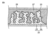
- FIG. 3 schematically shows a cross section of the porous portion of the capacitor 21 of FIG.
- FIG. 4 is a schematic sectional view of the capacitor 31 used in the wafer level package of the present invention.
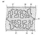
- FIG. 5 schematically shows a cross section of the porous portion of the capacitor 31 of FIG.
- FIG. 6A is a diagram for explaining a method of manufacturing the wafer level package 1a shown in FIG.
- FIG. 6B is a diagram for explaining a method of manufacturing the wafer level package 1a shown in FIG. FIG.
- FIG. 7 is a schematic cross-sectional view of a wafer level package 1b according to another embodiment of the present invention.
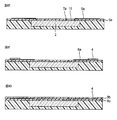
- FIG. 8-1 is a diagram for explaining a method of manufacturing the wafer level package 1b shown in FIG.
- FIG. 8-2 is a diagram for explaining a method of manufacturing the wafer level package 1b shown in FIG. 8-3 is a diagram for explaining a method of manufacturing the wafer level package 1b shown in FIG.
- FIG. 9 is a schematic sectional view of a conventional wafer level package 101.
- FIG. 10 is a schematic cross-sectional view of a circuit board 111 on which a conventional wafer level package 101 is mounted.
- FIG. 1 A schematic cross-sectional view of a wafer level package 1a according to an embodiment of the present invention is shown in FIG.
- the wafer level package 1 a of the present embodiment is schematically incorporated in the IC chip 2, the rewiring layer 3 provided on the IC chip 2, and the rewiring layer 3.
- the capacitor 4 and the solder ball 5 provided on the rewiring layer 3 are included.
- the rewiring layer 3 includes wiring 6, vias 7, and connection pads 8.
- the electrodes of the IC chip 2 are electrically connected to the solder balls 5 via wirings 6, vias 7, and connection pads 8 provided in the rewiring layer 3 (partially via capacitors 4). ing.
- the IC (integrated circuit) chip may be a semiconductor substrate itself in which a circuit including a transistor or the like is formed on one surface of a Si substrate or a GaAs substrate, or may be an element including the semiconductor substrate.
- the IC chip is a semiconductor substrate itself having a circuit formed on one surface.
- the IC chip has two main surfaces.
- the main surface on which an electrode (ie, a circuit) of an integrated circuit exists is referred to as an “upper main surface” (upper in FIG. 1).
- the main surface) and the other main surface are referred to as “lower main surface” (lower main surface in FIG. 1).
- IC chip exists in the illustrated wafer level package, but the present invention is not limited to this, and two or more, for example, two, three, four, or five may exist. Further, when there are a plurality of IC chips, they may be the same IC chip or different IC chips.
- the rewiring layer 3 is provided in the upper region of the IC chip 2. That is, the wafer level package of this embodiment is a so-called Fan-In type.
- the upper area of the IC chip is a space above the upper main surface where the electrodes of the IC chip exist, and fits within the area where the upper main surface exists in the plan view seen from the upper main surface side of the IC chip. Means the spatial domain.
- the rewiring layer 3 includes a plurality of insulating layers 9, wirings 6, vias 7, and connection pads 8.
- the insulating layer 9 has vias 7 penetrating the insulating layer and / or wiring 6 formed on the insulating layer, and is laminated so that these are electrically connected.
- the connection pad 8 is provided so as to be exposed from the upper part of the rewiring layer 3.
- the outermost layer (uppermost layer) is provided with an insulating layer having a through hole at a place where the solder ball 5 is provided.
- the rewiring layer 3 has a function of converting the electrode pitch in the IC chip into a pitch suitable for connecting to other electrical elements mounted with a wafer level package such as a circuit board by the wiring 6 and the via 7.
- the material constituting the insulating layer 9 is not particularly limited as long as it is an insulating material, and a resin or a ceramic is used, preferably a resin, more preferably a heat-resistant resin, specifically, polyimide, Examples thereof include polybenzoxazole, polyethylene terephthalate, benzocyclobutene resin, and epoxy resin.
- the filler for adjusting a linear expansion coefficient for example, Si filler etc., may be included.
- the thickness of the insulating layer 9 is not particularly limited, but may be, for example, 1 ⁇ m or more and 1.0 mm or less, preferably 10 ⁇ m or more and 200 ⁇ m or less, for example, 20 ⁇ m or more and 100 ⁇ m or less.
- the number of insulating layers 9 is not particularly limited, and may be, for example, 2 to 10 layers, preferably 3 to 6 layers.
- the material constituting the wiring 6 is not particularly limited as long as it is conductive, and examples thereof include Au, Pb, Pd, Ag, Sn, Ni, Cu, and alloys containing these.
- the material constituting the wiring 6 is preferably Cu.
- the material constituting the via 7 is not particularly limited as long as it is conductive, and examples thereof include Au, Pb, Pd, Ag, Sn, Ni, Cu, and alloys containing these.
- the material constituting the via 7 is preferably Cu.
- connection pad 8 is not particularly limited as long as it is conductive, and examples thereof include Au, Pb, Pd, Ag, Sn, Ni, Cu, and alloys containing these.
- the material constituting the connection pad 8 is preferably Cu.
- the material constituting the wiring 6, the material constituting the via 7, and the material constituting the connection pad 8 may be the same or different.
- the material constituting the wiring 6 and the material constituting the via 7 are the same. More preferably, the material constituting the wiring 6, the material constituting the via 7, and the material constituting the connection pad 8 are the same.
- the solder ball 5 functions as a connection material when the wafer level package is connected to a circuit board or the like. Since the wafer level package has solder balls, connection by reflow is facilitated.
- the material constituting the solder ball 5 is not particularly limited, and examples thereof include Pb-free solder such as SnAg, SnCu, SnSb, and SnBi, or Pb-containing solder such as Sn-37Pb.
- solder ball is not an essential element in the present invention and may not exist.
- the solder balls can be replaced with other elements having a similar function, such as a conductive adhesive material.
- the capacitor 4 is not particularly limited, and various types of capacitors can be used.
- the capacitor 4 is a capacitor having a conductive porous substrate, a dielectric layer located on the conductive porous substrate, and an upper electrode located on the dielectric layer.
- a capacitor is advantageous in that the substrate has a large surface area and a large capacitance can be obtained.
- the capacitor may be the capacitor 21 shown in FIGS.
- FIG. 2 is a schematic cross-sectional view of the capacitor 21, and FIG. 3 schematically shows an enlarged view of a high porosity portion of the capacitor 21.
- the capacitor 21 generally includes a conductive porous substrate 22, a dielectric layer 23 formed on the conductive porous substrate 22, and a dielectric layer 23. And an upper electrode 27 formed on the substrate.
- the conductive porous substrate 22 has a high porosity portion 24 on one main surface side. The high porosity portion 24 is located in the center of the upper main surface (main surface on the upper side of the drawing) of the conductive porous substrate 22.
- the high porosity portion 24 has a so-called porous structure, that is, a porous portion.
- the conductive porous substrate 22 has a support portion 25 on the other main surface (lower main surface: main surface on the lower side of the drawing).
- an insulating part 26 exists between the support part 25 and the dielectric layer 23 so as to surround the high porosity part 24.
- the capacitor 21 includes a first capacitor electrode 28 on the upper electrode 27 and a second capacitor electrode 29 on the main surface of the conductive porous substrate 22 on the support portion 25 side.
- the first capacitor electrode 28 and the upper electrode 27 are electrically connected, and the second capacitor electrode 29 is electrically connected to the lower main surface of the conductive porous substrate 22.
- the upper electrode 27 and the high porosity portion 24 of the conductive porous substrate 22 face each other through the dielectric layer 23. When the upper electrode 27 and the conductive porous substrate 22 are energized, the dielectric layer 23 is charged. Can be accumulated.
- the capacitor 21 Since the capacitor 21 has capacitor electrodes on the upper main surface and lower main surface of the capacitor, the electrode area can be increased. Therefore, it is advantageous in that it is easy to form an electrical connection with the via and the wiring when it is built in the rewiring layer.
- the capacitor 21 is also advantageous from the viewpoint of reducing the height.
- the capacitor may be the capacitor 31 shown in FIGS. 4 shows a schematic cross-sectional view of capacitor 31 (however, for simplicity, dielectric layer 35 and upper electrode 36 are not shown), and FIG. 5 is an enlarged view of a high porosity portion of capacitor 31.
- the capacitor 31 has a substantially rectangular parallelepiped shape.
- the capacitor 31 has a high porosity portion 33 at the center and a low porosity portion 32 at the side.
- the conductive porous substrate 34 is formed, the dielectric layer 35 formed thereon, the upper electrode 36 formed on the dielectric layer 35, and the upper electrode 36 electrically
- the wiring electrode 37 is formed so as to be connected, and the protective layer 38 is further formed thereon.
- a first capacitor electrode 39 and a second capacitor electrode 40 are provided on the side surface of the conductive porous substrate 34 so as to face each other, and the first capacitor electrode 39 is electrically connected to the conductive porous substrate 34.
- the second capacitor electrode 40 is electrically connected to the upper electrode 36 through the wiring electrode 37.
- the upper electrode 36 and the high porosity portion 33 of the conductive porous base material 34 face each other through the dielectric layer 35, and are electrically conductive through the first capacitor electrode 39 and the second capacitor electrode 40, respectively.
- Such a capacitor can have a porous portion (high porosity portion) on both main surfaces of the conductive porous substrate as shown in FIG. 5, so that a larger capacitance can be obtained.
- the capacitor 31 Since the capacitor 31 has capacitor electrodes on the left and right, when it is built in the redistribution layer, the capacitor 31 is oriented vertically, that is, with the first capacitor electrode 39 facing the IC chip and the second capacitor electrode 40 facing the connection pad. Can be built in.
- the conductive porous substrate has a porous structure, and its material and configuration are not limited as long as the surface is conductive.
- examples of the conductive porous substrate include a porous metal substrate, a substrate in which a conductive layer is formed on the surface of a porous silica material, a porous carbon material, or a porous ceramic sintered body.
- the conductive porous substrate is a porous metal substrate.
- the metal constituting the porous metal substrate examples include aluminum, tantalum, nickel, copper, titanium, niobium and iron metals, and alloys such as stainless steel and duralumin.
- the porous metal substrate is an aluminum porous substrate.
- the conductive porous substrate has a high porosity portion (that is, a porous portion), and may further have a low porosity portion and / or a support portion.
- porosity refers to the proportion of voids in the conductive porous substrate.
- the porosity can be measured as follows.
- the voids in the porous portion can be finally filled with a dielectric layer and an upper electrode in the process of manufacturing a capacitor.
- the “porosity” does not take into account the material filled in this way.
- the filled portion is also calculated as a void.
- the porous metal substrate is processed by FIB (Focused Ion Beam) microsampling method into a thin sample having a thickness of 60 nm or less.
- a predetermined region (3 ⁇ m ⁇ 3 ⁇ m) of the thin sample is measured by STEM (Scanning Transmission Electron Microscope) -EDS (Energy dispersive X-ray spectrometry) mapping analysis.
- STEM Sccanning Transmission Electron Microscope
- EDS Electronic X-ray spectrometry
- the porosity can be calculated from the following equation. This measurement is performed at three arbitrary locations, and the average value of the measured values is taken as the porosity.
- Porosity (%) ((measurement area ⁇ area where base metal exists) / measurement area) ⁇ 100
- the “high porosity portion” means a portion having a higher porosity than the support portion and the low porosity portion of the conductive porous substrate.
- the high porosity portion has a porous structure.
- the high porosity portion having a porous structure increases the specific surface area of the conductive porous substrate and increases the capacitance of the capacitor.
- the porosity of the high porosity portion is preferably 20% or more, more preferably 30% or more, and even more preferably 35% or more. obtain. Moreover, from a viewpoint of ensuring mechanical strength, 90% or less is preferable and 80% or less is more preferable.
- the high porosity portion is not particularly limited, but preferably has a surface expansion ratio of 30 times to 10,000 times, more preferably 50 times to 5,000 times, for example, 200 times to 600 times.
- the area expansion ratio means a surface area per unit projected area.
- the surface area per unit projected area can be determined from the amount of nitrogen adsorbed at the liquid nitrogen temperature using a BET specific surface area measuring device.
- the area expansion ratio can also be obtained by the following method. STEM (scanning transmission electron microscope) image of the cross section (cross section obtained by cutting in the thickness direction) of the above sample is taken over the entire thickness (height) T direction with a width X (if it cannot be taken at once, Multiple images may be connected).
- the total path length L (total length of the pore surface) of the pore surface of the obtained cross section of width X height T is measured.
- the total path length of the pore surface in the regular quadrangular prism region with the cross section having the width X height T as one side surface and the porous substrate surface as one bottom surface is LX.
- the “low porosity portion” means a portion having a lower porosity than the high porosity portion.
- the porosity of the low porosity portion is lower than the porosity of the high porosity portion and is equal to or greater than the porosity of the support portion.
- the porosity of the low porosity portion is preferably 20% or less, more preferably 10% or less. Further, the low porosity portion may have a porosity of 0%. That is, the low porosity portion may or may not have a porous structure. The lower the porosity of the low porosity portion, the higher the mechanical strength of the capacitor.
- the low porosity portion is not an essential component and may not exist as shown in the capacitor 21.
- the position of the high porosity portion and the low porosity portion of the conductive porous substrate, the number of installed portions, the size, the shape, the ratio of both are not particularly limited.
- one main surface of the conductive porous substrate may consist of only a high porosity portion.
- the capacitance of the capacitor can be controlled by adjusting the ratio of the high porosity portion and the low porosity portion.
- the thickness of the high porosity portion is not particularly limited and can be appropriately selected depending on the purpose.
- the thickness is 10 ⁇ m or more and 1000 ⁇ m or less, preferably 30 ⁇ m or more, and 300 ⁇ m or less, preferably 150 ⁇ m or less, more preferably It may be 80 ⁇ m or less, more preferably 40 ⁇ m or less.
- the porosity of the support portion of the conductive porous base material is preferably smaller in order to exhibit the function as a support, specifically 10% or less, and there is substantially no void. More preferred.
- the thickness of the support is not particularly limited, but is preferably 10 ⁇ m or more, for example, 100 ⁇ m or more, or 500 ⁇ m or more in order to increase the mechanical strength of the capacitor. From the viewpoint of reducing the height of the capacitor, the thickness is preferably 1000 ⁇ m or less, for example, 500 ⁇ m or less, preferably 100 ⁇ m or less, more preferably 50 ⁇ m or less, and even more preferably 30 ⁇ m or less.
- the thickness of the conductive porous substrate is not particularly limited and can be appropriately selected depending on the purpose. For example, it is 200 ⁇ m or less, preferably 80 ⁇ m or less, more preferably 40 ⁇ m or less, and the lower limit is preferably 30 ⁇ m or more.
- the method for producing the conductive porous substrate is not particularly limited.
- a conductive porous substrate is treated with an appropriate metal material by a method of forming a porous structure, a method of crushing (filling) the porous structure, a method of removing a porous structure portion, or a combination of these. Can be manufactured.
- the metal material for producing the conductive porous substrate is a porous metal material (for example, etched foil), a metal material having no porous structure (for example, metal foil), or a material combining these materials. obtain.
- the method of combining is not specifically limited, For example, the method of bonding by welding or a conductive adhesive material etc. is mentioned.
- the method for forming the porous structure is not particularly limited, but preferably includes an etching process such as direct current or alternating current etching process.
- the method for crushing (filling) the porous structure is not particularly limited.
- a method of crushing the hole by melting a metal by laser irradiation or the like, or a method of crushing the hole by compressing by mold processing or press processing can be given. It is done.
- the laser is not particularly limited, and examples thereof include CO 2 laser, YAG laser, excimer laser, and all solid-state pulse laser such as femtosecond laser, picosecond laser, and nanosecond laser. All-solid pulse lasers such as femtosecond lasers, picosecond lasers, and nanosecond lasers are preferred because the shape and porosity can be controlled more precisely.
- the method for removing the porous structure portion is not particularly limited, and examples thereof include dicer processing and laser ablation processing.
- the conductive porous substrate is produced by preparing a porous metal material and crushing (filling) the holes corresponding to the support portion and the low porosity portion of the porous metal substrate. Can do.
- the support part and the low porosity part do not need to be formed at the same time, and may be formed separately.
- the portion corresponding to the support portion of the porous metal substrate is first processed to form the support portion, and then the portion corresponding to the low porosity portion is processed to form the low porosity portion. Good.
- the conductive porous substrate is manufactured by processing a portion corresponding to a high porosity portion of a metal substrate (for example, metal foil) having no porous structure to form a porous structure.
- a metal substrate for example, metal foil
- the conductive porous base material having no low porosity portion is to crush the holes corresponding to the support portion of the porous metal material, and then remove the locations corresponding to the low porosity portion. Can be manufactured.
- a dielectric layer is formed on the high porosity portion.
- the material for forming the dielectric layer is not particularly limited as long as it is insulative, but preferably, AlO x (for example, Al 2 O 3 ), SiO x (for example, SiO 2 ), AlTiO x , SiTiO x , HfO.
- the thickness of the dielectric layer is not particularly limited, but is preferably 5 nm to 100 nm, for example, and more preferably 10 nm to 50 nm. By setting the thickness of the dielectric layer to 5 nm or more, it is possible to improve the insulation and to reduce the leakage current. Further, by setting the thickness of the dielectric layer to 100 nm or less, it is possible to obtain a larger capacitance.
- the dielectric layer is preferably formed by a vapor phase method, such as a vacuum deposition method, a chemical vapor deposition (CVD) method, a sputtering method, an atomic layer deposition (ALD) method, or a pulsed laser deposition (PLD). It is formed by the Pulsed (Laser (Deposition) method).
- the ALD method is more preferable because a more uniform and dense film can be formed in the fine pores of the porous member.
- an insulating portion is provided at the end of the dielectric layer. By installing the insulating portion, it is possible to prevent a short circuit (short circuit) between the upper electrode and the conductive porous base material installed thereon.
- the insulating part is located between the conductive porous substrate (supporting part) and the dielectric layer, but is not limited thereto.
- the insulation part should just be located between an electroconductive porous base material and an upper electrode, for example, may be located between a dielectric material layer and an upper electrode.
- the material for forming the insulating portion is not particularly limited as long as it is insulative, but a resin having heat resistance is preferable when an atomic layer deposition method is used later.
- a resin having heat resistance is preferable when an atomic layer deposition method is used later.
- the insulating material forming the insulating portion various glass materials, ceramic materials, polyimide resins, and fluororesins are preferable.
- the filler for adjusting a linear expansion coefficient for example, Si filler etc., may be included.
- the thickness of the insulating part is not particularly limited, but is preferably 1 ⁇ m or more, and more preferably 3 ⁇ m or more, or 5 ⁇ m or more, from the viewpoint of more reliably preventing end face discharge. Further, from the viewpoint of reducing the height of the capacitor, it is preferably 100 ⁇ m or less, for example, 50 ⁇ m or less, preferably 20 ⁇ m or less, more preferably 10 ⁇ m or less.
- the thickness of the insulating portion means the thickness of the insulating portion at the capacitor end.
- the width of the insulating portion 26 is not particularly limited, but for example, from the viewpoint of suppressing the generation of cracks in the capacitance forming portion or the insulating portion in the manufacturing process, it is preferably 3 ⁇ m or more, more preferably 5 ⁇ m or more, and even more preferably 10 ⁇ m. That can be the case. Further, from the viewpoint of further increasing the capacitance, the width of the insulating portion 26 may be preferably 100 ⁇ m or less, more preferably 50 ⁇ m or less.
- the width of the insulating portion means the width from the capacitor end portion toward the center of the capacitor, for example, the maximum distance from the capacitor end portion to the contact portion with the high porosity portion 24 in the cross-sectional view of FIG. .
- the insulating part is not an essential element and may not exist.
- An upper electrode is formed on the dielectric layer.
- the material constituting the upper electrode is not particularly limited as long as it is conductive, but Ni, Cu, Al, W, Ti, Ag, Au, Pt, Zn, Sn, Pb, Fe, Cr, Mo, Ru, Pd , Ta and alloys thereof such as CuNi, AuNi, AuSn, and metal nitrides such as TiN, TiAlN, TiON, TiAlON, and TaN, metal oxynitrides, and conductive polymers (eg, PEDOT (poly (3,4- Ethylenedioxythiophene)), polypyrrole, polyaniline) and the like, and TiN and TiON are preferred.
- PEDOT poly (3,4- Ethylenedioxythiophene
- polypyrrole polyaniline
- the thickness of the upper electrode is not particularly limited, but is preferably 3 nm or more, for example, and more preferably 10 nm or more. By setting the thickness of the upper electrode to 3 nm or more, the resistance of the upper electrode itself can be reduced.
- the upper electrode may be formed by the ALD method.
- the capacitance of the capacitor can be further increased.
- the dielectric layer can be coated and the pores of the porous metal substrate can be substantially filled, chemical vapor deposition (CVD: Chemical Vapor Deposition) method, plating, bias sputtering, Sol-Gel method, conductivity
- the upper electrode may be formed by a method such as polymer filling.
- a conductive film is formed on the dielectric layer by the ALD method, and the upper electrode is formed by filling the pores with a conductive material, preferably a substance having a lower electrical resistance, by another method. May be. By adopting such a configuration, it is possible to efficiently obtain a higher capacitance density and a lower equivalent series resistance (ESR).
- ESR equivalent series resistance
- the surface of the upper electrode is additionally added to the surface of the upper electrode by sputtering, vapor deposition, plating, or the like.
- a lead electrode layer made of, for example, may be formed.
- the first capacitor electrode may be formed so as to be electrically connected to the upper electrode, and the second capacitor electrode may be formed so as to be electrically connected to the conductive porous substrate.
- the material which comprises the said capacitor electrode is not specifically limited, For example, metals, such as Au, Pb, Pd, Ag, Sn, Ni, Cu, these alloys, and a conductive polymer etc. are mentioned, Preferably Cu is preferable. It is. By using Cu as the capacitor electrode, deterioration of the capacitor electrode due to laser processing or the like when forming a hole for forming a via in the insulating layer on the capacitor can be minimized.
- the method for forming the capacitor electrode is not particularly limited, and for example, CVD method, electrolytic plating, electroless plating, vapor deposition, sputtering, baking of conductive paste, etc. can be used. Electrolytic plating, electroless plating, vapor deposition, sputtering, etc. Is preferred.
- solder plating layer or a metal nanoparticle layer may be present on the capacitor electrode.
- solder plating layers or metal nanoparticle layers can be the outermost layer on the main surface of the capacitor.
- the solder material constituting the solder plating layer is not particularly limited, but a solder material containing tin is preferable.
- a solder material containing tin is preferable.
- SnAg-based, SnCu-based, SnSb-based, SnBi-based Pb-free solder, or Sn-37Pb, etc. Pb containing solder is mentioned.
- a solder material containing tin has a low Young's modulus and contributes to an improvement in the durability of the capacitor.
- the metal nanoparticles can be sintered at a temperature much lower than the melting point of the material constituting the metal nanoparticles, and can be used as a joining material similar to solder.
- the metal material constituting the metal nanoparticle layer is not particularly limited, and examples thereof include Cu, Ag, Pd, Au, and Ni.
- the particle size of the nanoparticles constituting the metal nanoparticle layer is, for example, D50 (the particle size at which the cumulative value is 50% in a cumulative curve obtained by determining the particle size distribution on a volume basis and setting the total volume to 100%) And 5 nm to 1 ⁇ m, preferably 10 nm to 300 nm, more preferably 20 nm to 100 nm.
- a solder plating layer or a metal nanoparticle layer is present on one capacitor electrode, and the other capacitor electrode may be a copper electrode.
- the outermost layer is the solder plating layer or the metal nanoparticle layer, and on the other main surface, the outermost layer is a copper electrode.
- the capacitor 4 is a capacitor 21.
- a solder plating layer or a metal nanoparticle layer as an outermost layer, preferably a solder plating layer, more preferably a solder plating layer formed from a solder material containing tin.
- the first capacitor electrode 28 of the capacitor 21 is a copper electrode as the outermost layer.
- the first capacitor electrode 28 of the capacitor 21 is a copper electrode as the outermost layer, and on the second capacitor electrode 29, a solder plating layer or a metal nanoparticle layer, preferably a solder plating layer, as the outermost layer. More preferably, there is a solder plating layer formed from a solder material containing tin.
- a solder plating layer formed from a solder material containing tin.
- capacitor used in the present invention is not limited to the illustrated embodiment, and various modifications can be made.
- the capacitor can have any shape, and for example, the planar shape may be a circle, an ellipse, or a rectangle with rounded corners.
- a layer for improving adhesion between layers or a buffer layer for preventing diffusion of components between layers may be provided between the layers.
- you may have a protective layer in the side surface etc. of a capacitor.
- capacitors exist in the illustrated wafer level package, but the present invention is not limited to this, and one or more capacitors may be present. For example, one, three, four, or five capacitors may be present. Further, the capacitors do not need to be in the same insulating layer, and may be in different layers.
- the wafer level package of the present invention incorporates a capacitor in the redistribution layer, the length of the wiring is shortened compared to the case where the wafer level package and the capacitor are separately mounted on the circuit board. Excellent electrical characteristics such as low inductance.
- the circuit board can be used effectively, which is advantageous for downsizing.
- the wafer level package 1a of this embodiment is advantageous from the viewpoint of miniaturization because the redistribution layer containing the capacitor is contained in the upper region of the IC chip.
- the IC chip 2 is prepared, and the insulating layer 9a is formed on the upper main surface thereof (FIG. 6A).
- the IC chip is processed as a collective substrate on which a plurality of IC chips exist, and is finally cut into each wafer level package. For example, it can be processed as a wafer having a diameter of 200 mm, 300 mm, or 450 mm.
- the method for forming the insulating layer is not particularly limited.
- the insulating layer can be formed by applying a resin and then curing the resin.
- a resin coating method spin coating, dispenser coating, spray coating, screen printing, or the like can be used.
- the insulating layer may be formed by attaching a separately formed insulating sheet.
- a via hole 11 is formed in the insulating layer 9a, and the electrode of the IC chip 2 is exposed.
- the via hole 11 is filled with a conductive metal to form the via 7a, and further, the wiring 6 is formed on the insulating layer 9a (FIG. 6B).
- the method for forming the via hole 11 is not particularly limited, but laser processing, photo via processing, or the like can be used, and photo via processing is preferably used.
- the via and wiring formation method is not particularly limited, and for example, electrolytic plating, electroless plating, CVD, vapor deposition, sputtering, baking of conductive paste, screen printing, and the like can be used. Electrolytic plating or electroless plating is preferable because the electrical connection between the electrode, via, and wiring of the IC chip can be made more reliable.
- an insulating layer may be separately formed and attached to the IC chip, and then vias and wirings may be formed, or an insulating sheet having vias and wirings may be formed and You may affix on an IC chip.
- a flux (not shown) is applied on the wiring 6, and the capacitor 4 having a solder plating layer on the lower surface is disposed thereon.
- the capacitor 4 can be temporarily fixed, and soldering of the capacitor 4 and the wiring 6 becomes easier.
- the substrate on which the capacitor 4 is temporarily fixed is subjected to a reflow process, and the capacitor is connected to the wiring (FIG. 6C).
- the flux is not particularly limited as long as it is a soldering flux, and a rosin flux or the like is preferably used.
- the application of the flux is not particularly limited, but is performed using a dispenser, screen printing, inkjet, or the like.
- the method of connecting the capacitor to the wiring is not limited to the above method, and other methods such as a method using a conductive adhesive, welding, pressure bonding, or the like may be used.
- an insulating layer 9b having a thickness equivalent to the thickness of the capacitor 4 is formed on the insulating layer 9a (FIG. 6D).
- a via hole is formed at a predetermined location, filled with a conductive metal, and a via 7b is formed (FIG. 6E).
- an insulating layer 9c is formed on the insulating layer 9b, a via hole is formed at a predetermined location, a conductive metal is filled, and a via 7c is formed. At this time, some of the vias 7 c are electrically connected to the capacitor electrode of the capacitor 4. Next, a connection pad 8 is formed on the via 7c exposed from the insulating layer 9c (FIG. 6F).
- connection pad is not particularly limited, and can be formed by the same method as the wiring.
- connection pad is directly connected to the via.
- the present invention is not limited to this, and the connection pad may be connected to the via via a wiring.
- the wiring and the via are formed integrally.
- an insulating layer 9d is formed on the insulating layer 9c, and a through hole 12 is formed at a location corresponding to the connection pad 8.
- solder balls 5 are formed on the exposed connection pads 8 (FIG. 6G).
- the above wafer level package is obtained as a collective substrate.
- Dividing the aggregate substrate into each element body can be performed using a dicing blade, various laser devices, a dicer, various blades, and a mold.
- FIG. 7 shows a schematic cross-sectional view of a wafer level package 1b according to another embodiment of the present invention.
- the wafer level package 1b of the present embodiment schematically includes an IC chip 2, a support portion 10 located on the side of the IC chip 2, and the IC chip 2 and the support portion 10 above.
- a rewiring layer 3 provided on the rewiring layer 3, a capacitor 4 built in the rewiring layer 3, and a solder ball 5 provided on the rewiring layer 3.
- the rewiring layer 3 has wirings 6, vias 7, and connection pads 8, and the electrodes of the IC chip 2 are connected via the wirings 6, vias 7, and connection pads 8 provided in the rewiring layer 3 ( A part is further electrically connected to the solder balls 5 via a capacitor 4.
- the wafer level package 1a of the first embodiment and the IC chip 2 are covered by the support portion 10 except for the upper main surface thereof, and the rewiring layer 3 is the IC chip. It differs in that it exists on the surrounding support part 10 beyond the upper space of 2 upper main surfaces.
- the support portion 10 is preferably formed such that one surface of the support portion forms the same plane as the upper main surface of the IC chip 2.
- the support portion is provided so as to cover the IC chip 2, but is not limited thereto.
- the support portion may be provided such that the lower main surface of the IC chip 2 is exposed.
- the thickness of the support portion is preferably substantially the same as the thickness of the IC chip.
- the support may be present on only one side, two sides or three sides of the IC chip.
- the length from the edge of the support part 10 to the edge of the IC chip 2 can be appropriately determined according to the desired rewiring mode, for example, 100 ⁇ m or more and 5.0 mm or less, preferably 200 ⁇ m or more and 2.0 mm or less. It can be.
- the material constituting the support portion 10 is not particularly limited as long as it is an insulating material.
- a resin or a ceramic can be used, but is preferably a resin, more preferably a heat resistant resin, specifically. , Polyimide, polybenzoxazole, polyethylene terephthalate, benzocyclobutene resin, epoxy resin and the like.
- the filler for adjusting a linear expansion coefficient for example, Si filler etc., may be included.
- the material constituting the support portion 10 is the same as the material forming the insulating layer of the rewiring layer 3.
- the rewiring layer 3 has substantially the same configuration as the rewiring layer in the first embodiment except that the rewiring layer 3 extends beyond the edge of the IC chip to the support portion.
- the wafer level package 1b of the present embodiment can effectively use a circuit board to be mounted, and is advantageous for downsizing, and the size of the rewiring layer can be freely designed. This is advantageous in that it can be applied to a chip, such as an IC chip having 300 pins or more. Further, even when IC chips having different dimensions are used, a wafer level package having the same size can be obtained, which is advantageous from the viewpoint of standardization of dimensions.
- the IC chip 2 is prepared and placed on the carrier 13 with the upper main surface (circuit surface) facing down (FIG. 8A). At this time, the IC chip 2 is placed on the carrier 13 after dicing individually. In FIG. 8, only one IC chip 2 is shown on the carrier 13, but normally, a plurality of IC chips are arranged on the carrier 13 and cut into wafer level packages at the end of manufacturing. .
- a support portion 10 is formed on the carrier 13 and the IC chip 2 so as to cover the IC chip 2 (FIG. 8B).
- the support part is not particularly limited, and can be formed, for example, by applying a resin and then curing.
- the method for applying the resin is not particularly limited, and dispenser application, spray application, screen printing, and the like can be used.
- FIG. 8C After peeling off the carrier 13, the whole is shown upside down.
- an insulating layer 9a is formed on the IC chip 2 and the carrier 13 (FIG. 8D).
- the method for forming the insulating layer is not particularly limited.
- the insulating layer can be formed by applying a resin and then curing the resin.
- a resin coating method spin coating, dispenser coating, spray coating, screen printing, or the like can be used.
- the insulating layer may be formed by attaching a separately formed insulating sheet.
- a via hole 11 is formed in the insulating layer 9a, and the electrode of the IC chip 2 is exposed.
- the via hole 11 is filled with a conductive metal to form a via 7a, and further, a wiring 6a is formed on the insulating layer 9a (FIG. 8E).
- the formation method of the via hole 11, the via and the wiring is the same as the formation method of the via and the wiring in the wafer level package 1a of the first embodiment.
- a flux (not shown) is applied on the wiring 6a, and the capacitor 4 having a solder plating layer on the lower surface is disposed thereon.
- the substrate on which the capacitor 4 is temporarily fixed is subjected to a reflow process, and the capacitor is connected to the wiring (FIG. 8F).
- the kind and application method of the flux are the same as those in the wafer level package 1a of the first embodiment.
- an insulating layer 9b having a thickness equivalent to the thickness of the capacitor 4 is formed on the insulating layer 9a (FIG. 8G).
- via holes are formed at predetermined locations, filled with conductive metal, vias 7b are formed, and wiring 6b is formed on the insulating layer 9b (FIG. 8H).
- the insulating layer 9c is formed on the insulating layer 9b, and the via 7c, the wiring 6c, and the connection pad 8 are formed at predetermined positions (FIG. 8I). At this time, some of the vias 7 c are electrically connected to the capacitor electrode of the capacitor 4.
- connection pad is not particularly limited, and can be formed by the same method as the above wiring.
- solder balls 5 are formed on the exposed connection pads 8 (FIG. 8J).
- the above wafer level package is obtained as a collective substrate.
- Dividing the aggregate substrate into each element body can be performed using a dicing blade, various laser devices, a dicer, various blades, and a mold.
- wafer level package of the present invention has been described above with reference to the drawings.
- the wafer level package of the present invention is not limited to the illustrated embodiment, and various modifications can be made.
- the disclosure of the present invention includes the following aspects. ⁇ Mode 1 IC chip, A rewiring layer provided on the IC chip; A capacitor built in the redistribution layer; A wafer level package comprising: ⁇ Aspect 2 The wafer level package according to aspect 1, wherein the redistribution layer is provided in an upper region of the IC chip; ⁇ Aspect 3 Further, at least a support part positioned on the side of the IC chip is exposed so that the surface on which the electrode of the IC chip exists is exposed, and the redistribution layer extends beyond the edge of the IC chip to the support part.
- the rewiring layer includes a via and a wiring, and the electrode pitch of the IC chip is converted to a different electrode pitch by the via and the wiring, according to any one of aspects 1 to 3 Wafer level package as described; ⁇ Aspect 5
- the built-in capacitor is a capacitor having a conductive porous substrate, a dielectric layer positioned on the conductive porous substrate, and an upper electrode positioned on the dielectric layer.
- the wafer level package according to any one of aspects 1 to 5; ⁇ Aspect 7 A built-in capacitor having a conductive metal substrate having a porous portion only on one main surface, a dielectric layer positioned on the porous portion, and an upper electrode positioned on the dielectric layer
- the wafer level package according to any one of aspects 1 to 6, characterized in that: ⁇ Aspect 8 The wafer level package according to any one of aspects 1 to 7, wherein the outermost layer on one main surface of the capacitor is a solder plating layer or a metal nanoparticle layer; ⁇ Mode 9 The outermost layer on one main surface of the capacitor is a solder plating layer or a metal nanoparticle layer, and the outermost layer on the other main surface is a copper layer.
- Wafer level package The wafer level package according to the aspect 8 or 9, wherein the outermost layer on one main surface of the capacitor is a solder plating layer containing tin;
- Aspect 11 An electronic apparatus comprising a circuit board on which the wafer level package according to any one of aspects 1 to 10 is mounted;
- Aspect 12 A capacitor comprising a conductive porous substrate, a dielectric layer positioned on the conductive porous substrate, and an upper electrode positioned on the dielectric layer, wherein the capacitor is formed on the outermost surface of at least one main surface of the capacitor.
- a capacitor wherein the outer layer is a solder plating layer or a metal nanoparticle layer;
- Aspect 13 The capacitor according to aspect 12, wherein the outermost layer on one main surface of the capacitor is a solder plating layer or a metal nanoparticle layer, and the outermost layer on the other main surface is a copper layer;
- Aspect 14 14 The capacitor according to aspect 12 or 13, wherein the outermost layer on one main surface of the capacitor is a solder plating layer containing tin.
- the wafer level package of the present invention can be suitably used in various high-frequency circuits because the wiring length between the IC chip and the capacitor is short and excellent in electrical properties.
- low porosity portion 33 ... high porosity portion 34 ... conductive porous substrate 35 ... dielectric layer 36 ... upper electrode 37 ... wiring electrode 38 ... protective layer 39 ... first 1 capacitor electrode 40 ... second capacitor electrode 101 ... wafer level package 102 ... IC chip 103 ... resin layer 104 ... wiring 105 ... via 106 ... redistribution layer 107 ... connection pad 108 ... solder ball 111 ... circuit board 112 ... capacitor chip 113 ... wiring
Landscapes
- Engineering & Computer Science (AREA)
- Power Engineering (AREA)
- Microelectronics & Electronic Packaging (AREA)
- Manufacturing & Machinery (AREA)
- Chemical & Material Sciences (AREA)
- Inorganic Chemistry (AREA)
- Ceramic Engineering (AREA)
- Fixed Capacitors And Capacitor Manufacturing Machines (AREA)
- Production Of Multi-Layered Print Wiring Board (AREA)
- Parts Printed On Printed Circuit Boards (AREA)
- Ceramic Capacitors (AREA)
- Semiconductor Integrated Circuits (AREA)
- Internal Circuitry In Semiconductor Integrated Circuit Devices (AREA)
Abstract
本発明は、ICチップと、ICチップ上に設けられた再配線層と、再配線層に内蔵されたキャパシタとを有して成るウエハレベルパッケージを提供する。
Description
本発明は、ウエハレベルパッケージ、詳細には再配線層にキャパシタが内蔵されたウエハレベルパッケージに関する。
近年、電子機器の高密度実装化に伴って、電子部品の小型化および複合化が求められている。しかしながら、電子部品の回路基板への実装は、個々に回路基板上に表面実装することにより行われることが一般的である。このような実装方法では、回路基板上の面積は限られていることから、高密度実装に限界がある。
上記のような問題に対して、電子部品、特にICチップをパッケージングし、パッケージとして基板に実装する方法が知られている。このようなパッケージの1つとして、ウエハレベルパッケージ(以下、「WLP」とも称する)が知られている(特許文献1)。代表的なWLP101は、図9に示すように、半導体基板(ICチップ)102と、ICチップ102を覆うように設けられた樹脂層103と、ICチップ102および樹脂層103の内部に再配線用の配線104およびビア105を有する再配線層106と、再配線層106から露出する接続パッド107と、接続パッド107上に設けられたはんだボール108を有して成る。
上記のようなWLP101は、図10に示すように回路基板111に実装される。しかしながら、本発明者らは、従来のWLPを用いた場合、回路基板111上に、他の部品、例えばキャパシタチップ112が存在する場合、キャパシタチップとICチップとを、回路基板111上で配線113により接続する必要があり、キャパシタチップと、ICチップの間の配線が長くなり、この配線による寄生インダクタンスが比較的大きくなって、電気特性が低下する、例えば高速動作するICチップに対する電源電圧変動を抑制する機能、高周波リップルを吸収する機能等が低下するという問題があることに気付いた。また、キャパシタチップは、回路基板の一定領域を占有することから、小型化に不利であるという問題もある。
従って、本発明は、ICチップとキャパシタを有する回路において、ICチップとキャパシタ間の配線長を可能な限り短くすることができ、さらに小型化に有利な素子を提供することを目的とする。
本発明者らは、上記問題を解消すべく鋭意検討した結果、キャパシタを回路基板上に実装するのではなく、ウエハレベルパッケージ中に内蔵することにより、ICチップとキャパシタ間の配線長を短くでき、さらに、回路基板の小型化に有利なウエハレベルパッケージを得ることができることを見出した。
本発明の第1の要旨によれば、ICチップと、
ICチップ上に設けられた再配線層と、
再配線層に内蔵されたキャパシタと、
を有して成るウエハレベルパッケージが提供される。
ICチップ上に設けられた再配線層と、
再配線層に内蔵されたキャパシタと、
を有して成るウエハレベルパッケージが提供される。
本発明の第2の要旨によれば、上記のウエハレベルパッケージが実装された回路基板を含んで成る電子機器が提供される。
本発明の第3の要旨によれば、導電性多孔基材と、導電性多孔基材上に位置する誘電体層と、誘電体層上に位置する上部電極とを有して成るキャパシタであって、キャパシタの少なくとも一方の主面における最外層が、はんだめっき層または金属ナノ粒子層であることを特徴とするキャパシタが提供される。
本発明によれば、キャパシタをウエハレベルパッケージに内蔵することにより、電気特性を向上させ、さらに小型化が容易になる。
以下、本発明のウエハレベルパッケージについて、図面を参照しながら詳細に説明する。但し、本実施形態のウエハレベルパッケージの各構成要素の形状および配置等は、図示する例に限定されない。
(実施態様1)
本発明の一の実施形態のウエハレベルパッケージ1aの概略断面図を図1に示す。図1に示されるように、本実施形態のウエハレベルパッケージ1aは、概略的には、ICチップ2と、ICチップ2上に設けられた再配線層3と、再配線層3に内蔵されたキャパシタ4と、再配線層3上に設けられたはんだボール5とを有して成る。再配線層3は、配線6、ビア7および接続パッド8を有している。ICチップ2の電極は、再配線層3に設けられた配線6、ビア7、および接続パッド8を介して(一部は、さらにキャパシタ4を介して)、はんだボール5に電気的に接続されている。
本発明の一の実施形態のウエハレベルパッケージ1aの概略断面図を図1に示す。図1に示されるように、本実施形態のウエハレベルパッケージ1aは、概略的には、ICチップ2と、ICチップ2上に設けられた再配線層3と、再配線層3に内蔵されたキャパシタ4と、再配線層3上に設けられたはんだボール5とを有して成る。再配線層3は、配線6、ビア7および接続パッド8を有している。ICチップ2の電極は、再配線層3に設けられた配線6、ビア7、および接続パッド8を介して(一部は、さらにキャパシタ4を介して)、はんだボール5に電気的に接続されている。
IC(集積回路)チップは、Si基板、GaAs基板の片側表面に、トランジスタ等を含む回路が形成された半導体基板それ自体であっても、上記半導体基板を含む素子であってもよい。好ましくは、ICチップは、片側表面に回路が形成された半導体基板それ自体である。本実施形態において、ICチップは、2つの主面を有しており、本明細書において、集積回路の電極(即ち、回路)が存在する主面を「上主面」(図1において上方の主面)、他方の主面を「下主面」(図1において下方の主面)という。
尚、ICチップは、図示したウエハレベルパッケージ中1個だけ存在するが、これに限定されず2個以上、例えば2個、3個、4個または5個存在してもよい。また、ICチップが複数存在する場合、それらは同じICチップであっても、異なるICチップであってもよい。
本実施形態において、再配線層3は、ICチップ2の上部領域内に設けられている。即ち、本実施形態のウエハレベルパッケージは、所謂Fan-In型である。ICチップの上部領域とは、ICチップの電極が存在する上主面の上方の空間であって、ICチップの上主面側から見た平面図において、上主面が存在する領域内に収まる空間領域を意味する。
再配線層3は、複数の絶縁層9と、配線6と、ビア7と、接続パッド8とを有して成る。絶縁層9は、絶縁層を貫通するビア7および/または絶縁層上に形成された配線6を有し、これらが電気的に接続されるように積層される。また、接続パッド8は、再配線層3の上部から露出するように設けられる。好ましくは、最外層(最上層)には、はんだボール5を設ける箇所に貫通口を有する絶縁層が設置される。再配線層3は、配線6およびビア7により、ICチップにおける電極ピッチを、回路基板等のウエハレベルパッケージを実装する他の電気要素に接続するのに適したピッチに変換する機能を有する。
絶縁層9を構成する材料は、絶縁性材料であれば特に限定されず、樹脂またはセラミックが用いられるが、好ましくは樹脂であり、より好ましくは耐熱性樹脂であり、具体的には、ポリイミド、ポリベンゾオキサゾール、ポリエチレンテレフタラート、ベンゾシクロブテン樹脂、エポキシ樹脂等が挙げられる。また、線膨張係数を調整するためのフィラー、例えばSiフィラー等を含んでいてもよい。
絶縁層9の厚みは、特に限定されないが、例えば、1μm以上1.0mm以下であり、好ましくは10μm以上200μm以下、例えば20μm以上100μm以下であり得る。
絶縁層9の数は、特に限定されず、例えば2層以上10層以下、好ましくは3層以上6層以下であり得る。
配線6を構成する材料としては、導電性であれば特に限定されず、例えば、Au、Pb、Pd、Ag、Sn、Ni、Cu等、またはこれらを含む合金が挙げられる。配線6を構成する材料は、好ましくは、Cuである。
ビア7を構成する材料としては、導電性であれば特に限定されず、例えば、Au、Pb、Pd、Ag、Sn、Ni、Cu等、またはこれらを含む合金が挙げられる。ビア7を構成する材料は、好ましくは、Cuである。
接続パッド8を構成する材料としては、導電性であれば特に限定されず、例えば、Au、Pb、Pd、Ag、Sn、Ni、Cu等、またはこれらを含む合金が挙げられる。接続パッド8を構成する材料は、好ましくは、Cuである。
配線6を構成する材料、ビア7を構成する材料および接続パッド8を構成する材料は、同じであっても、異なっていてもよい。好ましくは、配線6を構成する材料およびビア7を構成する材料は、同じである。さらに好ましくは、配線6を構成する材料、ビア7を構成する材料および接続パッド8を構成する材料は、同じである。
はんだボール5は、ウエハレベルパッケージを、回路基板等に接続する際の接続材料として機能する。ウエハレベルパッケージは、はんだボールを有することにより、リフローによる接続が容易になる。
はんだボール5を構成する材料としては、特に限定されず、例えば、SnAg系、SnCu系、SnSb系、SnBi系等のPbフリーはんだ、またはSn-37Pb等のPb入りはんだが挙げられる。
尚、はんだボールは、本発明において必須の要素ではなく、存在しなくてもよい。また、はんだボールは、同様の機能を有する他の要素、例えば導電性接着材料等で置き換えることができる。
上記キャパシタ4は、特に限定されず、種々のタイプのキャパシタを用いることができる。
好ましい態様において、キャパシタ4は、導電性多孔基材と、導電性多孔基材上に位置する誘電体層と、誘電体層上に位置する上部電極とを有して成るキャパシタである。このようなキャパシタは、基材の表面積が大きく、大きな静電容量を得ることができる点で有利である。
一の態様において、上記キャパシタは、図2および図3に示されるキャパシタ21であり得る。図2は、キャパシタ21の概略断面図を示し、図3は、キャパシタ21の高空隙率部の拡大図を模式的に示す。図2および図3に示されるように、キャパシタ21は、概略的には、導電性多孔基材22と、導電性多孔基材22上に形成された誘電体層23と、誘電体層23上に形成された上部電極27とを有して成る。導電性多孔基材22は、一方の主面側に高空隙率部24を有する。高空隙率部24は、導電性多孔基材22の上主面(図面上側の主面)の中央部に位置する。高空隙率部24は、所謂多孔構造を有しており、即ち、多孔部である。また、導電性多孔基材22は、他方の主面(下主面:図面下側の主面)側に支持部25を有する。キャパシタ21の末端部において、支持部25と誘電体層23の間には、高空隙率部24を取り囲むように絶縁部26が存在する。キャパシタ21は、上部電極27上に第1キャパシタ電極28、および導電性多孔基材22の支持部25側の主面上に第2キャパシタ電極29を備える。キャパシタ21において、第1キャパシタ電極28と上部電極27とは電気的に接続されており、第2キャパシタ電極29は、導電性多孔基材22の下主面に電気的に接続されている。上部電極27と、導電性多孔基材22の高空隙率部24は、誘電体層23を介して向かい合っており、上部電極27と導電性多孔基材22に通電すると、誘電体層23に電荷を蓄積することができる。
キャパシタ21は、キャパシタの上主面および下主面にキャパシタ電極を有するので、電極面積を大きくすることができる。従って、再配線層に内蔵する際に、ビアおよび配線との電気的接続を形成するのが容易である点で有利である。また、キャパシタ21は、低背化の観点からも有利である。
別の態様において、上記キャパシタは、図4および図5に示されるキャパシタ31であり得る。図4は、キャパシタ31の概略断面図(ただし、簡単のために、誘電体層35および上部電極36は図示していない)を示し、図5は、キャパシタ31の高空隙率部の拡大図を模式的に示す。図4および図5に示されるように、キャパシタ31は、略直方体形状を有しており、概略的には、中央部に高空隙率部33を有し、側部に低空隙率部32を有して成る導電性多孔基材34と、この上に形成された誘電体層35と、誘電体層35上に形成された上部電極36と、これらの上に、上部電極36と電気的に接続するように形成された配線電極37と、さらにこれらの上に形成された保護層38とを有して成る。導電性多孔基材34の側面には、対向するように第1キャパシタ電極39および第2キャパシタ電極40が設けられており、第1キャパシタ電極39は導電性多孔基材34に電気的に接続されており、第2キャパシタ電極40は、配線電極37を介して上部電極36に電気的に接続されている。上部電極36と、導電性多孔基材34の高空隙率部33とは、誘電体層35を介して向かい合っており、それぞれ、第1キャパシタ電極39および第2キャパシタ電極40を介して、導電性多孔基材34および上部電極36に通電すると、誘電体層35に電荷を蓄積することができる。
このようなキャパシタは、図5に示すように導電性多孔基材の両主面に多孔部(高空隙率部)を有し得るので、より大きな静電容量を得ることができる。
キャパシタ31は、キャパシタ電極が左右に存在することから、再配線層に内蔵する場合、縦向きに、即ち第1キャパシタ電極39をICチップ側に、第2キャパシタ電極40を接続パッド側に向けて内蔵することができる。
上記導電性多孔基材は、多孔構造を有し、表面が導電性であれば、その材料および構成は限定されない。例えば、導電性多孔基材としては、多孔質金属基材、または、多孔質シリカ材料、多孔質炭素材料もしくは多孔質セラミック焼結体の表面に導電性の層を形成した基材等が挙げられる。好ましい態様において、導電性多孔基材は、多孔質金属基材である。
上記多孔質金属基材を構成する金属としては、例えば、アルミニウム、タンタル、ニッケル、銅、チタン、ニオブおよび鉄の金属、ならびにステンレス、ジュラルミン等の合金等が挙げられる。好ましくは、多孔質金属基材は、アルミニウム多孔基材である。
上記導電性多孔基材は、高空隙率部(即ち、多孔部)を有し、さらに低空隙率部および/または支持部を有していてもよい。
本明細書において、「空隙率」とは、導電性多孔基材において空隙が占める割合を言う。当該空隙率は、下記のようにして測定することができる。尚、上記多孔部の空隙は、キャパシタを作製するプロセスにおいて、最終的に誘電体層および上部電極などで充填され得るが、上記「空隙率」は、このように充填された物質は考慮せず、充填された箇所も空隙とみなして算出する。
まず、多孔金属基材を、FIB(集束イオンビーム:Focused Ion Beam)マイクロサンプリング法で加工し60nm以下の厚みの薄片試料に加工する。この薄片試料の所定の領域(3μm×3μm)を、STEM(走査透過型電子顕微鏡:Scanning Transmission Electron Microscope)-EDS(エネルギー分散型X線分析:Energy dispersive X-ray spectrometry)マッピング分析で測定する。マッピング測定視野内において、多孔金属基材の金属が存在する面積を求める。そして、下記等式から空隙率を計算することができる。この測定を任意の3箇所で行い、測定値の平均値を空隙率とする。
空隙率(%)=((測定面積-基材の金属が存在する面積)/測定面積)×100
空隙率(%)=((測定面積-基材の金属が存在する面積)/測定面積)×100
本明細書において、「高空隙率部」とは、導電性多孔基材の支持部および低空隙率部よりも空隙率が高い部分を意味する。
上記高空隙率部は、多孔構造を有する。多孔構造を有する高空隙率部は、導電性多孔基材の比表面積を大きくし、キャパシタの静電容量をより大きくする。
高空隙率部の空隙率は、比表面積を大きくして、キャパシタの静電容量をより大きくする観点から、好ましくは20%以上、より好ましくは30%以上、さらにより好ましくは35%以上であり得る。また、機械的強度を確保する観点から、90%以下が好ましく、80%以下がより好ましい。
高空隙率部は、特に限定されないが、好ましくは30倍以上10,000倍以下、より好ましくは50倍以上5,000倍以下、例えば200倍以上600倍以下の拡面率を有する。ここに、拡面率とは、単位投影面積あたりの表面積を意味する。単位投影面積あたりの表面積は、BET比表面積測定装置を用いて、液体窒素温度における窒素の吸着量から求めることができる。
また、拡面率は、次の方法でも求めることができる。上記の試料の断面(厚み方向にカットして得られる断面)のSTEM(走査透過型電子顕微鏡)画像を、幅Xで厚み(高さ)T方向全体にわたって撮影する(一度に撮影できない場合は、複数の画像を連結してもよい)。得られた幅X高さTの断面の細孔表面の総経路長L(細孔表面の合計の長さ)を測定する。ここで、上記幅X高さTの断面を一の側面とし、多孔基材表面を一の底面とする正四角柱領域における細孔表面の総経路長は、LXとなる。また、この正四角柱の底面積はX2となる。従って、拡面率は、LX/X2=L/Xとして求めることができる。
本明細書において、「低空隙率部」とは、高空隙率部と比較して、空隙率が低い部分を意味する。好ましくは、低空隙率部の空隙率は、高空隙率部の空隙率よりも低く、支持部の空隙率以上である。
低空隙率部の空隙率は、好ましくは20%以下、より好ましくは10%以下である。また、低空隙率部は、空隙率が0%であってもよい。即ち、低空隙率部は、多孔構造を有していても、有していなくてもよい。低空隙率部の空隙率が低いほど、キャパシタの機械的強度が向上する。
尚、低空隙率部は、必須の構成要素ではなく、キャパシタ21に示されるように、存在しなくてもよい。
本発明において、導電性多孔基材の高空隙率部および低空隙率部の存在位置、設置数、大きさ、形状、両者の比率等は、特に限定されない。例えば、導電性多孔基材の一方の主面は、高空隙率部のみからなってもよい。また、高空隙率部と低空隙率部の比率を調整することにより、キャパシタの静電容量を制御することができる。
上記高空隙率部の厚みは、特に限定されず、目的に応じて適宜選択することができ、例えば10μm以上1000μm以下、好ましくは30μm以上であって、300μm以下、好ましくは150μm以下、より好ましくは80μm以下、さらに好ましくは40μm以下であってもよい。
導電性多孔基材の支持部の空隙率は、支持体としての機能を発揮するためにより小さいことが好ましく、具体的には10%以下であることが好ましく、実質的に空隙が存在しないことがより好ましい。
上記支持部の厚みは、特に限定されないが、キャパシタの機械的強度を高めるために、10μm以上であることが好ましく、例えば100μm以上または500μm以上であり得る。また、キャパシタの低背化の観点からは、1000μm以下であることが好ましく、例えば500μm以下、好ましくは100μm以下、より好ましくは50μm以下、さらに好ましくは30μm以下であり得る。
上記導電性多孔基材の厚みは、特に限定されず、目的に応じて適宜選択することができ、例えば200μm以下、好ましくは80μm以下、さらに好ましくは40μm以下であり、下限は30μm以上が好ましい。
導電性多孔基材の製造方法は、特に限定されない。例えば、導電性多孔基材は、適当な金属材料を、多孔構造を形成する方法、多孔構造を潰す(埋める)方法、または多孔構造部分を除去する方法、あるいはこれらを組み合わせた方法で処理することにより製造することができる。
導電性多孔基材を製造するための金属材料は、多孔質金属材料(例えば、エッチド箔)、または多孔構造を有しない金属材料(例えば、金属箔)、あるいはこれらの材料を組み合わせた材料であり得る。組み合わせる方法は、特に限定されず、例えば、溶接または導電性接着材等により貼り合わせる方法が挙げられる。
多孔構造を形成する方法としては、特に限定されないが、好ましくはエッチング処理、例えば直流または交流エッチング処理が挙げられる。
多孔構造を潰す(埋める)方法としては、特に限定されないが、例えば、レーザー照射等により金属を溶融させて孔を潰す方法、あるいは、金型加工、プレス加工により圧縮して孔を潰す方法が挙げられる。上記レーザーとしては、特に限定されないが、CO2レーザー、YAGレーザー、エキシマレーザー、ならびにフェムト秒レーザー、ピコ秒レーザーおよびナノ秒レーザー等の全固体パルスレーザーが挙げられる。より精細に形状および空隙率を制御できることから、フェムト秒レーザー、ピコ秒レーザーおよびナノ秒レーザー等の全固体パルスレーザーが好ましい。
多孔構造部分を除去する方法としては、特に限定されないが、例えば、ダイサー加工や、レーザーアブレーション加工が挙げられる。
一の方法において、導電性多孔基材は、多孔質金属材料を準備し、この多孔質金属基材の支持部および低空隙率部に対応する箇所の孔を潰す(埋める)ことによって製造することができる。
支持部および低空隙率部は、同時に形成する必要はなく、別個に形成してもよい。例えば、まず、多孔金属基材の支持部に対応する箇所を処理して、支持部を形成し、次いで、低空隙率部に対応する箇所を処理して、低空隙率部を形成してもよい。
別の方法において、導電性多孔基材は、多孔構造を有しない金属基材(例えば、金属箔)の高空隙率部に対応する箇所を処理して、多孔構造を形成することにより製造することができる。
さらに別の方法において、低空隙率部を有しない導電性多孔基材は、多孔質金属材料の支持部に対応する箇所の孔を潰し、次いで、低空隙率部に対応する箇所を除去することにより製造することができる。
本発明で用いられるキャパシタにおいて、高空隙率部上には、誘電体層が形成されている。
上記誘電体層を形成する材料は、絶縁性であれば特に限定されないが、好ましくは、AlOx(例えば、Al2O3)、SiOx(例えば、SiO2)、AlTiOx、SiTiOx、HfOx、TaOx、ZrOx、HfSiOx、ZrSiOx、TiZrOx、TiZrWOx、TiOx、SrTiOx、PbTiOx、BaTiOx、BaSrTiOx、BaCaTiOx、SiAlOx等の金属酸化物;AlNx、SiNx、AlScNx等の金属窒化物;またはAlOxNy、SiOxNy、HfSiOxNy、SiCxOyNz等の金属酸窒化物が挙げられ、AlOx、SiOx、SiOxNy、HfSiOxが好ましい。なお、上記の式は、単に材料の構成を表現するものであり、組成を限定するものではない。即ち、OおよびNに付されたx、yおよびzは0より大きい任意の値であってもよく、金属元素を含む各元素の存在比率は任意である。
誘電体層の厚みは、特に限定されないが、例えば5nm以上100nm以下が好ましく、10nm以上50nm以下がより好ましい。誘電体層の厚みを5nm以上とすることにより、絶縁性を高めることができ、漏れ電流を小さくすることが可能になる。また、誘電体層の厚みを100nm以下とすることにより、より大きな静電容量を得ることが可能になる。
上記誘電体層は、好ましくは、気相法、例えば真空蒸着法、化学蒸着(CVD:Chemical Vapor Deposition)法、スパッタ法、原子層堆積(ALD:Atomic Layer Deposition)法、パルスレーザー堆積(PLD:Pulsed Laser Deposition)法等により形成される。多孔部材の細孔の細部にまでより均質で緻密な膜を形成できることから、ALD法がより好ましい。
一の態様において(例えば、キャパシタ21において)、誘電体層の末端部には、絶縁部が設けられている。絶縁部を設置することにより、その上に設置される上部電極と導電性多孔基材間での短絡(ショート)を防止することができる。
キャパシタ21においては、絶縁部は、導電性多孔基材(支持部)と誘電体層との間に位置しているが、これに限定されない。絶縁部は、導電性多孔基材と上部電極の間に位置していればよく、例えば誘電体層と上部電極の間に位置していてもよい。
絶縁部を形成する材料は、絶縁性であれば特に限定されないが、後に原子層堆積法を利用する場合、耐熱性を有する樹脂が好ましい。絶縁部を形成する絶縁性材料としては、各種ガラス材料、セラミック材料、ポリイミド樹脂、フッ素樹脂が好ましい。また、線膨張係数を調整するためのフィラー、例えばSiフィラー等を含んでいてもよい。
絶縁部の厚みは、特に限定されないが、端面放電をより確実に防止する観点から、1μm以上であることが好ましく、例えば3μm以上または5μm以上であることがより好ましい。また、キャパシタの低背化の観点からは、100μm以下であることが好ましく、例えば50μm以下、好ましくは20μm以下、より好ましくは10μm以下であり得る。尚、絶縁部の厚みは、キャパシタ端部における絶縁部の厚みを意味する。
絶縁部26の幅は、特に限定されないが、例えば製造工程における静電容量形成部または絶縁部でのクラックの発生を抑制する観点から、好ましくは3μm以上、より好ましくは5μm以上、さらに好ましくは10μm以上であり得る。また、より静電容量を大きくする観点からは、絶縁部26の幅は、好ましくは100μm以下、より好ましくは50μm以下であり得る。尚、絶縁部の幅は、キャパシタ端部からのキャパシタ中央方向への幅、例えば、図2の断面図における、キャパシタ端部から高空隙率部24との接触箇所までの最大の距離を意味する。
尚、本発明に用いられるキャパシタにおいて、絶縁部は必須の要素ではなく、存在しなくてもよい。
上記誘電体層上には、上部電極が形成されている。
上記上部電極を構成する材料は、導電性であれば特に限定されないが、Ni、Cu、Al、W、Ti、Ag、Au、Pt、Zn、Sn、Pb、Fe、Cr、Mo、Ru、Pd、Taおよびそれらの合金、例えばCuNi、AuNi、AuSn、ならびにTiN、TiAlN、TiON、TiAlON、TaN等の金属窒化物、金属酸窒化物、導電性高分子(例えば、PEDOT(ポリ(3,4-エチレンジオキシチオフェン))、ポリピロール、ポリアニリン)などが挙げられ、TiN、TiONが好ましい。
上部電極の厚みは、特に限定されないが、例えば3nm以上が好ましく、10nm以上がより好ましい。上部電極の厚みを3nm以上とすることにより、上部電極自体の抵抗を小さくすることができる。
上部電極は、ALD法により形成してもよい。ALD法を用いることにより、キャパシタの静電容量をより大きくすることができる。別法として、誘電体層を被覆し、多孔金属基材の細孔を実質的に埋めることのできる、化学蒸着(CVD:Chemical Vapor Deposition)法、めっき、バイアススパッタ、Sol-Gel法、導電性高分子充填などの方法で、上部電極を形成してもよい。好ましくは、誘電体層上にALD法で導電性膜を形成し、その上から他の手法により、導電性材料、好ましくはより電気抵抗の小さな物質で細孔を充填して上部電極を形成してもよい。このような構成とすることにより、効率的により高い静電容量密度および低い等価直列抵抗(ESR:Equivalent Series Resistance)を得ることができる。
なお、上部電極を形成後、上部電極がキャパシタ電極としての十分な導電性を有していない場合には、スパッタ、蒸着、めっき等の方法で、上部電極の表面に追加でAl、Cu、Ni等からなる引き出し電極層を形成してもよい。
一の態様において、上部電極と電気的に接続するように、第1キャパシタ電極が形成され、導電性多孔基材と電気的に接続するように第2キャパシタ電極が形成されていてもよい。
上記キャパシタ電極を構成する材料は、特に限定されないが、例えば、Au、Pb、Pd、Ag、Sn、Ni、Cu等の金属およびこれらの合金、ならびに導電性高分子などが挙げられ、好ましくはCuである。キャパシタ電極としてCuを用いることにより、キャパシタ上の絶縁層にビアを形成するためのホールを形成する際のレーザー処理などによるキャパシタ電極の劣化を最小限にすることができる。キャパシタ電極の形成方法は、特に限定されず、例えばCVD法、電解めっき、無電解めっき、蒸着、スパッタ、導電性ペーストの焼き付け等を用いることができ、電解めっき、無電解めっき、蒸着、スパッタ等が好ましい。
一の態様において、上記キャパシタ電極上には、はんだめっき層または金属ナノ粒子層、好ましくははんだめっき層が存在し得る。これらのはんだめっき層または金属ナノ粒子層は、キャパシタの主面における最外層であり得る。
上記はんだめっき層を構成するはんだ材料としては、特に限定されないが、スズを含むはんだ材料が好ましく、例えば、SnAg系、SnCu系、SnSb系、SnBi系等のPbフリーはんだ、またはSn-37Pb等のPb入りはんだが挙げられる。特に、スズを含むはんだ材料は、ヤング率が低く、キャパシタの耐久性の向上に寄与する。
金属ナノ粒子は、金属ナノ粒子を構成する材料の融点よりも、非常に低い温度で焼結し得、はんだと同様の接合材料として用いることができる。
上記金属ナノ粒子層を構成する金属材料としては、特に限定されないが、Cu、Ag、Pd、Au、Ni等が挙げられる。
上記金属ナノ粒子層を構成するナノ粒子の粒径は、例えば、D50(体積基準で粒度分布を求め、全体積を100%とした累積曲線において、累積値が50%となる点の粒径)で、5nm以上1μm以下、好ましくは10nm以上300nm以下、より好ましくは20nm以上100nm以下であり得る。
好ましい態様において、一方のキャパシタ電極上には、はんだめっき層または金属ナノ粒子層が存在し、他方のキャパシタ電極は銅電極であり得る。かかる態様において、キャパシタの一方の主面において、最外層は、上記はんだめっき層または金属ナノ粒子層であり、他方の主面において、最外層は、銅電極である。
好ましい態様において、キャパシタ4は、キャパシタ21である。
さらに好ましい態様において、キャパシタ21の第2キャパシタ電極29上には、最外層としてはんだめっき層または金属ナノ粒子層、好ましくははんだめっき層、より好ましくはスズを含むはんだ材料から形成されたはんだめっき層が存在する。
さらに好ましい態様において、キャパシタ21の第1キャパシタ電極28は、最外層としての銅電極である。
さらに好ましい態様において、キャパシタ21の第1キャパシタ電極28は、最外層としての銅電極であり、第2キャパシタ電極29上には、最外層としてはんだめっき層または金属ナノ粒子層、好ましくははんだめっき層、より好ましくはスズを含むはんだ材料から形成されたはんだめっき層が存在する。このようなキャパシタ21は、再配線層に組み入れる際、リフロー処理により配線またはビアに電気的に接続することが容易になり、また、キャパシタの上部に配置された絶縁層にビア用のホールを、例えばレーザー処理により形成する際、キャパシタ電極の酸化等による劣化を最小限にすることができる。
また、本発明に用いられるキャパシタは、図示した態様に限定されず、種々の改変が可能である。
例えば、キャパシタは、任意の形状とすることができ、例えば、平面形状が円状、楕円状、また角が丸い四角形等であってもよい。
また、各層の間に、層間の密着性を高める為の層、または、各層間の成分の拡散を防止するためのバッファー層等を有していてもよい。また、キャパシタの側面等に、保護層を有していてもよい。
尚、キャパシタは、図示したウエハレベルパッケージ中に2個存在するが、これに限定されず1個以上存在すればよく、例えば1個、3個、4個または5個存在してもよい。また、キャパシタは、同じ絶縁層に存在する必要はなく、異なる層に存在してもよい。
本発明のウエハレベルパッケージは、再配線層にキャパシタを内蔵しているので、回路基板上にウエハレベルパッケージとキャパシタとを別個に実装する場合と比較して、配線の長さが短くなり、寄生インダクタンスが小さい等、電気的特性に優れている。また、回路基板上にキャパシタを実装するための領域が不要になるので、回路基板を有効に利用することができ、小型化にも有利である。特に、本実施形態のウエハレベルパッケージ1aは、キャパシタを内蔵する再配線層が、ICチップの上部領域内に収まっていることから、小型化の観点から有利である。
次に、上記Fan-In型のウエハレベルパッケージ1aの製造方法について説明する。
まずICチップ2を準備し、その上主面上に、絶縁層9aを形成する(図6A)。図6において、ICチップは1つしか記載していないが、通常、ICチップは、複数のICチップが存在する集合基板として処理され、最後に各ウエハレベルパッケージに切り分ける。例えば、直径200mm、300mm、または450mm等のウエハとして処理することができる。
絶縁層の形成方法は、特に限定されず、例えば、樹脂を塗布し、次いで硬化させることにより形成することができる。樹脂の塗布方法は、スピンコート塗布、ディスペンサ塗布、スプレー塗布、スクリーン印刷等を用いることができる。また、別途形成した絶縁シートを貼り付けることにより、絶縁層を形成してもよい。
次に、上記絶縁層9aに、ビアホール11を形成し、ICチップ2の電極を露出させる。次いで、ビアホール11に導電性金属を充填し、ビア7aを形成し、さらに、上記絶縁層9a上に配線6を形成する(図6B)。
ビアホール11の形成方法は、特に限定されないが、レーザー加工、フォトビア加工等を用いることができ、好ましくはフォトビア加工が用いられる。
ビアおよび配線の形成方法は、特に限定されず、例えば電解めっき、無電解めっき、CVD法、蒸着、スパッタ、導電性ペーストの焼き付け、スクリーン印刷等を用いることができる。ICチップの電極-ビア-配線間の電気的接続をより確実にできることから、電解めっきまたは無電解めっきが好ましい。
また、別法として、別途、絶縁層を形成して、ICチップに貼り付けて、次いで、ビアおよび配線を形成してもよく、あるいは、ビアおよび配線を有する絶縁シートを形成して、これをICチップに貼り付けてもよい。
次に、配線6上に、フラックス(図示していない)を塗布し、その上に下面にはんだめっき層を有するキャパシタ4を配置する。フラックスを塗布することにより、キャパシタ4の仮固定が可能になり、また、キャパシタ4と配線6のはんだ接合がより容易になる。次いで、キャパシタ4を仮固定した基板を、リフロー処理して、キャパシタを配線上に接続する(図6C)。
フラックスは、はんだ付け用のフラックスであれば特に限定されず、好ましくはロジン系フラックス等が用いられる。フラックスの塗布は、特に限定されないが、ディスペンサ、スクリーン印刷、インクジェット等を用いて行われる。
尚、キャパシタの配線への接続方法は、上記の方法に限定されず、他の方法、例えば導電性接着材、溶接、圧着等を用いる方法であってもよい。
次に、絶縁層9a上に、キャパシタ4の厚みと同等の厚みを有する、絶縁層9bを形成する(図6D)。次いで、所定の箇所にビアホールを形成し、導電性金属を充填し、ビア7bを形成する(図6E)。
次に、絶縁層9b上に、絶縁層9cを形成し、所定の箇所にビアホールを形成し、導電性金属を充填し、ビア7cを形成する。この際、ビア7cのいくつかは、キャパシタ4のキャパシタ電極に電気的に接続される。次いで、次に、絶縁層9cから露出したビア7c上に、接続パッド8を形成する(図6F)。
接続パッドの形成方法は、特に限定されず、配線と同様の方法で形成することができる。
尚、図示する態様においては、接続パッドは、ビアに直接接続されているが、これに限定されず、接続パッドは、配線を介してビアに接続されていてもよい。この場合、好ましくは、配線とビアは、一体に形成される。
次に、絶縁層9c上に、絶縁層9dを形成し、接続パッド8に対応する箇所に貫通孔12を形成する。次いで、露出した接続パッド8上に、はんだボール5を形成する(図6G)。
通常、上記のウエハレベルパッケージは、集合基板として得られる。集合基板の各素体への分割は、ダイシングブレード、各種レーザー装置、ダイサー、各種刃物、金型を用いて行うことができる。
(実施態様2)
本発明の別の実施形態のウエハレベルパッケージ1bの概略断面図を図7に示す。図7に示されるように、本実施形態のウエハレベルパッケージ1bは、概略的には、ICチップ2と、ICチップ2の側方に位置する支持部10と、ICチップ2および支持部10上に設けられた再配線層3と、再配線層3に内蔵されたキャパシタ4と、再配線層3上に設けられたはんだボール5とを有して成る。再配線層3は、配線6、ビア7および接続パッド8を有しており、ICチップ2の電極は、再配線層3に設けられた配線6、ビア7、および接続パッド8を介して(一部は、さらにキャパシタ4を介して)、はんだボール5に電気的に接続されている。
本発明の別の実施形態のウエハレベルパッケージ1bの概略断面図を図7に示す。図7に示されるように、本実施形態のウエハレベルパッケージ1bは、概略的には、ICチップ2と、ICチップ2の側方に位置する支持部10と、ICチップ2および支持部10上に設けられた再配線層3と、再配線層3に内蔵されたキャパシタ4と、再配線層3上に設けられたはんだボール5とを有して成る。再配線層3は、配線6、ビア7および接続パッド8を有しており、ICチップ2の電極は、再配線層3に設けられた配線6、ビア7、および接続パッド8を介して(一部は、さらにキャパシタ4を介して)、はんだボール5に電気的に接続されている。
実施態様2のウエハレベルパッケージ1bは、上記実施態様1のウエハレベルパッケージ1aと、ICチップ2が、その上主面を除いて支持部10により覆われており、再配線層3が、ICチップ2の上主面の上部空間を超えて、周囲の支持部10上にも存在する点で異なる。
支持部10は、好ましくは、支持部の一の面が、ICチップ2の上主面と同一平面を形成するように形成される。尚、図示したウエハレベルパッケージ1bにおいて、支持部は、ICチップ2を覆うように設けられているが、これに限定されない。例えば、一の態様において、支持部は、ICチップ2の下主面が露出するように設けてもよい。この場合、好ましくは支持部の厚みは、ICチップの厚みと実質的に同じである。別の態様において、支持部は、ICチップの1つの側面、2つの側面または3つの側面のみに存在してもよい。
支持部10の縁からICチップ2の縁までの長さは、所望の再配線の態様に応じて適宜決定することができ、例えば、100μm以上5.0mm以下、好ましくは200μm以上2.0mm以下であり得る。
支持部10を構成する材料は、絶縁性材料であれば特に限定されず、例えば樹脂またはセラミックを用いることができるが、好ましくは樹脂であり、より好ましくは耐熱性樹脂であり、具体的には、ポリイミド、ポリベンゾオキサゾール、ポリエチレンテレフタラート、ベンゾシクロブテン樹脂、エポキシ樹脂等が挙げられる。また、線膨張係数を調整するためのフィラー、例えばSiフィラー等を含んでいてもよい。好ましい態様において、支持部10を構成する材料は、再配線層3の絶縁層を形成する材料と同じである。
再配線層3は、ICチップの縁部を超えて支持部上にまで延在して設けられていることを除き、上記実施態様1における再配線層と、実質的に同様の構成を有する。
他の構成要素、即ち、ICチップ2、キャパシタ4、およびはんだボール5については、上記実施態様1におけるICチップ、キャパシタ、およびはんだボール5と、実質的に同様の構成を有する。
本実施形態のウエハレベルパッケージ1bは、実装する回路基板を有効に利用することができ、小型化にも有利であることに加え、再配線層の大きさを自由に設計できることから、多ピンICチップ、例えば300ピン以上のICチップ等に対応できる点で有利である。また、異なる寸法のICチップを用いた場合であっても、同じ大きさのウエハレベルパッケージを得ることができることから、寸法の標準化の観点から有利である。
次に、上記Fan-Out型のウエハレベルパッケージ1bの製造方法について説明する。
まずICチップ2を準備し、キャリア13上に、上主面(回路面)を下にして配置する(図8A)。この際、ICチップ2は、個別にダイシングした後、キャリア13上に配置する。図8においては、キャリア13上にICチップ2は1つしか記載していないが、通常、ICチップは、キャリア13上に複数整列して配置され、製造の最後に各ウエハレベルパッケージに切り分けられる。
次に、ICチップ2を覆うように、キャリア13およびICチップ2上に支持部10を形成する(図8B)。
支持部は、特に限定されず、例えば、樹脂を塗布し、次いで硬化させることにより形成することができる。樹脂の塗布方法は、特に限定されず、ディスペンサ塗布、スプレー塗布、スクリーン印刷等を用いることができる。
次に、キャリア13を剥がす(図8C)。図8Cでは、キャリア13を剥がした後、全体を上下反転させて示している。
次に、ICチップ2およびキャリア13上に、絶縁層9aを形成する(図8D)。
絶縁層の形成方法は、特に限定されず、例えば、樹脂を塗布し、次いで硬化させることにより形成することができる。樹脂の塗布方法は、スピンコート塗布、ディスペンサ塗布、スプレー塗布、スクリーン印刷等を用いることができる。また、別途形成した絶縁シートを貼り付けることにより、絶縁層を形成してもよい。
次に、上記絶縁層9aに、ビアホール11を形成し、ICチップ2の電極を露出させる。次いで、ビアホール11に導電性金属を充填し、ビア7aを形成し、さらに、上記絶縁層9a上に配線6aを形成する(図8E)。
ビアホール11、ビアおよび配線の形成方法は、上記実施形態1のウエハレベルパッケージ1aにおけるビアおよび配線の形成方法と同様である。
次に、配線6a上に、フラックス(図示していない)を塗布し、その上に下面にはんだめっき層を有するキャパシタ4を配置する。次いで、キャパシタ4を仮固定した基板を、リフロー処理して、キャパシタを配線上に接続する(図8F)。
フラックスの種類および塗布方法は、上記実施形態1のウエハレベルパッケージ1aにおける種類および塗布方法と同様である。
次に、絶縁層9a上に、キャパシタ4の厚みと同等の厚みを有する、絶縁層9bを形成する(図8G)。
次に、所定の箇所にビアホールを形成し、導電性金属を充填し、ビア7bを形成し、また、絶縁層9b上に配線6bする(図8H)。
次に、絶縁層9b上に、絶縁層9cを形成し、所定の箇所にビア7c、配線6cおよび接続パッド8を形成する(図8I)。この際、ビア7cのいくつかは、キャパシタ4のキャパシタ電極に電気的に接続される。
接続パッドの形成方法は、特に限定されず、上記配線と同様の方法で形成することができる。
次に、絶縁層9c上に、絶縁層9dを形成し、接続パッド8に対応する箇所に貫通孔12を形成する。次いで、露出した接続パッド8上に、はんだボール5を形成する(図8J)。
通常、上記のウエハレベルパッケージは、集合基板として得られる。集合基板の各素体への分割は、ダイシングブレード、各種レーザー装置、ダイサー、各種刃物、金型を用いて行うことができる。
以上、本発明のウエハレベルパッケージについて図面を参照して説明したが、本発明のウエハレベルパッケージは図示した態様に限定されず、種々の改変が可能である。
本発明の開示は、以下の態様を含む。
・態様1
ICチップと、
ICチップ上に設けられた再配線層と、
再配線層に内蔵されたキャパシタと、
を有して成るウエハレベルパッケージ;
・態様2
再配線層が、ICチップの上部領域内に設けられていることを特徴とする、態様1に記載のウエハレベルパッケージ;
・態様3
さらに、少なくともICチップの電極が存在する面が露出するように、少なくともICチップの側方に位置する支持部を有し、再配線層が、ICチップの縁部を超えて支持部上にまで延在して設けられていることを特徴とする、態様1に記載のウエハレベルパッケージ;
・態様4
再配線層が、ビアおよび配線を有して成り、ビアおよび配線により、ICチップの電極ピッチが、異なる電極ピッチに変換されていることを特徴とする、態様1~3のいずれか1項に記載のウエハレベルパッケージ;
・態様5
さらに、再配線層上にはんだボールが設けられていることを特徴とする、態様1~4のいずれか1項に記載のウエハレベルパッケージ;
・態様6
内蔵されるキャパシタが、導電性多孔基材と、導電性多孔基材上に位置する誘電体層と、誘電体層上に位置する上部電極とを有して成るキャパシタであることを特徴とする、態様1~5のいずれかに記載のウエハレベルパッケージ;
・態様7
内蔵されるキャパシタが、一方の主面にのみ多孔部を有する導電性金属基材と、多孔部上に位置する誘電体層と、誘電体層上に位置する上部電極とを有して成るキャパシタであることを特徴とする、態様1~6のいずれかに記載のウエハレベルパッケージ;
・態様8
キャパシタの一方の主面における最外層が、はんだめっき層または金属ナノ粒子層であることを特徴とする、態様1~7のいずれかに記載のウエハレベルパッケージ;
・態様9
キャパシタの一方の主面における最外層が、はんだめっき層または金属ナノ粒子層であり、他方の主面における最外層が、銅層であることを特徴とする、態様1~8のいずれかに記載のウエハレベルパッケージ;
・態様10
キャパシタの一方の主面における最外層が、スズを含むはんだめっき層であることを特徴とする、態様8または9に記載のウエハレベルパッケージ;
・態様11
・態様1~10のいずれか1項に記載のウエハレベルパッケージが実装された回路基板を含んで成る電子機器;
・態様12
導電性多孔基材と、導電性多孔基材上に位置する誘電体層と、誘電体層上に位置する上部電極とを有して成るキャパシタであって、キャパシタの少なくとも一方の主面における最外層が、はんだめっき層または金属ナノ粒子層であることを特徴とする、キャパシタ;
・態様13
キャパシタの一方の主面における最外層が、はんだめっき層または金属ナノ粒子層であり、他方の主面における最外層が、銅層であることを特徴とする、態様12に記載のキャパシタ;
・態様14
キャパシタの一方の主面における最外層が、スズを含むはんだめっき層であることを特徴とする、態様12または13に記載のキャパシタ。
・態様1
ICチップと、
ICチップ上に設けられた再配線層と、
再配線層に内蔵されたキャパシタと、
を有して成るウエハレベルパッケージ;
・態様2
再配線層が、ICチップの上部領域内に設けられていることを特徴とする、態様1に記載のウエハレベルパッケージ;
・態様3
さらに、少なくともICチップの電極が存在する面が露出するように、少なくともICチップの側方に位置する支持部を有し、再配線層が、ICチップの縁部を超えて支持部上にまで延在して設けられていることを特徴とする、態様1に記載のウエハレベルパッケージ;
・態様4
再配線層が、ビアおよび配線を有して成り、ビアおよび配線により、ICチップの電極ピッチが、異なる電極ピッチに変換されていることを特徴とする、態様1~3のいずれか1項に記載のウエハレベルパッケージ;
・態様5
さらに、再配線層上にはんだボールが設けられていることを特徴とする、態様1~4のいずれか1項に記載のウエハレベルパッケージ;
・態様6
内蔵されるキャパシタが、導電性多孔基材と、導電性多孔基材上に位置する誘電体層と、誘電体層上に位置する上部電極とを有して成るキャパシタであることを特徴とする、態様1~5のいずれかに記載のウエハレベルパッケージ;
・態様7
内蔵されるキャパシタが、一方の主面にのみ多孔部を有する導電性金属基材と、多孔部上に位置する誘電体層と、誘電体層上に位置する上部電極とを有して成るキャパシタであることを特徴とする、態様1~6のいずれかに記載のウエハレベルパッケージ;
・態様8
キャパシタの一方の主面における最外層が、はんだめっき層または金属ナノ粒子層であることを特徴とする、態様1~7のいずれかに記載のウエハレベルパッケージ;
・態様9
キャパシタの一方の主面における最外層が、はんだめっき層または金属ナノ粒子層であり、他方の主面における最外層が、銅層であることを特徴とする、態様1~8のいずれかに記載のウエハレベルパッケージ;
・態様10
キャパシタの一方の主面における最外層が、スズを含むはんだめっき層であることを特徴とする、態様8または9に記載のウエハレベルパッケージ;
・態様11
・態様1~10のいずれか1項に記載のウエハレベルパッケージが実装された回路基板を含んで成る電子機器;
・態様12
導電性多孔基材と、導電性多孔基材上に位置する誘電体層と、誘電体層上に位置する上部電極とを有して成るキャパシタであって、キャパシタの少なくとも一方の主面における最外層が、はんだめっき層または金属ナノ粒子層であることを特徴とする、キャパシタ;
・態様13
キャパシタの一方の主面における最外層が、はんだめっき層または金属ナノ粒子層であり、他方の主面における最外層が、銅層であることを特徴とする、態様12に記載のキャパシタ;
・態様14
キャパシタの一方の主面における最外層が、スズを含むはんだめっき層であることを特徴とする、態様12または13に記載のキャパシタ。
本発明のウエハレベルパッケージは、ICチップとキャパシタ間の配線長が短く電気性に優れていることから、種々の高周波回路において好適に用いることができる。
1a,1b…ウエハレベルパッケージ
2…ICチップ
3…再配線層
4…キャパシタ
5…はんだボール
6…配線
7a、7b…ビア
8…接続パッド
9…絶縁層
9a,9b,9c,9d…絶縁層
10…支持部
11…ビアホール
12…貫通孔
13…キャリア
21…キャパシタ
22…導電性多孔基材
23…誘電体層
24…高空隙率部
25…支持部
26…絶縁部
27…上部電極
28…第1キャパシタ電極
29…第2キャパシタ電極
31…キャパシタ
32…低空隙率部
33…高空隙率部
34…導電性多孔基材
35…誘電体層
36…上部電極
37…配線電極
38…保護層
39…第1キャパシタ電極
40…第2キャパシタ電極
101…ウエハレベルパッケージ
102…ICチップ
103…樹脂層
104…配線
105…ビア
106…再配線層
107…接続パッド
108…はんだボール
111…回路基板
112…キャパシタチップ
113…配線
2…ICチップ
3…再配線層
4…キャパシタ
5…はんだボール
6…配線
7a、7b…ビア
8…接続パッド
9…絶縁層
9a,9b,9c,9d…絶縁層
10…支持部
11…ビアホール
12…貫通孔
13…キャリア
21…キャパシタ
22…導電性多孔基材
23…誘電体層
24…高空隙率部
25…支持部
26…絶縁部
27…上部電極
28…第1キャパシタ電極
29…第2キャパシタ電極
31…キャパシタ
32…低空隙率部
33…高空隙率部
34…導電性多孔基材
35…誘電体層
36…上部電極
37…配線電極
38…保護層
39…第1キャパシタ電極
40…第2キャパシタ電極
101…ウエハレベルパッケージ
102…ICチップ
103…樹脂層
104…配線
105…ビア
106…再配線層
107…接続パッド
108…はんだボール
111…回路基板
112…キャパシタチップ
113…配線
Claims (10)
- ICチップと、
ICチップ上に設けられた再配線層と、
再配線層に内蔵されたキャパシタと、
を有して成るウエハレベルパッケージ。 - 再配線層が、ICチップの上部領域内に設けられていることを特徴とする、請求項1に記載のウエハレベルパッケージ。
- さらに、少なくともICチップの電極が存在する面が露出するように、少なくともICチップの側方に位置する支持部を有し、再配線層が、ICチップの縁部を超えて支持部上にまで延在して設けられていることを特徴とする、請求項1に記載のウエハレベルパッケージ。
- さらに、再配線層上にはんだボールが設けられていることを特徴とする、請求項1~3のいずれか1項に記載のウエハレベルパッケージ。
- 内蔵されるキャパシタが、導電性多孔基材と、導電性多孔基材上に位置する誘電体層と、誘電体層上に位置する上部電極とを有して成るキャパシタであることを特徴とする、請求項1~4のいずれか1項に記載のウエハレベルパッケージ。
- キャパシタの一方の主面における最外層が、はんだめっき層または金属ナノ粒子層であることを特徴とする、請求項1~5のいずれか1項に記載のウエハレベルパッケージ。
- キャパシタの一方の主面における最外層が、はんだめっき層または金属ナノ粒子層であり、他方の主面における最外層が、銅層であることを特徴とする、請求項1~6のいずれか1項に記載のウエハレベルパッケージ。
- キャパシタの一方の主面における最外層が、スズを含むはんだめっき層であることを特徴とする、請求項6または7に記載のウエハレベルパッケージ。
- 請求項1~8のいずれか1項に記載のウエハレベルパッケージが実装された回路基板を含んで成る電子機器。
- 導電性多孔基材と、導電性多孔基材上に位置する誘電体層と、誘電体層上に位置する上部電極とを有して成るキャパシタであって、キャパシタの少なくとも一方の主面における最外層が、はんだめっき層または金属ナノ粒子層であることを特徴とする、キャパシタ。
Priority Applications (3)
| Application Number | Priority Date | Filing Date | Title |
|---|---|---|---|
| JP2018516950A JP6769480B2 (ja) | 2016-05-13 | 2017-04-27 | ウエハレベルパッケージおよびキャパシタ |
| CN201780029296.1A CN109075134B (zh) | 2016-05-13 | 2017-04-27 | 晶圆级封装及电容器 |
| US16/176,506 US10727295B2 (en) | 2016-05-13 | 2018-10-31 | Wafer level package and capacitor |
Applications Claiming Priority (2)
| Application Number | Priority Date | Filing Date | Title |
|---|---|---|---|
| JP2016-097246 | 2016-05-13 | ||
| JP2016097246 | 2016-05-13 |
Related Child Applications (1)
| Application Number | Title | Priority Date | Filing Date |
|---|---|---|---|
| US16/176,506 Continuation US10727295B2 (en) | 2016-05-13 | 2018-10-31 | Wafer level package and capacitor |
Publications (1)
| Publication Number | Publication Date |
|---|---|
| WO2017195639A1 true WO2017195639A1 (ja) | 2017-11-16 |
Family
ID=60267906
Family Applications (1)
| Application Number | Title | Priority Date | Filing Date |
|---|---|---|---|
| PCT/JP2017/016814 Ceased WO2017195639A1 (ja) | 2016-05-13 | 2017-04-27 | ウエハレベルパッケージおよびキャパシタ |
Country Status (5)
| Country | Link |
|---|---|
| US (1) | US10727295B2 (ja) |
| JP (1) | JP6769480B2 (ja) |
| CN (1) | CN109075134B (ja) |
| TW (1) | TWI653715B (ja) |
| WO (1) | WO2017195639A1 (ja) |
Cited By (1)
| Publication number | Priority date | Publication date | Assignee | Title |
|---|---|---|---|---|
| JP2025035957A (ja) * | 2023-08-29 | 2025-03-14 | ピコ セミコンダクター インコーポレイテッド | 半導体デバイスおよびその製造方法 |
Families Citing this family (3)
| Publication number | Priority date | Publication date | Assignee | Title |
|---|---|---|---|---|
| KR102949699B1 (ko) | 2020-02-19 | 2026-04-10 | 삼성전자주식회사 | 반도체 패키지 |
| US20230327162A1 (en) * | 2020-08-24 | 2023-10-12 | Kyocera Corporation | Cell, cell stack device, module, and module housing device |
| US20250006687A1 (en) * | 2023-06-30 | 2025-01-02 | Taiwan Semiconductor Manufacturing Co., Ltd. | Heat dissipation in semiconductor devices |
Citations (4)
| Publication number | Priority date | Publication date | Assignee | Title |
|---|---|---|---|---|
| JP2004172526A (ja) * | 2002-11-22 | 2004-06-17 | Matsushita Electric Ind Co Ltd | 積層セラミック電子部品の製造方法及び積層セラミック電子部品 |
| JP2008227266A (ja) * | 2007-03-14 | 2008-09-25 | Fujitsu Ltd | キャパシタ内蔵ウェハレベルパッケージ及びその製造方法 |
| JP2013131459A (ja) * | 2011-12-22 | 2013-07-04 | Kyocera Corp | 導電性ペーストおよびセラミックス電子部品 |
| WO2015118901A1 (ja) * | 2014-02-07 | 2015-08-13 | 株式会社村田製作所 | コンデンサ |
Family Cites Families (8)
| Publication number | Priority date | Publication date | Assignee | Title |
|---|---|---|---|---|
| JP3888267B2 (ja) | 2002-08-30 | 2007-02-28 | カシオ計算機株式会社 | 半導体装置およびその製造方法 |
| TW200507131A (en) | 2003-07-02 | 2005-02-16 | North Corp | Multi-layer circuit board for electronic device |
| US20070290379A1 (en) * | 2006-06-15 | 2007-12-20 | Dueber Thomas E | Hydrophobic compositions for electronic applications |
| US20070291440A1 (en) * | 2006-06-15 | 2007-12-20 | Dueber Thomas E | Organic encapsulant compositions based on heterocyclic polymers for protection of electronic components |
| US20080157303A1 (en) * | 2006-12-28 | 2008-07-03 | Advanced Chip Engineering Technology Inc. | Structure of super thin chip scale package and method of the same |
| CN101728368A (zh) * | 2008-10-30 | 2010-06-09 | 育霈科技股份有限公司 | 具有多晶粒的半导体组件封装结构及其方法 |
| US8741691B2 (en) * | 2012-04-20 | 2014-06-03 | Taiwan Semiconductor Manufacturing Company, Ltd. | Method of fabricating three dimensional integrated circuit |
| US9572261B2 (en) * | 2015-03-25 | 2017-02-14 | Texas Instruments Incorporated | Conductive through-polymer vias for capacitative structures integrated with packaged semiconductor chips |
-
2017
- 2017-03-28 TW TW106110254A patent/TWI653715B/zh active
- 2017-04-27 JP JP2018516950A patent/JP6769480B2/ja active Active
- 2017-04-27 WO PCT/JP2017/016814 patent/WO2017195639A1/ja not_active Ceased
- 2017-04-27 CN CN201780029296.1A patent/CN109075134B/zh active Active
-
2018
- 2018-10-31 US US16/176,506 patent/US10727295B2/en active Active
Patent Citations (4)
| Publication number | Priority date | Publication date | Assignee | Title |
|---|---|---|---|---|
| JP2004172526A (ja) * | 2002-11-22 | 2004-06-17 | Matsushita Electric Ind Co Ltd | 積層セラミック電子部品の製造方法及び積層セラミック電子部品 |
| JP2008227266A (ja) * | 2007-03-14 | 2008-09-25 | Fujitsu Ltd | キャパシタ内蔵ウェハレベルパッケージ及びその製造方法 |
| JP2013131459A (ja) * | 2011-12-22 | 2013-07-04 | Kyocera Corp | 導電性ペーストおよびセラミックス電子部品 |
| WO2015118901A1 (ja) * | 2014-02-07 | 2015-08-13 | 株式会社村田製作所 | コンデンサ |
Cited By (2)
| Publication number | Priority date | Publication date | Assignee | Title |
|---|---|---|---|---|
| JP2025035957A (ja) * | 2023-08-29 | 2025-03-14 | ピコ セミコンダクター インコーポレイテッド | 半導体デバイスおよびその製造方法 |
| JP7698014B2 (ja) | 2023-08-29 | 2025-06-24 | ピコ セミコンダクター インコーポレイテッド | 半導体デバイスおよびその製造方法 |
Also Published As
| Publication number | Publication date |
|---|---|
| US10727295B2 (en) | 2020-07-28 |
| TWI653715B (zh) | 2019-03-11 |
| TW201806095A (zh) | 2018-02-16 |
| CN109075134B (zh) | 2022-04-01 |
| JPWO2017195639A1 (ja) | 2019-03-28 |
| CN109075134A (zh) | 2018-12-21 |
| US20190074347A1 (en) | 2019-03-07 |
| JP6769480B2 (ja) | 2020-10-14 |
Similar Documents
| Publication | Publication Date | Title |
|---|---|---|
| US8351185B2 (en) | Electronic component and manufacturing method thereof | |
| US10727295B2 (en) | Wafer level package and capacitor | |
| JP6558439B2 (ja) | コンデンサおよびその製造方法 | |
| US20160141093A1 (en) | Electronic component and board having the same | |
| JP6583220B2 (ja) | コンデンサ及びコンデンサの製造方法 | |
| US10660207B2 (en) | Circuit module and method for manufacturing the same | |
| WO2017026233A1 (ja) | コンデンサ | |
| CN107710362B (zh) | 电容器 | |
| US20180047517A1 (en) | Capacitor and manufacturing method therefor | |
| US9865400B2 (en) | Capacitor | |
| JP2026026095A (ja) | 半導体デバイスのためのパワーオーバーレイパッケージ | |
| TWI621386B (zh) | Method for manufacturing substrate with built-in capacitor | |
| CN106298732A (zh) | 一种用于系统级封装的转接板结构 | |
| US11348726B2 (en) | Capacitor | |
| TWI621222B (zh) | Capacitor film | |
| WO2018174132A1 (ja) | コンデンサ | |
| US20170040114A1 (en) | Capacitor and manufacturing method therefor |
Legal Events
| Date | Code | Title | Description |
|---|---|---|---|
| ENP | Entry into the national phase |
Ref document number: 2018516950 Country of ref document: JP Kind code of ref document: A |
|
| NENP | Non-entry into the national phase |
Ref country code: DE |
|
| 121 | Ep: the epo has been informed by wipo that ep was designated in this application |
Ref document number: 17796000 Country of ref document: EP Kind code of ref document: A1 |
|
| 122 | Ep: pct application non-entry in european phase |
Ref document number: 17796000 Country of ref document: EP Kind code of ref document: A1 |