WO2017195591A1 - 双方向dc-dcコンバータ - Google Patents
双方向dc-dcコンバータ Download PDFInfo
- Publication number
- WO2017195591A1 WO2017195591A1 PCT/JP2017/016473 JP2017016473W WO2017195591A1 WO 2017195591 A1 WO2017195591 A1 WO 2017195591A1 JP 2017016473 W JP2017016473 W JP 2017016473W WO 2017195591 A1 WO2017195591 A1 WO 2017195591A1
- Authority
- WO
- WIPO (PCT)
- Prior art keywords
- input
- unit
- output
- switching
- converter
- Prior art date
- Legal status (The legal status is an assumption and is not a legal conclusion. Google has not performed a legal analysis and makes no representation as to the accuracy of the status listed.)
- Ceased
Links
Images


Classifications
-
- H—ELECTRICITY
- H02—GENERATION; CONVERSION OR DISTRIBUTION OF ELECTRIC POWER
- H02M—APPARATUS FOR CONVERSION BETWEEN AC AND AC, BETWEEN AC AND DC, OR BETWEEN DC AND DC, AND FOR USE WITH MAINS OR SIMILAR POWER SUPPLY SYSTEMS; CONVERSION OF DC OR AC INPUT POWER INTO SURGE OUTPUT POWER; CONTROL OR REGULATION THEREOF
- H02M3/00—Conversion of DC power input into DC power output
- H02M3/02—Conversion of DC power input into DC power output without intermediate conversion into AC
- H02M3/04—Conversion of DC power input into DC power output without intermediate conversion into AC by static converters
- H02M3/10—Conversion of DC power input into DC power output without intermediate conversion into AC by static converters using discharge tubes with control electrode or semiconductor devices with control electrode
- H02M3/145—Conversion of DC power input into DC power output without intermediate conversion into AC by static converters using discharge tubes with control electrode or semiconductor devices with control electrode using devices of a triode or transistor type requiring continuous application of a control signal
- H02M3/155—Conversion of DC power input into DC power output without intermediate conversion into AC by static converters using discharge tubes with control electrode or semiconductor devices with control electrode using devices of a triode or transistor type requiring continuous application of a control signal using semiconductor devices only
Definitions
- the present invention relates to a bidirectional DC-DC converter that performs bidirectional power conversion between two input / output units.
- Patent Document 1 discloses an insulated bidirectional DC-DC converter. This bidirectional DC-DC converter switches from the input side of the DC-DC converter by switching the voltage detection circuit and the drive circuit according to the direction of power supply without changing the connection on the input side and the connection on the output side. The power supply to the output side and the power supply from the output side to the input side are enabled.
- the bidirectional DC-DC converter of Patent Document 1 immediately after the direction of power supply is switched, the control becomes unstable and there is a risk of causing an abnormal operation. For example, when the output voltage is higher than the input voltage, the bidirectional DC-DC converter performs a step-up operation from the input side to the output side. At this time, when the power supply direction is switched, the output side is changed to the input side. Although the step-down operation should be performed, the step-up operation is maintained immediately after switching, and there is a risk of supplying excessive power.
- an object of the present invention is to provide a bidirectional DC-DC converter that performs stable operation.
- a bidirectional DC-DC converter includes a first input / output unit, a second input / output unit, and a converter unit that performs bidirectional power conversion between the first input / output unit and the second input / output unit.
- a switching signal receiving unit that receives a switching signal for switching the power conversion direction, a first input / output voltage detecting unit that detects an input / output voltage for the first input / output unit, and an input / output voltage for the second input / output unit Based on the second input / output voltage detection unit for detecting the switching signal, the switching signal received by the switching signal receiving unit, and the detection result by the first input / output voltage detection unit or the second input / output voltage detection unit,
- a switching control unit that performs switching control of the converter unit, and the switching control unit stops switching control when the switching signal receiving unit receives the switching signal, and performs switching control after a predetermined period of time has elapsed.
- the switching control when the switching signal is received, the switching control is stopped for a predetermined period, for example, until the electric charge stored in the capacitor included in the switching control unit is discharged, thereby stabilizing the control and converting the power.
- the direction can be switched.
- the bidirectional DC-DC converter includes an error amplification unit that compares a detection result of the first input / output voltage detection unit or the second input / output voltage detection unit with a reference value, and the error amplification unit is an integration element
- the switching control unit may perform switching control based on an output of the error amplifying unit.
- the stability and responsiveness can be improved by providing a phase compensation circuit. Further, the deviation between the output voltage and the reference value can be brought close to zero by the integration element included in the phase compensation circuit.
- the phase compensation circuit may include a differential element.
- the response speed can be increased by the differential element included in the phase compensation circuit.
- the converter unit may be an H bridge converter.
- the control after switching the power conversion direction is stabilized by stopping the switching control for a predetermined period, for example, until the electric charge stored in the capacitor included in the switching control unit is discharged. be able to.
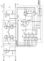
- FIG. 1 is a circuit diagram of a bidirectional DC-DC converter according to an embodiment.
- FIG. 2 is a timing chart for explaining the operation of the switching control unit when the control mode is switched.
- FIG. 3 is a circuit diagram of another example of a bidirectional DC-DC converter.
- FIG. 1 is a circuit diagram of a bidirectional DC-DC converter 1 according to this embodiment.
- the bidirectional DC-DC converter 1 includes a pair of input / output terminals IO11 and IO12, and a pair of input / output terminals IO21 and IO22.
- the input / output terminal IO11 and the input / output terminal IO12 are examples of the “first input / output unit” according to the invention.
- the input / output terminal IO21 and the input / output terminal IO22 are examples of the “second input / output unit” according to the present invention.
- the bidirectional DC-DC converter 1 is driven in one of four control modes.
- the bidirectional DC-DC converter 1 boosts the voltage input from the input / output terminal IO11 and the input / output terminal IO12 and outputs the boosted voltage from the input / output terminal IO21 and the input / output terminal IO22.
- the bidirectional DC-DC converter 1 steps down the voltage input from the input / output terminal IO11 and the input / output terminal IO12 and outputs the voltage from the input / output terminal IO21 and the input / output terminal IO22.
- the bidirectional DC-DC converter 1 boosts the voltage input from the input / output terminal IO21 and the input / output terminal IO22 and outputs the boosted voltage from the input / output terminal IO11 and the input / output terminal IO22.
- the bidirectional DC-DC converter 1 steps down the voltage input from the input / output terminal IO21 and the input / output terminal IO22 and outputs the voltage from the input / output terminal IO11 and the input / output terminal IO22.
- the bidirectional DC-DC converter 1 can bidirectionally convert power between the input / output terminal IO11 and the input / output terminal IO12 and the input / output terminal IO21 and the input / output terminal IO22.
- the bidirectional DC-DC converter 1 Power can be supplied from the secondary battery to the load, and power can be supplied from the power source to the secondary battery to charge the secondary battery.
- the converter unit 10 is connected between the input / output terminals IO11 and IO12 and the input / output terminals IO21 and IO22.
- the converter unit 10 includes a capacitor C1, a series circuit of a switch element Q11 and a switch element Q12, a series circuit of a switch element Q21 and a switch element Q22, a capacitor C2, and an inductor L1.
- the capacitor C1 and the series circuit of the switch element Q11 and the switch element Q12 are connected between the input / output terminal IO11 and the input / output terminal IO12, respectively.
- the switch element Q11 and the switch element Q12 are MOS-FETs.
- Capacitor C2 and a series circuit of switch element Q21 and switch element Q22 are connected between input / output terminal IO21 and input / output terminal IO22, respectively.
- the switch element Q21 and the switch element Q22 are MOS-FETs.
- Inductor L1 is connected between a connection point between switch elements Q11 and Q12 and a connection point between switch elements Q21 and Q22.
- the bidirectional DC-DC converter 1 is a so-called H-bridge circuit having a symmetrical circuit configuration with the inductor L1 as the center. Since the H bridge circuit is non-insulated, an increase in size of the bidirectional DC-DC converter 1 can be suppressed.
- the switching control of the converter unit 10 will be described later.
- the voltage detection circuit 11 is connected between the input / output terminal IO11 and the input / output terminal IO12.
- the voltage detection circuit 11 is a voltage dividing circuit of a resistor R11 and a resistor R12.
- the voltage detection circuit 11 detects the voltage V1 with respect to the input / output terminal IO11 and the input / output terminal IO12.
- the voltage V1 is the input voltage of the bidirectional DC-DC converter 1.
- the voltage V1 is the output voltage of the bidirectional DC-DC converter 1.
- the voltage detection circuit 11 is an example of the “first input / output voltage detection unit” according to the present invention.
- the voltage detection circuit 12 is connected between the input / output terminal IO21 and the input / output terminal IO22.
- the voltage detection circuit 12 is a voltage dividing circuit of a resistor R21 and a resistor R22.
- the voltage detection circuit 12 detects the voltage V2 with respect to the input / output terminal IO21 and the input / output terminal IO22.
- the voltage V2 is the input voltage of the bidirectional DC-DC converter 1.
- the voltage V2 is the output voltage of the bidirectional DC-DC converter 1.
- the voltage detection circuit 12 is an example of the “second input / output voltage detection unit” according to the present invention.
- the bidirectional DC-DC converter 1 includes a control unit 13.
- the control unit 13 includes a SW switching unit 14, an error amplification unit 15, and a switching control unit 16.
- the control unit 13 includes a switch S11, a switch S12, a switch S21, a switch S22, a switch S23, and a switch S24.
- the SW switch 14 receives a switching signal from the outside.
- the switching signal is a signal for switching the control mode of the bidirectional DC-DC converter 1.
- the SW switching unit 14 switches the switches S11, S12, and S21 to S24. Further, the SW switching unit 14 outputs a received switching signal to the switching control unit 16.
- the SW switching unit 14 is an example of the “switching signal receiving unit” according to the present invention.
- Switch S11 and switch S12 are single-pole double-throw switches that output one of two inputs. Output voltages from the voltage detection circuit 11 and the voltage detection circuit 12 are input to the switch S11 and the switch S12, respectively, and one of them is output. When the input / output terminal IO11 and the input / output terminal IO12 are on the input side, the switch S11 and the output voltage of the voltage detection circuit 12 are output from the switch S11, and the output voltage of the voltage detection circuit 11 is output from the switch S12. Switch S12 is switched. That is, according to the control mode of the bidirectional DC-DC converter 1, the output voltage of the bidirectional DC-DC converter 1 is output from the switch S11, and the input voltage of the bidirectional DC-DC converter 1 is output from the switch S12. As described above, the switch S11 and the switch S12 are switched.
- the output of the switch S11 is connected to the error amplifying unit 15 and the terminal Vo of the switching control unit 16, respectively.
- the terminal Vo is a terminal for inputting the output voltage of the bidirectional DC-DC converter 1.
- the output of the switch S12 is connected to the terminal Vi of the switching control unit 16.
- the terminal Vi is a terminal for inputting the input voltage of the bidirectional DC-DC converter 1.
- the switching control unit 16 determines a step-down or step-up control mode based on the input voltage and output voltage of the bidirectional DC-DC converter 1 input to the terminal Vi and the terminal Vo.
- the error amplification unit 15 compares the output voltage of the bidirectional DC-DC converter 1, that is, the output voltage of the voltage detection circuit 11 or the voltage detection circuit 12, with the reference voltage Vref.
- the output of the error amplifying unit 15 is connected to the CP (COMP) terminal of the switching control unit 16.
- the switching control unit 16 determines the switching duty of the converter unit 10 based on the output of the error amplification unit 15 and generates a PWM-modulated gate signal.
- the output voltage of the bidirectional DC-DC converter 1 is input to one error amplifying unit 15. Then, the output voltage of the bidirectional DC-DC converter 1 is compared with the same reference voltage Vref.
- the reference voltage may be changed by an external command or a voltage of a secondary battery connected to input / output.
- the error amplifier 15 includes an error amplifier 151 and a phase compensation circuit 152.
- the phase compensation circuit 152 is configured by connecting a capacitor C3 and a resistor R3 in series. By providing the phase compensation circuit 152, stability and responsiveness can be improved.
- the capacitor C3 is an example of the “integration element” according to the present invention.
- the reference voltage Vref is input to the non-inverting input terminal of the error amplifier 151.
- the output of the switch S11 is connected to the inverting input terminal of the error amplifier 151. That is, the output voltage from the voltage detection circuit 11 or the voltage detection circuit 12 is input to the inverting input terminal of the error amplifier 151.
- the phase compensation circuit 152 is a circuit for performing phase compensation of the negative feedback loop, and is connected between the output terminal and the inverting input terminal of the error amplifier 151.
- the switches S21 to S24 are single-pole double-throw switches having one input terminal and two first output terminals and second output terminals.
- the switches S21 to S24 are respectively connected to the terminal HI, the terminal LI, the terminal HO, and the terminal LO of the switching control unit 16 that outputs a gate signal to each switch element of the converter unit 10.
- the input terminal of the switch S21 is connected to the terminal HI of the switching control unit 16.
- the first output terminal of the switch S21 is connected to the gate of the switch element Q11.
- a second output terminal of the switch S21 is connected to the gate of the switch element Q21.
- the input terminal of the switch S22 is connected to the terminal LI of the switching control unit 16.
- the first output terminal of the switch S22 is connected to the gate of the switch element Q12.
- a second output terminal of the switch S22 is connected to the gate of the switch element Q22.
- the input terminal of the switch S23 is connected to the terminal HO of the switching control unit 16.
- the first output terminal of the switch S23 is connected to the gate of the switch element Q21.
- a second output terminal of the switch S23 is connected to the gate of the switch element Q11.
- the input terminal of the switch S24 is connected to the terminal LO of the switching control unit 16.
- the first output terminal of the switch S24 is connected to the gate of the switch element Q22.
- a second output terminal of the switch S24 is connected to the gate of the switch element Q12.
- the switches S21 to S24 are switched by the SW switching unit 14 in accordance with the control mode of the bidirectional DC-DC converter 1.
- the switch S21, the switch S22, the switch S23, and the switch S24 are switched so that the input terminal and the first output terminal are connected. It is done. That is, the terminal HI is connected to the switch element Q11, the terminal LI is connected to the switch element Q12, the terminal HO is connected to the switch element Q21, and the terminal LO is connected to the switch element Q22.
- the switch S21, the switch S22, the switch S23, and the switch S24 are switched so that the input terminal and the second output terminal are connected. That is, the terminal HI is connected to the switch element Q21, the terminal LI is connected to the switch element Q22, the terminal HO is connected to the switch element Q11, and the terminal LO is connected to the switch element Q12.
- the bidirectional DC-DC converter 1 boosts the input voltage from the input / output terminal IO11 and the input / output terminal IO12 and outputs the boosted voltage from the input / output terminal IO21 and the input / output terminal IO22.
- the SW switching unit 14 switches the switch S11 so that the output voltage of the voltage detection circuit 12 is input to the error amplification unit 15.
- the error amplifying unit 15 compares the output voltage of the voltage detection circuit 12 with the reference voltage Vref and outputs it to the switching control unit 16.
- the switching control unit 16 determines the duty ratio of the switching control from the comparison result.
- the switching control unit 16 always turns on the switch element Q11 and always turns off the switch element Q12. Then, the switching control unit 16 turns on and off the switch elements Q21 and Q22 alternately with the determined duty ratio. At this time, the switch element Q21 operates as a synchronous rectifier element.
- the bidirectional DC-DC converter 1 steps down the input voltage from the input / output terminal IO11 and the input / output terminal IO12 and outputs it from the input / output terminal IO21 and the input / output terminal IO22.
- the SW switching unit 14 switches the switch S11 so that the output voltage of the voltage detection circuit 12 is input to the error amplification unit 15.
- the error amplifying unit 15 compares the output voltage of the voltage detection circuit 12 with the reference voltage Vref and outputs it to the switching control unit 16.
- the switching control unit 16 determines the duty ratio of the switching control from the comparison result.
- the switching control unit 16 always turns on the switch element Q21 and always turns off the switch element Q22. Then, the switching control unit 16 turns on and off the switching elements Q11 and Q12 alternately with the determined duty ratio. At this time, the switch element Q12 operates as a synchronous rectifier element.
- the bidirectional DC-DC converter 1 boosts the input voltage from the input / output terminal IO21 and the input / output terminal IO22 and outputs the boosted voltage from the input / output terminal IO11 and the input / output terminal IO12.
- the SW switching unit 14 switches the switch S11 so that the output voltage of the voltage detection circuit 11 is input to the error amplification unit 15.
- the error amplifying unit 15 compares the output voltage of the voltage detection circuit 11 with the reference voltage Vref and outputs the result to the switching control unit 16.
- the switching control unit 16 determines the duty ratio of the switching control from the comparison result.
- the switching control unit 16 always turns on the switch element Q21 and always turns off the switch element Q22. Then, the switching control unit 16 turns on and off the switching elements Q11 and Q12 alternately with the determined duty ratio. At this time, the switch element Q11 operates as a synchronous rectifier element.
- the bidirectional DC-DC converter 1 steps down the input voltage from the input / output terminal IO21 and the input / output terminal IO22 and outputs it from the input / output terminal IO11 and the input / output terminal IO12.
- the SW switching unit 14 switches the switch S11 so that the output voltage of the voltage detection circuit 11 is input to the error amplification unit 15.
- the error amplifying unit 15 compares the output voltage of the voltage detection circuit 11 with the reference voltage Vref and outputs the result to the switching control unit 16.
- the switching control unit 16 determines the duty ratio of the switching control from the comparison result.
- the switching control unit 16 always turns on the switch element Q11 and always turns off the switch element Q12. Then, the switching control unit 16 turns on and off the switch elements Q21 and Q22 alternately with the determined duty ratio. At this time, the switch element Q22 operates as a synchronous rectifier element.
- the bidirectional DC-DC converter 1 can be driven in any one of the first control mode, the second control mode, the third control mode, and the fourth control mode.
- the switching of the power supply direction is performed according to an external switching signal received by the SW switching unit 14.
- the switching signal is notified to the switching control unit 16.
- the switching control unit 16 switches the power supply direction according to the switching signal.
- the switching control unit 16 stops the switching control for a predetermined period.
- FIG. 2 is a timing chart for explaining the operation of the switching control unit 16 when the control mode is switched. In this example, it is assumed that the bidirectional DC-DC converter 1 is driven in the first control mode until time t1.
- the switching control unit 16 performs switching control until time t1 when the SW switching unit 14 receives a switching signal.
- the switching control unit 16 turns off all the switch elements Q11, Q12, Q21, and Q22 and stops the switching control.
- the SW switching unit 14 switches the switch S11 and the like after the time t2 has elapsed from the time t1.
- the switching control unit 16 starts the switching control so that the bidirectional DC-DC converter 1 is driven in the control mode based on the received switching signal when the time t3 has elapsed. To do.
- the capacitor C3 functions as an integration element, so that charge is used as information for the deviation between the output voltage and the reference value to be zero. Is stored. If the direction of power supply is switched in this state, the control becomes unstable due to the accumulated charge, and an abnormal operation such as excessive or insufficient duty may occur. Further, although it is necessary to switch from the step-up operation to the step-down operation, if there is a capacitor on the Vi and Vo lines of the control unit 13 as a parasitic component or intentionally for noise removal, the capacitor is switched after the switching is performed. There is also a possibility that the boosting operation may be continuously performed during a transition period in which the voltage changes.
- the switching control is stopped for a predetermined period Td.
- the predetermined period Td is a period until the switching control is ready to control by switching the direction of power supply.
- the SW switching unit 14 switches the switch S11 and the like after the elapse of time t5 from time t4.
- FIG. 3 is a circuit diagram of another example bidirectional DC-DC converter 1A.
- the error amplifying unit 15A includes a phase compensation circuit 152A.
- the phase compensation circuit 152A has a series circuit of a capacitor C3 and a resistor R3, and the capacitors C4 and C5 constitute a differential element. Capacitors C4 and C5 are connected in parallel to resistors R11 and R21 of voltage detection circuits 11 and 12, respectively. A series circuit of the capacitor C3 and the resistor R3 is connected between the output terminal and the inverting input terminal of the error amplifier 151. By providing the capacitors C4 and C5, the feedback phase can be advanced, so that the response can be improved.
- the bidirectional DC-DC converter 1 has been described as an H-bridge circuit.
- the bidirectional DC-DC converter 1 can be appropriately changed as long as the circuit can perform bidirectional power conversion between two input / output units.
Landscapes
- Engineering & Computer Science (AREA)
- Power Engineering (AREA)
- Dc-Dc Converters (AREA)
Abstract
双方向DC-DCコンバータ(1)は、入出力端子(IO11,IO12)と入出力端子(IO21,IO22)との間で双方向に電力変換するコンバータ部(10)と、電力変換方向を切り替える切替信号を受信するSW切替部(14)と、入出力電圧を検出する電圧検出回路(11)及び電圧検出回路(12)と、SW切替部(14)が受信する切替信号と、電圧検出回路(11)又は電圧検出回路(12)による検出結果とに基づいて、コンバータ部(10)をスイッチング制御するスイッチング制御部(16)とを備える。スイッチング制御部(16)は、切替信号を受信したとき、スイッチング制御を停止し、期間経過後にスイッチング制御を開始する。
Description
本発明は、2つの入出力部の間で双方向に電力変換を行う双方向DC-DCコンバータに関する。
特許文献1には、絶縁型の双方向DC-DCコンバータが開示されている。この双方向DC-DCコンバータは、入力側の接続と出力側の接続を変更することなく、電圧検出回路及び駆動回路を電力供給の方向に応じて切り替えることで、DC-DCコンバータの入力側から出力側への電力供給及び出力側から入力側への電力供給を可能としている。
しかしながら、特許文献1の双方向DC-DCコンバータにおいて、電力供給の方向が切り替わる直後は、制御が不安定になり、また、異常動作を引き起こすおそれがある。例えば、出力電圧が入力電圧より高い場合は双方向DC-DCコンバータが、入力側から出力側へ昇圧動作を行うことになるが、このとき電力供給方向を切り替えると、出力側から入力側へは降圧動作を行うべきであるにもかかわらず、切り替えた直後は昇圧動作を維持し、過大に電力を供給するおそれがある。
そこで、本発明の目的は、安定した動作を行う双方向DC-DCコンバータを提供することにある。
本発明に係る双方向DC-DCコンバータは、第1入出力部及び第2入出力部と、前記第1入出力部と前記第2入出力部との間で双方向に電力変換するコンバータ部と、電力変換方向を切り替える切替信号を受信する切替信号受信部と、前記第1入出力部に対する入出力電圧を検出する第1入出力電圧検出部と、前記第2入出力部に対する入出力電圧を検出する第2入出力電圧検出部と、前記切替信号受信部が受信する切替信号と、前記第1入出力電圧検出部又は前記第2入出力電圧検出部による検出結果とに基づいて、前記コンバータ部をスイッチング制御するスイッチング制御部と、を備え、前記スイッチング制御部は、前記切替信号受信部が切替信号を受信したとき、スイッチング制御を停止し、所定期間経過後にスイッチング制御を開始する、ことを特徴とする。
この構成では、切替信号を受信したとき、所定期間、例えばスイッチング制御部に含まれる容量に蓄電された電荷が放電されるまでの間、スイッチング制御を停止することで、制御を安定させて電力変換方向を切り替えることができる。
前記双方向DC-DCコンバータは、前記第1入出力電圧検出部又は前記第2入出力電圧検出部による検出結果と、基準値とを比較する誤差増幅部を備え、前記誤差増幅部は積分要素を含む位相補償回路を有し、前記スイッチング制御部は、前記誤差増幅部の出力に基づいてスイッチング制御してもよい。
この構成では、位相補償回路を設けることで、安定性と応答性の改善を図れる。また、位相補償回路に含まれる積分要素により、出力電圧と基準値の偏差をゼロに近づけることができる。
前記位相補償回路は微分要素を含んでもよい。
この構成では、位相補償回路に含まれる微分要素により、応答速度を高めることができる。
前記コンバータ部は、Hブリッジコンバータであってもよい。
この構成では、非絶縁とすることで、双方向DC-DCコンバータの大型化を抑制できる。
本発明によれば、所定期間、例えばスイッチング制御部に含まれる容量に蓄電された電荷が放電されるまでの間、スイッチング制御を停止することで、電力変換方向を切り替えた後の制御を安定させることができる。
図1は、本実施形態に係る双方向DC-DCコンバータ1の回路図である。
双方向DC-DCコンバータ1は、一対の入出力端子IO11と入出力端子IO12と、一対の入出力端子IO21と入出力端子IO22とを備える。入出力端子IO11及び入出力端子IO12は、本発明に係る「第1入出力部」の一例である。入出力端子IO21及び入出力端子IO22は、本発明に係る「第2入出力部」の一例である。
本実施形態に係る双方向DC-DCコンバータ1は、4つの制御モードの何れかで駆動する。第1制御モードでは、双方向DC-DCコンバータ1は、入出力端子IO11及び入出力端子IO12から入力される電圧を昇圧して、入出力端子IO21及び入出力端子IO22から出力する。第2制御モードでは、双方向DC-DCコンバータ1は、入出力端子IO11及び入出力端子IO12から入力される電圧を降圧して、入出力端子IO21及び入出力端子IO22から出力する。第3制御モードでは、双方向DC-DCコンバータ1は、入出力端子IO21及び入出力端子IO22から入力される電圧を昇圧して、入出力端子IO11及び入出力端子IO22から出力する。第4制御モードでは、双方向DC-DCコンバータ1は、入出力端子IO21及び入出力端子IO22から入力される電圧を降圧して、入出力端子IO11及び入出力端子IO22から出力する。
つまり、双方向DC-DCコンバータ1は、入出力端子IO11及び入出力端子IO12と、入出力端子IO21及び入出力端子IO22との間で、双方向に電力変換が可能である。例えば、入出力端子IO11及び入出力端子IO12には電源又は負荷が接続され、入出力端子IO21及び入出力端子IO22には二次電池が接続される場合、双方向DC-DCコンバータ1は、二次電池から負荷へ電力を供給し、また、電源から二次電池へ電力を供給して、二次電池を充電することができる。
入出力端子IO11及び入出力端子IO12と、入出力端子IO21及び入出力端子IO22との間には、コンバータ部10が接続される。コンバータ部10は、キャパシタC1と、スイッチ素子Q11及びスイッチ素子Q12の直列回路と、スイッチ素子Q21及びスイッチ素子Q22の直列回路と、キャパシタC2と、インダクタL1とで構成される。
キャパシタC1と、スイッチ素子Q11及びスイッチ素子Q12の直列回路はそれぞれ、入出力端子IO11と入出力端子IO12との間に接続される。スイッチ素子Q11とスイッチ素子Q12はMOS-FETである。キャパシタC2と、スイッチ素子Q21及びスイッチ素子Q22の直列回路はそれぞれ、入出力端子IO21と入出力端子IO22との間に接続される。スイッチ素子Q21とスイッチ素子Q22はMOS-FETである。インダクタL1は、スイッチ素子Q11とスイッチ素子Q12との接続点と、スイッチ素子Q21とスイッチ素子Q22との接続点との間に接続される。
つまり、双方向DC-DCコンバータ1は、インダクタL1を中心とした対称型の回路構成を有する、所謂Hブリッジ回路である。Hブリッジ回路は非絶縁であるため、双方向DC-DCコンバータ1の大型化を抑制できる。コンバータ部10のスイッチング制御については後述する。
入出力端子IO11と入出力端子IO12との間には電圧検出回路11が接続される。電圧検出回路11は、抵抗R11と抵抗R12との分圧回路である。電圧検出回路11は、入出力端子IO11及び入出力端子IO12に対する電圧V1を検出する。入出力端子IO11及び入出力端子IO12が入力側となる場合には、電圧V1は双方向DC-DCコンバータ1の入力電圧である。入出力端子IO11及び入出力端子IO12が出力側となる場合には、電圧V1は双方向DC-DCコンバータ1の出力電圧である。電圧検出回路11は、本発明に係る「第1入出力電圧検出部」の一例である。
入出力端子IO21と入出力端子IO22との間には電圧検出回路12が接続される。電圧検出回路12は、抵抗R21と抵抗R22との分圧回路である。電圧検出回路12は、入出力端子IO21及び入出力端子IO22に対する電圧V2を検出する。入出力端子IO21及び入出力端子IO22が入力側となる場合には、電圧V2は双方向DC-DCコンバータ1の入力電圧である。入出力端子IO21及び入出力端子IO22が出力側となる場合には、電圧V2は双方向DC-DCコンバータ1の出力電圧である。電圧検出回路12は、本発明に係る「第2入出力電圧検出部」の一例である。
双方向DC-DCコンバータ1は制御部13を備える。制御部13は、SW切替部14と、誤差増幅部15と、スイッチング制御部16とを有する。また、制御部13は、スイッチS11と、スイッチS12と、スイッチS21と、スイッチS22と、スイッチS23と、スイッチS24とを有する。
SW切替部14は外部から切替信号を受信する。切替信号は、双方向DC-DCコンバータ1の制御モードを切り替える信号である。SW切替部14は、切替信号を受信するとスイッチS11,S12,S21~S24を切り替える。また、SW切替部14は、受信する切替信号をスイッチング制御部16へ出力する。SW切替部14は、本発明に係る「切替信号受信部」の一例である。
スイッチS11及びスイッチS12は、2つの入力の一方を出力する単極双投形のスイッチである。スイッチS11及びスイッチS12それぞれには、電圧検出回路11及び電圧検出回路12それぞれからの出力電圧が入力され、それらの一方を出力する。入出力端子IO11及び入出力端子IO12が入力側となる場合、電圧検出回路12の出力電圧がスイッチS11から出力され、電圧検出回路11の出力電圧がスイッチS12から出力されるように、スイッチS11及びスイッチS12は切り替えられる。つまり、双方向DC-DCコンバータ1の制御モードに応じて、スイッチS11からは双方向DC-DCコンバータ1の出力電圧が出力され、スイッチS12からは双方向DC-DCコンバータ1の入力電圧が出力されるように、スイッチS11及びスイッチS12は切り替えられる。
スイッチS11の出力は、誤差増幅部15と、スイッチング制御部16の端子Voそれぞれに接続される。端子Voは、双方向DC-DCコンバータ1の出力電圧を入力するための端子である。スイッチS12の出力は、スイッチング制御部16の端子Viに接続される。端子Viは、双方向DC-DCコンバータ1の入力電圧を入力するための端子である。スイッチング制御部16は、端子Viと端子Voに入力された、双方向DC-DCコンバータ1の入力電圧と出力電圧とに基づき、降圧または昇圧の制御モードを決定する。
誤差増幅部15は、双方向DC-DCコンバータ1の出力電圧、すなわち電圧検出回路11又は電圧検出回路12の出力電圧と、基準電圧Vrefとを比較する。誤差増幅部15の出力は、スイッチング制御部16のCP(COMP)端子に接続される。スイッチング制御部16は、誤差増幅部15の出力に基づいて、コンバータ部10のスイッチングデューティを決定し、PWM変調したゲート信号を生成する。
双方向DC-DCコンバータ1の制御モードにかかわらず、双方向DC-DCコンバータ1の出力電圧は、1つの誤差増幅部15に入力される。そして、双方向DC-DCコンバータ1の出力電圧は、同じ基準電圧Vrefと比較される。なお、この基準電圧は外部の指令又は入出力に接続する二次電池の電圧などによって変更されてもよい。
誤差増幅部15は、誤差増幅器151と、位相補償回路152とを有する。位相補償回路152はキャパシタC3と抵抗R3とが直列接続されて構成される。位相補償回路152を設けることで、安定性と応答性との改善を図ることができる。キャパシタC3は、本発明に係る「積分要素」の一例である。誤差増幅器151の非反転入力端子には、基準電圧Vrefが入力される。誤差増幅器151の反転入力端子には、スイッチS11の出力が接続される。つまり、誤差増幅器151の反転入力端子には、電圧検出回路11又は電圧検出回路12からの出力電圧が入力される。位相補償回路152は、負帰還ループの位相補償を行うための回路であり、誤差増幅器151の出力端子と反転入力端子との間に接続される。
スイッチS21~S24は、一つの入力端子と、二つの第1出力端子及び第2出力端子とを有する単極双投形のスイッチである。スイッチS21~S24は、コンバータ部10の各スイッチ素子へゲート信号を出力する、スイッチング制御部16の端子HIと、端子LIと、端子HOと、端子LOとにそれぞれ接続される。
スイッチS21の入力端子は、スイッチング制御部16の端子HIに接続される。スイッチS21の第1出力端子は、スイッチ素子Q11のゲートに接続される。スイッチS21の第2出力端子は、スイッチ素子Q21のゲートに接続される。
スイッチS22の入力端子は、スイッチング制御部16の端子LIに接続される。スイッチS22の第1出力端子は、スイッチ素子Q12のゲートに接続される。スイッチS22の第2出力端子は、スイッチ素子Q22のゲートに接続される。
スイッチS23の入力端子は、スイッチング制御部16の端子HOに接続される。スイッチS23の第1出力端子は、スイッチ素子Q21のゲートに接続される。スイッチS23の第2出力端子は、スイッチ素子Q11のゲートに接続される。
スイッチS24の入力端子は、スイッチング制御部16の端子LOに接続される。スイッチS24の第1出力端子は、スイッチ素子Q22のゲートに接続される。スイッチS24の第2出力端子は、スイッチ素子Q12のゲートに接続される。
スイッチS21~S24は、双方向DC-DCコンバータ1の制御モードに応じてSW切替部14により切り替えられる。第1制御モード又は第2制御モードでは、図1に示すように、スイッチS21と、スイッチS22と、スイッチS23と、スイッチS24とは、入力端子と第1出力端子とが接続されるように切り替えられる。つまり、端子HIはスイッチ素子Q11に接続され、端子LIはスイッチ素子Q12に接続され、端子HOはスイッチ素子Q21に接続され、端子LOはスイッチ素子Q22に接続される。第3制御モード又は第4制御モードでは、スイッチS21と、スイッチS22と、スイッチS23と、スイッチS24とは、入力端子と第2出力端子とが接続されるように切り替えられる。つまり、端子HIはスイッチ素子Q21に接続され、端子LIはスイッチ素子Q22に接続され、端子HOはスイッチ素子Q11に接続され、端子LOはスイッチ素子Q12に接続される。
次に、前記のように構成される双方向DC-DCコンバータ1の動作について説明する。
(第1制御モード)
第1制御モードでは、双方向DC-DCコンバータ1は、入出力端子IO11及び入出力端子IO12からの入力電圧を昇圧して、入出力端子IO21及び入出力端子IO22から出力する。この場合、SW切替部14は、電圧検出回路12の出力電圧が誤差増幅部15に入力されるようにスイッチS11を切り替える。誤差増幅部15は、電圧検出回路12の出力電圧と基準電圧Vrefとを比較し、スイッチング制御部16へ出力する。スイッチング制御部16は、その比較結果から、スイッチング制御のデューティ比を決定する。
第1制御モードでは、双方向DC-DCコンバータ1は、入出力端子IO11及び入出力端子IO12からの入力電圧を昇圧して、入出力端子IO21及び入出力端子IO22から出力する。この場合、SW切替部14は、電圧検出回路12の出力電圧が誤差増幅部15に入力されるようにスイッチS11を切り替える。誤差増幅部15は、電圧検出回路12の出力電圧と基準電圧Vrefとを比較し、スイッチング制御部16へ出力する。スイッチング制御部16は、その比較結果から、スイッチング制御のデューティ比を決定する。
スイッチング制御部16は、スイッチ素子Q11を常時オン、スイッチ素子Q12を常時オフする。そして、スイッチング制御部16は、決定したデューティ比でスイッチ素子Q21とスイッチ素子Q22とを交互にオンオフする。このとき、スイッチ素子Q21は同期整流素子として動作する。
(第2制御モード)
第2制御モードでは、双方向DC-DCコンバータ1は、入出力端子IO11及び入出力端子IO12からの入力電圧を降圧して、入出力端子IO21及び入出力端子IO22から出力する。この場合、SW切替部14は、電圧検出回路12の出力電圧が誤差増幅部15に入力されるようにスイッチS11を切り替える。誤差増幅部15は、電圧検出回路12の出力電圧と基準電圧Vrefとを比較し、スイッチング制御部16へ出力する。スイッチング制御部16は、その比較結果から、スイッチング制御のデューティ比を決定する。
第2制御モードでは、双方向DC-DCコンバータ1は、入出力端子IO11及び入出力端子IO12からの入力電圧を降圧して、入出力端子IO21及び入出力端子IO22から出力する。この場合、SW切替部14は、電圧検出回路12の出力電圧が誤差増幅部15に入力されるようにスイッチS11を切り替える。誤差増幅部15は、電圧検出回路12の出力電圧と基準電圧Vrefとを比較し、スイッチング制御部16へ出力する。スイッチング制御部16は、その比較結果から、スイッチング制御のデューティ比を決定する。
スイッチング制御部16は、スイッチ素子Q21を常時オン、スイッチ素子Q22を常時オフする。そして、スイッチング制御部16は、決定したデューティ比でスイッチ素子Q11とスイッチ素子Q12とを交互にオンオフする。このとき、スイッチ素子Q12は同期整流素子として動作する。
(第3制御モード)
第3制御モードでは、双方向DC-DCコンバータ1は、入出力端子IO21及び入出力端子IO22からの入力電圧を昇圧して、入出力端子IO11及び入出力端子IO12から出力する。この場合、SW切替部14は、電圧検出回路11の出力電圧が誤差増幅部15に入力されるようにスイッチS11を切り替える。誤差増幅部15は、電圧検出回路11の出力電圧と基準電圧Vrefとを比較し、スイッチング制御部16へ出力する。スイッチング制御部16は、その比較結果から、スイッチング制御のデューティ比を決定する。
第3制御モードでは、双方向DC-DCコンバータ1は、入出力端子IO21及び入出力端子IO22からの入力電圧を昇圧して、入出力端子IO11及び入出力端子IO12から出力する。この場合、SW切替部14は、電圧検出回路11の出力電圧が誤差増幅部15に入力されるようにスイッチS11を切り替える。誤差増幅部15は、電圧検出回路11の出力電圧と基準電圧Vrefとを比較し、スイッチング制御部16へ出力する。スイッチング制御部16は、その比較結果から、スイッチング制御のデューティ比を決定する。
スイッチング制御部16は、スイッチ素子Q21を常時オン、スイッチ素子Q22を常時オフする。そして、スイッチング制御部16は、決定したデューティ比でスイッチ素子Q11とスイッチ素子Q12とを交互にオンオフする。このとき、スイッチ素子Q11は同期整流素子として動作する。
(第4制御モード)
第4制御モードでは、双方向DC-DCコンバータ1は、入出力端子IO21及び入出力端子IO22からの入力電圧を降圧して、入出力端子IO11及び入出力端子IO12から出力する。この場合、SW切替部14は、電圧検出回路11の出力電圧が誤差増幅部15に入力されるようにスイッチS11を切り替える。誤差増幅部15は、電圧検出回路11の出力電圧と基準電圧Vrefとを比較し、スイッチング制御部16へ出力する。スイッチング制御部16は、その比較結果から、スイッチング制御のデューティ比を決定する。
第4制御モードでは、双方向DC-DCコンバータ1は、入出力端子IO21及び入出力端子IO22からの入力電圧を降圧して、入出力端子IO11及び入出力端子IO12から出力する。この場合、SW切替部14は、電圧検出回路11の出力電圧が誤差増幅部15に入力されるようにスイッチS11を切り替える。誤差増幅部15は、電圧検出回路11の出力電圧と基準電圧Vrefとを比較し、スイッチング制御部16へ出力する。スイッチング制御部16は、その比較結果から、スイッチング制御のデューティ比を決定する。
スイッチング制御部16は、スイッチ素子Q11を常時オン、スイッチ素子Q12を常時オフする。そして、スイッチング制御部16は、決定したデューティ比でスイッチ素子Q21とスイッチ素子Q22とを交互にオンオフする。このとき、スイッチ素子Q22は同期整流素子として動作する。
このように、双方向DC-DCコンバータ1は、第1制御モード、第2制御モード、第3制御モード、及び第4制御モードの何れかで駆動できる。そして、電力供給方向の切り替えは、SW切替部14が受信する外部からの切替信号に従って行われる。SW切替部14が切替信号を受信すると、この切替信号がスイッチング制御部16へ通知される。スイッチング制御部16は、切替信号に応じて、電力供給方向を切り替える。スイッチング制御部16は、電力供給方向を切り替える際、所定期間、スイッチング制御を停止する。
図2は、制御モードの切り替え時のスイッチング制御部16の動作を説明するためのタイミングチャートである。この例では、時刻t1まで、双方向DC-DCコンバータ1は第1制御モードで駆動しているものとする。
SW切替部14が切替信号を受信する時刻t1までは、スイッチング制御部16は、スイッチング制御を行っている。時刻t1にSW切替部14が切替信号を受信すると、スイッチング制御部16は、スイッチ素子Q11,Q12,Q21,Q22のすべてをオフにして、スイッチング制御を停止する。SW切替部14は、時刻t1から時刻t2の経過後、スイッチS11等を切り替える。スイッチング制御部16は、時刻t1でスイッチング制御を停止した後、時刻t3を経過したときに、受信した切替信号に基づく制御モードで双方向DC-DCコンバータ1が駆動するように、スイッチング制御を開始する。
例えば、双方向DC-DCコンバータ1が第1制御モードで駆動している場合、キャパシタC3は積分要素として機能しているため、出力電圧と基準値との偏差がゼロとなるための情報として電荷が蓄えられている。この状態で電力供給の方向を切り替えると、蓄えられた電荷に起因して、制御が不安定となり、また、デューティが過大又は過少になるなどの異常動作するおそれがある。また、昇圧動作から降圧動作へ切り替える必要があるが、制御部13のVi及びVoの線路に、寄生成分として、又はノイズ除去のため意図的にキャパシタが存在する場合、切り替えが行われてからキャパシタの電圧が変化する過渡期間に昇圧動作が引き続き行われるおそれもある。
そこで、図2で説明したように、制御モードを切り替える際、所定期間Td、スイッチング制御を停止する。この所定期間Tdは、スイッチング制御が電力供給の方向を切り替えて制御する準備ができるまでの期間である。これにより、電力供給方向の切り替え後も、双方向DC-DCコンバータ1は、安定した制御を行うことができる。
なお、時刻t4で切替信号を受信して、再び電力供給方向を切り替える場合も同様に、SW切替部14は、時刻t4から時刻t5の経過後、スイッチS11等を切り替える。
図3は、別の例の双方向DC-DCコンバータ1Aの回路図である。この例では、誤差増幅部15Aの構成が図1と相違する。誤差増幅部15Aは、位相補償回路152Aを有する。位相補償回路152Aは、キャパシタC3と抵抗R3との直列回路を有し、キャパシタC4,C5とが微分要素を構成する。キャパシタC4,C5は、それぞれの電圧検出回路11,12の抵抗R11,R21に並列に接続される。キャパシタC3と抵抗R3との直列回路は、誤差増幅器151の出力端子と反転入力端子との間に接続される。キャパシタC4,C5を設けることで、フィードバック位相を進ませることができるので、応答性の改善を図れる。
電力供給の方向を切り替えた場合、キャパシタC4及びキャパシタC5の接続が急に変更されるため、微分要素の働きにより誤差増幅器151の出力が急激に変化して異常動作するおそれがある。しかし、図2で説明したように、制御モードを切り替える際、所定期間Td、スイッチング制御を停止させることにより、誤差増幅器151の出力が急激に変化したとしてもスイッチング制御が停止しているため、安定して電力供給の方向を切り替えることができる。
なお、上述の実施形態では、双方向DC-DCコンバータ1はHブリッジ回路として説明したが、2つの入出力部の間で双方向に電力変換を行える回路であれば適宜変更可能である。
C1,C2,C3,C4,C5…キャパシタ
IO11,IO12…入出力端子(第1入出力部)
IO21,IO22…入出力端子(第2入出力部)
L1…インダクタ
Q11,Q12,Q21,Q22…スイッチ素子
R11,R12…抵抗
R21,R22…抵抗
R3…抵抗
S11,S12,S21,S22,S23,S24…スイッチ
1,1A…DC-DCコンバータ
10…コンバータ部
11…電圧検出回路(第1入出力電圧検出部)
12…電圧検出回路(第2入出力電圧検出部)
13…制御部
14…SW切替部(切替信号受信部)
15,15A…誤差増幅部
16…スイッチング制御部
151…誤差増幅器
152,152A…位相補償回路
IO11,IO12…入出力端子(第1入出力部)
IO21,IO22…入出力端子(第2入出力部)
L1…インダクタ
Q11,Q12,Q21,Q22…スイッチ素子
R11,R12…抵抗
R21,R22…抵抗
R3…抵抗
S11,S12,S21,S22,S23,S24…スイッチ
1,1A…DC-DCコンバータ
10…コンバータ部
11…電圧検出回路(第1入出力電圧検出部)
12…電圧検出回路(第2入出力電圧検出部)
13…制御部
14…SW切替部(切替信号受信部)
15,15A…誤差増幅部
16…スイッチング制御部
151…誤差増幅器
152,152A…位相補償回路
Claims (4)
- 第1入出力部及び第2入出力部と、
前記第1入出力部と前記第2入出力部との間で双方向に電力変換するコンバータ部と、
電力変換方向を切り替える切替信号を受信する切替信号受信部と、
前記第1入出力部に対する入出力電圧を検出する第1入出力電圧検出部と、
前記第2入出力部に対する入出力電圧を検出する第2入出力電圧検出部と、
前記切替信号受信部が受信する切替信号と、前記第1入出力電圧検出部又は前記第2入出力電圧検出部による検出結果とに基づいて、前記コンバータ部をスイッチング制御するスイッチング制御部と、
を備え、
前記スイッチング制御部は、
前記切替信号受信部が切替信号を受信したとき、スイッチング制御を停止し、所定期間経過後にスイッチング制御を開始する、
双方向DC-DCコンバータ。 - 前記第1入出力電圧検出部又は前記第2入出力電圧検出部による検出結果と、基準値とを比較する誤差増幅部、
を備え、
前記誤差増幅部は積分要素を含む位相補償回路を有し、
前記スイッチング制御部は、前記誤差増幅部の出力に基づいてスイッチング制御する、
請求項1に記載の双方向DC-DCコンバータ。 - 前記位相補償回路は微分要素を含む、
請求項2に記載の双方向DC-DCコンバータ。 - 前記コンバータ部はHブリッジコンバータである、
請求項1から3の何れかに記載の双方向DC-DCコンバータ。
Applications Claiming Priority (2)
| Application Number | Priority Date | Filing Date | Title |
|---|---|---|---|
| JP2016096694 | 2016-05-13 | ||
| JP2016-096694 | 2016-05-13 |
Publications (1)
| Publication Number | Publication Date |
|---|---|
| WO2017195591A1 true WO2017195591A1 (ja) | 2017-11-16 |
Family
ID=60266975
Family Applications (1)
| Application Number | Title | Priority Date | Filing Date |
|---|---|---|---|
| PCT/JP2017/016473 Ceased WO2017195591A1 (ja) | 2016-05-13 | 2017-04-26 | 双方向dc-dcコンバータ |
Country Status (1)
| Country | Link |
|---|---|
| WO (1) | WO2017195591A1 (ja) |
Cited By (1)
| Publication number | Priority date | Publication date | Assignee | Title |
|---|---|---|---|---|
| CN107979168A (zh) * | 2017-12-22 | 2018-05-01 | 厦门科华恒盛股份有限公司 | 一种数据中心不间断供电系统 |
Citations (7)
| Publication number | Priority date | Publication date | Assignee | Title |
|---|---|---|---|---|
| JPH06269162A (ja) * | 1993-03-11 | 1994-09-22 | Hitachi Lighting Ltd | 電源装置 |
| JP2003052170A (ja) * | 2001-08-03 | 2003-02-21 | Texas Instr Japan Ltd | Dc−dcコンバータ |
| JP2004343855A (ja) * | 2003-05-14 | 2004-12-02 | Taiyo Yuden Co Ltd | 電源装置 |
| WO2007125949A1 (ja) * | 2006-04-27 | 2007-11-08 | Panasonic Corporation | 双方向dc-dcコンバータ |
| JP2007325478A (ja) * | 2006-06-05 | 2007-12-13 | Torex Device Co Ltd | スイッチング電源回路 |
| JP2014093910A (ja) * | 2012-11-06 | 2014-05-19 | Nippon Steel & Sumikin Texeng Co Ltd | 二次電池用双方向電源装置及びその制御方法 |
| JP2015162951A (ja) * | 2014-02-27 | 2015-09-07 | 株式会社 日立産業制御ソリューションズ | 双方向コンバータ |
-
2017
- 2017-04-26 WO PCT/JP2017/016473 patent/WO2017195591A1/ja not_active Ceased
Patent Citations (7)
| Publication number | Priority date | Publication date | Assignee | Title |
|---|---|---|---|---|
| JPH06269162A (ja) * | 1993-03-11 | 1994-09-22 | Hitachi Lighting Ltd | 電源装置 |
| JP2003052170A (ja) * | 2001-08-03 | 2003-02-21 | Texas Instr Japan Ltd | Dc−dcコンバータ |
| JP2004343855A (ja) * | 2003-05-14 | 2004-12-02 | Taiyo Yuden Co Ltd | 電源装置 |
| WO2007125949A1 (ja) * | 2006-04-27 | 2007-11-08 | Panasonic Corporation | 双方向dc-dcコンバータ |
| JP2007325478A (ja) * | 2006-06-05 | 2007-12-13 | Torex Device Co Ltd | スイッチング電源回路 |
| JP2014093910A (ja) * | 2012-11-06 | 2014-05-19 | Nippon Steel & Sumikin Texeng Co Ltd | 二次電池用双方向電源装置及びその制御方法 |
| JP2015162951A (ja) * | 2014-02-27 | 2015-09-07 | 株式会社 日立産業制御ソリューションズ | 双方向コンバータ |
Cited By (1)
| Publication number | Priority date | Publication date | Assignee | Title |
|---|---|---|---|---|
| CN107979168A (zh) * | 2017-12-22 | 2018-05-01 | 厦门科华恒盛股份有限公司 | 一种数据中心不间断供电系统 |
Similar Documents
| Publication | Publication Date | Title |
|---|---|---|
| US9154031B2 (en) | Current mode DC-DC conversion device with fast transient response | |
| US9595869B2 (en) | Multi-level switching regulator circuits and methods with finite state machine control | |
| TWI528694B (zh) | 切換模式電源控制器及用於控制切換模式電源之方法 | |
| US20210067042A1 (en) | Multi-phase switched capacitor power converter and control method thereof | |
| CN103929049B (zh) | 恒定导通时间控制电路及直流转直流转换电路 | |
| US9401642B2 (en) | Switching power-supply device | |
| US9716434B2 (en) | Switch control circuit and control method for a four-switch buck-boost converter | |
| JP2018523446A (ja) | スイッチングレギュレータ及びその制御方法 | |
| US11664734B2 (en) | Flyback converter for controlling on time variation | |
| KR102267648B1 (ko) | Dc/dc 컨버터 | |
| JP5951358B2 (ja) | 充電制御回路および充電回路 | |
| KR20100086995A (ko) | 전원 장치 | |
| JP4998094B2 (ja) | Dc−dcコンバータ | |
| US9270177B1 (en) | Switching power-supply device | |
| US9455632B1 (en) | Voltage converter | |
| CN103532378A (zh) | 抑制输出电压过冲的电压转换器 | |
| JP4341698B2 (ja) | スイッチング電源とその制御回路及び制御方法 | |
| JP6205596B2 (ja) | ソフトスタート回路及び電源装置 | |
| US10135332B2 (en) | DC-DC converter | |
| JP4887841B2 (ja) | Dc−dcコンバータ制御回路、dc−dcコンバータ、半導体装置およびdc−dcコンバータ制御方法 | |
| KR101404568B1 (ko) | 전류 모드 제어의 펄스폭변조 변환 장치 | |
| JP2018098973A (ja) | 昇降圧dc/dcコンバータ | |
| JP5966503B2 (ja) | 昇降圧型dc−dcコンバータおよび携帯機器 | |
| WO2017195591A1 (ja) | 双方向dc-dcコンバータ | |
| JP2019106832A (ja) | モータ駆動装置 |
Legal Events
| Date | Code | Title | Description |
|---|---|---|---|
| NENP | Non-entry into the national phase |
Ref country code: DE |
|
| 121 | Ep: the epo has been informed by wipo that ep was designated in this application |
Ref document number: 17795952 Country of ref document: EP Kind code of ref document: A1 |
|
| 122 | Ep: pct application non-entry in european phase |
Ref document number: 17795952 Country of ref document: EP Kind code of ref document: A1 |
|
| NENP | Non-entry into the national phase |
Ref country code: JP |