WO2017195560A1 - 表示装置および電子機器 - Google Patents
表示装置および電子機器 Download PDFInfo
- Publication number
- WO2017195560A1 WO2017195560A1 PCT/JP2017/015896 JP2017015896W WO2017195560A1 WO 2017195560 A1 WO2017195560 A1 WO 2017195560A1 JP 2017015896 W JP2017015896 W JP 2017015896W WO 2017195560 A1 WO2017195560 A1 WO 2017195560A1
- Authority
- WO
- WIPO (PCT)
- Prior art keywords
- electrode
- sub
- electrodes
- display device
- pixel
- Prior art date
- Legal status (The legal status is an assumption and is not a legal conclusion. Google has not performed a legal analysis and makes no representation as to the accuracy of the status listed.)
- Ceased
Links
Images






Classifications
-
- H—ELECTRICITY
- H10—SEMICONDUCTOR DEVICES; ELECTRIC SOLID-STATE DEVICES NOT OTHERWISE PROVIDED FOR
- H10K—ORGANIC ELECTRIC SOLID-STATE DEVICES
- H10K59/00—Integrated devices, or assemblies of multiple devices, comprising at least one organic light-emitting element covered by group H10K50/00
- H10K59/10—OLED displays
- H10K59/12—Active-matrix OLED [AMOLED] displays
- H10K59/122—Pixel-defining structures or layers, e.g. banks
-
- H—ELECTRICITY
- H10—SEMICONDUCTOR DEVICES; ELECTRIC SOLID-STATE DEVICES NOT OTHERWISE PROVIDED FOR
- H10K—ORGANIC ELECTRIC SOLID-STATE DEVICES
- H10K50/00—Organic light-emitting devices
- H10K50/80—Constructional details
- H10K50/805—Electrodes
- H10K50/81—Anodes
- H10K50/813—Anodes characterised by their shape
-
- H—ELECTRICITY
- H10—SEMICONDUCTOR DEVICES; ELECTRIC SOLID-STATE DEVICES NOT OTHERWISE PROVIDED FOR
- H10K—ORGANIC ELECTRIC SOLID-STATE DEVICES
- H10K50/00—Organic light-emitting devices
- H10K50/80—Constructional details
- H10K50/805—Electrodes
- H10K50/82—Cathodes
- H10K50/822—Cathodes characterised by their shape
-
- H—ELECTRICITY
- H10—SEMICONDUCTOR DEVICES; ELECTRIC SOLID-STATE DEVICES NOT OTHERWISE PROVIDED FOR
- H10K—ORGANIC ELECTRIC SOLID-STATE DEVICES
- H10K50/00—Organic light-emitting devices
- H10K50/80—Constructional details
- H10K50/84—Passivation; Containers; Encapsulations
- H10K50/844—Encapsulations
-
- H—ELECTRICITY
- H10—SEMICONDUCTOR DEVICES; ELECTRIC SOLID-STATE DEVICES NOT OTHERWISE PROVIDED FOR
- H10K—ORGANIC ELECTRIC SOLID-STATE DEVICES
- H10K59/00—Integrated devices, or assemblies of multiple devices, comprising at least one organic light-emitting element covered by group H10K50/00
- H10K59/80—Constructional details
- H10K59/805—Electrodes
- H10K59/8051—Anodes
- H10K59/80515—Anodes characterised by their shape
-
- H—ELECTRICITY
- H10—SEMICONDUCTOR DEVICES; ELECTRIC SOLID-STATE DEVICES NOT OTHERWISE PROVIDED FOR
- H10K—ORGANIC ELECTRIC SOLID-STATE DEVICES
- H10K59/00—Integrated devices, or assemblies of multiple devices, comprising at least one organic light-emitting element covered by group H10K50/00
- H10K59/80—Constructional details
- H10K59/805—Electrodes
- H10K59/8051—Anodes
- H10K59/80518—Reflective anodes, e.g. ITO combined with thick metallic layers
-
- H—ELECTRICITY
- H10—SEMICONDUCTOR DEVICES; ELECTRIC SOLID-STATE DEVICES NOT OTHERWISE PROVIDED FOR
- H10K—ORGANIC ELECTRIC SOLID-STATE DEVICES
- H10K71/00—Manufacture or treatment specially adapted for the organic devices covered by this subclass
-
- H—ELECTRICITY
- H10—SEMICONDUCTOR DEVICES; ELECTRIC SOLID-STATE DEVICES NOT OTHERWISE PROVIDED FOR
- H10K—ORGANIC ELECTRIC SOLID-STATE DEVICES
- H10K2102/00—Constructional details relating to the organic devices covered by this subclass
- H10K2102/301—Details of OLEDs
- H10K2102/341—Short-circuit prevention
-
- H—ELECTRICITY
- H10—SEMICONDUCTOR DEVICES; ELECTRIC SOLID-STATE DEVICES NOT OTHERWISE PROVIDED FOR
- H10K—ORGANIC ELECTRIC SOLID-STATE DEVICES
- H10K50/00—Organic light-emitting devices
- H10K50/80—Constructional details
- H10K50/805—Electrodes
- H10K50/81—Anodes
- H10K50/818—Reflective anodes, e.g. ITO combined with thick metallic layers
-
- H—ELECTRICITY
- H10—SEMICONDUCTOR DEVICES; ELECTRIC SOLID-STATE DEVICES NOT OTHERWISE PROVIDED FOR
- H10K—ORGANIC ELECTRIC SOLID-STATE DEVICES
- H10K50/00—Organic light-emitting devices
- H10K50/80—Constructional details
- H10K50/85—Arrangements for extracting light from the devices
- H10K50/856—Arrangements for extracting light from the devices comprising reflective means
-
- H—ELECTRICITY
- H10—SEMICONDUCTOR DEVICES; ELECTRIC SOLID-STATE DEVICES NOT OTHERWISE PROVIDED FOR
- H10K—ORGANIC ELECTRIC SOLID-STATE DEVICES
- H10K59/00—Integrated devices, or assemblies of multiple devices, comprising at least one organic light-emitting element covered by group H10K50/00
- H10K59/80—Constructional details
- H10K59/87—Passivation; Containers; Encapsulations
- H10K59/873—Encapsulations
-
- H—ELECTRICITY
- H10—SEMICONDUCTOR DEVICES; ELECTRIC SOLID-STATE DEVICES NOT OTHERWISE PROVIDED FOR
- H10K—ORGANIC ELECTRIC SOLID-STATE DEVICES
- H10K59/00—Integrated devices, or assemblies of multiple devices, comprising at least one organic light-emitting element covered by group H10K50/00
- H10K59/80—Constructional details
- H10K59/875—Arrangements for extracting light from the devices
- H10K59/878—Arrangements for extracting light from the devices comprising reflective means
-
- H—ELECTRICITY
- H10—SEMICONDUCTOR DEVICES; ELECTRIC SOLID-STATE DEVICES NOT OTHERWISE PROVIDED FOR
- H10K—ORGANIC ELECTRIC SOLID-STATE DEVICES
- H10K71/00—Manufacture or treatment specially adapted for the organic devices covered by this subclass
- H10K71/861—Repairing
Definitions
- the present disclosure relates to a display device using an organic EL (electroluminescence) element and an electronic apparatus including the display device.
- an anode and a cathode may be electrically short-circuited to cause a pixel defect called a dark spot.
- a technique for repairing (repairing) such a short-circuited portion has been proposed (for example, Patent Document 1).
- a display device includes a plurality of pixels, and each of the plurality of pixels is formed on the first electrode including the plurality of sub-electrodes and the plurality of sub-electrodes.
- An insulating film having an opening facing each other, an organic layer formed in each opening of the insulating film and including a light emitting layer, and a second electrode formed on the organic layer.
- An electronic apparatus includes the display device according to the embodiment of the present disclosure.
- the first electrode includes a plurality of sub-electrodes, so that in the selective pixel, the first electrode and the second electrode are electrically connected to each other due to foreign matters. Even when short-circuited, a part of the sub-electrode corresponding to the short-circuited portion can be selectively cut.
- an image is displayed by the display device according to the embodiment of the present disclosure.
- the first electrode in each pixel, includes a plurality of sub-electrodes, and the insulating film has an opening facing each sub-electrode.
- An organic layer is formed in the opening.
- FIG. 1 is a block diagram illustrating an overall configuration of a display device according to an embodiment of the present disclosure.
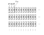
- FIG. 2 is a schematic diagram illustrating an arrangement of pixels illustrated in FIG. 1.
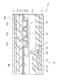
- FIG. 2 is a cross-sectional view illustrating a partial configuration of a pixel portion illustrated in FIG. 1.
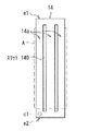
- FIG. 4 is a plan view illustrating a configuration example of a first electrode illustrated in FIG. 3.
- FIG. 4 is a plan view illustrating a configuration of a first insulating film illustrated in FIG. 3 together with a configuration of a first electrode.
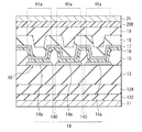
- FIG. 6 is a cross-sectional view illustrating a configuration corresponding to the line IB-IB in FIG. 5. It is sectional drawing showing the detailed structure of the opening part (reflector) shown in FIG.
- FIG. 10 is a schematic diagram for explaining defect repair according to Comparative Example 1.
- FIG. 10 is a schematic diagram for explaining defect repair according to Comparative Example 2.
- FIG. It is a schematic diagram for demonstrating the effect by the defect repair shown in FIG.
- FIG. It is a schematic diagram for demonstrating the effect by the opening part shown in FIG. 3 and
- FIG. 10 is a plan view illustrating a configuration of a first electrode according to Modification 1-1.
- FIG. 12 is a plan view illustrating a configuration of a first electrode according to Modification 1-2.
- FIG. 10 is a plan view illustrating a configuration of a first electrode according to Modification 1-3.
- FIG. 14 is a plan view illustrating a configuration of a first electrode according to Modification 2-1.
- FIG. 14 is a plan view illustrating a configuration of a first electrode according to Modification 2-2.
- FIG. 12 is a plan view illustrating a configuration of a first electrode according to Modification 3-1.
- FIG. 12 is a plan view illustrating a configuration of a first electrode according to Modification 3-2.
- FIG. 10 is a plan view illustrating a configuration of a first electrode according to Modification 4.
- FIG. 10 is a cross-sectional view illustrating a configuration of a pixel unit according to Modification Example 5. It is a block diagram showing the function structure of the example of application.
- Embodiment Example of display device in which first electrode is divided into a plurality of sub-electrodes and an opening having a reflector is provided for each sub-electrode
- Modifications 1-1 to 1-3 (Other examples of sub electrode stripe arrangement) 3.
- Modified examples 2-1 and 2-2 (examples where the surface shape of the sub-electrode is circular or elliptical) 4).
- Modified examples 3-1 and 3-2 other examples of sub-electrode dividing directions) 5.
- Modification 4 (Another example of the surface shape of the first electrode) 6).
- Modification 5 (Other configuration example of the pixel portion) 7).
- Application examples (examples of electronic devices)
- FIG. 1 illustrates an overall configuration of a display device (display device 1) according to an embodiment of the present disclosure.
- the display device 1 is, for example, an organic EL display using an organic electroluminescence element, and for example, light of any color of R (red), G (green), and B (blue) is emitted from the upper surface side.
- the display device 1 includes, for example, a pixel unit 2 and a circuit unit (scanning line driving unit 3, signal line driving unit 4, and power supply line driving unit 5) for driving the pixel unit 2.
- the pixel unit 2 has a plurality of pixels pr, pg, and pb that are two-dimensionally arranged.
- the pixel unit 2 displays an image based on a video signal input from the outside by, for example, an active matrix method.
- the pixel unit 2 includes a plurality of scanning lines WSL extending along the row direction of the pixel array, a plurality of signal lines DTL extending along the column direction, and a plurality of signal lines DTL extending along the row direction.
- a power supply line DSL is provided.
- These scanning lines WSL, signal lines DTL, and power supply lines DSL are electrically connected to the pixels pr, pg, pb.
- Each of the pixels pr, pg, and pb corresponds to, for example, a subpixel, and a set of these pixels pr, pg, and pb constitutes one pixel (pixel Pix).
- FIG. 2 shows an example of a planar configuration of the pixel Pix (pixels pr, pg, pb) shown in FIG.
- Each surface shape of the pixels pr, pg, pb has a rectangular shape, for example, and is arranged in a stripe shape as a whole.
- pixels having the same emission color are arranged side by side.
- the pixel pr is for displaying red (R)
- the pixel pg is for displaying green (G), for example
- the pixel pb is for displaying blue (B), for example.
- Each of these pixels pr, pg, and pb has a pixel circuit PXLC including the organic EL element 10.
- pixels P when it is not necessary to distinguish each of the pixels pr, pg, and pb, they will be referred to as “pixels P”.
- the pixel circuit PXLC controls light emission and extinction in each pixel pr, pg, pb, and includes, for example, an organic EL element 10, a storage capacitor Cs, a write transistor WsTr, and a drive transistor DsTr. Yes.
- the circuit configuration of 2Tr1C is illustrated as the pixel circuit PXLC, but the configuration of the pixel circuit PXLC is not limited to this.
- the pixel circuit PXLC may have a circuit configuration in which various capacitors, transistors, and the like are further added to the 2Tr1C circuit.
- the write transistor WsTr controls application of a video signal (signal voltage) to the gate electrode of the drive transistor DsTr. Specifically, the write transistor WsTr samples the voltage (signal voltage) of the signal line DTL according to the voltage applied to the scanning line WSL, and writes the signal voltage to the gate electrode of the drive transistor DsTr.
- the drive transistor DsTr is connected in series to the organic EL element 10 and controls the current flowing through the organic EL element 10 according to the magnitude of the signal voltage sampled by the write transistor WsTr.
- the drive transistor DsTr and the write transistor WsTr are formed by, for example, an n-channel MOS type or a p-channel MOS type thin film transistor (TFT: Thin Film Transistor). These drive transistor DsTr and write transistor WsTr may be a single gate type or a dual gate type.
- the holding capacitor Cs holds a predetermined voltage between the gate electrode and the source electrode of the driving transistor DsTr.
- the gate electrode of the writing transistor WsTr is connected to the scanning line WSL.
- One of the source electrode and the drain electrode of the write transistor WsTr is connected to the signal line DTL, and the other electrode is connected to the gate electrode of the drive transistor DsTr.
- One of the source electrode and the drain electrode of the drive transistor DsTr is connected to the power supply line DSL, and the other electrode is connected to an anode (first electrode 14 described later) of the organic EL element 10.
- the storage capacitor Cs is inserted between the gate electrode of the drive transistor DsTr and the electrode on the organic EL element 10 side.
- the scanning line WSL is for supplying each pixel P with a selection pulse for selecting a plurality of pixels P arranged in the pixel unit 2 for each row.
- the scanning line WSL is connected to an output end (not shown) of the scanning line driving unit 3 and a gate electrode of a writing transistor WsTr described later.
- the signal line DTL is for supplying a signal pulse (signal potential Vsig and reference potential Vofs) corresponding to the video signal to each pixel P.
- the signal line DTL is connected to an output end (not shown) of the signal line driver 4 and a source electrode or a drain electrode of a write transistor WsTr described later.
- the power supply line DSL is for supplying a fixed potential (Vcc) to each pixel P as electric power.
- the power supply line DSL is connected to an output end (not shown) of the power supply line driving unit 5 and a source electrode or a drain electrode of a drive transistor DsTr described later.
- the cathode (second electrode 17 described later) of the organic EL element 10 is connected to a common potential line (cathode line).
- the scanning line driving unit 3 outputs a predetermined selection pulse to each scanning line WSL in a line-sequential manner, thereby performing operations such as anode reset, Vth correction, signal potential Vsig writing, mobility correction, and light emission operation, for example.
- Each pixel P is executed at a predetermined timing.
- the signal line drive unit 4 generates an analog video signal corresponding to a digital video signal input from the outside, and outputs the analog video signal to each signal line DTL.
- the power line driver 5 outputs a constant potential to each power line DSL.
- the scanning line driving unit 3, the signal line driving unit 4, and the power supply line driving unit 5 are controlled so as to operate in conjunction with each other by a timing control signal output from a timing control unit (not shown).
- a digital video signal input from the outside is corrected by a video signal receiving unit (not shown) and then input to the signal line driving unit 4.
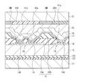
- FIG. 3 shows a partial cross-sectional configuration of the display device 1 (pixel unit 2).
- a plurality of organic EL elements 10 are two-dimensionally arranged on the drive substrate 11a.
- a region corresponding to one organic EL element 10 (corresponding to a pixel pr that displays red). (Region) only.
- the second substrate 21 is interposed via a second insulating film 18, a sealing layer 19, a color filter layer (red filter 20R, green filter 20G, blue filter 20B) and a black matrix layer BM. Are pasted together.
- the drive substrate 11a is obtained by forming a pixel circuit including the TFT 12 (the pixel circuit PXLC shown in FIG. 1) on the first substrate 11 made of, for example, glass or plastic.
- the surface of the drive substrate 11a is flattened by the flattening film 13.
- the TFT 12 corresponds to, for example, the drive transistor DsTr shown in FIG.
- the TFT 12 has, for example, a gate electrode 121 in a selective region on the first substrate 11, and a semiconductor layer 123 on the gate electrode 121 through a gate insulating film 122.
- An interlayer insulating film 124 is formed on the semiconductor layer 123.
- a pair of source / drain electrodes 125 is provided on the interlayer insulating film 124. These source / drain electrodes 125 are electrically connected to the semiconductor layer 123 through contact holes provided in the interlayer insulating film 124.
- One of the pair of source / drain electrodes 125 is electrically connected to the first electrode 14 through a contact portion c1 (anode contact).
- the TFT 12 has a so-called bottom gate structure as an example.
- the present invention is not limited to this, and the TFT 12 may have a so-called top gate structure.
- the gate electrode 121 includes at least one of metals such as molybdenum (Mo), titanium (Ti), aluminum (Al), tungsten (W), and chromium (Cr).
- the gate insulating film 122 and the interlayer insulating film 124 include, for example, at least one of silicon oxide (SiO 2 ), silicon nitride (SiNx), silicon oxynitride (SiON), and the like.
- the semiconductor layer 123 is formed of a silicon-based semiconductor such as amorphous silicon (amorphous silicon), polycrystalline silicon (polysilicon), and microcrystalline silicon, or an oxide such as indium gallium zinc oxide (InGaZnO) and zinc oxide (ZnO). It is composed of a physical semiconductor.
- the source / drain electrode 125 is configured to include at least one of metals such as molybdenum, titanium, aluminum, tungsten, and chromium.
- the planarizing film 13 is made of, for example, an organic insulating material such as polyimide or acrylic resin.
- the organic EL element 10 On the driving substrate 11a, the organic EL element 10 is formed for each of the pixels pr, pg, and pb. As shown in FIG. 3, the organic EL element 10 has an organic layer 16 and a second electrode 17 on the first electrode 14. A plurality of first electrodes 14 are arranged on the drive substrate 11a, and a first insulating film 15 (insulating film) is formed so as to cover the plurality of first electrodes 14. The first insulating film 15 has a plurality of openings (openings H1a) facing each first electrode 14. The organic layer 16 is formed in each opening H1a of the first insulating film 15.
- the first electrode 14 is, for example, a reflective electrode that functions as an anode, and is provided for each pixel P.
- the constituent material of the first electrode 14 include metal elements such as aluminum (Al), chromium, gold (Au), platinum (Pt), nickel (Ni), copper (Cu), tungsten, or silver (Ag).
- metal elements such as aluminum (Al), chromium, gold (Au), platinum (Pt), nickel (Ni), copper (Cu), tungsten, or silver (Ag).
- a simple substance or an alloy is mentioned.
- the first electrode 14 may include a laminated film of a metal film made of a single element or an alloy of these metal elements and a light-transmitting conductive material (transparent conductive film).
- the transparent conductive film include ITO (indium tin oxide), IZO (indium zinc oxide), and zinc oxide (ZnO) based materials.
- zinc oxide-based material include zinc oxide (AZO) to which aluminum (Al) is added and zinc oxide
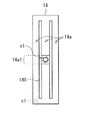
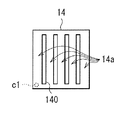
- FIG. 4 shows a planar configuration of the first electrode 14.
- the first electrode 14 is divided (subdivided) and includes a plurality of sub-electrodes (sub-electrode portions) 14a.
- three sub-electrodes 14a are arranged in a region A of the first electrode 14 that contributes to light emission.
- Each sub-electrode 14a is disposed to face the opening H1a of the first insulating film 15.
- These three sub-electrodes 14a are connected (electrically connected) at the end portions (end portions e1 and e2) of the first electrode 14.
- the first electrode 14 has a plurality of (here, two) slits 140, and each slit 140 extends along the long side direction of the rectangular shape of the first electrode 14.
- the first electrode 14 (specifically, a part of the first electrode 14) is divided into a plurality of sub-electrodes 14a.
- the dividing direction in the region A is along the rectangular long side direction of the first electrode 14.
- a part of the first electrode 14 (a region 14a1 corresponding to a short-circuited portion on a sub electrode 14a described later) is selectively cut.
- the surface shape of the first electrode 14 (the shape of the surface parallel to the substrate surface) is, for example, a rectangular shape.
- the surface shape of the sub-electrode 14a is not particularly limited.
- the sub-electrode 14a has a rectangular shape having long sides along the long-side direction of the rectangular shape of the first electrode 14.
- a plurality of sub-electrodes 14a are arranged in a stripe shape, for example.
- each sub-electrode 14a has a rectangular shape extending along one direction (arranged extending straight along one direction), but each sub-electrode 14a is meanderingly arranged. Alternatively, they may be arranged in a zigzag shape. Further, it may be bent or curved in part.
- the width, size, shape, and the like of the sub-electrodes 14a may be the same or different.
- the first insulating film 15 is for defining the light emitting region of each pixel P and ensuring the insulation between the first electrode 14 and the second electrode 17.
- the first insulating film 15 also functions as a so-called partition wall when the organic layer 16 is formed using a wet process.
- the first insulating film 15 is, for example, a photosensitive resin such as an acrylic resin, a polyimide resin, a fluorine resin, a silicon resin, a fluorine polymer, a silicon polymer, a novolac resin, an epoxy resin, or a norbornene resin. It is comprised including. Or what disperse
- the first insulating film 15 may be made of an inorganic material such as silicon oxide, silicon nitride, or silicon oxynitride.
- FIG. 5 shows the planar configuration of the first insulating film 15 together with the planar configuration of the first electrode 14.
- FIG. 6 shows a cross-sectional configuration taken along line IB-IB in FIG.
- the configuration shown in FIG. 3 corresponds to the cross-sectional configuration taken along the line IA-IA in FIG.
- the first insulating film 15 has a plurality (three in this case) of openings H1a facing one first electrode 14.
- Each opening H1a is disposed to face the sub electrode 14a (a region of the first insulating film 15 facing the sub electrode 14a is opened).
- On the bottom surface of each opening H1a for example, the sub electrode 14a, the organic layer 16, and the second electrode 17 are stacked in this order.
- one organic EL element 10 has three effective light emitting regions defined by the three openings H1a.
- the opening H1a of the first insulating film 15 desirably has a reflector (reflection structure) 40 as described below, for example. This is because the light extraction efficiency can be improved and the luminance can be increased (decrease in luminance due to dark spots can be suppressed).
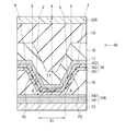
- FIG. 7 shows a detailed configuration in the vicinity of the opening H1a.
- the reflector 40 has a function of guiding the light generated from the organic layer 16 toward the front by reflection using a reflection interface formed in the vicinity of the inclined surface PS of the first insulating film 15.
- the reflector 40 includes, for example, the constituent material (refractive index) of the first insulating film 15, the shape and the inclination angle ⁇ of the inclined surface PS of the opening H1a, and the constituent materials (second insulating film 18 and the sealing layer 19). (Refractive index) and the combination.
- the first electrode 14 (sub-electrode 14 a) has a laminated structure of an Al alloy layer 141 and an ITO layer 142. As the organic layer 16, hole injection is sequentially performed from the first electrode 14 side. The case where the transport layer 161, the light emitting layer 162, and the electron transport layer 163 are formed is shown.
- the refractive index of the first insulating film 15 is preferably different from the refractive index of the second insulating film 18. This is because a reflective interface is formed by the difference in refractive index between the first insulating film 15 and the second insulating film 18. It is desirable that the refractive index n2 of the second insulating film 18 and the refractive index n1 of the first insulating film 15 satisfy the following expressions (1) and (2). Thereby, light can be efficiently reflected at the reflection interface between the first insulating film 15 and the second insulating film 18.
- the thickness (height) t of the first insulating film 15, the opening length R1 on the lower end side of the opening H1a, and the opening length R2 on the upper end side of the opening H1a are expressed by the following equations (3) and ( It is desirable to satisfy 4). Thereby, light can be efficiently reflected at the reflection interface between the first insulating film 15 and the second insulating film 18.
- the organic layer 16 includes, for example, an organic electroluminescent layer (light emitting layer) that generates white light, and is formed as a common layer for a plurality of pixels pr, pg, pb in the pixel unit 2, for example.
- the organic layer 16 may include, for example, a hole injection layer, a hole transport layer, and an electron transport layer as necessary.
- the light emitting layer included in the organic layer 16 has a configuration in which, for example, a red light emitting layer, a green light emitting layer, and a blue light emitting layer are stacked. Or you may have the structure which laminated
- the light emitting layer may be formed as a light emitting layer having a different color for each of the pixels pr, pg, and pb.
- the organic layer 16 formed in the pixel pr includes a red light emitting layer
- the organic layer 16 formed in the pixel pg includes a green light emitting layer
- the organic layer 16 formed in the pixel pb includes a blue light emitting layer. Formed with.
- the second electrode 17 functions as, for example, a cathode, and is formed over the entire surface of the pixel portion 2 (as an electrode common to all the pixels P).
- the second electrode 17 is made of, for example, a transparent conductive film.
- the transparent conductive film include ITO (indium tin oxide), IZO (indium zinc oxide), and zinc oxide (ZnO) based materials.
- the zinc oxide-based material include zinc oxide (AZO) to which aluminum (Al) is added and zinc oxide (GZO) to which gallium (Ga) is added.
- the thickness of the second electrode 17 is not particularly limited, but may be set in consideration of conductivity and light transmittance. In addition to this, an alloy of magnesium and silver (MgAg alloy) may be used for the second electrode 17.
- the second insulating film 18 is provided so as to cover the second electrode 17 and is made of, for example, silicon nitride.
- the second insulating film 18 is provided to increase the reflection efficiency of the reflector 40, and as a protective film for preventing moisture from entering the organic EL element 10 and preventing changes in characteristics such as light emission efficiency. It also has the function of
- the sealing layer 19 seals the organic EL element 10 while bonding the second insulating film 18 and the second substrate 21 together.
- the material of the sealing layer 19 include acrylic resins, polyimide resins, fluorine resins, silicon resins, fluorine polymers, silicon polymers, novolac resins, epoxy resins, and norbornene resins. . Or what disperse
- the color filter layers extract white light generated in each organic EL element 10 as red (R), green (G), and blue (B) color lights. And provided on one surface of the second substrate 21 (for example, the surface on the sealing layer 19 side).
- a red filter 20R is formed in a region facing the organic EL element 10 of the pixel pr
- a green filter 20G is formed in a region facing the organic EL element 10 of the pixel pg
- a blue filter 20B is formed in a region facing the organic EL element 10 of the pixel pb.
- These red filter 20R, green filter 20G, and blue filter 20B are each composed of a resin mixed with a pigment.
- the black matrix layer BM is formed in a region (region between pixels) between the red filter 20R, the green filter 20G, and the blue filter 20B.
- the black matrix layer BM is constituted by, for example, a resin film mixed with a black colorant, or a thin film filter using thin film interference.
- the thin film filter is formed by, for example, laminating one or more thin films made of metal, metal nitride, or metal oxide, and attenuating light by utilizing interference of the thin film.
- Specific examples of the thin film filter include a filter in which Cr and chromium oxide (III) (Cr 2 O 3 ) are alternately laminated.
- the second substrate 21 seals the organic EL element 10 together with the sealing layer 19.
- the second substrate 21 is made of, for example, a material such as glass or plastic that is transparent to the light generated in the organic EL element 10.
- the first electrode 14 includes a plurality of sub-electrodes 14a.
- a description will be given of defect repair when an electrical short circuit (short circuit x1) occurs due to a foreign object.
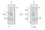
- a part of the first electrode 14 including a part where the short circuit x1 occurs (a part where foreign matter is mixed) (partial region 14a1 of the sub-electrode 14a). Is selectively disconnected.
- the laser used for the repair is not particularly limited, and examples thereof include a laser capable of processing the metal constituting the first electrode 14 or the transparent conductive film, for example, a solid-state laser such as a fiber laser or a YAG laser.
- Comparative Examples 1 and 2 of the present embodiment defect repair when the first electrode (first electrode 101) is not divided will be described.
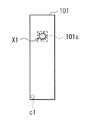
- the location (part 101a) where the short circuit x1 occurs is selectively cut by laser irradiation.
- the laser beam is scanned along the portion 101a including the short circuit x1 (so as to surround the portion where the short circuit x1 occurs), and the repair is not easy.
- an insulating film 102 having, for example, two openings 102a is provided on the same first electrode 101 as in Comparative Example 1 (the left diagram in FIG. 9B). .
- a laser beam is irradiated to an organic layer (not shown) formed in the opening 102a having the short circuit x1.
- the opening 102a (opening 102a1) having the short circuit x1 out of the two openings 102a is darkened (set as a non-light emitting region), and the other opening is formed.
- 102a (opening 102a2) can emit light normally.
- Comparative Example 2 in the pixel in which the short circuit x1 occurs, the light emitting region is narrowed (about half), leading to a decrease in luminance.
- the pixel P is selected by supplying a selection pulse from the scanning line driving unit 3 to the writing transistor WsTr of each pixel P.
- a signal voltage corresponding to the video signal is supplied from the signal line driver 4 to the selected pixel P and is held in the holding capacitor Cs.
- the drive transistor DsTr is on / off controlled in accordance with the signal held in the holding capacitor Cs, and a drive current is injected into the organic EL element 10.
- the organic EL element 10 organic electroluminescent layer
- this light is transmitted through the second electrode 17, the second insulating film 18, the sealing layer 19, the color filter layers (red filter 20R, green filter 20B, blue filter 20B) and the second substrate 21 and extracted.
- red filter 20R, green filter 20B, blue filter 20B red filter layers
- red filter 20R, green filter 20B, blue filter 20B red filter layers
- green light, and blue light are emitted from each pixel P (pixels pr, pg, pb), and color video display is performed by additive color mixing of these color lights.
- the first electrode 14 constituting the organic EL element 10 of each pixel pr, pg, pb includes a plurality of sub-electrodes 14a.
- FIG. 11 is a schematic diagram for explaining the effect of the opening H1a (reflector 40).
- the light emitted from the light emitting layer 162 of the organic layer 16 by the light emission driving as described above includes the forward light L2 in a direction (oblique direction) shifted from the front direction in addition to the light L1 traveling in the front direction.
- the light L2 is reflected and rises in the front direction.
- a part of the sub-electrode 14a corresponding to the short-circuited portion (region 14a1 in FIG. 10) is darkened, but this region 14a1 is smaller than the entire region of the first electrode 14. And since it is a narrow area
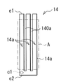
- FIG. 12A shows the configuration of the first electrode 14 according to Modification 1-1.
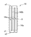
- FIG. 12B shows the configuration of the first electrode 14 according to Modification 1-2.
- FIG. 12C shows the configuration of the first electrode 14 according to Modification 1-3.
- the configuration in which the three sub electrodes 14a are arranged in a stripe shape in the first electrode 14 and the sub electrodes 14a are connected at the end portions (end portions e1 and e2) is illustrated.
- the configuration of the end of the sub-electrode 14a in the first electrode 14 is not limited to this, and can take various forms. The configuration described here is just an example.
- the three sub-electrodes 14a may be connected only at one end (here, the end portion e2).
- the first electrode 14 has a plurality (two in this case) of notches 140a. These notches 140a are open on one side of the end portions e1 and e2 (here, the end portion e1), and extend along the long side direction of the sub-electrode 14a.
- the three sub-electrodes 14a may be alternately folded (bent) at the end portions e1 and e2.
- the first electrode 14 has a plurality of (here, two) notches 140b.
- One of these notches 140b is open on the end e1 side and extends along the long side direction of the sub-electrode 14a, and the other notch 140b is opened on the end e2 side. It extends along the long side direction of 14a.
- any of these modifications 1-1 and 1-2 since the three sub-electrodes 14a are electrically connected, a voltage is applied to each sub-electrode 14a via one contact portion c1. It can be supplied.
- the sub-electrodes 14a in the first electrode 14 may be electrically separated.
- the first electrode 14 has a plurality of (here, two) gaps (gap 140c), and is thus divided into a plurality of sub-electrodes 14a.
- the contact part c1 is arrange
- the first electrode 14 only needs to include a plurality of sub-electrodes 14a in the region A that contributes to light emission, for example, and the configuration of the end portions e1 and e2 (regions other than the region A) is not particularly limited. Further, the number of divisions of the first electrode 14 in the region A (the number of sub-electrodes 14a) is not limited to three as described above, and may be two, or four or more. It doesn't matter.
- FIG. 13A shows the configuration of the first electrode 14 according to Modification 2-1.
- FIG. 13B shows the configuration of the first electrode 14 according to Modification 3-2.
- the surface shape of the sub-electrode 14a has a rectangular shape is illustrated, but the surface shape of the sub-electrode 14a is not limited to the rectangular shape, and may take various shapes.
- the configuration described here is just an example.
- each of the three sub-electrodes (sub-electrodes 14b) in the first electrode 14 may include a circular portion 14b1.
- a plurality of circular portions 14b1 are connected (electrically connected) and arranged.
- each of the three sub-electrodes 14b in the first electrode 14 may include an elliptical portion 14b2.
- a plurality of ellipsoidal portions 14b2 are connected (electrically connected) and arranged.
- the sub-electrodes 14b are electrically connected to each other in a region other than the region A of the first electrode 14, and a voltage is supplied to each sub-electrode 14b through one contact portion c1.
- the first insulating film 15 is provided with the opening H1a having the reflector 40 for each circular portion 14b1 (or for each elliptical portion 14b2). Is desirable.
- the sub-electrode 14b is not limited to the circular shape and the elliptical shape as described above, and may include a polygonal shape (n-corner shape: n is an integer of 3 or 5 or more).
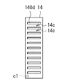
- FIG. 14A shows the configuration of the first electrode 14 according to Modification 3-1.
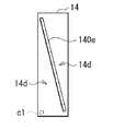
- FIG. 14B shows the configuration of the first electrode 14 according to Modification 3-2.
- the dividing direction of the first electrode 14 is not limited to this.
- the first electrode 14 may be divided along the short side direction of the rectangle.
- the first electrode 14 is provided with a plurality of slits 140d extending along the short side direction, and a plurality of sub-electrodes 14c extending in the short side direction are formed by these slits 140d.
- the first electrode 14 may be divided along the rectangular diagonal direction (oblique direction).
- the first electrode 14 is provided with a slit 140e extending along an oblique direction, and the two sub-electrodes 14d are formed by the slit 140e.
- FIG. 15 illustrates a configuration of the first electrode 14 according to the fourth modification.
- the surface shape of the 1st electrode 14 illustrated the structure which has a rectangular shape
- the surface shape of the 1st electrode 14 is not limited to a rectangular shape.
- the square first electrode 14 may be used.
- the same effect as in the above embodiment can be obtained by arranging a plurality (here, five) of sub-electrodes 14a through the slit 140, as in the above embodiment.
- FIG. 16 illustrates a configuration of a pixel portion according to the fifth modification.
- the configuration in which the organic layer 16 of the organic EL element 10 generates white light for example, a configuration assuming a dry process such as a vacuum deposition method
- the configuration of the pixel portion (organic layer) is this. It is not limited to.
- the organic layers (organic layers 16R, 16G, and 16B) of each color may be formed by, for example, a wet process (printing and coating).
- the pixel isolation film 15 has a stacked structure of a first insulating film 15A and a second insulating film 15B, and functions as a partition wall.
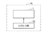
- FIG. 17 shows a functional block configuration of an electronic device (electronic device 1A) to which the display device 1 is applied.
- the electronic device 1A include a television device, a personal computer (PC), a smartphone, a tablet PC, a mobile phone, a digital still camera, a digital video camera, and the like.
- the electronic apparatus 1A includes, for example, the display device 1 and the interface unit 30 described above.
- the interface unit 30 is an input unit to which various signals, a power source, and the like are input from the outside.
- the interface unit 30 may also include a user interface such as a touch panel, a keyboard, or operation buttons.
- the present disclosure has been described with reference to the embodiment, the present disclosure is not limited to the above-described embodiment, and various modifications can be made.
- the reflector 40 of the opening H1a uses the difference in refractive index between the first insulating film 15 and the second insulating film 18, but the side surface of the opening H1a ( A reflective structure can be formed by providing a metal film or the like on the inclined surface PS).
- each layer described in the above embodiments and the like, or the film formation method and film formation conditions are not limited, and may be other materials and thicknesses, or other film formation methods and Film forming conditions may be used.
- the configuration of the organic EL element 10 is specifically described. However, it is not necessary to provide all the layers, and other layers may be further provided.
- the present disclosure can also be applied to a passive matrix display device.
- the configuration of the pixel circuit PXLC for active matrix driving is not limited to that described in the above embodiment, and a capacitor or a transistor may be added as necessary.
- a necessary driving circuit may be added in addition to the scanning line driving unit 3, the signal line driving unit 4, and the power line driving unit 5 described above in accordance with the change of the pixel circuit PXLC.
- Each of the plurality of pixels is A first electrode including a plurality of sub-electrodes; An insulating film formed on the first electrode and having an opening facing each of the plurality of sub-electrodes; An organic layer formed in each opening of the insulating film and including a light emitting layer; And a second electrode formed on the organic layer.
- each surface shape of the plurality of sub-electrodes has a rectangular shape.
- the plurality of sub-electrodes have a stripe shape as a whole.
- each of the plurality of sub-electrodes has a plurality of circular portions or polygonal portions.
- Each of the plurality of pixels is A first electrode including a plurality of sub-electrodes; An insulating film formed on the first electrode and having an opening facing each of the plurality of sub-electrodes; An organic layer formed in each opening of the insulating film and including a light emitting layer; An electronic apparatus comprising: a display device comprising: a second electrode formed on the organic layer.
Landscapes
- Physics & Mathematics (AREA)
- Optics & Photonics (AREA)
- Engineering & Computer Science (AREA)
- Microelectronics & Electronic Packaging (AREA)
- Manufacturing & Machinery (AREA)
- Electroluminescent Light Sources (AREA)
Abstract
この表示装置は、複数の画素を備え、複数の画素はそれぞれ、第1電極と、第1電極上に形成されると共に複数の開口部を有する絶縁膜と、絶縁膜の各開口部に形成されると共に発光層を含む有機層と、有機層上に形成された第2電極とを含み、第1電極は、それぞれが絶縁膜の各開口部に対向して配置された複数のサブ電極を有する。
Description
本開示は、有機EL(electroluminescence)素子を用いた表示装置およびこの表示装置を備えた電子機器に関する。
有機EL表示装置では、例えば製造プロセスにおいて有機層に異物が混入すると、アノードとカソードとが電気的に短絡し、滅点と呼ばれる画素欠陥が生じることがある。このような短絡箇所を修復(リペア)する技術が提案されている(例えば、特許文献1)。
しかしながら、上記特許文献1の手法では、滅点の生じた画素において発光領域が半減し、輝度が低下する。
滅点に起因する輝度低下を抑制して画質を向上させることが可能な表示装置を提供することが望ましい。
本開示の一実施の形態の表示装置は、複数の画素を備え、複数の画素はそれぞれ、複数のサブ電極を含む第1電極と、第1電極上に形成されると共に、複数のサブ電極のそれぞれに対向して開口部を有する絶縁膜と、絶縁膜の各開口部に形成されると共に発光層を含む有機層と、有機層上に形成された第2電極とを有するものである。
本開示の一実施の形態の電子機器は、上記本開示の一実施の形態の表示装置を備えたものである。
本開示の一実施の形態の表示装置および電子機器では、第1電極が複数のサブ電極を含むことにより、選択的な画素において、異物に起因して第1電極および第2電極間が電気的に短絡した場合にも、その短絡箇所に対応するサブ電極の一部を選択的に切断することができる。
本開示の一実施の形態の電子機器では、上記本開示の一実施の形態の表示装置により画像表示がなされる。
本開示の一実施の形態の表示装置および電子機器によれば、各画素において、第1電極が複数のサブ電極を含み、絶縁膜が各サブ電極に対向して開口部を有する。この開口部に有機層が形成されている。この構成により、第1電極および第2電極間に電気的短絡が生じた場合にも、その短絡箇所に対応するサブ電極の一部を選択的に切断して欠陥修復を行うことができる。即ち、滅点(画素欠陥)を画素内の狭小な範囲に抑え、それ以外の正常な部分は、滅点部分と物理的に分離して発光領域とすることができる。このため、第1電極が分割されていない構成に比べ、効率的な欠陥修復が可能となり、発光領域をより大きく確保することができる。よって、滅点に起因する輝度低下を抑制して画質を向上させることが可能となる。
なお、ここに記載された効果は必ずしも限定されるものではなく、本開示中に記載されたいずれの効果であってもよい。
以下、本開示の実施の形態について図面を参照して詳細に説明する。なお、説明は以下の順序で行う。
1.実施の形態(第1電極を複数のサブ電極に分割し、サブ電極毎にリフレクタを有する開口部が設けられた表示装置の例)
2.変形例1-1~1-3(サブ電極のストライプ状配置の他の例)
3.変形例2-1,2-2(サブ電極の面形状を円形状,楕円形状とした例)
4.変形例3-1,3-2(サブ電極の分割方向の他の例)
5.変形例4(第1電極の面形状の他の例)
6.変形例5(画素部の他の構成例)
7.適用例(電子機器の例)
1.実施の形態(第1電極を複数のサブ電極に分割し、サブ電極毎にリフレクタを有する開口部が設けられた表示装置の例)
2.変形例1-1~1-3(サブ電極のストライプ状配置の他の例)
3.変形例2-1,2-2(サブ電極の面形状を円形状,楕円形状とした例)
4.変形例3-1,3-2(サブ電極の分割方向の他の例)
5.変形例4(第1電極の面形状の他の例)
6.変形例5(画素部の他の構成例)
7.適用例(電子機器の例)
<実施の形態>
[構成]
図1は、本開示の一実施の形態に係る表示装置(表示装置1)の全体構成を表したものである。表示装置1は、例えば、有機電界発光素子を用いた有機ELディスプレイ等であり、例えばR(赤),G(緑),B(青)のいずれかの色の光が上面側から出射される、上面発光型(トップエミッション型)の表示装置である。この表示装置1は、例えば、画素部2と、この画素部2を駆動するための回路部(走査線駆動部3、信号線駆動部4および電源線駆動部5)とを備えている。画素部2は、2次元配置された複数の画素pr,pg,pbを有している。
[構成]
図1は、本開示の一実施の形態に係る表示装置(表示装置1)の全体構成を表したものである。表示装置1は、例えば、有機電界発光素子を用いた有機ELディスプレイ等であり、例えばR(赤),G(緑),B(青)のいずれかの色の光が上面側から出射される、上面発光型(トップエミッション型)の表示装置である。この表示装置1は、例えば、画素部2と、この画素部2を駆動するための回路部(走査線駆動部3、信号線駆動部4および電源線駆動部5)とを備えている。画素部2は、2次元配置された複数の画素pr,pg,pbを有している。
画素部2は、例えばアクティブマトリクス方式により、外部から入力される映像信号に基づいて画像を表示するものである。この画素部2には、画素配列の行方向に沿って延在する複数の走査線WSLと、列方向に沿って延在する複数の信号線DTLと、行方向に沿って延在する複数の電源線DSLとが設けられている。これらの走査線WSL、信号線DTLおよび電源線DSLは、各画素pr,pg,pbと電気的に接続されている。画素pr,pg,pbは、例えばそれぞれがサブピクセルに相当し、これらの画素pr,pg,pbの組が1つのピクセル(画素Pix)を構成する。
図2は、図1に示した画素Pix(画素pr,pg,pb)の平面構成の一例を表したものである。画素pr、pg、pbの各面形状は、例えば矩形状を有し、全体としてストライプ状を成して配置されている。画素pr、pg、pbの矩形状の長辺に沿った方向(図2の列方向)では、同じ発光色の画素が並んで配置されている。画素prは、赤色(R)の表示を行うものであり、画素pgは、例えば緑色(G)の表示を行うものであり、画素pbは、例えば青色(B)の表示を行うものである。これらの画素pr,pg,pbはそれぞれ、有機EL素子10を含む画素回路PXLCを有している。
以下では、画素pr,pg,pbのそれぞれを特に区別する必要のない場合には、「画素P」と称して説明を行う。
画素回路PXLCは、各画素pr,pg,pbにおける発光および消光を制御するものであり、例えば有機EL素子10と、保持容量Csと、書き込みトランジスタWsTrと、駆動トランジスタDsTrとを含んで構成されている。尚、ここでは、画素回路PXLCとして、2Tr1Cの回路構成を例示するが、画素回路PXLCの構成はこれに限定されるものではない。画素回路PXLCは、この2Tr1Cの回路に対して、更に各種容量やトランジスタ等を付加した回路構成を有していてもよい。
書き込みトランジスタWsTrは、駆動トランジスタDsTrのゲート電極に対する、映像信号(信号電圧)の印加を制御するものである。具体的には、書き込みトランジスタWsTrは、走査線WSLへの印加電圧に応じて信号線DTLの電圧(信号電圧)をサンプリングすると共に、その信号電圧を駆動トランジスタDsTrのゲート電極に書き込むものである。駆動トランジスタDsTrは、有機EL素子10に直列に接続されており、書き込みトランジスタWsTrによってサンプリングされた信号電圧の大きさに応じて有機EL素子10に流れる電流を制御するものである。これらの駆動トランジスタDsTrおよび書き込みトランジスタWsTrは、例えば、nチャネルMOS型またはpチャネルMOS型の薄膜トランジスタ(TFT:Thin Film Transistor)により形成される。これらの駆動トランジスタDsTrおよび書き込みトランジスタWsTrは、また、シングルゲート型であってもよいし、デュアルゲート型であってもよい。保持容量Csは、駆動トランジスタDsTrのゲート電極およびソース電極間に所定の電圧を保持するものである。
書き込みトランジスタWsTrのゲート電極は、走査線WSLに接続されている。書き込みトランジスタWsTrのソース電極およびドレイン電極のうちの一方の電極が信号線DTLに接続され、他方の電極が駆動トランジスタDsTrのゲート電極に接続されている。駆動トランジスタDsTrのソース電極およびドレイン電極のうちの一方の電極が電源線DSLに接続され、他方の電極が有機EL素子10のアノード(後述の第1電極14)に接続されている。保持容量Csは、駆動トランジスタDsTrのゲート電極と有機EL素子10側の電極との間に挿入されている。
走査線WSLは、画素部2に配置された複数の画素Pを行毎に選択するための選択パルスを、各画素Pに供給するためのものである。この走査線WSLは、走査線駆動部3の出力端(図示せず)と、後述の書き込みトランジスタWsTrのゲート電極とに接続されている。信号線DTLは、映像信号に応じた信号パルス(信号電位Vsigおよび基準電位Vofs)を、各画素Pへ供給するためのものである。この信号線DTLは、信号線駆動部4の出力端(図示せず)と、後述の書き込みトランジスタWsTrのソース電極またはドレイン電極とに接続されている。電源線DSLは、各画素Pに、電力として固定電位(Vcc)を供給するためのものである。この電源線DSLは、電源線駆動部5の出力端(図示せず)と、後述の駆動トランジスタDsTrのソース電極またはドレイン電極とに接続されている。尚、有機EL素子10のカソード(後述の第2電極17)は、共通電位線(カソード線)に接続されている。
走査線駆動部3は、各走査線WSLに所定の選択パルスを線順次で出力することにより、例えばアノードリセット、Vth補正、信号電位Vsigの書き込み、移動度補正および発光動作等の各動作を、各画素Pに所定のタイミングで実行させるものである。信号線駆動部4は、外部から入力されたデジタルの映像信号に対応するアナログの映像信号を生成し、各信号線DTLに出力するものである。電源線駆動部5は、各電源線DSLに対して、定電位を出力するものである。これらの走査線駆動部3、信号線駆動部4および電源線駆動部5は、図示しないタイミング制御部により出力されるタイミング制御信号により、それぞれが連動して動作するように制御される。また、外部から入力されるデジタルの映像信号は、図示しない映像信号受信部により補正された後、信号線駆動部4に入力される。
以下に、画素部2の詳細構成について説明する。
図3は、表示装置1(画素部2)の一部の断面構成を表したものである。画素部2では、駆動基板11a上に、複数の有機EL素子10が2次元配置されるが、図3には、1つの有機EL素子10に対応する領域(赤色を表示する画素prに対応する領域)についてのみ示している。有機EL素子10の上には、例えば、第2絶縁膜18、封止層19、カラーフィルタ層(赤色フィルタ20R,緑色フィルタ20G,青色フィルタ20B)およびブラックマトリクス層BMを介して第2基板21が貼り合わせられている。
駆動基板11aは、例えばガラスやプラスチックなどから構成された第1基板11上に、TFT12を含む画素回路(図1に示した画素回路PXLC)が形成されたものである。この駆動基板11aの表面は、平坦化膜13によって平坦化されている。
TFT12は、例えば図1に示した駆動トランジスタDsTrに相当するものである。このTFT12は、例えば、第1基板11上の選択的な領域に、ゲート電極121を有し、このゲート電極121上に、ゲート絶縁膜122を介して半導体層123を有している。半導体層123上には層間絶縁膜124が形成されている。この層間絶縁膜124上に、一対のソース・ドレイン電極125が設けられている。これらのソース・ドレイン電極125は、層間絶縁膜124に設けられたコンタクトホールを通じて、半導体層123と電気的に接続されている。一対のソース・ドレイン電極125のうちの一方は、コンタクト部c1(アノードコンタクト)を通じて、第1電極14と電気的に接続されている。尚、この例では、TFT12として、いわゆるボトムゲート構造のものを例に挙げたが、これに限定されるものではなく、TFT12はいわゆるトップゲート構造であってもよい。
ゲート電極121は、例えばモリブデン(Mo),チタン(Ti),アルミニウム(Al),タングステン(W)およびクロム(Cr)等の金属のうちの少なくとも1種を含んで構成されている。ゲート絶縁膜122および層間絶縁膜124は、例えば酸化シリコン(SiO2)、窒化シリコン(SiNx)および酸窒化シリコン(SiON)等のうちの少なくとも1種を含んで構成されている。半導体層123は、例えば非晶質シリコン(アモルファスシリコン)、多結晶シリコン(ポリシリコン)および微結晶シリコン等のシリコン系半導体、または、酸化インジウムガリウム亜鉛(InGaZnO)および酸化亜鉛(ZnO)等の酸化物半導体により構成されている。ソース・ドレイン電極125は、例えばモリブデン,チタン,アルミニウム,タングステンおよびクロム等の金属のうちの少なくとも1種を含んで構成されている。
平坦化膜13は、例えば、ポリイミドやアクリル樹脂などの有機絶縁材料により構成されている。
(有機EL素子10の構成)
この駆動基板11aの上に、画素pr,pg,pb毎に有機EL素子10が形成されている。図3に示したように、有機EL素子10は、第1電極14上に、有機層16と第2電極17とを有している。第1電極14は、駆動基板11a上に複数配置されており、これらの複数の第1電極14を覆うように、第1絶縁膜15(絶縁膜)が形成されている。第1絶縁膜15は、各第1電極14に対向して複数の開口部(開口部H1a)を有している。有機層16は、第1絶縁膜15の各開口部H1aに形成されている。
この駆動基板11aの上に、画素pr,pg,pb毎に有機EL素子10が形成されている。図3に示したように、有機EL素子10は、第1電極14上に、有機層16と第2電極17とを有している。第1電極14は、駆動基板11a上に複数配置されており、これらの複数の第1電極14を覆うように、第1絶縁膜15(絶縁膜)が形成されている。第1絶縁膜15は、各第1電極14に対向して複数の開口部(開口部H1a)を有している。有機層16は、第1絶縁膜15の各開口部H1aに形成されている。
第1電極14は、例えばアノードとして機能する反射電極であり、画素P毎に設けられている。この第1電極14の構成材料としては、例えばアルミニウム(Al),クロム,金(Au),白金(Pt),ニッケル(Ni),銅(Cu),タングステンあるいは銀(Ag)などの金属元素の単体または合金が挙げられる。また、第1電極14は、これらの金属元素の単体または合金よりなる金属膜と、光透過性を有する導電性材料(透明導電膜)との積層膜を含んでいてもよい。透明導電膜としては、例えばITO(酸化インジウム錫)、IZO(酸化インジウム亜鉛)および酸化亜鉛(ZnO)系材料等が挙げられる。酸化亜鉛系材料としては、例えばアルミニウム(Al)を添加した酸化亜鉛(AZO)、およびガリウム(Ga)を添加した酸化亜鉛(GZO)などが挙げられる。
図4は、第1電極14の平面構成を表したものである。本実施の形態では、この第1電極14の少なくとも一部が分割(細分化)されており、複数のサブ電極(サブ電極部分)14aを含んで構成されている。この例では、第1電極14のうちの発光に寄与する領域Aに、3つのサブ電極14aが配置されている。各サブ電極14aは、第1絶縁膜15の開口部H1aに対向して配置される。これら3つのサブ電極14aは、第1電極14の端部(端部e1,e2)において繋がっている(電気的に接続されている)。換言すると、第1電極14は、複数(ここでは2つ)のスリット140を有しており、各スリット140は、第1電極14の矩形状の長辺方向に沿って延在する。これらのスリット140によって、領域A内では、第1電極14(詳細には、第1電極14の一部)が複数のサブ電極14aに分割されている。領域A内における分割方向は、第1電極14の矩形状の長辺方向に沿っている。表示装置1では、選択的な画素Pにおいて、第1電極14のうちの一部の領域(後述のサブ電極14a上の短絡箇所に対応する領域14a1)が選択的に切断されている。
この第1電極14の面形状(基板面に平行な面の形状)は、例えば矩形状を有する。サブ電極14aの面形状は、特に限定されないが、例えば、第1電極14の矩形状の長辺方向に沿って長辺をもつ矩形状を有する。第1電極14では、複数のサブ電極14aが例えばストライプ状を成して配置されている。この例では、各サブ電極14aが一方向に沿って延在する矩形状を有する(一方向に沿って真っ直ぐに延在して配置される)が、各サブ電極14aは蛇行して配置されてもよいし、ジグザグ状を成して配置されてもよい。また、一部において屈曲したり、湾曲したりしていても構わない。更に、各サブ電極14a同士の幅、大きさおよび形状等は、同一であってもよいし、異なっていてもよい。
第1絶縁膜15は、各画素Pの発光領域を規定すると共に、第1電極14と第2電極17との絶縁性を確保するためのものである。第1絶縁膜15は、また、有機層16がウェットプロセスを用いて成膜される場合には、いわゆる隔壁として機能する。この第1絶縁膜15は、例えば、アクリル系樹脂、ポリイミド系樹脂、フッ素系樹脂、シリコン系樹脂、フッ素系ポリマー、シリコン系ポリマー、ノボラック系樹脂、エポキシ系樹脂、ノルボルネン系樹脂等の感光性樹脂を含んで構成されている。あるいは、これらの樹脂材料に顔料を分散させたものが用いられてもよい。また、第1絶縁膜15には、例えば酸化シリコン、窒化シリコンおよび酸窒化シリコン等の無機材料が用いられても構わない。
図5に、第1絶縁膜15の平面構成を、第1電極14の平面構成と共に示す。図6には、図5のIB-IB線における断面構成について示す。尚、図3に示した構成は、図5のIA-IA線における断面構成に相当する。第1絶縁膜15は、1つの第1電極14に対向して複数(ここでは3つ)の開口部H1aを有している。各開口部H1aは、サブ電極14aに対向して配置されている(第1絶縁膜15のうちのサブ電極14aに対向する領域が開口されている)。各開口部H1aの底面において、例えばサブ電極14a、有機層16および第2電極17がこの順に積層されている。このように、本実施の形態では、1つの有機EL素子10が、3つの開口部H1aにより規定される3つの有効発光領域を有している。
この第1絶縁膜15の開口部H1aは、例えば以下のようなリフレクタ(反射構造)40を有することが望ましい。光取り出し効率を向上して輝度を高める(滅点に起因する輝度低下を抑制する)ことができるためである。
図7は、開口部H1a付近の詳細構成を表したものである。リフレクタ40は、第1絶縁膜15の傾斜面PS付近に形成される反射界面を利用して、有機層16から生じた光を反射により正面方向に向けて導く機能を有する。このリフレクタ40は、例えば、第1絶縁膜15の構成材料(屈折率)と、開口部H1aの傾斜面PSの形状および傾斜角θと、第2絶縁膜18および封止層19の構成材料(屈折率)との組み合わせに応じて構成される。尚、図7では、第1電極14(サブ電極14a)が、Al合金層141とITO層142との積層構造を有し、有機層16として、第1電極14の側から順に、正孔注入・輸送層161、発光層162および電子輸送層163が形成されている場合を表している。
リフレクタ40では、第1絶縁膜15の屈折率が、第2絶縁膜18の屈折率と異なることが望ましい。第1絶縁膜15と第2絶縁膜18との屈折率差により反射界面が形成されるためである。第2絶縁膜18の屈折率n2と、第1絶縁膜15の屈折率n1とは、以下の式(1)および式(2)を満たすことが望ましい。これにより、第1絶縁膜15と第2絶縁膜18との反射界面において光を効率よく反射させることが可能となる。
1.1≦n2≦1.8 ………(1)
n2-n1≧0.20 ………(2)
n2-n1≧0.20 ………(2)
また、第1絶縁膜15の厚み(高さ)tと、開口部H1aの下端側における開口長R1と、開口部H1aの上端側における開口長R2とは、次の式(3)および式(4)を満たすことが望ましい。これにより、第1絶縁膜15と第2絶縁膜18との反射界面において光を効率よく反射させることが可能となる。
R1/R2<1.0 ………(3)
0.5≦t/R1≦2.0 ………(4)
0.5≦t/R1≦2.0 ………(4)
有機層16は、例えば白色の光を発生する有機電界発光層(発光層)を含んで構成され、例えば画素部2内の複数の画素pr,pg,pbに共通の層として形成されている。この有機層16は、発光層の他に、必要に応じて、例えば正孔注入層、正孔輸送層および電子輸送層を含んでいてもよい。有機層16に含まれる発光層は、例えば、赤色発光層、緑色発光層および青色発光層を積層した構成を有している。あるいは、例えば黄色発光層と青色発光層とを積層した構成を有していてもよい。また、発光層は、画素pr,pg,pb毎に、互いに異なる色の発光層として形成されてもよい。この場合、画素prに形成された有機層16は赤色発光層を、画素pgに形成された有機層16は緑色発光層を、画素pbに形成された有機層16は青色発光層を、それぞれ含んで形成される。
第2電極17は、例えばカソードとして機能するものであり、画素部2の全面にわたって(全画素Pに共通の電極として)形成されている。この第2電極17は、例えば透明導電膜から構成されている。透明導電膜としては、例えばITO(酸化インジウム錫)、IZO(酸化インジウム亜鉛)および酸化亜鉛(ZnO)系材料等が挙げられる。酸化亜鉛系材料としては、例えばアルミニウム(Al)を添加した酸化亜鉛(AZO)、およびガリウム(Ga)を添加した酸化亜鉛(GZO)などが挙げられる。第2電極17の厚みは、特に限定されないが、導電性と光透過性とを考慮して設定されるとよい。第2電極17には、この他にも、マグネシウムと銀との合金(MgAg合金)が用いられてもよい。
第2絶縁膜18は、第2電極17を覆うように設けられ、例えば、窒化シリコンなどにより構成されている。この第2絶縁膜18は、上記のリフレクタ40の反射効率を高めるために設けられると共に、有機EL素子10への水分の侵入を防ぎ、発光効率などの特性が変化するのを防止する保護膜としての機能をも有している。
封止層19は、第2絶縁膜18と第2基板21とを貼り合わせると共に、有機EL素子10を封止するものである。封止層19の材料としては、例えば、アクリル系樹脂、ポリイミド系樹脂、フッ素系樹脂、シリコン系樹脂、フッ素系ポリマー、シリコン系ポリマー、ノボラック系樹脂、エポキシ系樹脂およびノルボルネン系樹脂等が挙げられる。あるいは、これらの樹脂材料に顔料を分散させたものが用いられてもよい。
カラーフィルタ層(赤色フィルタ20R,緑色フィルタ20Gおよび青色フィルタ20B)は、各有機EL素子10において発生した白色光を赤(R)、緑(G)、および青(B)の色光として取り出すものであり、第2基板21の一面(例えば封止層19側の面)に設けられている。画素prの有機EL素子10に対向する領域に赤色フィルタ20Rが、画素pgの有機EL素子10に対向する領域に緑色フィルタ20Gが、画素pbの有機EL素子10に対向する領域に青色フィルタ20Bが、それぞれ設けられている。これらの赤色フィルタ20R,緑色フィルタ20Gおよび青色フィルタ20Bは、顔料を混入した樹脂によりそれぞれ構成されている。
ブラックマトリクス層BMは、上記の赤色フィルタ20R,緑色フィルタ20Gおよび青色フィルタ20B間の領域(画素間の領域)に形成されている。このブラックマトリクス層BMは、例えば黒色の着色剤を混入した樹脂膜、または薄膜の干渉を利用した薄膜フィルタにより構成されている。薄膜フィルタは、例えば、金属,金属窒化物あるいは金属酸化物よりなる薄膜を1層以上積層し、薄膜の干渉を利用して光を減衰させるものである。薄膜フィルタとしては、具体的には、Crと酸化クロム(III)(Cr2O3)とを交互に積層したものが挙げられる。
第2基板21は、封止層19と共に有機EL素子10を封止するものである。この第2基板21は、例えば、有機EL素子10で発生した光に対して透明なガラスまたはプラスチックなどの材料により構成されている。
(欠陥修復について)
次に、上記のような表示装置1において発生する画素欠陥の修復(リペア)について述べる。表示装置1では、例えば製造プロセス等に起因して、有機層16に異物が混入し、第1電極14と第2電極17とが電気的に短絡する場合がある。このような電気的短絡が生じた画素Pは、滅点(画素欠陥)となる。このため、短絡箇所に例えばレーザ光を照射し、画素欠陥を修復することが望まれる。
次に、上記のような表示装置1において発生する画素欠陥の修復(リペア)について述べる。表示装置1では、例えば製造プロセス等に起因して、有機層16に異物が混入し、第1電極14と第2電極17とが電気的に短絡する場合がある。このような電気的短絡が生じた画素Pは、滅点(画素欠陥)となる。このため、短絡箇所に例えばレーザ光を照射し、画素欠陥を修復することが望まれる。
本実施の形態の表示装置1では、上述のように、第1電極14が、複数のサブ電極14aを含んで構成されている。この構成において、例えば図8に示したように、異物に起因して電気的短絡(短絡x1)が生じた場合の欠陥修復について説明する。本実施の形態では、例えばレーザ照射により、第1電極14のうちの、短絡x1が生じている箇所(異物が混入した箇所)を含む一部の領域(サブ電極14aの一部の領域14a1)が選択的に切断される。修復に用いられるレーザとしては、特に限定されないが、第1電極14を構成する金属あるいは透明導電膜を加工可能なレーザ、例えばファイバーレーザ、YAGレーザ等の固体レーザが挙げられる。
ここで、本実施の形態の比較例1,2として、第1電極(第1電極101)が分割されていない場合の欠陥修復について説明する。例えば、図9Aに示した比較例1では、第1電極101上の一部に異物による短絡x1が発生した場合、この短絡x1の発生箇所(部分101a)が、レーザ照射により選択的に切断される。ところが、この比較例1の場合、短絡x1を含む部分101aに沿って(短絡x1の発生箇所を囲むように)レーザ光を走査することとなり、修復が容易ではない。
また、図9Bに示した比較例2では、上記の比較例1と同様の第1電極101上に、例えば2つの開口部102aを有する絶縁膜102が設けられている(図9Bの左図)。この構成において、第1電極101上の一部において短絡x1が生じた場合、この短絡x1を有する開口部102aに形成された有機層(図示せず)に対しレーザ光を照射する。これにより、図9Bの右図に示したように、2つの開口部102aのうちの短絡x1を有する開口部102a(開口部102a1)を滅点化し(非発光領域とし)、もう一方の開口部102a(開口部102a2)については正常に発光させることができる。ところが、この比較例2では、短絡x1が生じた画素では、発光領域が狭まり(約半分となり)、輝度低下につながる。
これに対し、本実施の形態では、図10の左図に示したように、欠陥修復の際、レーザ照射により、第1電極14のうちの短絡x1に対応する一部の領域14a1のみが選択的に切断される。このとき、第1電極14が複数のサブ電極14aに分割されている(細分化されている)ことから、サブ電極14aのうちの一部(例えば、短絡x1の発生箇所を挟む2箇所)においてライン状に切断すればよく、上記の比較例1に比べ、レーザ照射による修復が容易である。また、欠陥修復により、図10の右図に示したように、短絡x1を有するサブ電極14a(サブ電極14ax)のうち、短絡x1を含む選択的な領域14a1のみが、その他の領域(領域14a2)から物理的に分離される。このため、短絡x1の生じていない2つのサブ電極14aと、サブ電極14axのうちの領域14a2とを、正常に発光させることができる。このように、第1電極14が分割されていない比較例1に比べ、効率的な欠陥修復が可能となり、また比較例2に比べて発光領域をより大きく確保することができる。
[作用、効果]
本実施の形態の表示装置1では、走査線駆動部3から各画素Pの書き込みトランジスタWsTrへ選択パルスが供給されることで、画素Pが選択される。この選択された画素Pに、信号線駆動部4から映像信号に応じた信号電圧が供給され、保持容量Csに保持される。保持容量Csに保持された信号に応じて駆動トランジスタDsTrがオンオフ制御され、有機EL素子10に駆動電流が注入される。これにより、有機EL素子10(有機電界発光層)では、正孔と電子とが再結合して発光を生じる。この光は、例えば第2電極17、第2絶縁膜18、封止層19、カラーフィルタ層(赤色フィルタ20R,緑色フィルタ20B,青色フィルタ20B)および第2基板21を透過して取り出される。これにより、各画素P(画素pr,pg,pb)から赤色光、緑色光および青色光が射出され、これらの色光の加法混色により、カラーの映像表示がなされる。
本実施の形態の表示装置1では、走査線駆動部3から各画素Pの書き込みトランジスタWsTrへ選択パルスが供給されることで、画素Pが選択される。この選択された画素Pに、信号線駆動部4から映像信号に応じた信号電圧が供給され、保持容量Csに保持される。保持容量Csに保持された信号に応じて駆動トランジスタDsTrがオンオフ制御され、有機EL素子10に駆動電流が注入される。これにより、有機EL素子10(有機電界発光層)では、正孔と電子とが再結合して発光を生じる。この光は、例えば第2電極17、第2絶縁膜18、封止層19、カラーフィルタ層(赤色フィルタ20R,緑色フィルタ20B,青色フィルタ20B)および第2基板21を透過して取り出される。これにより、各画素P(画素pr,pg,pb)から赤色光、緑色光および青色光が射出され、これらの色光の加法混色により、カラーの映像表示がなされる。
ここで、本実施の形態では、各画素pr,pg,pbの有機EL素子10を構成する第1電極14が、複数のサブ電極14aを含んで構成されている。これにより、上述したように、第1電極14および第2電極17間の電気的短絡に起因する画素欠陥を修復する際に、短絡箇所に対応するサブ電極14aの一部を選択的に切断することができる。即ち、滅点(画素欠陥)を画素内の最小限の範囲内に抑え、それ以外の正常な部分は、滅点部分と物理的に分離して発光領域とすることができる。このため、第1電極14が分割されていない場合に比べ、効率的なリペアが可能となり、発光領域をより大きく確保することができる。よって、滅点による輝度低下を抑制して表示画質を向上させることが可能となる。
また、第1絶縁膜15の開口部H1aが、リフレクタ40を有することにより、次のようなメリットがある。図11は、開口部H1a(リフレクタ40)による効果を説明するための模式図である。上記のような発光駆動により、有機層16の発光層162から射出される光は、正面方向に進む光L1に加え、この正面方向からずれた方向(斜め方向)に進め光L2を含む。開口部H1aの傾斜面PSにおいて、光L2が反射され、正面方向に向かって立ち上げられる。開口部H1aでは、このようなリフレクタ40を有することで、光取り出し効率を向上させて、輝度を高めることができる。
特に、本実施の形態では、短絡箇所に相当するサブ電極14aのうちの一部の領域(図10の領域14a1)を滅点化するが、この領域14a1は第1電極14全体の領域に比して狭小な領域であるため、上記のようなリフレクタ40による反射効果により、領域14a1による局所的な輝度低下を容易に補うことができる。即ち、第1電極14が複数のサブ電極14aに分割され、かつリフレクタ40を具備した構成により、輝度低下を効果的に抑制しつつ、画素欠陥の修復が可能となり、高輝度なディスプレイを実現可能となる。
以下に、上記実施の形態の変形例について説明する。尚、上記実施の形態と同様の構成要素については、同一の符号を付し、適宜その説明を省略する。
<変形例1-1~1-3>
図12Aは、変形例1-1に係る第1電極14の構成を表したものである。図12Bは、変形例1-2に係る第1電極14の構成を表したものである。図12Cは、変形例1-3に係る第1電極14の構成を表したものである。上記実施の形態では、第1電極14において3つのサブ電極14aがストライプ状に配置され、各サブ電極14aが端部(端部e1,e2)において接続された構成を例示した。しかしながら、第1電極14におけるサブ電極14aの端部の構成は、これに限定されるものではなく、様々な形態をとり得る。ここに記載する構成もあくまで一例である。
図12Aは、変形例1-1に係る第1電極14の構成を表したものである。図12Bは、変形例1-2に係る第1電極14の構成を表したものである。図12Cは、変形例1-3に係る第1電極14の構成を表したものである。上記実施の形態では、第1電極14において3つのサブ電極14aがストライプ状に配置され、各サブ電極14aが端部(端部e1,e2)において接続された構成を例示した。しかしながら、第1電極14におけるサブ電極14aの端部の構成は、これに限定されるものではなく、様々な形態をとり得る。ここに記載する構成もあくまで一例である。
例えば、図12Aに示した変形例1-1のように、3つのサブ電極14aが一端(ここでは端部e2)においてのみ接続されていてもよい。換言すると、第1電極14は、複数(ここでは2つ)の切り欠き140aを有している。これらの切り欠き140aは、端部e1,e2の一方(ここでは端部e1)の側が開口され、サブ電極14aの長辺方向に沿って延在している。また、図12Bに示した変形例1-2のように、3つのサブ電極14aが、端部e1,e2において交互に折り返して(屈曲して)配置されてもよい。換言すると、第1電極14は、複数(ここでは2つ)の切り欠き140bを有している。これらのうち1つの切り欠き140bは、端部e1の側が開口され、サブ電極14aの長辺方向に沿って延在し、もう一方の切り欠き140bは、端部e2の側が開口され、サブ電極14aの長辺方向に沿って延在している。
これらの変形例1-1,1-2のいずれの場合にも、3つのサブ電極14aが電気的に接続されることから、各サブ電極14aには1つのコンタクト部c1を介して、電圧を供給可能である。但し、図12Cに示した変形例1-3のように、第1電極14におけるサブ電極14a同士は、電気的に分離されていても構わない。換言すると、第1電極14は、複数(ここでは2つ)の間隙(間隙140c)を有し、これにより複数のサブ電極14aに分割されている。この場合には、サブ電極14a毎にコンタクト部c1が配置される。
このように、第1電極14は、例えば発光に寄与する領域Aにおいて複数のサブ電極14aを含んでいればよく、端部e1,e2(領域A以外の領域)における構成は特に限定されない。また、領域A内における第1電極14の分割数(サブ電極14aの数)も上述したような3つに限定されるものではなく、2つであってもよいし、4つ以上であっても構わない。
<変形例2-1,2-2>
図13Aは、変形例2-1に係る第1電極14の構成を表したものである。図13Bは、変形例3-2に係る第1電極14の構成を表したものである。上記実施の形態では、サブ電極14aの面形状が矩形状を有する場合を例示したが、このサブ電極14aの面形状は、矩形状に限定されるものではなく、様々な形状をとり得る。ここに記載する構成もあくまで一例である。
図13Aは、変形例2-1に係る第1電極14の構成を表したものである。図13Bは、変形例3-2に係る第1電極14の構成を表したものである。上記実施の形態では、サブ電極14aの面形状が矩形状を有する場合を例示したが、このサブ電極14aの面形状は、矩形状に限定されるものではなく、様々な形状をとり得る。ここに記載する構成もあくまで一例である。
例えば、図13Aに示した変形例2-1のように、第1電極14における3つのサブ電極(サブ電極14b)のそれぞれが、円形状部14b1を含んでいてもよい。この場合、1つのサブ電極14bにおいて、例えば複数の円形状部14b1が連結して(電気的に接続されて)配置される。また、図13Bに示した変形例2-2のように、第1電極14における3つのサブ電極14bのそれぞれが、楕円形状部14b2を含んでいてもよい。この場合、1つのサブ電極14bにおいて、例えば複数の楕円形状部14b2が連結して(電気的に接続されて)配置される。いずれの構成おいても、例えば第1電極14の領域A以外の領域においてサブ電極14b同士が電気的に接続され、各サブ電極14bには、1つのコンタクト部c1を通じて電圧が供給される。尚、これらの変形例2-1,2-2の場合、第1絶縁膜15には、円形状部14b1毎(または楕円形状部14b2毎)に、リフレクタ40を有する開口部H1aが設けられることが望ましい。また、サブ電極14bは、上記のような円形状および楕円形状に限らず、多角形状(n角形状:nは3または5以上の整数)の部分を含んでいても構わない。
<変形例3-1,3-2>
図14Aは、変形例3-1に係る第1電極14の構成を表したものである。図14Bは、変形例3-2に係る第1電極14の構成を表したものである。上記実施の形態では、第1電極14がその矩形状の長辺方向に沿って分割される場合について説明したが、第1電極14の分割方向は、これに限定されるものではない。
図14Aは、変形例3-1に係る第1電極14の構成を表したものである。図14Bは、変形例3-2に係る第1電極14の構成を表したものである。上記実施の形態では、第1電極14がその矩形状の長辺方向に沿って分割される場合について説明したが、第1電極14の分割方向は、これに限定されるものではない。
例えば、図14Aに示した変形例3-1のように、第1電極14がその矩形状の短辺方向に沿って分割されてもよい。換言すると、第1電極14に、短辺方向に沿って延在する複数のスリット140dが設けられ、これらのスリット140dによって短辺方向に延在する複数のサブ電極14cが形成されている。また、図14Bに示した変形例3-2のように、第1電極14がその矩形状の対角線方向(斜め方向)に沿って分割されてもよい。換言すると、第1電極14に、斜め方向に沿って延在するスリット140eが設けられ、このスリット140eによって2つのサブ電極14dが形成されている。
<変形例4>
図15は、変形例4に係る第1電極14の構成を表したものである。上記実施の形態等では、第1電極14の面形状が矩形状を有する構成を例示したが、第1電極14の面形状は、矩形状に限定されるものではない。例えば、本変形例のように、正方形状の第1電極14が用いられてもよい。この場合にも、上記実施の形態と同様、スリット140を介して複数(ここでは5つ)のサブ電極14aが配置されることにより、上記実施の形態と同等の効果を得ることができる。
図15は、変形例4に係る第1電極14の構成を表したものである。上記実施の形態等では、第1電極14の面形状が矩形状を有する構成を例示したが、第1電極14の面形状は、矩形状に限定されるものではない。例えば、本変形例のように、正方形状の第1電極14が用いられてもよい。この場合にも、上記実施の形態と同様、スリット140を介して複数(ここでは5つ)のサブ電極14aが配置されることにより、上記実施の形態と同等の効果を得ることができる。
<変形例5>
図16は、変形例5に係る画素部の構成を表したものである。上記実施の形態では、有機EL素子10の有機層16が白色光を発生する構成(例えば真空蒸着法等のドライプロセスを想定した構成)を例示したが、画素部(有機層)の構成はこれに限定されない。本変形例のように、例えばウェットプロセス(印刷、塗布)により各色の有機層(有機層16R,16G,16B)が形成されてもよい。この例では、画素分離膜15は、第1絶縁膜15Aと第2絶縁膜15Bとの積層構造を有し、隔壁として機能する。
図16は、変形例5に係る画素部の構成を表したものである。上記実施の形態では、有機EL素子10の有機層16が白色光を発生する構成(例えば真空蒸着法等のドライプロセスを想定した構成)を例示したが、画素部(有機層)の構成はこれに限定されない。本変形例のように、例えばウェットプロセス(印刷、塗布)により各色の有機層(有機層16R,16G,16B)が形成されてもよい。この例では、画素分離膜15は、第1絶縁膜15Aと第2絶縁膜15Bとの積層構造を有し、隔壁として機能する。
<適用例>
上記実施の形態において説明した表示装置1は、様々なタイプの電子機器に用いることができる。図17に、表示装置1が適用される電子機器(電子機器1A)の機能ブロック構成を示す。電子機器1Aとしては、例えばテレビジョン装置、パーソナルコンピュータ(PC)、スマートフォン、タブレット型PC、携帯電話機、デジタルスチルカメラおよびデジタルビデオカメラ等が挙げられる。
上記実施の形態において説明した表示装置1は、様々なタイプの電子機器に用いることができる。図17に、表示装置1が適用される電子機器(電子機器1A)の機能ブロック構成を示す。電子機器1Aとしては、例えばテレビジョン装置、パーソナルコンピュータ(PC)、スマートフォン、タブレット型PC、携帯電話機、デジタルスチルカメラおよびデジタルビデオカメラ等が挙げられる。
電子機器1Aは、例えば上述の表示装置1と、インターフェース部30とを有している。インターフェース部30は、外部から各種の信号および電源等が入力される入力部である。このインターフェース部30は、また、例えばタッチパネル、キーボードまたは操作ボタン等のユーザインターフェースを含んでいてもよい。
以上、実施の形態を挙げて本開示を説明したが、本開示は上記実施の形態に限定されるものではなく、種々の変形が可能である。例えば、上記実施の形態では、開口部H1aのリフレクタ40が、第1絶縁膜15と第2絶縁膜18との屈折率差を利用するものであることを述べたが、開口部H1aの側面(傾斜面PS)に金属膜などを設けることで、反射構造を形成することも可能である。
加えて、上記実施の形態等において説明した各層の材料および厚み、または成膜方法および成膜条件等は限定されるものではなく、他の材料および厚みとしてもよく、または他の成膜方法および成膜条件としてもよい。
また、上記実施の形態等では、有機EL素子10の構成を具体的に挙げて説明したが、全ての層を備える必要はなく、また、他の層を更に備えていてもよい。
更に、上記実施の形態等では、アクティブマトリクス型の表示装置の場合について説明したが、本開示はパッシブマトリクス型の表示装置への適用も可能である。更にまた、アクティブマトリクス駆動のための画素回路PXLCの構成は、上記実施の形態で説明したものに限られず、必要に応じて容量素子やトランジスタを追加してもよい。その場合、画素回路PXLCの変更に応じて、上述した走査線駆動部3、信号線駆動部4および電源線駆動部5の他に、必要な駆動回路を追加してもよい。
なお、本明細書に記載された効果はあくまで例示であって限定されるものではなく、また他の効果があってもよい。
本開示は以下のような構成もとることができる。
(1)
複数の画素を備え、
前記複数の画素はそれぞれ、
複数のサブ電極を含む第1電極と、
前記第1電極上に形成されると共に、前記複数のサブ電極のそれぞれに対向して開口部を有する絶縁膜と、
前記絶縁膜の各開口部に形成されると共に発光層を含む有機層と、
前記有機層上に形成された第2電極と
を有する
表示装置。
(2)
前記複数の開口部はそれぞれリフレクタを有する
上記(1)に記載の表示装置。
(3)
前記複数のサブ電極の各面形状は矩形状を有する
上記(1)または(2)に記載の表示装置。
(4)
前記複数のサブ電極は、全体としてストライプ状をなす
上記(3)に記載の表示装置。
(5)
前記複数のサブ電極は互いに電気的に接続されている
上記(1)~(4)のいずれか1つに記載の表示装置。
(6)
前記複数の画素のうちの選択的な画素では、前記サブ電極のうちの一部分がその他の部分から切断されている
上記(1)~(5)のいずれか1つに記載の表示装置。
(7)
前記複数のサブ電極の面形状はそれぞれ、複数の円形状部または多角形状部を有する
上記(1)~(6)のいずれか1つに記載の表示装置。
(8)
複数の画素を備え、
前記複数の画素はそれぞれ、
複数のサブ電極を含む第1電極と、
前記第1電極上に形成されると共に、前記複数のサブ電極のそれぞれに対向して開口部を有する絶縁膜と、
前記絶縁膜の各開口部に形成されると共に発光層を含む有機層と、
前記有機層上に形成された第2電極と
を有する
表示装置を備えた電子機器。
(1)
複数の画素を備え、
前記複数の画素はそれぞれ、
複数のサブ電極を含む第1電極と、
前記第1電極上に形成されると共に、前記複数のサブ電極のそれぞれに対向して開口部を有する絶縁膜と、
前記絶縁膜の各開口部に形成されると共に発光層を含む有機層と、
前記有機層上に形成された第2電極と
を有する
表示装置。
(2)
前記複数の開口部はそれぞれリフレクタを有する
上記(1)に記載の表示装置。
(3)
前記複数のサブ電極の各面形状は矩形状を有する
上記(1)または(2)に記載の表示装置。
(4)
前記複数のサブ電極は、全体としてストライプ状をなす
上記(3)に記載の表示装置。
(5)
前記複数のサブ電極は互いに電気的に接続されている
上記(1)~(4)のいずれか1つに記載の表示装置。
(6)
前記複数の画素のうちの選択的な画素では、前記サブ電極のうちの一部分がその他の部分から切断されている
上記(1)~(5)のいずれか1つに記載の表示装置。
(7)
前記複数のサブ電極の面形状はそれぞれ、複数の円形状部または多角形状部を有する
上記(1)~(6)のいずれか1つに記載の表示装置。
(8)
複数の画素を備え、
前記複数の画素はそれぞれ、
複数のサブ電極を含む第1電極と、
前記第1電極上に形成されると共に、前記複数のサブ電極のそれぞれに対向して開口部を有する絶縁膜と、
前記絶縁膜の各開口部に形成されると共に発光層を含む有機層と、
前記有機層上に形成された第2電極と
を有する
表示装置を備えた電子機器。
本出願は、日本国特許庁において2016年5月11日に出願された日本特許出願番号第2016-95343号を基礎として優先権を主張するものであり、この出願の全ての内容を参照によって本出願に援用する。
当業者であれば、設計上の要件や他の要因に応じて、種々の修正、コンビネーション、サブコンビネーション、および変更を想到し得るが、それらは添付の請求の範囲やその均等物の範囲に含まれるものであることが理解される。
Claims (8)
- 複数の画素を備え、
前記複数の画素はそれぞれ、
複数のサブ電極を含む第1電極と、
前記第1電極上に形成されると共に、前記複数のサブ電極のそれぞれに対向して開口部を有する絶縁膜と、
前記絶縁膜の各開口部に形成されると共に発光層を含む有機層と、
前記有機層上に形成された第2電極と
を有する
表示装置。 - 前記複数の開口部はそれぞれリフレクタを有する
請求項1記載の表示装置。 - 前記複数のサブ電極の各面形状は矩形状を有する
請求項1に記載の表示装置。 - 前記複数のサブ電極は、全体としてストライプ状をなす
請求項3に記載の表示装置。 - 前記複数のサブ電極は互いに電気的に接続されている
請求項1に記載の表示装置。 - 前記複数の画素のうちの選択的な画素では、前記サブ電極のうちの一部分がその他の部分から切断されている
請求項1に記載の表示装置。 - 前記複数のサブ電極の面形状はそれぞれ、複数の円形状部または多角形状部を有する
請求項1に記載の表示装置。 - 複数の画素を備え、
前記複数の画素はそれぞれ、
複数のサブ電極を含む第1電極と、
前記第1電極上に形成されると共に、前記複数のサブ電極のそれぞれに対向して開口部を有する絶縁膜と、
前記絶縁膜の各開口部に形成されると共に発光層を含む有機層と、
前記有機層上に形成された第2電極と
を有する
表示装置を備えた電子機器。
Priority Applications (3)
| Application Number | Priority Date | Filing Date | Title |
|---|---|---|---|
| JP2018516919A JP6640336B2 (ja) | 2016-05-11 | 2017-04-20 | 表示装置および電子機器 |
| CN201780027476.6A CN109315049B (zh) | 2016-05-11 | 2017-04-20 | 显示装置和电子设备 |
| US16/183,663 US11201309B2 (en) | 2016-05-11 | 2018-11-07 | Display unit and electronic apparatus including a divided electrode |
Applications Claiming Priority (2)
| Application Number | Priority Date | Filing Date | Title |
|---|---|---|---|
| JP2016095343 | 2016-05-11 | ||
| JP2016-095343 | 2016-05-11 |
Related Child Applications (1)
| Application Number | Title | Priority Date | Filing Date |
|---|---|---|---|
| US16/183,663 Continuation US11201309B2 (en) | 2016-05-11 | 2018-11-07 | Display unit and electronic apparatus including a divided electrode |
Publications (1)
| Publication Number | Publication Date |
|---|---|
| WO2017195560A1 true WO2017195560A1 (ja) | 2017-11-16 |
Family
ID=60266534
Family Applications (1)
| Application Number | Title | Priority Date | Filing Date |
|---|---|---|---|
| PCT/JP2017/015896 Ceased WO2017195560A1 (ja) | 2016-05-11 | 2017-04-20 | 表示装置および電子機器 |
Country Status (4)
| Country | Link |
|---|---|
| US (1) | US11201309B2 (ja) |
| JP (1) | JP6640336B2 (ja) |
| CN (1) | CN109315049B (ja) |
| WO (1) | WO2017195560A1 (ja) |
Cited By (7)
| Publication number | Priority date | Publication date | Assignee | Title |
|---|---|---|---|---|
| CN110767831A (zh) * | 2018-12-28 | 2020-02-07 | 昆山国显光电有限公司 | 透明oled基板、显示面板、阵列基板、显示屏及显示装置 |
| CN110767835A (zh) * | 2019-03-29 | 2020-02-07 | 昆山国显光电有限公司 | 透明显示面板、显示屏、显示装置及掩膜板 |
| CN110767106A (zh) * | 2018-09-30 | 2020-02-07 | 云谷(固安)科技有限公司 | 显示面板、显示屏及显示终端 |
| CN110767830A (zh) * | 2018-12-28 | 2020-02-07 | 云谷(固安)科技有限公司 | 透明oled基板、阵列基板、显示屏及显示装置 |
| WO2020029559A1 (zh) * | 2018-08-06 | 2020-02-13 | 云谷(固安)科技有限公司 | 显示面板、显示屏及显示终端 |
| US10720597B2 (en) * | 2017-08-31 | 2020-07-21 | Lg Display Co., Ltd. | Electroluminescent display device |
| JPWO2021005438A1 (ja) * | 2019-07-05 | 2021-01-14 |
Families Citing this family (9)
| Publication number | Priority date | Publication date | Assignee | Title |
|---|---|---|---|---|
| CN109156064A (zh) * | 2016-05-24 | 2019-01-04 | 株式会社日本有机雷特显示器 | 有机el显示面板、有机el显示装置及其制造方法 |
| CN110767713A (zh) * | 2019-03-08 | 2020-02-07 | 云谷(固安)科技有限公司 | 显示装置及其oled基板、oled透光基板 |
| CN110767139B (zh) * | 2019-03-29 | 2020-12-11 | 昆山国显光电有限公司 | 显示基板、显示面板及显示装置 |
| CN109873023B (zh) * | 2019-03-29 | 2021-10-19 | 京东方科技集团股份有限公司 | 一种oled显示基板及其制备方法、显示装置 |
| CN110767085B (zh) * | 2019-03-29 | 2021-11-30 | 昆山国显光电有限公司 | 显示基板、显示面板及显示装置 |
| CN111180483B (zh) | 2019-04-04 | 2021-02-26 | 昆山国显光电有限公司 | Oled阵列基板、显示面板及显示装置 |
| CN112420962A (zh) * | 2020-12-02 | 2021-02-26 | 深圳市华星光电半导体显示技术有限公司 | 显示面板及其制作方法 |
| CN114335368B (zh) * | 2021-12-24 | 2024-04-19 | 北京京东方技术开发有限公司 | 发光器件及其制作方法、显示装置 |
| KR102956695B1 (ko) | 2022-12-14 | 2026-04-23 | 주식회사 엘지화학 | 분할 전극의 제조 방법 |
Citations (7)
| Publication number | Priority date | Publication date | Assignee | Title |
|---|---|---|---|---|
| JP2003243182A (ja) * | 2002-02-19 | 2003-08-29 | Sanyo Electric Co Ltd | 有機el素子 |
| JP2006260792A (ja) * | 2005-03-15 | 2006-09-28 | Seiko Epson Corp | 有機el装置、電子機器 |
| JP2006294364A (ja) * | 2005-04-08 | 2006-10-26 | Seiko Epson Corp | 有機エレクトロルミネッセンス装置の製造方法、有機エレクトロルミネッセンス装置、電子機器 |
| JP2009288735A (ja) * | 2008-06-02 | 2009-12-10 | Sony Corp | 画像表示装置及び画像表示装置の製造方法 |
| JP2011034849A (ja) * | 2009-08-03 | 2011-02-17 | Toshiba Mobile Display Co Ltd | 有機el装置 |
| JP2014207105A (ja) * | 2013-04-11 | 2014-10-30 | ソニー株式会社 | 表示装置および電子機器 |
| JP2015144087A (ja) * | 2014-01-31 | 2015-08-06 | ソニー株式会社 | 有機電界発光装置および電子機器 |
Family Cites Families (20)
| Publication number | Priority date | Publication date | Assignee | Title |
|---|---|---|---|---|
| US6339289B1 (en) * | 1998-07-24 | 2002-01-15 | Xerox Corporation | Method and apparatus to limit dark spot propagation in organic light emitting diodes |
| US6933673B2 (en) * | 2001-04-27 | 2005-08-23 | Semiconductor Energy Laboratory Co., Ltd. | Luminescent device and process of manufacturing the same |
| CN1505167A (zh) * | 2002-11-28 | 2004-06-16 | 友达光电股份有限公司 | 修补主动式有机发光二极管的方法 |
| US7030553B2 (en) * | 2003-08-19 | 2006-04-18 | Eastman Kodak Company | OLED device having microcavity gamut subpixels and a within gamut subpixel |
| JP4165478B2 (ja) * | 2003-11-07 | 2008-10-15 | セイコーエプソン株式会社 | 発光装置及び電子機器 |
| KR101066411B1 (ko) * | 2004-03-31 | 2011-09-21 | 삼성전자주식회사 | 표시장치 및 이의 제조 방법 |
| US7057339B2 (en) * | 2004-04-08 | 2006-06-06 | Eastman Kodak Company | OLED with color change media |
| KR100721948B1 (ko) | 2005-08-30 | 2007-05-25 | 삼성에스디아이 주식회사 | 유기 전계 발광 표시 장치 및 그의 제조 방법 |
| KR100713998B1 (ko) * | 2005-09-30 | 2007-05-04 | 삼성에스디아이 주식회사 | 분할 구조 전극을 가지는 유기 발광 표시장치 및 이의 보수방법 |
| TW200803606A (en) * | 2006-06-13 | 2008-01-01 | Itc Inc Ltd | The fabrication of full color OLED panel using micro-cavity structure |
| JP5061562B2 (ja) * | 2006-09-29 | 2012-10-31 | セイコーエプソン株式会社 | 発光装置及び電子機器 |
| KR101002663B1 (ko) * | 2008-12-11 | 2010-12-21 | 삼성모바일디스플레이주식회사 | 유기 발광 표시 장치 |
| JP2010257957A (ja) * | 2009-04-01 | 2010-11-11 | Seiko Epson Corp | 有機エレクトロルミネッセンス装置 |
| WO2013038971A1 (ja) * | 2011-09-12 | 2013-03-21 | シャープ株式会社 | 発光デバイス、表示装置、及び照明装置 |
| JP2014225329A (ja) * | 2011-09-12 | 2014-12-04 | シャープ株式会社 | 発光デバイス、表示装置、及び照明装置 |
| KR101801913B1 (ko) * | 2012-03-23 | 2017-11-28 | 삼성디스플레이 주식회사 | 유기 발광 디스플레이 장치와, 이의 제조 방법 |
| KR101939366B1 (ko) * | 2012-09-11 | 2019-01-17 | 삼성디스플레이 주식회사 | 유기 발광 표시 장치 |
| US9401180B2 (en) * | 2012-10-12 | 2016-07-26 | International Business Machines Corporation | High resolution tape directory (HRTD) stored at end of data in an index partition |
| KR102173041B1 (ko) * | 2013-05-23 | 2020-11-03 | 삼성디스플레이 주식회사 | 유기 발광 표시 장치 및 그 제조 방법 |
| CN103616786B (zh) * | 2013-12-10 | 2017-01-04 | 华映视讯(吴江)有限公司 | 薄膜晶体管基板及其修护方法 |
-
2017
- 2017-04-20 JP JP2018516919A patent/JP6640336B2/ja active Active
- 2017-04-20 WO PCT/JP2017/015896 patent/WO2017195560A1/ja not_active Ceased
- 2017-04-20 CN CN201780027476.6A patent/CN109315049B/zh active Active
-
2018
- 2018-11-07 US US16/183,663 patent/US11201309B2/en active Active
Patent Citations (7)
| Publication number | Priority date | Publication date | Assignee | Title |
|---|---|---|---|---|
| JP2003243182A (ja) * | 2002-02-19 | 2003-08-29 | Sanyo Electric Co Ltd | 有機el素子 |
| JP2006260792A (ja) * | 2005-03-15 | 2006-09-28 | Seiko Epson Corp | 有機el装置、電子機器 |
| JP2006294364A (ja) * | 2005-04-08 | 2006-10-26 | Seiko Epson Corp | 有機エレクトロルミネッセンス装置の製造方法、有機エレクトロルミネッセンス装置、電子機器 |
| JP2009288735A (ja) * | 2008-06-02 | 2009-12-10 | Sony Corp | 画像表示装置及び画像表示装置の製造方法 |
| JP2011034849A (ja) * | 2009-08-03 | 2011-02-17 | Toshiba Mobile Display Co Ltd | 有機el装置 |
| JP2014207105A (ja) * | 2013-04-11 | 2014-10-30 | ソニー株式会社 | 表示装置および電子機器 |
| JP2015144087A (ja) * | 2014-01-31 | 2015-08-06 | ソニー株式会社 | 有機電界発光装置および電子機器 |
Cited By (19)
| Publication number | Priority date | Publication date | Assignee | Title |
|---|---|---|---|---|
| US10720597B2 (en) * | 2017-08-31 | 2020-07-21 | Lg Display Co., Ltd. | Electroluminescent display device |
| JP2021507289A (ja) * | 2018-08-06 | 2021-02-22 | ユング(グアン)テクノロジー カンパニー リミテッド | 表示パネル、ディスプレイ及び表示端末 |
| KR102489280B1 (ko) * | 2018-08-06 | 2023-01-17 | 윤구(구안) 테크놀로지 컴퍼니 리미티드 | 디스플레이 패널, 디스플레이 스크린 및 디스플레이 단말기 |
| JP7125485B2 (ja) | 2018-08-06 | 2022-08-24 | ユング(グアン)テクノロジー カンパニー リミテッド | 表示パネル、ディスプレイ及び表示端末 |
| US11244992B2 (en) | 2018-08-06 | 2022-02-08 | Yungu (Gu'an) Technology Co., Ltd. | Display panels, display screens, and display terminals |
| WO2020029559A1 (zh) * | 2018-08-06 | 2020-02-13 | 云谷(固安)科技有限公司 | 显示面板、显示屏及显示终端 |
| KR20200083620A (ko) * | 2018-08-06 | 2020-07-08 | 윤구(구안) 테크놀로지 컴퍼니 리미티드 | 디스플레이 패널, 디스플레이 스크린 및 디스플레이 단말기 |
| US11263964B2 (en) | 2018-09-30 | 2022-03-01 | Yungu (Gu'an) Technology Co., Ltd. | Display panel, display screen, and display terminal |
| CN110767106B (zh) * | 2018-09-30 | 2020-09-08 | 云谷(固安)科技有限公司 | 显示面板、显示屏及显示终端 |
| CN110767106A (zh) * | 2018-09-30 | 2020-02-07 | 云谷(固安)科技有限公司 | 显示面板、显示屏及显示终端 |
| CN110767830A (zh) * | 2018-12-28 | 2020-02-07 | 云谷(固安)科技有限公司 | 透明oled基板、阵列基板、显示屏及显示装置 |
| CN110767831A (zh) * | 2018-12-28 | 2020-02-07 | 昆山国显光电有限公司 | 透明oled基板、显示面板、阵列基板、显示屏及显示装置 |
| CN110767835A (zh) * | 2019-03-29 | 2020-02-07 | 昆山国显光电有限公司 | 透明显示面板、显示屏、显示装置及掩膜板 |
| US11895859B2 (en) | 2019-03-29 | 2024-02-06 | Kunshan Go-Visionox Opto-Electronics Co., Ltd. | Transparent display panels, display screens, and mask plates |
| JPWO2021005438A1 (ja) * | 2019-07-05 | 2021-01-14 | ||
| WO2021005438A1 (ja) * | 2019-07-05 | 2021-01-14 | 株式会社半導体エネルギー研究所 | 発光デバイス、機能パネル、表示装置、入出力装置、情報処理装置 |
| JP7474256B2 (ja) | 2019-07-05 | 2024-04-24 | 株式会社半導体エネルギー研究所 | 発光デバイス、機能パネル、表示装置、入出力装置、情報処理装置 |
| JP2024086883A (ja) * | 2019-07-05 | 2024-06-28 | 株式会社半導体エネルギー研究所 | 発光デバイス |
| US12389745B2 (en) | 2019-07-05 | 2025-08-12 | Semiconductor Energy Laboratory Co., Ltd. | Light-emitting device configured to improve light-extraction efficiency including reflective structure body between first electrode and light-emitting material, functional panel, display device, input/output device, and data processing device |
Also Published As
| Publication number | Publication date |
|---|---|
| JP6640336B2 (ja) | 2020-02-05 |
| CN109315049B (zh) | 2021-10-08 |
| CN109315049A (zh) | 2019-02-05 |
| US11201309B2 (en) | 2021-12-14 |
| US20190074471A1 (en) | 2019-03-07 |
| JPWO2017195560A1 (ja) | 2018-08-02 |
Similar Documents
| Publication | Publication Date | Title |
|---|---|---|
| JP6640336B2 (ja) | 表示装置および電子機器 | |
| CN107664862B (zh) | 显示装置及其制造方法 | |
| US9478742B2 (en) | Electroluminescence device and manufacturing method thereof | |
| US9178180B2 (en) | Display device and electronic apparatus | |
| US8330353B2 (en) | Organic light emitting device and manufacturing method thereof | |
| KR20200093718A (ko) | 유기 발광 표시 장치 및 유기 발광 표시 장치의 제조 방법 | |
| US10665820B2 (en) | Display device | |
| JP6223070B2 (ja) | 有機el表示装置及び有機el表示装置の製造方法 | |
| TWI835233B (zh) | 具有氧化物半導體的顯示設備 | |
| JP2019016429A (ja) | 表示装置および表示装置の製造方法 | |
| KR20180132935A (ko) | 표시 장치 및 전자 기기 | |
| JP6872244B2 (ja) | 表示装置 | |
| KR102248489B1 (ko) | 표시 장치 및 전자 기기 | |
| KR20160013443A (ko) | 칼라 필터를 구비한 하부 발광형 유기발광 다이오드 표시장치 및 그 제조 방법 | |
| US20250194338A1 (en) | Display panel including a first conductive member in a first area and a second conductive member in a second area | |
| CN113130578B (zh) | 显示装置及其制造方法 | |
| US20250221186A1 (en) | Display Device | |
| CN120568814A (zh) | 晶体管和包括该晶体管的显示设备 | |
| US12490631B2 (en) | Light emitting display device | |
| US20230411440A1 (en) | Display device | |
| JP2019053172A (ja) | 表示装置 | |
| US20230276664A1 (en) | Display device | |
| JP6040553B2 (ja) | 発光デバイス、発光デバイスの製造方法及び電子機器 | |
| JP2006284915A (ja) | 表示装置及びアレイ基板 | |
| KR20250089646A (ko) | 표시 장치 |
Legal Events
| Date | Code | Title | Description |
|---|---|---|---|
| ENP | Entry into the national phase |
Ref document number: 2018516919 Country of ref document: JP Kind code of ref document: A |
|
| NENP | Non-entry into the national phase |
Ref country code: DE |
|
| 121 | Ep: the epo has been informed by wipo that ep was designated in this application |
Ref document number: 17795921 Country of ref document: EP Kind code of ref document: A1 |
|
| 122 | Ep: pct application non-entry in european phase |
Ref document number: 17795921 Country of ref document: EP Kind code of ref document: A1 |