WO2017183472A1 - 粒子線装置、観察法、および回折格子 - Google Patents
粒子線装置、観察法、および回折格子 Download PDFInfo
- Publication number
- WO2017183472A1 WO2017183472A1 PCT/JP2017/014393 JP2017014393W WO2017183472A1 WO 2017183472 A1 WO2017183472 A1 WO 2017183472A1 JP 2017014393 W JP2017014393 W JP 2017014393W WO 2017183472 A1 WO2017183472 A1 WO 2017183472A1
- Authority
- WO
- WIPO (PCT)
- Prior art keywords
- particle beam
- diffraction grating
- sample
- irradiation
- charged particle
- Prior art date
- Legal status (The legal status is an assumption and is not a legal conclusion. Google has not performed a legal analysis and makes no representation as to the accuracy of the status listed.)
- Ceased
Links
Images


Classifications
-
- G—PHYSICS
- G01—MEASURING; TESTING
- G01N—INVESTIGATING OR ANALYSING MATERIALS BY DETERMINING THEIR CHEMICAL OR PHYSICAL PROPERTIES
- G01N23/00—Investigating or analysing materials by the use of wave or particle radiation, e.g. X-rays or neutrons, not covered by groups G01N3/00 – G01N17/00, G01N21/00 or G01N22/00
- G01N23/02—Investigating or analysing materials by the use of wave or particle radiation, e.g. X-rays or neutrons, not covered by groups G01N3/00 – G01N17/00, G01N21/00 or G01N22/00 by transmitting the radiation through the material
- G01N23/04—Investigating or analysing materials by the use of wave or particle radiation, e.g. X-rays or neutrons, not covered by groups G01N3/00 – G01N17/00, G01N21/00 or G01N22/00 by transmitting the radiation through the material and forming images of the material
-
- G—PHYSICS
- G02—OPTICS
- G02B—OPTICAL ELEMENTS, SYSTEMS OR APPARATUS
- G02B5/00—Optical elements other than lenses
- G02B5/18—Diffraction gratings
- G02B5/1876—Diffractive Fresnel lenses; Zone plates; Kinoforms
-
- G—PHYSICS
- G21—NUCLEAR PHYSICS; NUCLEAR ENGINEERING
- G21K—HANDLING OF PARTICLES OR IONISING RADIATION NOT OTHERWISE PROVIDED FOR; IRRADIATION DEVICES; GAMMA RAY OR X-RAY MICROSCOPES
- G21K5/00—Irradiation devices
- G21K5/04—Irradiation devices with beam-forming means
-
- H—ELECTRICITY
- H01—ELECTRIC ELEMENTS
- H01J—ELECTRIC DISCHARGE TUBES OR DISCHARGE LAMPS
- H01J37/00—Discharge tubes with provision for introducing objects or material to be exposed to the discharge, e.g. for the purpose of examination or processing thereof
- H01J37/02—Details
- H01J37/04—Arrangements of electrodes and associated parts for generating or controlling the discharge, e.g. electron-optical arrangement or ion-optical arrangement
- H01J37/10—Lenses
-
- H—ELECTRICITY
- H01—ELECTRIC ELEMENTS
- H01J—ELECTRIC DISCHARGE TUBES OR DISCHARGE LAMPS
- H01J37/00—Discharge tubes with provision for introducing objects or material to be exposed to the discharge, e.g. for the purpose of examination or processing thereof
- H01J37/02—Details
- H01J37/20—Means for supporting or positioning the object or the material; Means for adjusting diaphragms or lenses associated with the support
-
- H—ELECTRICITY
- H01—ELECTRIC ELEMENTS
- H01J—ELECTRIC DISCHARGE TUBES OR DISCHARGE LAMPS
- H01J37/00—Discharge tubes with provision for introducing objects or material to be exposed to the discharge, e.g. for the purpose of examination or processing thereof
- H01J37/02—Details
- H01J37/244—Detectors; Associated components or circuits therefor
-
- H—ELECTRICITY
- H01—ELECTRIC ELEMENTS
- H01J—ELECTRIC DISCHARGE TUBES OR DISCHARGE LAMPS
- H01J37/00—Discharge tubes with provision for introducing objects or material to be exposed to the discharge, e.g. for the purpose of examination or processing thereof
- H01J37/26—Electron or ion microscopes; Electron or ion diffraction tubes
-
- H—ELECTRICITY
- H01—ELECTRIC ELEMENTS
- H01J—ELECTRIC DISCHARGE TUBES OR DISCHARGE LAMPS
- H01J37/00—Discharge tubes with provision for introducing objects or material to be exposed to the discharge, e.g. for the purpose of examination or processing thereof
- H01J37/26—Electron or ion microscopes; Electron or ion diffraction tubes
- H01J37/295—Electron or ion diffraction tubes
-
- G—PHYSICS
- G01—MEASURING; TESTING
- G01N—INVESTIGATING OR ANALYSING MATERIALS BY DETERMINING THEIR CHEMICAL OR PHYSICAL PROPERTIES
- G01N2223/00—Investigating materials by wave or particle radiation
- G01N2223/30—Accessories, mechanical or electrical features
- G01N2223/315—Accessories, mechanical or electrical features monochromators
-
- G—PHYSICS
- G01—MEASURING; TESTING
- G01N—INVESTIGATING OR ANALYSING MATERIALS BY DETERMINING THEIR CHEMICAL OR PHYSICAL PROPERTIES
- G01N2223/00—Investigating materials by wave or particle radiation
- G01N2223/40—Imaging
- G01N2223/418—Imaging electron microscope
-
- H—ELECTRICITY
- H01—ELECTRIC ELEMENTS
- H01J—ELECTRIC DISCHARGE TUBES OR DISCHARGE LAMPS
- H01J2237/00—Discharge tubes exposing object to beam, e.g. for analysis treatment, etching, imaging
- H01J2237/248—Components associated with the control of the tube
- H01J2237/2482—Optical means
-
- H—ELECTRICITY
- H01—ELECTRIC ELEMENTS
- H01J—ELECTRIC DISCHARGE TUBES OR DISCHARGE LAMPS
- H01J2237/00—Discharge tubes exposing object to beam, e.g. for analysis treatment, etching, imaging
- H01J2237/26—Electron or ion microscopes
- H01J2237/2614—Holography or phase contrast, phase related imaging in general, e.g. phase plates
Definitions
- the present invention relates to a particle beam apparatus using a diffraction effect, an observation method thereof, and a diffraction grating used therefor.
- Charged particle beams such as electron beams and ion beams must be propagated in a vacuum, the wavelength is as short as several pm, the deflection angle is small, and there is no effective beam splitter like a half mirror in optics. For this reason, it is difficult to create an optical system independently by creating a plurality of optical paths like a Mach-Zehnder interferometer on an optical bench. In addition, it is difficult to construct an effective optical element because of its good transmittance with electromagnetic waves with short wavelengths such as ultraviolet rays and X-rays, and there is no optical element in the first place with particle beams such as neutron beams, molecular beams, and heavy particle beams. .
- a sample is arranged between the light source and the detector, and only observation of a scattering / absorption image on the sample by path propagation or observation of a diffraction pattern based on interference / diffraction effects is performed. That is, in any of the above electromagnetic wave devices and particle beam devices, a one-path optical system is used, and the same lens and the same deflector are used for the transmitted beam that has passed through the sample and the scattered / diffracted beam. Measurement methods using the same optical conditions must be used.
- Non-Patent Document 1 that discloses a method of creating two irradiation conditions in one lens barrel, and a patent document that discloses the possibility of creating two irradiation conditions with X-rays There is one.
- Non-Patent Document 1 uses a back focal plane of an objective lens of an electron beam transmitted through a diffusion plate made of an amorphous thin film as a sample surface.
- the electron beam transmitted without being scattered by the diffusion plate is on the optical axis.
- the electron beam that is connected to the spot and is randomly scattered by the amorphous film uses the phenomenon of spreading on the plane at the back focal plane, and uses the interference between the spot on the optical axis and the electron beam in the planar portion.
- Patent Document 1 uses a zone plate provided with holes instead of the diffusion plate of Non-Patent Document 1, and the focal point due to the lens effect of the zone plate becomes a spot, and X-rays transmitted through the hole become a plane wave. None of these examples are practical and not widespread as holography. In addition, the configuration cannot be realized with a particle beam device without a lens.
- Patent Documents 2 and 3 examples in which an edge dislocation grating (fork type grating) is arranged as a diffraction grating on the upper side of a sample are disclosed in Patent Documents 2 and 3.
- Patent Document 2 irradiates a sample with only a diffracted electron beam that passes through an edge dislocation grating and becomes a spiral wave in an inverse space, and includes an electron lens and an aperture between the edge dislocation grating and the sample. Then, the sample is placed at the focal position.
- This example is also not feasible with a particle beam apparatus without a lens.
- one-path optical system that is, the same lens, the same deflector, etc. for both the transmitted beam that has passed through the sample and the scattered / diffracted beam Since only the measurement method applying the same optical conditions can be used, it is difficult to create the density of particle beam irradiation by two optical states in the same field of view, and the brightness is increased by locally increasing the irradiation amount while irradiating a wide area. In high-magnification observation, or by observing changes in the dose dependence of the local sample state with reference to the peripheral part, and in processing, etc. It was difficult to carry out processing and adjustment by applying local high-density irradiation to the points.
- a part of an insulator is placed in an uncharged sample, and the charge-up phenomenon of the insulator part due to the irradiation electron beam during observation is observed.
- the electron beam was spotted and the current density was increased to irradiate a part of the sample, and after that, the irradiation area was widened and the state of the charged change in the spot irradiated portion was observed afterwards. That is, there has been no method for observing the direct irradiation effect introduced by an electron beam in an equilibrium state. This is because the charging phenomenon observation means and the introduction means are both the same electron beam, and it has been considered that this cannot be avoided.
- An object of the present invention is to provide a particle beam apparatus, an observation method thereof, and a diffraction grating capable of solving the above-described problems and creating the density of particle beam irradiation by two optical states in the same visual field. .
- a particle beam apparatus is a particle beam source that generates a particle beam, an irradiation unit that irradiates the sample with the particle beam, and a sample holding unit that holds the sample And a detection unit for acquiring the particle beam that has passed through the sample, and a downstream side in the traveling direction of the particle beam in the irradiation unit, and an upstream side in the traveling direction of the particle beam of the sample. And a holding device that allows the diffraction grating to be attached to and detached from and moved to the optical axis of the device. The opening area of the diffraction grating is larger than the irradiation area of the particle beam to the diffraction grating.
- a particle beam apparatus having a small configuration is provided.
- an observation method using a charged particle beam apparatus which comprises a light source that generates a charged particle beam and an irradiation that irradiates a sample with the charged particle beam.
- a sample holding unit for holding the sample, an objective lens system comprising at least one lens that forms an image of the charged particle beam transmitted through the sample, and a charged particle beam downstream of the objective lens system in the traveling direction of the charged particle beam
- An imaging optical system composed of a plurality of arranged lenses and a downstream of the charged particle beam in the traveling direction of the irradiation unit, and upstream of the charged particle beam in the traveling direction of the sample, are transparent to the charged particle beam.
- a diffraction grating composed of a material having an aperture area of the diffraction grating smaller than the irradiation area of the charged particle beam to the diffraction grating, and irradiation of the charged particle beam diffracted by the diffraction grating formed on the sample The area passes through the diffraction grating.
- Observation method provides for observing the state in the exposure area of the charged particle beam.
- a diffraction grating used in a particle beam device which is made of a material having transparency to the particle beam, diffracts the particle beam and the opening.
- a diffraction grating that forms the density of the particle beam irradiated to the sample placed downstream in the direction in which the particle beam flows when the particle beam is irradiated to the opening region and the outer periphery.
- the influence of irradiation of the sample by the particle beam superimposed or reduced by diffraction is observed together with the state of the peripheral part on the basis of the irradiation amount by the particle beam transmitted without being diffracted by the diffraction grating. It becomes possible.
- FIG. 1 is a schematic diagram illustrating an example of an entire system of a particle beam device according to a first embodiment.
- FIG. 6 is a schematic diagram illustrating a basic configuration of a medical application example according to Embodiment 2.
- FIG. 10 is a schematic diagram illustrating an application example to an interference optical system according to Example 6.
- FIG. 10 is a schematic diagram for explaining interference between a transmitted wave and a diffracted wave according to Example 7.
- FIG. It is a figure which shows the example of an observation which observed the mode of the superimposition of the transmitted wave and diffraction wave which concern on Example 7 along an optical axis. It is a figure which shows an example of the hologram which concerns on Example 7, a reproduction
- 10 is a schematic diagram illustrating an example of an interference optical system according to Example 7.
- FIG. 10 is a schematic diagram of an optical system for hologram recording according to Embodiment 8.
- FIG. 10 is a schematic diagram of an optical system for hologram recording according to Embodiment 8.
- a diffraction grating composed of a substrate that is transparent to a particle beam such as an electron beam is disposed above the sample placed on the sample surface and below the irradiation optical system.
- a particle beam irradiates a wide irradiation area
- the irradiation beam radiated to the sample is irradiated with the irradiation beam that is Bragg diffracted by the diffraction grating and the transmitted beam that has not been diffracted.
- the irradiation position on the sample surface can be controlled by changing the position of the diffraction grating in the vertical direction of the optical axis.
- the optical axis of the diffraction grating is controlled.
- the irradiation spot size superimposed and irradiated on the sample surface can be controlled by changing the position of the direction.
- this method is based only on Bragg diffraction, if it is a particle beam having the coherence to the extent of Bragg diffraction, not only electromagnetic particles such as X-rays, charged particle beams such as electron beams and ion beams, but also molecular beams ⁇ It can also be carried out with heavy particle beams or neutron beams.
- the diffraction grating is not diffracted by the diffraction grating in the irradiation area with reference to the irradiation amount by the transmitted beam transmitted through the outer periphery of the opening of the diffraction grating without being diffracted in the opening area of the diffraction grating. It becomes possible to superimpose and add a diffracted beam. Further, since the irradiation beam is reduced by the amount used as the diffraction beam in the shadow portion of the opening area of the diffraction grating, simultaneous observation is possible even when the irradiation beam is reduced below the reference irradiation amount. That is, it becomes possible to observe the influence of irradiation of the sample by the superimposed or reduced particle beam together with the appearance of the peripheral portion.
- the diffraction azimuth of the diffracted beam and the interference azimuth in which two waves are superimposed and interfered can be made orthogonal, and the influence of the superimposed diffracted beam does not contribute to the interference, and high-precision measurement is possible.
- the coherence of the irradiation beam can be controlled by the irradiation angle of the diffraction grating, the diffraction angle of the grating, and the distance between the grating and the sample. That is, the optical system according to the present invention has a high degree of freedom and controllability even in interference measurement.
- the particle beam device is not only a particle beam device such as a neutron beam, a molecular beam or a heavy particle beam, but also a charged particle beam such as an electron beam or an ion beam.
- a particle beam device such as a neutron beam, a molecular beam or a heavy particle beam
- devices that use electromagnetic waves such as X-rays, ultraviolet rays, and gamma rays.
- a beam having a coherence such as electron beam and ion beam, charged particle beam such as electron beam and ion beam, molecular beam / heavy particle beam, neutron beam, and electromagnetic wave such as X-ray and Bragg diffraction accompanied by wave motion is referred to as particle beam.
- the diffraction grating means an element including an opening region that diffracts a particle beam and an outer peripheral portion of the opening region, that is, a diffraction grating as an object.
- Example 1 is an example of a particle beam apparatus using a diffraction effect, an observation method thereof, and a diffraction grating used therefor. That is, a particle beam source that generates a particle beam, an irradiation unit that irradiates the sample with the particle beam, a sample holding unit that holds the sample, a detection unit that acquires the particle beam that has passed through the sample, and irradiation A diffraction grating composed of a material that is provided downstream of the traveling direction of the particle beam in the section and upstream of the traveling direction of the particle beam of the sample and that is transmissive to the particle beam, and the optical axis of the diffraction grating of the apparatus
- the charged particle beam apparatus includes a light source that generates a charged particle beam, an irradiation unit that irradiates the sample with the charged particle beam, and a sample holding unit that holds the sample.
- An objective lens system consisting of at least one lens for imaging the charged particle beam transmitted through the sample, and an imaging optical system consisting of a plurality of lenses arranged downstream in the traveling direction of the charged particle beam of the objective lens system;
- a diffraction grating that is provided downstream of the traveling direction of the charged particle beam in the irradiation unit and upstream of the traveling direction of the charged particle beam of the sample and is made of a material that is transparent to the charged particle beam.
- the opening area of the charged particle beam is made smaller than the irradiation area of the charged particle beam on the diffraction grating, and the irradiation area of the charged particle beam diffracted by the diffraction grating formed on the sample is irradiated with the charged particle beam transmitted through the diffraction grating. Observe the state inside It is an example of observation method.
- FIG. 1 shows the basic configuration of the optical system of the present invention and the most basic configuration of the particle beam apparatus according to the first embodiment.
- a diffraction grating 36 having an opening region 35 is arranged on the upstream side of the sample or the sample surface 3, and the transmitted wave 21 transmitted through the opening region 35 of the diffraction grating 36 and the diffracted diffraction wave 22 are the sample or sample.
- Each of the surfaces 3 is irradiated individually.
- the diffraction grating 36 is made of a substrate made of a material that is transparent to the particle beam 25 to be used.
- the region 37 where the particle beam 25 irradiates the diffraction grating 36 is larger than the opening size of the opening region 35. Is configured to be larger.
- the particle beam 25 that irradiates the sample or the sample surface 3 is diffracted by the opening region 35 in the region including the optical axis 2 of the particle beam device irradiated by the transmitted wave 21 that is the particle beam that has passed through the opening region 35. Due to the effect, the intensity of the particle beam is reduced from the peripheral part. Further, the sample irradiated with the diffracted wave 22 diffracted by the opening region 35 or the particle beam on the sample surface 3 is combined with the transmitted wave and the diffracted wave 22 transmitted through the outer periphery of the opening region 35 corresponding to the region 37. Therefore, the strength is higher than that of the periphery.
- the diffraction grating 36 made of a substrate made of a material having transparency to the particle beam is used, and the opening region 35 is configured to be smaller than the irradiation region 37 of the particle beam on the substrate.
- diffraction is performed by the transmission particle beam corresponding to the irradiation region 37 including the outer peripheral portion of the opening region 35 of the diffraction grating 36 and the opening region 35 of the diffraction grating 36 formed on the transparent substrate.
- the density is formed by superimposing the diffraction spot of the irradiated particle beam and the shadow of the diffraction grating.
- the opening area of the diffraction grating on the optical axis of the apparatus becomes a shadow area of the diffraction grating and the particle beam
- the intensity decreases, and the intensity of the particle beam increases on the sample surface where the diffracted wave arrives due to the superposition of the transmitted wave and the diffracted wave.
- the diffraction grating 36 and the sample 3 are independent of each other and are installed in holders capable of fine movement in the horizontal two-dimensional direction and the vertical direction, respectively, and the sample is observed as in the conventional particle beam apparatus. It is possible to determine the position. Further, by finely moving the position of the diffraction grating, it is possible to superimpose a diffracted wave at an arbitrary position of the sample, or to superimpose a region behind the opening of the diffraction grating.
- the diffraction grating and the sample holder can be attached to and detached from the optical axis of the optical system and the device independently, for example, when the diffraction grating is removed from the optical axis of the optical system. It is possible to observe a sample as a conventional particle beam apparatus. In addition, as a procedure for carrying out the observation method using the configuration of this embodiment, it is possible to adjust only the diffraction wave superposition state by installing only the diffraction grating in the optical system before installing the sample in the optical system. It is. This procedure is an effective treatment for reducing the amount of particle beam irradiation on the sample.
- the basic configuration of the irradiation optical system in FIG. 1 illustrates the case where a particle beam crossover 26 is formed between the diffraction grating 36 and the sample or the sample surface 3.
- a particle beam crossover 26 is formed between the diffraction grating 36 and the sample or the sample surface 3.
- an apparatus capable of generating a focused beam that is, a configuration example suitable for a charged particle beam apparatus such as an electron beam apparatus or an ion beam apparatus.
- the position of the crossover 26 in the particle beam apparatus of the present embodiment will be described.
- the position of the crossover 26 is located between the diffraction grating 36 and the sample 3 shown in FIG. 2B and FIG. 1 in the case of being above the diffraction grating 36 as shown in FIG. In the case, and the sample shown in FIG.
- the irradiation optical system shown in FIG. 2 (a) is an irradiation optical system sufficient to converge and diverge particle beams used as probes, such as X-rays, neutron beams, and molecular beams, or an imaging optical system that can observe a sample. It is an indispensable optical system in a particle beam apparatus that does not have a particle diameter. Of course, this is an optical system that can also be implemented in an electron beam apparatus and an ion beam apparatus.
- the reference irradiation area irradiated with the transmitted wave 21 and the area irradiated with the diffracted wave 22 on the sample or the sample surface 3 and the opening area 35 are overlapped. This is an effective optical system when each of the shadow areas is wide.
- the crossover 26 is once formed between the diffraction grating 36 and the sample or the sample surface 3, and each of the transmitted wave 21 and the diffracted wave 22 is spotted.
- This is an effective optical system for creating a region where a relatively small diffracted wave is superimposed on a reference irradiation region to be irradiated and a shadow region of the opening of the diffraction grating.
- 2 (c) is an optical system that is paired with FIG.
- the positional relationship among the three optical systems shown in FIG. 2, that is, the crossover 26, the diffraction grating 36, and the sample 3 can be easily used as necessary in a charged particle beam apparatus having an effective lens system. is there.
- lens systems In X-ray devices and neutron beam devices, lens systems have been devised although they are weak. In principle, if the path length of the particle beam can be made sufficiently long, three optical systems can be realized in principle. .
- FIG. 3 is a half sectional view showing a structural example of the diffraction grating used in the particle beam apparatus and the observation method of this example.
- the diffraction grating is composed of the substrate 30 made of a material having transparency to the particle beam used.
- 3A is a simple lattice formed on the substrate 30 and having a lattice trunk 31.
- FIG. 3B is a zone plate formed on the substrate 30.
- FIG. 3C is formed on the substrate 30 and includes an inner ring portion.
- a zone plate in which a thin film 32 for holding is added to the lower part of the lattice, and (d) is a type of zone plate in which the inner ring portion is held by the reinforcing portion 33.
- the lattice portion formed on the substrate 30 is a pattern shape independent of the outer peripheral portion of the opening, such as a zone plate
- the thin film 32 is made of a material that is transparent to the particle beam irradiated to the diffraction grating.
- FIG. 3 illustrates the case of a circular opening, but the configuration of the present embodiment is not limited to a circular opening.
- the simple grating shown in FIG. 3A will be described as an example.
- the space portion between the trunk 31 and the trunk 31 of the diffraction grating 36 has the same width and the trunk 31 is drawn in a rectangular shape. Yes.
- the intensity of higher-order diffracted waves can be controlled by the ratio of the width of the space portion between the trunk 31 and the trunk 31. For example, when the ratio of the width of the space portion between the trunk portion 31 and the trunk portion 31 is 1: 1, the intensity of the second-order diffracted wave can be weakened, and the width of the space portion between the trunk portion 31 and the trunk portion 31 can be reduced.
- the intensity of the third-order diffracted wave can be weakened.
- the shape of the trunk portion 31 is processed like a sine function, generation of harmonics of the diffracted wave can be suppressed, and the intensity of the ⁇ 1st-order diffracted wave can be increased.
- the particle beam transmitted through the opening region of the diffraction grating that is, the substrate 30 in the outer peripheral portion of the opening portion becomes the reference of the irradiation intensity. Therefore, the substrate 30 constituting the diffraction grating 36 does not need to be 100% transparent to the particle beam, but needs to be limited to a thickness that allows the incident particle beam to be transmitted with sufficient intensity. There is.
- the coherence of the incident particle beam is not essential except in the case of assuming the interference optical system described in the embodiment, but the extent to which the particle beam after passing through the diffraction grating and the sample on the downstream side can be imaged.
- a condition that the phase modulation received by the 300 kV electron beam transmitted through the substrate or thin film material constituting the diffraction grating is about ⁇ or less can be used.
- Table 1 exemplifies the thickness of the substrate when a phase difference ⁇ is applied to an electron beam of 300 kV for several substrates or thin film materials.
- a silicon nitride (Si 3 N 4 ) film having a thickness of 30 nm or 50 nm is appropriate because the materials are commercially available and easy to process.
- Si 3 N 4 film is insulative, when a charged particle beam such as an electron beam is used as the particle beam, an antistatic measure is taken by, for example, carbon (C) deposition or platinum palladium (PtPd) coating. It is essential to add.
- C carbon
- PtPd platinum palladium
- FIG. 4 illustrates several types of diffraction gratings that can be used in the particle beam apparatus of the present embodiment.
- the diffraction grating is drawn in a light color in order to show that the substrate or the thin film constituting the above-described diffraction grating has a transmission ability to the particle beam used, that is, has transparency.
- 4A is a simple lattice 43
- FIG. 4B is a zone plate 44
- FIG. 4C is an edge dislocation lattice 45
- FIG. 4D is a spiral zone plate 46.
- FIG. 4 (a) and 4 (b) are the same as the diffraction gratings shown in FIGS. 3 (a) and 3 (b), and FIGS.
- 4 (c) and 4 (d) are diffraction gratings that generate spiral waves. It is.
- the spiral wave has a singular point whose phase is not uniquely determined in the core part of the spiral because the equiphase surface has a spiral shape, and is considered to be a wave that can propagate while maintaining the orbital angular momentum.
- the probe has a magnetic field in the propagation direction (see Patent Document 3).
- a spiral plane wave is generated as a diffracted wave around the edge dislocation at the center of the grating.
- a spherical wave-shaped spiral wave is generated with the edge dislocation at the center of the vortex as an axis.
- the diffraction ratio depends on the ratio of the width of the space between the gap between the grating trunk and the trunk and the shape of the grating trunk.
- the harmonics of the wave can be controlled.
- the opening shape is drawn in a circular shape, but the opening which is the opening region of the diffraction grating of the present embodiment is not limited to a circular opening.
- Bragg diffraction is a phenomenon where the intensity of a wave incident on an object with a periodic structure increases in intensity at a certain angle when it is transmitted through or reflected by the object. It is discovered as an X-ray phenomenon for crystals. It was. This occurs when X-rays scattered by atoms constituting the crystal are strengthened or canceled by the periodic structure of the crystal. Assuming that the wavelength of the X-ray is ⁇ ′, the distance between the crystal planes is d ′, the angle between the crystal plane and the X-rays is ⁇ ′, and n is an integer, the Bragg condition is expressed by Equation (1).
- (A) in FIG. 5 shows the Bragg relationship in the diffraction grating.
- the Bragg condition is expressed by equation (2), where d is the grating spacing of the diffraction grating, ⁇ is the wavelength of the incident particle beam, ⁇ is the diffraction angle, and n is an integer.
- Equation (2) the diffraction angle ⁇ is paraxially approximated as a minute angle, but generality is not lost as particle beam diffraction handled in the configuration of this example.
- the Bragg condition is collectively expressed by Equation (3). It can be simplified.
- the distance L between the diffraction grating and the detection surface described above is between the position where the diffraction grating 36 is disposed and the position of the sample to be irradiated with the particle beam or the sample surface 3. Reset as distance L.
- the distance L between the diffraction grating 36 and the sample or the sample surface 3 is one parameter for determining whether or not to implement.
- the condition of (i) is that when the particle beam irradiates an area that is the same or wider than the maximum width of the opening area of the diffraction grating, the area behind the diffraction grating formed by the particle beam transmitted through the diffraction grating and the diffraction grating It means that the particle beams diffracted by the above do not overlap each other on the sample.
- the equation (4) is derived as a condition that the diffracted wave region and the shadow region of the grating created by the transmitted wave do not overlap. .
- the product of the grating spacing of the diffraction grating and the maximum width of the opening area of the diffraction grating is the product of the wavelength of the particle beam and the distance between the sample and the diffraction grating provided upstream in the direction in which the particle beam of the sample flows. Means less than.
- condition (ii) does not satisfy the expression (5) that is the Fraunhofer diffraction condition, and the expression (6) is obtained.
- the diffraction grating parameters (d, r) and the particle beam device parameters (L, ⁇ ) may satisfy Expression (7).
- the application condition described in the equation (7) is a condition in the case of using the simple lattice 43 shown in (a) of FIG. 3 or (a) of FIG.
- the case of the zone plate 44 shown in FIGS. 3B, 3C and 3D and FIG. 4B will be described.
- the zone plate 44 has the same convergence effect as the lens.
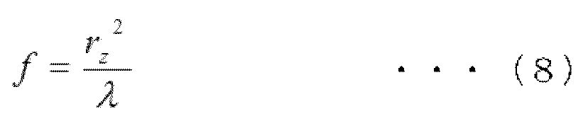
- the focal length f is expressed by Equation (8), where r z is the radius of the center of the zone plate, that is, the radius of the innermost ring zone.
- the region where the convergence size is smaller than half the aperture size is that the distance L between the diffraction grating and the sample is the zone. This is the case when it is longer than half the focal length f of the plate (L> f / 2).
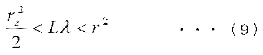
- the convergence size of the particle beam transmitted through the zone plate is smaller than half the maximum width of the opening area. . From this, conditional expression (9) is obtained.
- the particle beam transmitted through the zone plate can be focused on the sample.
- the intensity of the convergent beam is increased when the zone plate is not made of a transmittance of 0%, that is, made of a transmissive material.
- the intensity of the convergent beam is maximized and an increase of about 40% is obtained. Therefore, the material shown in Table 1 and the thickness of the film at that time are also effective in the zone plate.
- FIG. 6 shows a schematic diagram of a configuration example of the entire system of the particle beam apparatus according to the present embodiment.
- the apparatus shown in FIG. 6 is a charged particle beam apparatus 4 and assumes a general-purpose electron microscope having an acceleration voltage of about 100 kV to 300 kV. Therefore, an irradiation optical system is provided on the upper side of the sample, that is, on the upstream side in the direction of flow of the particle beam, and an imaging optical system is provided on the lower side of the sample, that is, on the downstream side of the direction of flow of the particle beam.
- the interference optical system described in detail in FIG. 6 in mind, the entire system with a biprism device is schematically depicted.
- the configuration of the interference type electron microscope as a charged particle beam device is listed in this example because not only the development of the interference electron microscope as the most complicated system among particle beam devices but also the method of using the device This is because it has versatility. For example, if all the lenses of the irradiation optical system are turned off in the system of the charged particle beam apparatus 4 in FIG. 6, the sample is directly irradiated with the electron beam from the particle source, and if the imaging optical system is also turned off, The simplest electron diffraction device. That is, the apparatus can be configured as a form simulating a neutron beam apparatus, a heavy particle beam, or an X-ray apparatus. However, application of this embodiment is not limited to the interference electron microscope having the configuration of FIG.
- the electron gun 1 which is a particle source is positioned at the most upstream portion in the direction in which the electron beam flows, and the emitted electron beam is controlled by the particle beam control unit 19 and the acceleration tube control unit 49.
- the light After accelerating to a predetermined speed at 40, the light is adjusted to a predetermined intensity and irradiation region through the condenser lenses 41 and 42 of the irradiation optical system controlled by the control units 47 and 48, and is applied to the diffraction grating 36 above the sample. Irradiated. Then, the transmitted wave and the diffracted wave transmitted through the diffraction grating 36 (not shown) are applied to the sample 3.
- the electron beam transmitted through the sample 3 is imaged by the objective lens 5 controlled by the control unit 59.
- This image forming action is taken over by the image forming lens systems 61, 62, 63, 64 controlled by the control units 69, 68, 67, 66 subsequent to the objective lens 5, and finally observed and recorded by the electron beam apparatus.
- the final image 8 is formed on the surface 75.
- the image passes through an image detector 79 such as a CCD camera and an image data controller 78, and is observed on the screen of an image data monitor 76 or stored as image data in an image data recording device 77, for example.
- FIG. 6 illustrates the case shown in FIG. 2B, that is, the case where the crossover is located between the diffraction grating and the sample.
- the biprism device 9 controlled by the control unit 98 performs drawing based on the most basic electron beam interference optical system disposed below the objective lens 5 and above the first imaging lens 61.
- the position of the biprism device 9 is not limited to between the objective lens 5 and the first imaging lens 61.
- the electron beam interference portion, that is, the superimposing portion by the biprism device 9 is magnified by the imaging lens systems 61, 62, 63, and 64 at the latter stage of the objective lens together with the sample image and imaged on the observation recording surface 75.
- the bipyrism device can be provided in either the objective lens system or the imaging optical system, or both.
- control unit 38 of the diffraction grating 36, the control unit 39 of the sample 3, the control unit 47 of the second irradiation lens 42, the control unit 48 of the first irradiation lens 41, the control unit 49 of the accelerating tube 40, and the objective lens 5 are used.
- Control unit 59 fourth imaging lens 64 control unit 66, third imaging lens 63 control unit 67, second imaging lens 62 control unit 68, first imaging lens 61 control unit 69, image Control units such as the control unit 78 of the detector 79 and the control unit 98 of the biprism device 9 are controlled.
- the electron gun 1, the acceleration tube 40, the lens, the sample 3, the diffraction grating 36, biprism device 9 can be controlled and the image detector 79.
- Example 2 is an example of a medical application apparatus using X-rays, heavy particle beams, or the like.
- radiation therapy such as cancer
- irradiation for the purpose of searching or observing the affected part, and irradiation for the purpose of treating the affected part found by the search May use the same radiation.
- the affected area is detected by irradiating a weak and wide area, and then a strong particle beam is irradiated at the pinpoint. .
- the strong particle beam irradiation is performed on the assumption that the observation result in the previous search is reproduced with the same accuracy.
- the present embodiment it is possible to perform radiation therapy while performing a search and observation of the affected part as the sample 3. That is, irradiation is performed with a transmitted wave portion that is a uniform and weak particle beam that passes through the irradiation region 37, and the entire image is observed.
- the affected part discovered there is used for treatment by irradiating the diffracted wave 22 from the opening region 35 at a pinpoint. This makes it possible to strongly irradiate the target site while observing the whole image, so that it is not necessary to search for an error or a position again, and as a result, the overall exposure dose can be reduced.
- the irradiation position is controlled by horizontal / vertical movement of the grid.
- the diffraction grating 36 can be attached to and detached from the optical system, and the irradiation dose can be further reduced by reducing the transmittance of the grating to be inserted after finding the affected part.
- the irradiation amount can be more appropriately reduce the irradiation amount by superimposing a shadow portion 21 of a zero-order diffracted wave that is a transmitted wave.
- the configuration of the present embodiment can be applied not only as a treatment for a patient as a subject but also to cell level research if the size of the entire system is reduced.
- This cell level treatment target is shown as sample 3 in FIG.
- Example 3 an example in which the electromagnetic field introduced directly by the particle beam into the sample with the same configuration as the basic configuration and apparatus configuration described in Example 1 will be described.
- the magnetic sample is irradiated with a target shape and size by the density of the irradiation probe under uniform illumination, and the effect of the magnetic development by irradiation can be controlled.
- Control of the position of the superimposed irradiation by the diffracted wave is based on the movement of the diffraction grating in the two-dimensional direction perpendicular to the optical axis of the device as described in the first embodiment. It can also be realized by moving in the axial direction.
- an electromagnetic phenomenon introduced into a material by light irradiation such as a magneto-optical material or a photo-dielectric material.
- Light waves can be controlled with an optical bench, etc., with a much higher degree of freedom compared to electron beams and other particle beams.
- the handling environment is limited to electron beams and other particles. The situation is similar to particle beams. Therefore, the present invention can be an effective observation means even in these photoinduced phenomena.
- a circular magnetization state similar to skyrmion can be created in the magneto-optical material by irradiation with a small probe, and if the size of the irradiation probe is slightly increased, a single domain structure Or, it can create an inverted two-domain structure. Furthermore, as the irradiation area becomes larger, a multi-domain structure can be created. According to the present embodiment, the created magnetic state and magnetic domain structure can be directly observed with the irradiation probe used. Such magnetic control not only leads to the elucidation of the elementary process of the magnetization phenomenon of the magnetic material as a physical phenomenon, but is also useful for processing of a magnetic semiconductor memory or for controlling operation.
- the dielectric material can be implemented in the same manner as the magneto-optical material and the same dielectric phenomenon can be observed, which can contribute to the elucidation of the elementary process of the electromagnetic phenomenon resulting from the particle beam irradiation and the observation of the organic thin film.
- Example 4 even in materials other than magnetic materials, an electromagnetic phenomenon that particle beams directly introduce into a sample material can be observed with the same configuration as the basic configuration and apparatus configuration described in Example 1.
- An example will be described. For example, in a non-hole type phase plate that has begun to be used in a transmission electron microscope, a high-density electron beam that is transmitted through a sample and converged by an objective lens itself is introduced into the carbon thin film by an electric field. It is estimated that the phase plate effect is obtained by changing the phase.
- the phase plate effect means that a phase wave of ⁇ / 4 is given between a transmitted wave, that is, a zero-order diffracted wave and a diffracted wave transmitted through the periphery of the phase plate, and the transmitted wave and the diffracted wave at that time
- the effect of this interference is to obtain a linear contrast in the phase distribution.
- the electron beam as a probe must be converged, but when it is converged, there is no electron beam in the surrounding area, and the phase difference cannot be determined, so the measurement itself can be performed. Absent. That is, the phase plate cannot be directly tested and evaluated in an environment where the phase plate is used.
- phase plate is considered to be an effective means for observing samples such as biological samples and dielectric samples that cannot be contrasted with an electron beam, but there is no direct method for evaluating the phase plate.
- the development of is a trial and error situation.
- the electromagnetic phenomenon itself in which the particle beam is introduced / expressed in the sample is general, and according to the configuration of the present embodiment, these general It is possible to provide an effective means for observing the electromagnetic phenomenon directly introduced by the particle beam in the sample material.
- Example 5 is an example of an optical system that superimposes a spiral wave on a sample.
- a spiral wave is superimposed on the sample. It can be used as an irradiating optical system.
- Spiral waves are a new particle beam that is considered to be the next-generation or next-generation probe, especially in the field of electron beams. This name is given because the equiphase surface has a spiral structure.
- a helical wave When a helical wave is generated by a charged particle beam, it may become a particle beam that propagates with magnetism. Detection of magnetization components in the direction perpendicular to the optical axis, observation of helical structures such as proteins, or magnetic properties It is thought that it becomes an effective particle beam for processing using.
- a uniform illumination particle beam that has passed through the outer periphery of the opening of the diffraction grating for observation on the sample, and a magnetic observation spiral, for example.
- a predetermined sample can be irradiated with waves simultaneously.
- Control of the position of the spiral wave can be realized by moving the diffraction grating in a two-dimensional direction perpendicular to the optical axis of the device, so the position of the magnetic material can be pinpointed while observing the entire sample image, or spiral.
- Magnetism can be imparted by waves.
- the above-described magnetic substance is replaced with a protein having a helical structure, position analysis of the targeted protein in the biological sample can be realized. Furthermore, if it demonstrates above, it can use also for processing of a material by adjusting the intensity
- Example 6 is an example of a particle beam apparatus that realizes application to an interference measurement method.
- FIG. 8 is a schematic diagram showing one configuration of the optical system of the particle beam apparatus according to the sixth embodiment. Specifically, this is an example of an interference optical system using a biprism apparatus with a transmission electron microscope in mind.
- the incident particle beam 25 irradiates the irradiation region 37 in a wider range than the opening region 35 of the diffraction grating 36 that retains the transmittance, and the ⁇ first-order diffracted wave 22 and the transmitted wave that are diffracted by the opening that is the opening region 35. 21 is superimposed and irradiated on the sample or the sample surface 3.
- the intensity of the transmitted wave that has passed through the aperture region 35, that is, the zero-order diffracted wave is reduced by the amount of energy applied to the diffracted wave, and the entire irradiated area on the sample or the sample surface 3 is irradiated. Create a shadowed area with reduced intensity.
- the intensity of the particle beam that has passed through the outer periphery of the opening of the diffraction grating 36 in the particle beam irradiation region 37 is used as a reference, and the intensity is increased by the amount of superposition of the diffracted wave from the reference.
- Three types of irradiation can be obtained simultaneously for the region and the region where the intensity is reduced by the amount of intensity applied to the diffracted wave.
- This biprism device 9 performs drawing with the electric field type electron biprism in an electron microscope in mind, and includes two filament electrodes 91 and a filament electrode 91 sandwiched between the optical axis 2 of the particle beam device.
- the parallel plate ground electrode 99 is used.
- FIG. 8 exemplifies an interference optical system in which a biprism device 9 is inserted below the sample or sample surface 3 and above the objective lens 5.
- This interference optical system has the advantage of being able to observe a wide range of interference region 82 at a low magnification, and is different in positional relationship from the optical system in which the biprism device 9 is arranged below the objective lens 5 shown in FIG.
- the interference optical system remains unchanged, and the present invention is not limited to any interference optical system.
- the objective lens 5 is focused on the sample or the sample surface 3, and an image of the sample is formed on the image surface 34.
- This sample image includes a region where two diffracted waves 22 are superimposed and a shadow region 21 of the diffraction grating on the optical axis 2 of the apparatus. Since the two diffracted wave superimposing areas are strong irradiation areas compared to other reference areas, if an electromagnetic phenomenon such as charging occurs inside the sample in the strong irradiation area or on the sample surface. The phenomenon is reflected as a phase change in the transmitted wave of the reference irradiation.
- FIG. 8 shows the configuration of an interference optical system for measuring the phase change.
- the azimuth rotation of the diffraction grating or the bi-prism device and the voltage applied to the filament electrode may be adjusted so that the interference area, that is, the hologram area includes the overlapping portion of the diffracted wave.
- any one or more of the diffraction grating holding device, the sample holding unit, and the biprism device are configured to be capable of azimuth rotation with the optical axis as the rotation axis.
- the arrangement direction of diffraction spots which is the direction in which diffraction occurs, is drawn from the upper right to the lower left with the optical axis 2 as the center. Further, the direction of interference by the biprism device 9, that is, the direction perpendicular to the interference fringes 84 is drawn from the upper left to the lower right in the figure.
- Example 7 is an example of an electron microscope and its observation method when coherence is maintained between the transmitted wave from the diffraction grating and the diffracted wave.
- holography can be realized using either the transmitted wave or the diffracted wave as the object wave and the other as the reference wave.
- electron beam holography can be realized without using the electron beam biprism described in the sixth embodiment.
- FIG. 9 shows the state of interference between the transmitted wave 21 and the diffracted wave 22 according to this embodiment.
- the diffraction grating 36 to be inserted is an edge dislocation grating 45 for generating a spiral wave, and diffraction is performed.
- the ring-shaped diffraction spot 26 will be described as the wave 22, the following description is not limited to the case where a spiral wave is used.
- the position (height) on the optical axis 2 that connects the crossover 26 is the same for the wave that has passed through the portion of the edge dislocation grating 45 that has been engraved and the wave that has been diffracted by the edge dislocation grating 45. .
- the crossover 26 surface is an image surface of the light source and corresponds to the diffraction surface 301 which is an inverse space for the diffraction grating 36. Therefore, when the diffraction grating 36 is an edge dislocation grating 45 for generating a helical wave, a ring-shaped diffraction spot 26 is generated in addition to the transmitted wave spot 26 as will be described in detail later with reference to FIG.
- the incident wave 25 that irradiates a wider area than the edge dislocation grating 45 has a large convergence angle.
- the incident wave 25 is rapidly reduced after passing through the edge dislocation grating 45 and is reflected on the diffraction surface 301. Tie spots. Then it expands rapidly.
- the diffracted wave 22 is also reduced by propagation, and is expanded after connecting the diffraction spot 26 of the minimum size on the diffractive surface 301.
- the degree of change in the size of the diffracted wave 22 is much smaller than that of the transmitted wave 21.
- the distance from the diffractive surface 301 is appropriately selected and a defocus surface is created, the space where the transmitted wave 21 and the diffracted wave 22 overlap can be observed.
- the transmitted wave 21 and the diffracted wave 22 are spatially within a coherent distance range, the interference of these two waves is observed.
- FIG. 10 shows an observation example of the change in size between the transmitted wave 21 and the ⁇ first-order and ⁇ second-order diffracted waves 22 due to the change in the position on the optical axis 2.
- FIG. 10A is a diffraction pattern, that is, an observation image when focused on the diffraction surface 301, and an image observed by increasing the amount of defocusing in the order of FIGS. 10B and 10C.
- FIG. 10A shows a pattern on the diffractive surface 301 of the edge dislocation grating 45, and a total of four diffraction spots of ⁇ 1st order and ⁇ 2nd order are arranged symmetrically about the transmitted wave spot 260 as a center. ing.
- the first-order diffraction spot 261 and the second-order diffraction spot 262 are arranged in order from the spot 260 of the transmitted wave.
- Each of the diffraction spots 261 and 262 is a ring-shaped diffraction spot characterizing a spiral wave.
- the bright disc-shaped region 263 in the center of FIGS. 10B and 10C shows a state where the beam spreads when the transmitted wave is out of focus from the diffraction surface, and this out-of-focus disc A slightly dark contrast portion at the center of the shape is the shadow 264 of the diffraction grating. Since the transmitted wave 21 spreads rapidly when it slightly deviates from the diffractive surface, the size of the disk-shaped bright region 263 increases rapidly according to FIGS. 10B and 10C and the amount of defocusing. On the other hand, the diffraction spots 261 and 262 are not greatly changed in size through (a), (b), and (c) of FIG. Thereby, individual interference between each diffraction spot and the transmitted wave can be observed.
- FIG. 10B and 10C the diffraction spots 261 and 262 overlap with the transmitted wave, and vertical stripes 84 are observed in the ring-shaped diffraction spots 261 and 262.
- FIG. The fringes 84 are interference fringes between the transmitted wave and the respective diffracted waves (spiral waves), and the diffraction spots 261 and 262 on which the vertical stripes 84 are superimposed are holograms of the respective spiral waves.
- the ring-shaped diffraction spots 261 and 262 in FIGS. 10B and 10C are not clearly visible because the intensity of the central portion is weak, the edge-shaped dislocation grating shown in FIG. Interference fringes with similar edge dislocations.
- fringes 265 that appear concentrically around the widened transmission spot 260 in FIGS. 10B and 10C are generated by superposition of Fresnel diffraction waves generated from the edge of the condenser aperture of the irradiation optical system. Fresnel stripes.
- FIG. 11 shows a reproduction image when the ⁇ 1st-order diffraction spot of FIG. 10C is cut out as a hologram and reproduced by the Fourier transform reproduction method.
- 11A shows the hologram of the ⁇ 1st order diffraction spot 261 on the left side of FIG. 10 and its reproduction amplitude image (Amplitude) and reproduction phase image (Phase), and
- FIG. 11B shows the + 1st order diffraction spot on the right side.
- 261 shows a hologram 261 and its reproduction amplitude image and reproduction phase image.
- the phase distribution 846 of the reproduction phase image is reproduced so as to be folded back every 2 ⁇ .
- the reproduced phase image clearly shows that the diffracted wave is a topological number 5 helical wave.
- the amplitude image reproducing the ring shape 845 it can be seen in FIG. 11 that the spiral wave has been successfully reproduced.
- FIG. 12 shows the interference optical system when the observation of FIG. 10 of the present embodiment is realized and the hologram of FIG. 11 is recorded.
- the crossover 26 on the upstream side of the edge dislocation grating 45 in the direction in which the electron beam flows is used as the diffraction surface 301, and the positions of the underfocus surface 302 and the overfocus surface 303 therebelow are recorded. is doing. This corresponds to observing a virtual image for the edge dislocation grating 45, but for the optical system, it is in a conjugate relationship with the optical system described in FIG. 9, and is equivalent.
- the observation example of the experimental result in FIG. 10 is based on the optical system in FIG.
- the optical system of FIG. 12 has no problem as an optical system for this embodiment, and it is easy to obtain a longer camera length.
- the holographic optical system according to the eighth embodiment in which the diffracted wave 22 is configured as an object wave and the transmitted wave 21 is configured as a reference wave.
- An example is shown.
- a configuration in which the diffracted wave 22 is a reference wave and the transmitted wave 21 is an object wave is also possible.
- illustration is omitted, for example, when the sample 3 is a fine particle or the like, the sample 3 is arranged in a part of the transmitted wave, and the projected image of the fine particle is made to coincide with the overlapping region of the diffracted wave 22 and the transmitted wave 21, thereby diffracting.
- the edge dislocation grating 45 which is a diffraction grating in the traveling direction of the incident particle beam 25 which is a charged particle beam, and the sample 3 placed on the diffraction surface 301 of the edge dislocation grating 45 are arranged. Configured in order.
- the sample 3 to be observed is placed on the diffractive surface 301 that is an inverse space for the edge dislocation grating 45, and the diffracted wave 22 and transmitted wave 21 that are spiral waves that pass through the sample 3. Is recorded by shifting the position from the diffractive surface 301 along the optical axis 2 either up or down (out of focus when the diffractive surface 301 is used as a reference).
- the transmitted wave 21 is a reference wave
- the spiral wave (diffracted wave 22) is transmitted through the sample 3 as an object wave.
- the diffraction spot 26 of the spiral wave is transmitted through the sample 3, and the hologram is recorded on the underfocus surface 302 or the overfocus surface 303.
- the object to be observed may be an electromagnetic field existing in space or a strain field inside a substance. Any object that modulates the phase of the electron wave can be observed. These are collectively referred to as samples.
- the interference measurement with a spiral wave using the edge dislocation grating 45 has been described from the viewpoint of easy illustration of the diffraction spot on the diffraction surface.
- the present embodiment is not limited to the spiral wave. .
- holography can be realized.
- electron beam holography can be realized without using an electron beam biprism.
- irradiation of the sample with the irradiated particle beam superimposed or reduced by diffraction based on the irradiation amount by the particle beam transmitted without being diffracted by the diffraction grating It is possible to provide a particle beam apparatus capable of observing the influence of the above along with the state of the peripheral portion, and an observation method thereof.
- the various embodiments described above have been described for better understanding of the present invention, and are not necessarily limited to those provided with all the configurations described above.
- the outer peripheral portion of the opening area of the diffraction grating does not exist around the entire opening area, and may be arranged only in part.
- a part of the configuration of one embodiment can be replaced with the configuration of another embodiment, and the configuration of another embodiment can be added to the configuration of one embodiment.
- a plurality of diffraction gratings are arranged in the irradiation region of the incident particle beam, so that a plurality of locations using diffraction waves from the respective diffraction gratings are arranged. It is also possible to perform simultaneous superimposing irradiation. At this time, if the aperture shape of the diffraction grating, the grating pattern and the like can be arbitrarily changed as parameters, a more complicated pattern can be superimposed and irradiated according to the situation of the irradiation target. For example, if it is a medical application like Example 2, it will become possible to control and irradiate a particle beam to the shape according to the affected part of a patient, and required intensity
- control unit has been described using an example of a system control computer in which a program that realizes a part or all of them is used. It goes without saying that it may be realized by hardware by designing or the like. That is, all or part of the functions of the control unit may be realized by an integrated circuit such as ASIC (Application Specific Integrated Circuit) or FPGA (Field Programmable Gate Array) instead of the program.
- ASIC Application Specific Integrated Circuit
- FPGA Field Programmable Gate Array
- Electron gun or particle source 18 Vacuum container 19 Particle source control unit 2 Optical axis 21 Transmitted wave 22 Diffraction wave 23 Irradiation region 25 Incident particle beam 26 Crossover 260 Spot 261, 262 Diffraction spot 263 Bright region 264 Shadow of shadow 265 Stripe 3 Sample or sample surface 30 Substrate 301 Diffraction surface 302 Underfocus surface 303 Overfocus surface 31 Trunk portion 32 Thin film 33 Reinforcement portion 34 Sample image or sample image surface 35 Aperture area 36 Diffraction grating 37 Particle beam irradiation area 38 Diffraction grating Control unit 39 Sample control unit 4 Charged particle beam device 40 Accelerating tube 41 First condenser lens 42 Second condenser lens 43 Simple lattice 44 Zone plate 45 Edge dislocation lattice 46 Vortex zone plate 47 Control of the second condenser lens Unit 48 First condenser lens control unit 49 Acceleration tube control unit 5 Objective lens 51 System control computer 52 System control computer monitor 53 System control computer interface
Landscapes
- Chemical & Material Sciences (AREA)
- Analytical Chemistry (AREA)
- Physics & Mathematics (AREA)
- General Physics & Mathematics (AREA)
- Health & Medical Sciences (AREA)
- Life Sciences & Earth Sciences (AREA)
- Biochemistry (AREA)
- General Health & Medical Sciences (AREA)
- Immunology (AREA)
- Pathology (AREA)
- Optics & Photonics (AREA)
- High Energy & Nuclear Physics (AREA)
- General Engineering & Computer Science (AREA)
- Engineering & Computer Science (AREA)
- Analysing Materials By The Use Of Radiation (AREA)
- Diffracting Gratings Or Hologram Optical Elements (AREA)
Abstract
回折効果を利用し、同一視野内に二つの光学状態による粒子線照射の粗密を作り出す。試料3上側、照射光学系の下側に粒子線を透過する材料で製作された回折格子36を配置し、回折格子36の開口領域35よりも広範囲な領域37を粒子線25が照射するように構成する。開口領域35によってブラッグ回析された粒子線と、開口領域35の外側周辺部を回折を受けずに透過した粒子線を重畳して試料3に照射することによって、試料3へ照射される粒子線の粗密を作りだすことが可能となる。
Description
本発明は、回折効果を利用する粒子線装置とその観察法、及びそれに利用する回折格子に関する。
電子線やイオンビームなどの荷電粒子線は、真空中を伝搬させなければならないこと、波長が数pmの桁と短く、偏向角度が小さいこと、光学におけるハーフミラーの様な有効なビームスプリッターがないことなどから、光学ベンチにおけるマッハツェンダー干渉計のごとく複数の光学経路を作り出してそれぞれ独立に光学系を構成することは難しい。また、紫外線やX線など短波長の電磁波では、その良透過性から有効な光学素子を構成することが難しく、さらには中性子線や分子線・重粒子線などの粒子線ではそもそも光学素子がない。そのため、光源から検出器までの間に試料を配し、経路伝搬による試料での散乱・吸収像の観察か、あるいは干渉・回折効果に基づく回折パターンの観察が実施されているのみである。すなわち、上記いずれの電磁波装置、粒子線装置においても、1経路の光学系が用いられており、試料を透過した透過ビームにも散乱・回折ビームにも同一のレンズや同一の偏向器などを用いなければならず、同一の光学条件を適用した計測法が用いられている。
上記装置類の中では、電子線を用いた電子顕微鏡が最も開発が進んでおり、電子レンズ、偏向器、電子線バイプリズムなど様々な光学素子が実現されているが、原理的に電子線の伝搬は真空中でなければならず、1つの真空排気された鏡筒内に1経路の光学系で構成されているのみである。電子線干渉において唯一有効なビームスプリッターである電子線バイプリズムを利用した場合でも、その偏向角度は最大でも10-3 radと小さく、2つの経路に対して、同一のレンズ、偏向器を用いなければならないという制約は、他の粒子線装置類と何ら変わらない。そのため、同一視野内に電子線照射の粗密を作り出すことは難しく、電子線照射に起因した試料の帯電効果や試料損傷の程度を2つの照射条件を同時に比較参照しながら観察すること、とりわけその変化の過程を観察することは困難であった。
上記課題に対する対策ではないが、フーリエ変換ホログラフィーとして、1鏡筒内に2つの照射条件を作り出す手法を開示する非特許文献1と、X線で2つの照射条件を作り出す可能性を開示した特許文献1がある。
非特許文献1は、アモルファス薄膜からなる拡散板を透過した電子線の対物レンズの後焦点面を試料面として利用する手法で、拡散板で散乱を受けずに透過した電子線は光軸上にスポットを結び、アモルファス膜でランダムに散乱された電子線は後焦点面で平面上に広がる現象を利用したもので、光軸上のスポットと平面状部分の電子線との干渉を利用する。特許文献1は非特許文献1の拡散板に変わり、孔を設けたゾーンプレートを利用するもので、ゾーンプレートのレンズ効果による焦点がスポットとなり、孔を透過したX線が平面波となる。いずれの例もホログラフィーとしては実用的でなく普及していない。また、レンズの存在しない粒子線装置では、実現不可能な構成である。
また、試料の上側に回折格子として刃状転位格子(フォーク型格子)を配置する例は特許文献2、3に開示されている。特許文献2は刃状転位格子を透過し、逆空間においてらせん波となった回折電子線のみを試料に照射するもので、刃状転位格子と試料との間には電子レンズと絞り孔を備え、その後焦点位置に試料を配置する。この例もレンズの存在しない粒子線装置では実現不可能である。
R. Lauer; Optik, 67 (1984) 291.
上述したように、紫外線やX線などの短波長の電磁波装置や粒子線装置では1経路の光学系、すなわち、試料を透過した透過ビームにも散乱・回折ビームにも同じレンズや同じ偏向器など同一の光学条件を適用した計測法しか利用できないため、同一視野内に2つの光学状態による粒子線照射の粗密を作り出すことは難しく、広範囲を照射しながら、局所的に照射量を増やして明るさを稼ぎ高倍率観察すること、あるいは局所的な試料状態の照射量依存性を、周辺部を参照してその変化を観察すること、また加工などにおいては、全体を一定の低量照射しながらピンポイントに局所高密度照射を施し、加工・調整などを実施することは困難であった。
例えば電子線照射における試料の帯電効果の観察は、帯電しない試料中に一部絶縁体を配置し、観察時の照射電子線による絶縁体部のチャージアップ現象を観察する。もしくは、電子線をスポット状に絞り電流密度を高くして試料の一部を照射し、後に照射領域を広げてスポット照射部の帯電の変化の様子を事後に観察するのみであった。すなわち、電子線がおのずから導入する直接的な照射効果を平衡状態で観察する手法はなかった。これは帯電現象の観察手段と導入手段がいずれも同じ電子線であるためで、回避不可能と考えられていた。
本発明の目的は、上記の課題を解決し、同一視野内に二つの光学状態による粒子線照射の粗密を作り出すことが可能な粒子線装置、その観察法、及び回折格子を提供することにある。
上記の目的を達成するため、本発明においては、粒子線装置であって、粒子線を発生する粒子線源と、粒子線を試料に照射する照射部と、試料を保持するための試料保持部と、試料を透過した粒子線を取得するための検出部と、照射部における粒子線の進行方向下流側で、試料の粒子線の進行方向上流側に備えられ、粒子線に対して透過性を有する材料で構成される回折格子と、回折格子の当該装置の光軸上への着脱と移動を可能とする保持装置とを備え、回折格子の開口領域は粒子線の回折格子への照射領域よりも小さい構成の粒子線装置を提供する。
また、上記の目的を達成するため、本発明においては、荷電粒子線装置よる観察法であって、荷電粒子線装置は、荷電粒子線を発生する光源と、荷電粒子線を試料に照射する照射部と、試料を保持するための試料保持部と、試料を透過した荷電粒子線を結像する少なくも一つのレンズからなる対物レンズ系と、対物レンズ系の荷電粒子線の進行方向下流側に配置された複数のレンズからなる結像光学系と、照射部における荷電粒子線の進行方向下流側で、試料の荷電粒子線の進行方向上流側に備えられ、荷電粒子線に対して透過性を有する材料で構成される回折格子とを備え、回折格子の開口領域を、荷電粒子線の回折格子への照射領域よりも小さくし、試料上に作られる回折格子により回折された荷電粒子線の照射領域が、回折格子を透過した荷電粒子線の照射領域内にある状態を観察する観察法を提供する。
更に、上記の目的を達成するため、本発明においては、粒子線装置に用いる回折格子であって、粒子線に対して透過性を持つ材料で構成され、粒子線を回折する開口領域と当該開口領域の外側周辺部とを有し、粒子線を開口領域及び外側周辺部に照射したとき、粒子線が流れる方向の下流側に設置される試料に照射される粒子線の粗密を形成する回折格子を提供する。
本発明によれば、回折格子で回折を受けずに透過した粒子線による照射量を基準にして、回折により重畳あるいは減少された粒子線による試料への照射の影響を、周辺部の様子とともに観察可能となる。
以下、本発明を実施するための形態を説明するに先立ち、本発明の原理手法を概説する。試料面に置かれた試料の上側、照射光学系の下側に、例えば電子線などの粒子線に対して透過性を有する基板に構成される回折格子を配置し、回折格子の開口領域よりも広範囲の照射領域を粒子線が照射すると、回折格子によってブラッグ(Bragg)回折された照射ビームと、回折を受けなかった透過ビームとが重畳して試料に照射されることによって、試料への照射ビームの粗密を作り出すことができる。
このとき、回折格子の光軸垂直方向の位置変更により試料面上の重畳照射される照射位置の制御が可能であり、照射ビームが収束照射、あるいは拡散照射の場合には、回折格子の光軸方向の位置変更により試料面上に重畳照射される照射スポットサイズが制御可能である。この手法は、ブラッグ回折のみに基づいているため、ブラッグ回折する程度の干渉性を持つ粒子線であれば、X線等の電磁波や電子線・イオンビームなどの荷電粒子線だけでなく、分子線・重粒子線や中性子線などでも実施可能である。
上記の手法によれば、回折格子の開口領域での回折を受けず、回折格子の開口外側周辺部を透過した透過ビームによる照射量を基準にして、その照射領域内に回折格子によって回折された回折ビームを重畳付加することが可能となる。さらに、回折格子の開口領域の影の部分は回折ビームとして使われた分照射ビームが減少するため、基準照射量よりも減少した場合についても、同時観察が可能である。すなわち重畳あるいは減少された粒子線による試料への照射の影響を、周辺部の様子とともに観察可能となる。
また、回折ビームによる重畳照射位置を、透過ビームにより均一照射された周辺部を参照して干渉観察することが可能で、試料への粒子線の局所照射による効果のみを計測することができる。この時、回折ビームの回折方位と2波を重畳干渉させる干渉方位を直交させることが可能であり、重畳された回折ビームの影響を干渉に寄与させず、高精度計測が可能である。さらに、回折格子を照射する照射角と格子の回折角、および格子と試料との距離により、照射ビームの可干渉性の制御も可能である。すなわち、本発明による光学系は、干渉計測においても高い自由度、制御性を有している。
以下の明細書の記載、及び特許請求の範囲の記載において、粒子線装置とは、中性子線や分子線・重粒子線などの粒子線装置だけでなく、電子線やイオンビームなどの荷電粒子線を用いる装置と、さらにX線や紫外線、ガンマ線などの電磁波を用いる装置を総称するものとする。また、電子線、イオンビームなどの荷電粒子線、分子線・重粒子線や中性子線、更にはX線等の電磁波を含め、波動を伴いブラッグ回折する程度の干渉性を持つビームを粒子線と総称するものとする。また、回折格子とは、粒子線を回折する開口領域と当該開口領域の外側周辺部を含めた素子、すなわち物体としての回折格子を意味するものとする。
実施例1は回折効果を利用する粒子線装置とその観察法、及びそれに利用する回折格子の実施例である。すなわち、粒子線を発生する粒子線源と、粒子線を試料に照射する照射部と、試料を保持するための試料保持部と、試料を透過した粒子線を取得するための検出部と、照射部における粒子線の進行方向下流側で、試料の粒子線の進行方向上流側に備えられ、粒子線に対して透過性を有する材料で構成される回折格子と、回折格子の当該装置の光軸上への着脱と移動を可能とする保持装置とを備え、回折格子の開口領域は粒子線の回折格子への照射領域よりも小さい構成の粒子線装置の実施例である。
また、荷電粒子線装置よる観察法であって、荷電粒子線装置は、荷電粒子線を発生する光源と、荷電粒子線を試料に照射する照射部と、試料を保持するための試料保持部と、試料を透過した荷電粒子線を結像する少なくも一つのレンズからなる対物レンズ系と、対物レンズ系の荷電粒子線の進行方向下流側に配置された複数のレンズからなる結像光学系と、照射部における荷電粒子線の進行方向下流側で試料の荷電粒子線の進行方向上流側に備えられ、荷電粒子線に対して透過性を有する材料で構成される回折格子とを備え、回折格子の開口領域を、荷電粒子線の回折格子への照射領域よりも小さくし、試料上に作られる回折格子により回折された荷電粒子線の照射領域が、回折格子を透過した荷電粒子線の照射領域内にある状態を観察する観察法の実施例である。
図1に本発明の光学系の基本構成、並びに実施例1に係る粒子線装置の最も基本的な構成を示す。粒子線装置において、試料もしくは試料面3よりも上流側に開口領域35を有する回折格子36が配され、回折格子36の開口領域35を透過した透過波21と回折した回折波22が試料もしくは試料面3をそれぞれ個別に照射している。回折格子36は、使用する粒子線25に対して透過性を持つ材料で作られた基板で作られており、粒子線25が回折格子36を照射する領域37は、開口領域35の開口サイズよりも大きくなるように構成されている。更に、回折格子36を透過した粒子線25が試料もしくは試料面3を照射する照射領域23は、回折格子により回折された回折波22が照射する位置、及びその領域よりも大きくなるように粒子線25は調整されている。
これにより、試料もしくは試料面3上を照射する粒子線25は、開口領域35を透過した粒子線である透過波21が照射する粒子線装置の光軸2を含む領域は、開口領域35の回折効果によって粒子線の強度が周辺部よりも減少している。また開口領域35により回折された回折波22が照射する試料もしくは試料面3上の粒子線は、領域37に対応する開口領域35の外側周辺部を透過した透過波と回折波22との合成されたものとなるため、その周辺部よりも強度が増している。
このように、粒子線に対して透過性を有する材料からなる基板で作られた回折格子36を用い、その開口領域35が粒子線の基板への照射領域37よりも小さくなるように構成することにより、試料面上には、回折格子36の開口領域35の外側周辺部を含む照射領域37に対応する透過粒子線と、透過性を有する基板に形成された回折格子36の開口領域35により回折された照射粒子線の回折スポット、及び回折格子の陰とが重畳されることにより、粗密が形成される。
本実施例の構成によれば、回折格子を透過した入射波が試料面上を照射する強度を基準とすると、装置の光軸上の回折格子の開口領域は回折格子の影の領域となり粒子線強度が減少し、回折波が到達した試料面上は透過波と回折波との重畳により、粒子線の強度が増している。このように、試料面の粒子線に対する上流側に回折格子を配置すると、3通りの照射強度を同一視野中に同時に作り出すことができる。
図1の基本構成において、回折格子36と試料3とは互いに独立で、それぞれ水平2次元方向と垂直方向に微動が可能なホルダーに設置されており、従来の粒子線装置と同様に試料の観察位置を定めることが可能である。さらに回折格子の位置を微動させることにより、その試料の任意の位置に回折波を重畳させる、あるいは回折格子の開口の陰の領域を重畳させることが可能である。回折格子と試料のいずれか一方、あるいはそれら両方のホルダーが、光軸と平行な軸を回転軸とする方位角回転の機構を持てば、試料3の観察位置と試料への回折波の重畳照射位置の選定に対して、より自由度が大きくなる。
さらに、回折格子と試料のそれぞれのホルダーは、独立して光学系内、装置の光軸上への着脱が可能な構成とすることにより、例えば回折格子を光学系の光軸上からはずした場合には従来の粒子線装置としての試料観察が可能である。また本実施例の構成を用いた観察法を実施する手順として、試料を光学系内に設置する前に回折格子だけを光学系内に設置し、回折波の重畳の状態を調整することも可能である。この手順は試料への粒子線の照射量を減らす上で有効な処置である。
なお、図1の照射光学系の基本構成は、回折格子36と試料もしくは試料面3との間に粒子線のクロスオーバー26を形成する場合を図示したもので、粒子線装置の照射光学系が収束ビームを作り出せる装置の場合、すなわち電子線装置やイオンビーム装置などの荷電粒子線装置に好適な構成例である。
以下、本実施例の粒子線装置におけるクロスオーバー26の位置について説明する。一般的にクロスオーバー26の位置は、図2の(a)に示す如く回折格子36の上側の場合、図2の(b)および図1に示す回折格子36と試料3との間に位置する場合、そして図2の(c)に示す試料もしくは試料面3の下側に位置する場合、の3通りが考えられる。
図2の(a)に示す照射光学系は、X線や中性子線、分子線など、プローブとして用いる粒子線を収束・発散させるのに十分な照射光学系、あるいは試料を観察できる結像光学系を持たない粒子線装置においては必須の光学系である。もちろん電子線装置、イオンビーム装置においても実施可能な光学系であり、試料もしくは試料面3上での透過波21が照射する基準照射領域と回折波22が重畳照射する領域、そして開口領域35の影の領域のそれぞれを広範囲とする場合に有効な光学系である。
図2の(b)は、回折格子36と試料もしくは試料面3との間で一度クロスオーバー26を作り透過波21、回折波22のそれぞれをスポットにするため、試料面上での透過波が照射する基準照射領域に対して相対的に小さな回折波が重畳照射する領域と回折格子の開口の影の領域を作る場合に有効な光学系である。また、図2の(c)は、図2の(a)と対を成す光学系であり、試料もしくは試料面3上での透過波が照射する基準照射領域と回折波が重畳照射する領域、そして回折格子の開口の影の領域のそれぞれを狭い範囲とする場合に有効な光学系である。
図2に示した3つの光学系、すなわちクロスオーバー26と回折格子36と試料3との位置関係は、有効なレンズ系を有する荷電粒子線装置では、必要に応じて簡単に使い分けることが可能である。X線装置、中性子線装置においても、弱いながらもレンズ系は考案されているので、粒子線の経路長さえ十分に長く取ることができれば、原理的には3つの光学系をそれぞれ実現可能である。
図3は本実施例の粒子線装置並びに観察法で用いる回折格子の一構成例を示す半断面図である。上述したように、回折格子は使用する粒子線に対して透過性を持つ材料からなる基板30で構成される。図3の(a)は基板30に構成され、格子の幹部31を有する単純格子、(b)は基板30に構成されたゾーンプレート、(c)は基板30に構成され、内側のリング部を保持するための薄膜32を格子下部に付加したゾーンプレート、(d)は補強部33により内側リング部を保持する型のゾーンプレートである。ゾーンプレートのように基板30に構成される格子部分が開口外側周辺部と独立するパターン形状の場合には、図3の(c)や(d)のような格子部を保持、補強する工夫が必要となる。薄膜32は、回折格子に照射される粒子線に対して透過性を有する材料で構成される。なお、図3はいずれも円形開口の場合を図示しているが、本実施例の構成は円形開口に限定するものではない。
図3の(a)の単純格子を例に説明するが、図3の(a)では回折格子36の幹部31と幹部31の隙間の空間部分を同じ幅で、かつ幹部31を矩形に描いている。幹部31の形状を矩形にすることにより、高調波として高次の回折波を発生させることが可能となる。そして、幹部31と幹部31の隙間の空間部分の幅の比により高次の回折波の強度を制御することができる。例えば、幹部31と幹部31の隙間の空間部分の幅の比が1:1の時には2次の回折波の強度を弱めることが可能であり、幹部31と幹部31の隙間の空間部分の幅の比が2:1、あるいは1:2の時には3次の回折波の強度を弱めることが可能である。また、幹部31の形状を正弦関数様に加工した場合には、回折波の高調波の発生を抑えることが可能で、±1次の回折波の強度を高めることも可能である。
図1と図2に示した通り本実施例の構成では、回折格子の開口領域、すなわち開口部の外側周辺部の基板30を透過した粒子線が照射強度の基準となる。そのため回折格子36を構成する基板30は、粒子線に対して透過性が100%である必要はないが、入射粒子線を十分な強度を持ったまま透過させられる程度の厚さに制限する必要がある。また、入射粒子線の干渉性は、実施例の中で述べる干渉光学系を想定する場合以外は必須ではないが、回折格子とその下流側の試料を透過した後の粒子線が結像できる程度には干渉性の劣化や非弾性散乱による入射粒子線のエネルギー散逸を低く抑える必要がある。その判断基準としては、例えば、回折格子を構成する基板あるいは薄膜の材料を透過した300kVの電子線が受ける位相変調をπ程度か、それ以下とするという条件を用いることができる。
表1に300kVの電子線へ位相差πを与えるときの基板の厚さを、いくつかの基板あるいは薄膜の材料について例示する。この中では、材料が市販されていて、かつ加工の容易性などから30nm厚、もしくは50nm厚の窒化シリコン(Si3N4)膜の利用が適切である。この時、Si3N4膜は絶縁性があるため、粒子線が電子線など荷電粒子線を用いる場合には、例えばカーボン(C)蒸着、あるいは白金パラジウム(PtPd)コーティング等により帯電防止策を付加することは必須である。
表1

表1
図4に本実施例の粒子線装置で用いることができる回折格子のいくつかの型を例示する。回折格子を薄い色で描画しているが、これは上述の回折格子を構成する基板あるいは薄膜が、用いる粒子線に対して透過能を持つ、すなわち透過性を有することを示すためである。図4の(a)は単純格子43、図4の(b)はゾーンプレート44、図4の(c)は刃状転位格子45、図4の(d)は渦状ゾーンプレート46である。図4の(a)、(b)は図3の(a)、(b)で示した回折格子と同種のもの、図4の(c)、(d)は、らせん波を発生させる回折格子である。らせん波は等位相面がらせん形状をしているため、らせんのコア部において位相が一意に定まらない特異点を持つ波で、軌道角運動量を保持したまま伝搬できる波と考えられており、例えば電子線などの場合には伝播方向に磁場を伴ったプローブとなる可能性がある(特許文献3参照)。
入射粒子線を図4の(c)に描いた刃状転位格子45を透過させた場合には、格子中央の刃状転位の部分を軸にらせん状の平面波を回折波として発生させる。また、図4の(d)の渦状ゾーンプレート46では、渦中央の刃状転位の部分を軸にした球面波状のらせん波を発生させる。当然のことながら、図4の(c)、(d)は回折格子としての特徴も持つため、先述した格子の幹と幹の隙間の空間部分の幅の比や格子の幹部の形状で、回折波の高調波を制御可能である。なお、図4で図示した例も開口形状を円形に描画しているが、本実施例の回折格子の開口領域である開口部は円形開口に限定するものではない。
次に図5を用いて、回折格子によるブラッグ回折と、本実施例の装置構成で利用する回折格子の適用条件について説明する。なお、数式の導出に当たっては、簡便のため直径2rの円形開口について述べるが、2rを開口の最大サイズとみなせば、他の開口形状についても同様に扱うことができる。また簡単のため、入射粒子線は平行ビームを仮定している。
ブラッグ回折とは、周期構造を持つ対象に対して入射した波動が対象を透過、あるいは反射する際にある特定の角度で強度が強くなる現象のことで、結晶に対するX線での現象として発見された。これは結晶を構成する原子により散乱されたX線が、結晶の周期構造により強めあったり打ち消されたりして発生する。X線の波長をλ’、結晶面の間隔をd’、結晶面とX線との成す角度をθ’、nを整数とすると、ブラッグ条件として式(1)で表される。

図5の(a)には、回折格子でのブラッグの関係を示している。ブラッグ条件は、回折格子の格子間隔をd、入射粒子線の波長をλ、回折角をθ、nを整数として式(2)で表される。

式(2)では、回折角θは微小角度として近軸近似を行っているが、本実施例の構成で取り扱う粒子線回折としては一般性を失わない。また、±1次の回折波について主に取り扱うためn=1とできる。さらに、回折現象を粒子線装置で観察するとき、試料と検出面との距離をL、検出面における透過波と回折波との距離をRとおくと、ブラッグ条件はまとめて式(3)に簡略化できる。

次に本実施例の装置構成で利用する回折格子の適用条件を説明する。上述の回折格子と検出面との距離Lを、図5の(b)に示すように、回折格子36を配した位置と、粒子線照射対象である試料もしくは試料面3の位置との間の距離Lとして置き直す。本実施例の構成の適用条件としては、回折格子36と試料もしくは試料面3との距離Lが実施の可否を判断する一つのパラメータとなる。回折格子を平行な照射波で照明したときの透過波と回折波との関係として、
(i) 透過波と回折波とが試料面上で重ならない、
(ii) 透過波が点像とならない(フラウンホーファー回折の条件に達しない)
の2条件を満たす必要がある。
(i) 透過波と回折波とが試料面上で重ならない、
(ii) 透過波が点像とならない(フラウンホーファー回折の条件に達しない)
の2条件を満たす必要がある。
(i)の条件は、回折格子の開口領域の最大幅よりも同じかより広い領域を粒子線が照射するとき、回折格子を透過した粒子線により形成される回折格子の陰の領域と回折格子により回折された粒子線とが、試料上で互いに重ならないことを意味する。
(i)の条件からは、回折波が回折角θにて距離Lだけ伝搬後、回折波の領域と透過波が作る格子の影の領域とが重なり合わない条件として式(4)が導かれる。

すなわち、回折格子の格子間隔と回折格子の開口領域の最大幅との積が、粒子線の波長と、試料と試料の粒子線が流れる方向の上流側に備えられる回折格子との距離との積よりも小なることを意味する。
また(ii)の条件は、フラウンホーファーの回折条件である式(5)を満たさない、として式(6)を得る。


すなわち、本実施例の構成を実現するにあたり、回折格子のパラメータ(d, r)と粒子線装置のパラメータ(L, λ)は、式(7)を満たせばよい。

式(7)で説明した適用条件は、図3の(a)や図4の(a)で示した単純格子43を用いる場合の条件であった。ここで、図3の(b)、(c)、(d)や図4の(b)に示したゾーンプレート44の場合についても説明する。ゾーンプレート44は、レンズと同様の収束効果を持っている。その焦点距離fは、ゾーンプレートの中心部の半径、すなわち一番内側の輪帯の半径をrzとして式(8)で表される。
ゾーンプレートの場合、開口に平行に入射した粒子線が焦点距離で点像に収束するため、収束サイズが開口サイズの半分よりも小さい領域であるのは、回折格子と試料との距離Lがゾーンプレートの焦点距離fの半分よりも長い場合(L>f/2)である。言い換えるなら、ゾーンプレートの開口領域の最大幅よりも同じかより広い領域を粒子線が照射するとき、ゾーンプレートを透過した粒子線の収束サイズが開口領域の最大幅の半分よりも小さい場合である。これより、条件式(9)を得る。
このゾーンプレートによれば、ゾーンプレートの開口領域の最大幅よりも同じかより広い領域を粒子線が照射するとき、ゾーンプレートを透過した粒子線が試料上に焦点を結ぶことができる。
なお、ゾーンプレートの透過率については、ゾーンプレートを透過率0%でない、すなわち透過性のある材料で構成すると、収束ビームの強度が増すことが知られている。特にゾーンプレートの中心部の一番内側の輪帯を透過する粒子線にπの位相変化を与えた場合には、収束ビームの強度は最大となり約40%の強度増加が得られる。そのため、ゾーンプレートにおいても表1で示した材料とその時の膜の厚さは同様に有効である。
図6に、本実施例に係る粒子線装置のシステム全体の一構成例の模式図を示す。図6の装置は荷電粒子線装置4であり、100kVから300kV程度の加速電圧を持つ汎用型の電子顕微鏡を想定している。そのため試料の上側、すなわち粒子線の流れる方向の上流側には照射光学系を、試料の下側、すなわち粒子線の流れる方向の下流側には結像光学系を備えており、さらに、実施例6で詳述する干渉光学系への展開を念頭に、バイプリズム装置を備えた場合のシステム全体を模式的に描いている。
荷電粒子線装置として干渉型の電子顕微鏡構成を本実施例に挙げたのは、粒子線装置の中では干渉型電子顕微鏡が最も複雑なシステムとして開発が進んでいるだけでなく、装置の利用手法においても汎用性を併せ持っているためである。例えば、図6の荷電粒子線装置4のシステムで照射光学系のレンズをすべてオフすれば、粒子源からの電子線を直接試料に照射する形態となり、合わせて結像光学系もオフすれば、最もシンプルな電子回折装置となる。すなわち、中性子線装置や重粒子線、X線装置を模擬する形態として装置を構成することができる。ただし、本実施例の適用を図6の構成を持つ干渉型電子顕微鏡に限定するものではない。
図6において、粒子源である電子銃1が電子線の流れる方向の最上流部に位置し、粒子線の制御ユニット19と加速管の制御ユニット49の制御により、放出された電子線は加速管40にて所定の速度に加速された後、制御ユニット47、48に制御される照射光学系のコンデンサレンズ41、42を経て、所定の強度、照射領域に調整されて試料上部の回折格子36に照射される。そして図示を省略した、回折格子36を透過した透過波と回折波は試料3に照射される。試料3を透過した電子線は、制御ユニット59に制御される対物レンズ5にて結像される。この結像作用は、対物レンズ5よりも後段の制御ユニット69、68、67、66に制御される結像レンズ系61、62、63、64に引き継がれ、最終的に電子線装置の観察記録面75に最終像8が結像される。その像はCCDカメラなど画像検出器79と画像データコントローラ78を経て、例えば画像データモニタ76の画面上で観察したり、画像データ記録装置77に画像データとして格納される。
回折格子36を透過した透過波と回折波は、光学系を介さずに試料3に照射されるが、光源の像の位置であるクロスオーバーの位置は、照射光学系によって任意に選択が可能である。図6は、図2の(b)に示した場合、すなわちクロスオーバーが回折格子と試料との間に位置する場合を描いている。
また、制御ユニット98に制御されるバイプリズム装置9は、対物レンズ5の下側で第1結像レンズ61の上側に配置する最も基本的な電子線干渉光学系に基づき描画している。もちろんバイプリズム装置9の位置は、この対物レンズ5と第1結像レンズ61の間に限定するものではない。このバイプリズム装置9による電子線の干渉部、すなわち重畳部は、試料の像とともに対物レンズ後段の結像レンズ系61、62、63、64で拡大され、観察記録面75に結像される。言いかえるなら、対物レンズ系もしくは結像光学系のいずれかに、あるいは両方にバイプイリズム装置を備えることができる。
これら装置は、全体としてシステム化されており、オペレータはモニタ52の画面上で装置の制御状態を確認するとともに、インターフェース53を介して、各種プログラムが実行され、制御部として機能するシステム制御コンピュータ51を用いて、回折格子36の制御ユニット38、試料3の制御ユニット39、第2照射レンズ42の制御ユニット47、第1照射レンズ41の制御ユニット48、加速管40の制御ユニット49、対物レンズ5の制御ユニット59、第4結像レンズ64の制御ユニット66、第3結像レンズ63の制御ユニット67、第2結像レンズ62の制御ユニット68、第1結像レンズ61の制御ユニット69、画像検出器79の制御ユニット78、バイプリズム装置9の制御ユニット98等の制御ユニットを制御することにより、電子銃1、加速管40、各レンズ、試料3、回折格子36、バイプリズム装置9、画像検出器79などを制御できる。
なお、上記の粒子線装置システムは、透過型電子顕微鏡に基づいて説明したが、イオン顕微鏡などの荷電粒子線装置、および分子線装置、重粒子線装置、中性子線装置、そして広くはX線など電磁波装置に用いてもよい。その際に、それぞれの装置の特性に基づいて光学系の構成が変更されるのは、言うまでもない。なお、想定される粒子線装置の多くのものは、粒子線の偏向系や粒子線の軌道部を真空に排気するための真空排気系などを備えているが、本発明と直接の関係が無いため、図示、および説明は省略した。
実施例2は、X線や重粒子線などを用いた医療応用装置の実施例である。ガンなどの放射線治療において、X線や重粒子線などを患者の患部に照射する際に、患部の探索や観察を目的とする照射と、探索により見出した患部への治療を目的とする照射とは同一の放射線を用いることがある。この場合、照射の範囲と照射密度はおのずから異なるため、同時照射はほとんどの場合不可能で、まず弱くて広い範囲を照射して患部を見つけた後、ピンポイントで強い粒子線を患部に照射する。しかし厳密には、強い粒子線を照射するときには患部の観察はしておらず、前探索時の観察結果とそれが同じ精度で再現されることを前提に強い粒子線照射を実施している。
本実施例によれば、図7の(a)に示すごとく、試料3として患部の探索観察を行いながら放射線治療を実施することが可能である。すなわち、照射領域37を透過する均一かつ弱い粒子線である透過波部分で照射し、全体像を観察する。そこで発見された患部に対しては、開口領域35による回折波22をピンポイントで照射し治療に利用する。これにより、全体像を観察したままの状態で、狙った部位を強照射できるため、間違いや位置を再度探す必要はなく、結果として全体での被ばく線量を減らすことができる。照射位置の制御は格子の水平/垂直移動による。さらに回折格子36は光学系への着脱も可能であり、患部発見後、挿入する格子の透過性を減じておけば、さらに照射線量を減らすことが可能である。また、X照射に特に弱い部位については、透過波であるゼロ次回折波の影の部分21を重畳させることによって、より適切に照射量を減らすことも可能である。
なお、本実施例の構成は、被検体である患者に対する治療としての実施だけでなく、システム全体のサイズを小さくすれば、細胞レベルの研究にも適用できる。この細胞レベルの治療対象を図7の(b)に試料3として図示した。
次に、実施例3として、実施例1で説明した基本構成、装置構成と同様な構成で、粒子線が直接的に試料に導入する電磁場を解析・評価する場合の実施例を説明する。本実施例により、均一照明下での照射プローブの粗密により、例えば磁性体試料に対して狙った形状・大きさの照射を行い、照射による磁性発現の効果を制御できる。回折波による重畳照射の位置の制御は、実施例1に記載と同じく回折格子の装置光軸と垂直2次元方向の移動によるが、照射プローブの照射密度の制御には、回折格子を装置の光軸方向に移動させても実現することができる。
例えば光磁性体・光誘電体など光照射によって材料中に導入される電磁現象を対象とすることも可能となる。光波は光学ベンチなどにより、電子線や他の粒子線に比べれば格段に高い自由度でコントロールできるが、紫外光やX線となると有効な光学素子の不足から、取り扱い環境は電子線や他の粒子線と似た状況となる。そのため、本発明はこれら光誘起現象においても有効な観測手段となり得る。
具体的には、例えば光磁性体においては、小さなプローブでの照射により光磁性体中にスキルミオンに類似の周回磁化状態を作り出すことができるし、少し照射プローブのサイズが大きくなれば単磁区構造、あるいは反転2磁区構造を作り出せる。さらに照射領域が大きくなるほどに多磁区構造を作り出すことができる。本実施例によれば、これら作り出された磁気状態や磁区構造を、用いた照射プローブにより直接観察できる。これらの磁性の制御は、物理現象としての磁性材料の磁化現象の素過程の解明につながるだけでなく、磁性半導体のメモリの加工、あるいは動作制御などに役立つ。また、誘電体においても光磁性体と同様の実施、同様の誘電現象の観察が可能であり、粒子線照射に由来する電磁現象の素過程の解明と有機薄膜などの観察に資することができる。
実施例4として、磁性材料以外の材料においても、実施例1で説明した基本構成、装置構成と同様な構成で、粒子線が試料材料中に直接的に導入する電磁現象について、観測ができる実施例を説明する。例えば、透過型電子顕微鏡で用いられ始めている無孔型位相板においては、試料を透過して対物レンズで収束された高密度の電子線自身がカーボン薄膜中に導入する電場により、電子線自身の位相が変化して位相板効果が得られると推定されている。ここで位相板効果とは、位相板で透過波、すなわちゼロ次回折波とその周辺部を透過する回折波との間にλ/4の位相差を与え、そのときの透過波と回折波との干渉の効果により位相分布に線形なコントラストを得ることである。この現象の直接観察のためにはプローブとしての電子線を収束させねばならないが、収束させたときには周辺部にはそもそも電子線が存在せず、位相差を定められないため計測そのものが実施できていない。すなわち、位相板を直接、位相板としての使用環境において試験、評価することはできていない。
しかし上述した実施例1の構成に依れば、位相板使用環境と類似の状況、すなわちゼロ次回折波とその周辺部の両方が存在する状況を作り出すことができ、位相板の効果を直接的に観測することができる。なお、位相板は、生物試料、誘電体試料など、電子線ではコントラストが得られない試料を観察するための、有力な手段と考えられているが、位相板を直接評価する手法はなく、現状の開発は試行錯誤の状況である。本実施例によれば、これら位相板の開発に有効な手法を提供することが可能となる。
なお、位相板を例に本実施例の有効性を説明したが、粒子線が試料に導入・発現する電磁現象自体は、一般的なものであり、本実施例の構成によれば、これら一般の試料材料における粒子線が直接的に導入する電磁現象の観測に有効な手段を提供することができる。
実施例5は、らせん波を試料に重畳照射する光学系についての実施例である。図1に示した基本構成における回折格子を、図4の(c)に示す刃状転位格子45、あるいは図4の(d)に示す渦状ゾーンプレート46に置き換えることにより、らせん波を試料に重畳照射する光学系として利用することが可能となる。
らせん波は特に電子線の分野で、次世代、あるいは次々世代のプローブと考えられている新しい粒子線である。等位相面がらせん状の構造を持つためこの名称がある。荷電粒子線でらせん波を発生させた場合、磁性を伴って伝搬する粒子線となる可能性があり、光軸垂直方向の磁化成分の検出や、たんぱく質等のらせん構造体の観察、あるいは磁気特性を利用した加工に有効な粒子線になると考えられている。
そこで本実施例では、回折格子をらせん波発生用の刃状転位格子に置き換えることにより、試料上に観察用の回折格子の開口外側周辺部を透過した均一照明粒子線と、例えば磁性観察用らせん波を同時に所定の試料に照射することができる。らせん波の位置の制御は、回折格子を装置の光軸に垂直な2次元方向の移動により実現できるので、試料の全体像を観察しながらピンポイントで、磁性体の位置を探ること、あるいはらせん波により磁気を付与できる。また、上述の磁性体をらせん構造を持ったたんぱく質に置き換えれば、生体試料内の狙ったたんぱく質の位置解析を実現できる。さらに、上記で説明したらせん波を観察・解析ではなく、らせん波の強度を調整することにより、材料の加工にも用いることができる。この調整方法は、回折格子の材料や厚さ、回折格子の設置位置による。そして格子自体は、開口サイズ、格子間隔などによる。
実施例6は、干渉計測法への応用を実現する粒子線装置の実施例である。図8は実施例6に係る粒子線装置の光学系の一構成を示す模式図であり、具体的には透過型電子顕微鏡を念頭にバイプリズム装置を用いた干渉光学系の例である。
図8の上部に示す回折格子36と試料もしくは試料面3、そして粒子線のクロスオーバー26の位置関係は図1に示した光学系と同じである。透過性を保持した回折格子36の開口領域35よりも広範囲の照射領域37を入射粒子線25が照射し、開口領域35である開口部で回折を受けた±1次の回折波22と透過波21が試料もしくは試料面3で重畳照射される。このとき、開口領域35を透過した透過波、すなわちゼロ次の回折波は、回折波にエネルギー分与した分だけ強度が低下し、試料もしくは試料面3上の全照射域に対しては、照射強度の低下した影の照射領域を作りだす。結果として、試料もしくは試料面3上は粒子線の照射領域37の回折格子36の開口外側周辺部を透過した粒子線の強度を基準として、基準よりも回折波の重畳分だけ強度が増した照射領域と回折波に強度を分与した分だけ強度が低下した領域の3通りの照射を同時に得ることができる。
図8の粒子線装置では、上述の図1で説明した基本構成に加えて、試料3の粒子線の伝搬方向下流側にバイプリズム装置9を備えている。このバイプリズム装置9は、電子顕微鏡における電界型電子線バイプリズムを念頭に置いた描画をしており、粒子線装置の光軸2上にフィラメント電極91、フィラメント電極91を挟む形で2枚の平行平板接地電極99からなる構成をしている。バイプリズム装置9への入射粒子線25が荷電粒子線の場合、フィラメント電極91への電圧印加によってフィラメント電極91の左右を通過した粒子線を互いに重ね合わせることが可能となり、粒子線が可干渉性を保持している範囲内で粒子線干渉を観察することが可能となる。
図8は試料もしくは試料面3の下側で対物レンズ5よりも上側にバイプリズム装置9を挿入する構成の干渉光学系を例示している。この干渉光学系は低倍率で広範囲の干渉領域82を観察できる利点を持つ光学系で、図6に示した対物レンズ5下側にバイプリズム装置9を配する光学系とは、位置関係が異なっているが、干渉光学系であることに変わりはなく、いずれかの干渉光学系に限定するものではない。
図8の粒子線装置の構成では、対物レンズ5は試料もしくは試料面3にフォーカスしており、像面34には試料の像が結像されている。この試料像中には、2つの回折波22が重畳照射した領域と、装置の光軸2上の回折格子の影の領域21とが含まれている。2つの回折波重畳領域は、他の基準となる領域と比較して強い照射領域となっているため、強照射領域の試料内部、あるいは試料表面上に帯電などの電磁現象が発生していれば、その現象が基準照射の透過波中に位相変化として反映される。図8は、その位相変化を計測するための干渉光学系の構成を示している。干渉領域、すなわちホログラム領域に回折波の重畳部が含まれるように、回折格子あるいはバイプリズム装置の方位回転、およびフィラメント電極への印加電圧を調整すればよい。好適には、回折格子の保持装置と、試料保持部と、バイプリズム装置のいずれか、あるいはいずれか複数が、光軸を回転軸とした方位回転が可能であるよう構成する。
なお、図8において回折の発生する方位である回折スポットの配列方位は、光軸2を中心に右上から左下に描画している。また、バイプリズム装置9による干渉の方位、すなわち干渉縞84と垂直方向は、図中左上から右下に描画している。この2つの干渉方向を直交させることにより、回折波22と開口外側周辺部を透過した透過波の可干渉性がある場合でも、透過波21に反映された試料3に発生した位相変調を分離検出することが可能となる。回折格子36の開口領域である開口部の影の領域と回折波22の重畳領域とが可干渉距離を越えて大きく外れている場合、すなわち回折格子と試料との距離が大きな場合には、図8の光学系にて発生する干渉効果は、バイプリズム装置9によるもののみであるため、上記2つの干渉性の直交関係は気にしなくても良いが、装置の構成上、回折格子と試料との距離を十分に大きく採れない場合には、この直交性への検討は観察精度を向上させるために重要なファクターとなる。また、回折格子と試料との距離を大きく採るために、回折格子36と試料3との間に電磁レンズなどの結像光学系は、入らない方が望ましい。
実施例7は、回折格子からの透過波と回折波との間に可干渉性が保持されている場合の電子顕微鏡、及びその観察法の実施例である。この場合には、透過波と回折波のいずれか一方を物体波、他方を参照波として、ホログラフィーを実現できる。電子顕微鏡において本実施例の構成を採る場合には、実施例6で説明した電子線バイプリズムを使用しなくても、電子線ホログラフィーが実現できる。
図9に本実施例に係る透過波21と回折波22との干渉の様子を示す。回折波22に空間的な広がりを持たせ、透過波21との干渉縞84を例示しやすくするため、本実施例では挿入する回折格子36をらせん波生成用の刃状転位格子45とし、回折波22としてはリング状の回折スポット26を説明の対象とするが、以下の説明はらせん波を用いる場合に限定するものではない。
刃状転位格子45の格子を刻んだ部分とその外側を透過した波も、刃状転位格子45で回折された波もクロスオーバー26を結ぶ光軸2上の位置(高さ)は同じである。このクロスオーバー26面は光源の像面であって、回折格子36にとっての逆空間である回折面301に対応している。そのため、回折格子36がらせん波生成用の刃状転位格子45である場合、後で図10を用いて詳述するように、透過波のスポット26に加えてリング状の回折スポット26が生成される。
刃状転位格子45よりも広範囲を照射した入射波25は収束角も大きく、光軸2に沿った伝搬を検討すると、刃状転位格子45を透過してから急速に縮小され回折面301上でスポットを結ぶ。その後、急速に拡大される。透過波21と同様に回折波22も伝搬によって縮小され、回折面301で最小サイズの回折スポット26を結んだ後、拡大される。しかし、この回折波22のサイズの変化の程度は、透過波21の変化と比較するとはるかに小さい。従って、回折面301からの距離を適切に選びデフォーカス面を作り出せば、透過波21と回折波22との重畳する空間を観察することができる。この透過波21と回折波22とが、空間的に可干渉距離の範囲内であるとき、これら2波の干渉が観察される。
図10にこの光軸2上の位置の変化による透過波21と±1次および±2次の回折波22とのサイズの変化の様子の観察例を示した。同図において、5次の刃状転位格子(すなわち回折波として発生するらせん波のトポロジカル数が5)の透過波と回折波との重畳の様子を光軸に沿って観察した実験例である。図10の(a)が、回折パターン、すなわち回折面301にフォーカスした時の観察像、図10の(b)、(c)の順にフォーカスを外す量を大きくして観察した像である。
図10の(a)が、刃状転位格子45の回折面301でのパターンであり、透過波のスポット260を中心に左右対称に±1次と±2次の計4つ回折スポットが配列している。透過波のスポット260から近い順に、±1次回折スポット261、±2次回折スポット262である。各々の回折スポット261、262はらせん波を特徴づけるリング状の回折スポットとなっている。
図10の(b)、(c)の中央部の円盤状の明るい領域263は、透過波が回折面からフォーカスが外れた時のビームの広がった状態を示しており、このフォーカスが外れた円盤状の中央部の少し暗いコントラスト部が回折格子の影264である。透過波21は回折面から少し外れると急速に広がっていくため図10の(b)、(c)とフォーカスを外す量に従って、円盤状の明るい領域263のサイズは急速に大きくなっている。一方、回折スポット261、262には、図10の(a)、(b)、(c)を通して大きなサイズの変化はない。これにより、各回折スポットと透過波との個別の干渉が観察できるのである。
図10の(b)、(c)では、回折スポット261、262は、それぞれ透過波と重なっており、リング状の回折スポット261,262に縦縞84が観察される。この縞84が透過波とそれぞれの回折波(らせん波)との干渉縞であり、縦縞84が重畳された回折スポット261、262は、それぞれのらせん波のホログラムとなっている。図10の(b)、(c)のリング状の回折スポット261、262は、その中心部の強度が弱いため明確には見えないが、図4の(c)に示した刃状転位格子と類似の刃状転位を伴った干渉縞を成している。なお、図10の(b)、(c)の広がった透過スポット260の周囲に同心円状に見える縞265は、照射光学系のコンデンサ絞りの縁から発生したフレネル回折波が重畳されることによって発生したフレネル縞である。
図11に図10の(c)の±1次の回折スポットをホログラム(Hologram)として切り出し、フーリエ変換再生法にて再生したときの再生像を示す。図11の(a)が、図10左側の-1次の回折スポット261のホログラムとその再生振幅像(Amplitude)および再生位相像(Phase)、図11の(b)が右側+1次の回折スポット261のホログラムとその再生振幅像および再生位相像である。両回折スポットのホログラム、すなわち、リング状の回折スポット261に干渉縞84が重畳された画像からの再生においては、再生位相像の位相分布846は2πごとに折り返す様に再生しており、位相分布846の中心を周回した際に5回の折り返しが観察されている。すなわち、再生位相像は回折波がトポロジカル数5のらせん波であることを明確に示している。リング形状845を再生している振幅像とともに、図11ではらせん波の再生が成功していることがわかる。
図11の(a)、(b)の2つの再生位相像では、図中矢印847で示した白から黒への色の変化方向である位相変化の勾配はいずれも時計方向に回っており一致している。直接波のホログラムである図11の(b)と、共役波のホログラムである図11の(a)の再生位相像の位相分布が一致していることは奇異に感じられるかもしれないが、この結果は正しいものである。この原因を簡単に説明すると、以下の通りである。刃状転位格子45により回折された-1次の回折波は共役波となっているが、この共役波の図11の(a)のホログラムを再生するときに、-1次の側のサイドバンド(再生波に該当する)を選択したことにより都合2回の共役化が実施された結果、直接波の位相分布に戻ったものである。このため、図11の(a)の再生位相像の位相変化の勾配は、図11の(b)の再生位相像の勾配と一致している。すなわち、図11の(a)、(b)の2つの再生波は、振幅も位相も含めて原理的には全く同一のものである。
図12に本実施例の図10の観察を実現し、図11のホログラムを記録したときの干渉光学系を示す。この干渉光学系では、刃状転位格子45の電子線の流れる方向の上流側のクロスオーバー26を回折面301として、その上のアンダーフォーカス面302と、その下のオーバーフォーカス面303の位置を記録している。これは刃状転位格子45にとっては虚像を観察することに該当するが、光学系にとっては図9で説明した光学系と共役な関係にあり、等価なものである。図10の実験結果の観察例は、図12の光学系に基づき、刃状転位格子45の電子線の流れる方向の上流側の虚像を観察したものである。すなわち、図12の光学系は、図10、図11の観察、実験結果にも示されたとおり、本実施例のための光学系として何ら支障のない構成であり、更に大カメラ長が得易く、小角回折パターンを得るのに適した光学系である。
図13に刃状転位格子45を透過した透過波21と回折波22との干渉光学系において、回折波22を物体波に、透過波21を参照波に構成する実施例8に係るホログラフィー光学系の一例を示す。もちろん、上記とは逆に、回折波22を参照波とし、透過波21を物体波とする構成も可能である。図示は省略するが、例えば試料3が微粒子などの場合、透過波の一部に試料3を配置し、回折波22と透過波21との重畳領域に微粒子の投影像を一致させることで、回折波22を参照波とし、透過波21を物体波としたホログラムの記録が容易に実現される。いずれにしても、光軸2上において、荷電粒子線である入射粒子線25の進行方向に回折格子である刃状転位格子45、刃状転位格子45の回折面301に置かれた試料3の順に構成される。
図13の構成では、観察対象となる試料3を、刃状転位格子45にとっての逆空間である回折面301に配置し、その試料3を透過したらせん波である回折波22と透過波21との干渉を、回折面301から光軸2に沿って上下いずれかに位置をずらして(回折面301を基準にしたときのフォーカスを外して)記録する。透過波21が参照波、試料3を透過したらせん波(回折波22)が物体波となっている。図9ではらせん波の回折スポット26を試料3に透過させ、そのホログラムをアンダーフォーカス面302、あるいはオーバーフォーカス面303にて記録する。記録されたホログラムからの再生方法は前述の通りである。なお、ここでは試料と記載したが、観察対象は空間に存在する電磁場でも、物質内部の歪場でもよい。電子波の位相に変調を与えるものであれば何でも観察対象とできる。これらを総称して試料と記載している。図13の構成では、回折面での回折スポットの図示の容易さから、刃状転位格子45を用いたらせん波での干渉計測を説明したが、本実施例もらせん波に限定するものではない。この図13の光学系を用いると、ホログラフィーが実現でき、特に電子顕微鏡の場合では、電子線バイプリズムを用いずとも、電子線ホログラフィーが実現できる。
以上詳述した本発明の各種の実施例によれば、回折格子で回折を受けずに透過した粒子線による照射量を基準にして、回折により重畳あるいは減少された照射粒子線による試料への照射の影響を、周辺部の様子とともに観察可能な粒子線装置、及びその観察法を提供することができる。
なお、上述した種々の実施例は本発明のより良い理解のために説明したのであり、必ずしも説明の全ての構成を備えるものに限定されものではない。例えば、回折格子の開口領域の外側周辺部は、開口領域の全周囲に存在せず、一部にのみ配置しても良い。また、ある実施例の構成の一部を他の実施例の構成に置き換えることが可能であり、また、ある実施例の構成に他の実施例の構成を加えることが可能である。また、各実施例の構成の一部について、他の構成の追加・削除・置換をすることが可能である。
例えば、図示は省略するが、実施例1~実施例8の構成において、複数の回折格子を入射粒子線の照射領域内に配置することによって、それぞれの回折格子からの回折波を用いた複数個所の同時重畳照射することも可能である。この時、回折格子の開口形状、格子パターンなどをパラメータとして任意に変更可能に構成しておけば、被照射対象の状況に応じて、より複雑なパターンを重畳照射可能とできる。例えば、実施例2と同じく医療応用ならば、患者の患部に応じた形状や必要な強度に粒子線を制御して照射することが可能となる。
更に、上述した各構成、機能、制御部等は、それらの一部又は全部を実現するプログラムが動作するシステム制御コンピュータを使用する例を説明したが、それらの一部又は全部を例えば集積回路で設計する等によりハードウェアで実現しても良いことは言うまでもない。すなわち、制御部の全部または一部の機能は、プログラムに代え、例えば、ASIC(Application Specific Integrated Circuit)、FPGA(Field Programmable Gate Array)などの集積回路などにより実現してもよい。
1 電子銃もしくは粒子源
18 真空容器
19 粒子源の制御ユニット
2 光軸
21 透過波
22 回折波
23 照射領域
25 入射粒子線
26 クロスオーバー
260 スポット
261、262 回折スポット
263 明るい領域
264 回折格子の陰
265 縞
3 試料もしくは試料面
30 基板
301 回折面
302 アンダーフォーカス面
303 オーバーフォーカス面
31 幹部
32 薄膜
33 補強部
34 試料の像もしくは試料の像面
35 開口領域
36 回折格子
37 粒子線の照射領域
38 回折格子の制御ユニット
39 試料保持装置の制御ユニット
4 荷電粒子線装置
40 加速管
41 第1コンデンサレンズ
42 第2コンデンサレンズ
43 単純格子
44 ゾーンプレート
45 刃状転位格子
46 渦状ゾーンプレート
47 第2コンデンサレンズの制御ユニット
48 第1コンデンサレンズの制御ユニット
49 加速管の制御ユニット
5 対物レンズ
51 システム制御コンピュータ
52 システム制御コンピュータのモニタ
53 システム制御コンピュータのインターフェース
59 対物レンズの制御ユニット
61 第1結像レンズ
62 第2結像レンズ
63 第3結像レンズ
64 第4結像レンズ
66 第4結像レンズの制御ユニット
67 第3結像レンズの制御ユニット
68 第2結像レンズの制御ユニット
69 第1結像レンズの制御ユニット
75 像検出面
76 画像データモニタ
77 画像データ記録装置
78 画像データコントローラ
79 画像検出器
8 最終像
82 干渉領域
84 干渉縞
845 リング形状
846 位相分布
847 矢印
9 バイプリズム装置
91 フィラメント電極
98 バイプリズム装置の制御ユニット
99 平行平板接地電極
18 真空容器
19 粒子源の制御ユニット
2 光軸
21 透過波
22 回折波
23 照射領域
25 入射粒子線
26 クロスオーバー
260 スポット
261、262 回折スポット
263 明るい領域
264 回折格子の陰
265 縞
3 試料もしくは試料面
30 基板
301 回折面
302 アンダーフォーカス面
303 オーバーフォーカス面
31 幹部
32 薄膜
33 補強部
34 試料の像もしくは試料の像面
35 開口領域
36 回折格子
37 粒子線の照射領域
38 回折格子の制御ユニット
39 試料保持装置の制御ユニット
4 荷電粒子線装置
40 加速管
41 第1コンデンサレンズ
42 第2コンデンサレンズ
43 単純格子
44 ゾーンプレート
45 刃状転位格子
46 渦状ゾーンプレート
47 第2コンデンサレンズの制御ユニット
48 第1コンデンサレンズの制御ユニット
49 加速管の制御ユニット
5 対物レンズ
51 システム制御コンピュータ
52 システム制御コンピュータのモニタ
53 システム制御コンピュータのインターフェース
59 対物レンズの制御ユニット
61 第1結像レンズ
62 第2結像レンズ
63 第3結像レンズ
64 第4結像レンズ
66 第4結像レンズの制御ユニット
67 第3結像レンズの制御ユニット
68 第2結像レンズの制御ユニット
69 第1結像レンズの制御ユニット
75 像検出面
76 画像データモニタ
77 画像データ記録装置
78 画像データコントローラ
79 画像検出器
8 最終像
82 干渉領域
84 干渉縞
845 リング形状
846 位相分布
847 矢印
9 バイプリズム装置
91 フィラメント電極
98 バイプリズム装置の制御ユニット
99 平行平板接地電極
Claims (15)
- 粒子線装置であって、
粒子線を発生する粒子線源と、
前記粒子線を試料に照射する照射部と、
前記試料を保持する試料保持部と、
前記試料を透過した前記粒子線を検出するための検出部と、
前記照射部における前記粒子線の進行方向下流側で、前記試料の前記粒子線の進行方向上流側に備えられ、前記粒子線に対して透過性を有する材料で構成される回折格子と、
前記回折格子の前記粒子線装置の光軸上への着脱と移動を可能とする保持装置と、を備え、
前記回折格子の開口領域は、前記粒子線の前記回折格子への照射領域よりも小さい、
ことを特徴とする粒子線装置。 - 請求項1に記載の粒子線装置であって、
前記粒子線は荷電粒子線であり、
前記試料を透過した前記荷電粒子線を結像する少なくとも一つのレンズからなる対物レンズ系と、
前記対物レンズ系の前記荷電粒子線の進行方向下流側に配置された複数のレンズからなる結像光学系と、を更に備え、
前記検出部は、前記結像光学系による前記試料の像を取得する、
ことを特徴とする粒子線装置。 - 請求項2に記載の粒子線装置であって、
前記照射部が作る前記荷電粒子線の収束点の位置により、前記粒子線の前記試料への照射領域を制御する、
ことを特徴とする粒子線装置。 - 請求項2に記載の粒子線装置であって、
前記光軸上において、前記荷電粒子線の進行方向に前記回折格子、前記回折格子の回折面に置かれた前記試料の順に構成される、
ことを特徴とする粒子線装置。 - 請求項3に記載の粒子線装置であって、
前記光軸上において、前記荷電粒子線の進行方向に前記収束点、前記回折格子、前記試料の順に、又は前記回折格子、前記収束点、前記試料の順に構成されている、
ことを特徴とする粒子線装置。 - 請求項3に記載の粒子線装置であって、
前記光軸上において、前記荷電粒子線の進行方向に前記回折格子、前記試料、前記収束点の順に構成されている、
ことを特徴とする粒子線装置。 - 請求項2に記載の粒子線装置であって、
前記対物レンズ系もしくは前記結像光学系のいずれかに、あるいは両方にバイプリズム装置を備えている、
ことを特徴とする粒子線装置。 - 請求項7に記載の粒子線装置であって、
前記回折格子の前記保持装置と、前記試料保持部と、前記バイプリズム装置のいずれか、あるいはいずれか複数が、前記光軸に平行な軸を回転軸とした方位回転が可能である、
ことを特徴とする粒子線装置。 - 荷電粒子線装置よる観察法であって、
前記荷電粒子線装置は、荷電粒子線を発生する光源と、前記荷電粒子線を試料に照射する照射部と、前記試料を保持するための試料保持部と、前記試料を透過した前記荷電粒子線を結像する少なくも一つのレンズからなる対物レンズ系と、前記対物レンズ系の前記荷電粒子線の進行方向下流側に配置された複数のレンズからなる結像光学系と、前記照射部における前記荷電粒子線の進行方向下流側で、前記試料の前記荷電粒子線の進行方向上流側に備えられ、前記荷電粒子線に対して透過性を有する材料で構成される回折格子と、を備え、
前記回折格子の開口領域を、前記荷電粒子線の前記回折格子への照射領域よりも小さくし、前記試料上に作られる前記回折格子により回折された前記荷電粒子線の照射領域が、前記回折格子を透過した前記荷電粒子線の照射領域内にある状態を観察する、
ことを特徴とする観察法。 - 請求項9に記載の観察法であって、
前記荷電粒子線装置は、前記対物レンズ系もしくは前記結像光学系のいずれか、あるいは両方にバイプリズム装置を備え、
前記試料上に作られた前記回折格子により回折された前記荷電粒子線の照射領域と、前記回折格子を透過した前記荷電粒子線の照射領域との干渉状態を観察する、
ことを特徴とする観察法。 - 粒子線装置に用いる回折格子であって、
粒子線に対して透過性を持つ材料で構成され、前記粒子線を回折する開口領域と当該開口領域の外側周辺部とを有し、
前記粒子線を前記開口領域及び前記外側周辺部に照射したとき、前記粒子線が流れる方向の下流側に設置される試料に照射される前記粒子線の粗密を形成する、
ことを特徴とする回折格子。 - 請求項11に記載の回折格子であって、
当該回折格子の格子間隔と前記開口領域の最大幅の積が、前記粒子線の波長と、前記試料と前記回折格子との距離との積よりも小さい、
ことを特徴とする回折格子。 - 請求項11に記載の回折格子であって、
前記開口領域の最大幅と同じかより広い領域を前記粒子線が照射する時、前記回折格子を透過した前記粒子線により前記試料に形成される前記回折格子の陰の領域と、前記回折格子により回折された前記粒子線とが前記試料上で互いに重ならない、
ことを特徴とする回折格子。 - 請求項11に記載の回折格子であって、
当該回折格子は、透過型円形回折格子(以下、ゾーンプレート)であり、
前記ゾーンプレートの一番内側の輪帯半径をrzとし、前記粒子線の波長をλとし、前記試料と前記回折格子との距離をLとした場合、
rz 2<2Lλ
となる関係を有する、
ことを特徴とする回折格子。 - 請求項14に記載の回折格子であって、
前記ゾーンプレートの開口領域の最大幅よりも同じかより広い領域を前記粒子線が照射するとき、前記ゾーンプレートを透過した前記粒子線の収束サイズが前記開口領域の最大幅の半分よりも小さい、
ことを特徴とする回折格子。
Priority Applications (2)
| Application Number | Priority Date | Filing Date | Title |
|---|---|---|---|
| JP2018513106A JP6931931B2 (ja) | 2016-04-19 | 2017-04-06 | 粒子線装置、観察法、および回折格子 |
| US16/094,839 US10948426B2 (en) | 2016-04-19 | 2017-04-06 | Particle beam device, observation method, and diffraction grating |
Applications Claiming Priority (2)
| Application Number | Priority Date | Filing Date | Title |
|---|---|---|---|
| JP2016-083746 | 2016-04-19 | ||
| JP2016083746 | 2016-04-19 |
Publications (1)
| Publication Number | Publication Date |
|---|---|
| WO2017183472A1 true WO2017183472A1 (ja) | 2017-10-26 |
Family
ID=60116004
Family Applications (1)
| Application Number | Title | Priority Date | Filing Date |
|---|---|---|---|
| PCT/JP2017/014393 Ceased WO2017183472A1 (ja) | 2016-04-19 | 2017-04-06 | 粒子線装置、観察法、および回折格子 |
Country Status (3)
| Country | Link |
|---|---|
| US (1) | US10948426B2 (ja) |
| JP (1) | JP6931931B2 (ja) |
| WO (1) | WO2017183472A1 (ja) |
Cited By (2)
| Publication number | Priority date | Publication date | Assignee | Title |
|---|---|---|---|---|
| WO2018198613A1 (ja) * | 2017-04-28 | 2018-11-01 | 国立研究開発法人理化学研究所 | ホログラフィー再生方法及びプログラム |
| EP3699949A1 (en) * | 2019-02-22 | 2020-08-26 | Hitachi, Ltd. | Interferometric electron microscope |
Families Citing this family (1)
| Publication number | Priority date | Publication date | Assignee | Title |
|---|---|---|---|---|
| JP7642524B2 (ja) * | 2021-12-24 | 2025-03-10 | 株式会社日立製作所 | 干渉走査透過型電子顕微鏡 |
Citations (4)
| Publication number | Priority date | Publication date | Assignee | Title |
|---|---|---|---|---|
| WO2006115114A1 (ja) * | 2005-04-20 | 2006-11-02 | Kyoto Institute Of Technology | フレネルゾーンプレート及び該フレネルゾーンプレートを使用したx線顕微鏡 |
| JP2009123477A (ja) * | 2007-11-14 | 2009-06-04 | Japan Fine Ceramics Center | 紫外・可視・近赤外吸収スペクトル測定用試料ホルダー |
| JP2010533352A (ja) * | 2007-07-09 | 2010-10-21 | メディカル リサーチ カウンシル | 透過型電子顕微鏡 |
| JP2011040217A (ja) * | 2009-08-07 | 2011-02-24 | Hitachi Ltd | 透過型電子顕微鏡およびそれを用いた試料像の観察方法 |
Family Cites Families (6)
| Publication number | Priority date | Publication date | Assignee | Title |
|---|---|---|---|---|
| DE3008404C2 (de) * | 1980-03-05 | 1984-07-19 | Helmut 8046 Garching Formanek | Verfahren und Einrichtung zum Erzeugen von Elektronenstrahl-Beugungsbildern |
| US6222812B1 (en) * | 1996-08-29 | 2001-04-24 | Samsung Electronics Co., Ltd. | Optical pickup using an optical phase plate |
| US6617580B2 (en) * | 2001-12-27 | 2003-09-09 | Ut-Battelle, L.L.C. | Electron holography microscope |
| US20080094710A1 (en) | 2005-04-20 | 2008-04-24 | Kyoto Institute Of Technology | Fresnel Zone Plate and X-Ray Microscope Using the Fresnel Zone Plate |
| US8680488B2 (en) | 2012-02-14 | 2014-03-25 | Benjamin McMorran | System and method for producing and using multiple electron beams with quantized orbital angular momentum in an electron microscope |
| WO2015118624A1 (ja) | 2014-02-05 | 2015-08-13 | 株式会社日立製作所 | 荷電粒子線装置、光学装置、照射方法、回折格子システム、及び回折格子 |
-
2017
- 2017-04-06 WO PCT/JP2017/014393 patent/WO2017183472A1/ja not_active Ceased
- 2017-04-06 US US16/094,839 patent/US10948426B2/en not_active Expired - Fee Related
- 2017-04-06 JP JP2018513106A patent/JP6931931B2/ja active Active
Patent Citations (4)
| Publication number | Priority date | Publication date | Assignee | Title |
|---|---|---|---|---|
| WO2006115114A1 (ja) * | 2005-04-20 | 2006-11-02 | Kyoto Institute Of Technology | フレネルゾーンプレート及び該フレネルゾーンプレートを使用したx線顕微鏡 |
| JP2010533352A (ja) * | 2007-07-09 | 2010-10-21 | メディカル リサーチ カウンシル | 透過型電子顕微鏡 |
| JP2009123477A (ja) * | 2007-11-14 | 2009-06-04 | Japan Fine Ceramics Center | 紫外・可視・近赤外吸収スペクトル測定用試料ホルダー |
| JP2011040217A (ja) * | 2009-08-07 | 2011-02-24 | Hitachi Ltd | 透過型電子顕微鏡およびそれを用いた試料像の観察方法 |
Cited By (3)
| Publication number | Priority date | Publication date | Assignee | Title |
|---|---|---|---|---|
| WO2018198613A1 (ja) * | 2017-04-28 | 2018-11-01 | 国立研究開発法人理化学研究所 | ホログラフィー再生方法及びプログラム |
| US11024482B2 (en) | 2017-04-28 | 2021-06-01 | Riken | Holography reconstruction method and program |
| EP3699949A1 (en) * | 2019-02-22 | 2020-08-26 | Hitachi, Ltd. | Interferometric electron microscope |
Also Published As
| Publication number | Publication date |
|---|---|
| US20190196070A1 (en) | 2019-06-27 |
| JPWO2017183472A1 (ja) | 2019-02-21 |
| JP6931931B2 (ja) | 2021-09-08 |
| US10948426B2 (en) | 2021-03-16 |
Similar Documents
| Publication | Publication Date | Title |
|---|---|---|
| JP5771695B2 (ja) | ゾーンプレートおよびそれを用いた照射装置 | |
| Zuo et al. | Advanced transmission electron microscopy | |
| US11024482B2 (en) | Holography reconstruction method and program | |
| JP5547838B2 (ja) | 位相板を備えるtemでの試料の可視化方法 | |
| US8772715B2 (en) | Electron beam device including a first electron biprism to split an electron beam into two beams and a second electron biprism in the image forming lens system to superpose the two beams | |
| KR102825243B1 (ko) | 전자 회절 홀로그래피 | |
| JP6931931B2 (ja) | 粒子線装置、観察法、および回折格子 | |
| JP5380366B2 (ja) | 透過型干渉顕微鏡 | |
| US11011344B2 (en) | Interferometric electron microscope | |
| Niermann et al. | Creating arrays of electron vortices | |
| JP7193694B2 (ja) | 電子顕微鏡およびそれを用いた試料観察方法 | |
| Grünewald et al. | Fabrication of phase masks from amorphous carbon thin films for electron-beam shaping | |
| WO2014167884A1 (ja) | 回折格子、または回折格子素子、またはそれらを備えた荷電粒子線装置 | |
| Lider | X-ray holography | |
| Latychevskaia et al. | Bragg holography of nano-crystals | |
| KR100607874B1 (ko) | 고분해능 이미지의 배경 잡음 제거를 위한 대물 렌즈 조리개 및 이를 이용한 패턴형성장치 | |
| Shintake | Proposal of Bragg Diffraction Imaging on Protein Crystals with Precession-Electron Annular-Bright-Field Microscopy | |
| JP7846887B2 (ja) | 分子イメージング装置およびその使用方法 | |
| Reimer | Scattering and phase contrast for amorphous specimens | |
| WO2015118624A1 (ja) | 荷電粒子線装置、光学装置、照射方法、回折格子システム、及び回折格子 | |
| WO2016051443A1 (ja) | 回折格子素子、照射装置および照射方法 | |
| Keimpema et al. | Electron holography image simulation of nanoparticles | |
| Lim et al. | High-Resolution Soft X-ray Digital In-Line Holographic Microscopy | |
| Herring et al. | Electron Holography Using Diffracted Electron Beams (DBH) | |
| Bhat et al. | An alternative method of image simulation in high resolution transmission electron microscopy |
Legal Events
| Date | Code | Title | Description |
|---|---|---|---|
| ENP | Entry into the national phase |
Ref document number: 2018513106 Country of ref document: JP Kind code of ref document: A |
|
| NENP | Non-entry into the national phase |
Ref country code: DE |
|
| 121 | Ep: the epo has been informed by wipo that ep was designated in this application |
Ref document number: 17785814 Country of ref document: EP Kind code of ref document: A1 |
|
| 122 | Ep: pct application non-entry in european phase |
Ref document number: 17785814 Country of ref document: EP Kind code of ref document: A1 |