WO2017179352A1 - 光学モジュール - Google Patents
光学モジュール Download PDFInfo
- Publication number
- WO2017179352A1 WO2017179352A1 PCT/JP2017/009877 JP2017009877W WO2017179352A1 WO 2017179352 A1 WO2017179352 A1 WO 2017179352A1 JP 2017009877 W JP2017009877 W JP 2017009877W WO 2017179352 A1 WO2017179352 A1 WO 2017179352A1
- Authority
- WO
- WIPO (PCT)
- Prior art keywords
- refractive index
- optical fiber
- index difference
- relative refractive
- waveguide
- Prior art date
- Legal status (The legal status is an assumption and is not a legal conclusion. Google has not performed a legal analysis and makes no representation as to the accuracy of the status listed.)
- Ceased
Links
Images






Classifications
-
- G—PHYSICS
- G02—OPTICS
- G02B—OPTICAL ELEMENTS, SYSTEMS OR APPARATUS
- G02B6/00—Light guides; Structural details of arrangements comprising light guides and other optical elements, e.g. couplings
- G02B6/10—Light guides; Structural details of arrangements comprising light guides and other optical elements, e.g. couplings of the optical waveguide type
- G02B6/14—Mode converters
-
- G—PHYSICS
- G02—OPTICS
- G02B—OPTICAL ELEMENTS, SYSTEMS OR APPARATUS
- G02B6/00—Light guides; Structural details of arrangements comprising light guides and other optical elements, e.g. couplings
- G02B6/02—Optical fibres with cladding with or without a coating
- G02B6/036—Optical fibres with cladding with or without a coating core or cladding comprising multiple layers
- G02B6/03616—Optical fibres characterised both by the number of different refractive index layers around the central core segment, i.e. around the innermost high index core layer, and their relative refractive index difference
- G02B6/03638—Optical fibres characterised both by the number of different refractive index layers around the central core segment, i.e. around the innermost high index core layer, and their relative refractive index difference having 3 layers only
-
- G—PHYSICS
- G02—OPTICS
- G02B—OPTICAL ELEMENTS, SYSTEMS OR APPARATUS
- G02B6/00—Light guides; Structural details of arrangements comprising light guides and other optical elements, e.g. couplings
- G02B6/10—Light guides; Structural details of arrangements comprising light guides and other optical elements, e.g. couplings of the optical waveguide type
- G02B6/12—Light guides; Structural details of arrangements comprising light guides and other optical elements, e.g. couplings of the optical waveguide type of the integrated circuit kind
- G02B6/122—Basic optical elements, e.g. light-guiding paths
-
- G—PHYSICS
- G02—OPTICS
- G02B—OPTICAL ELEMENTS, SYSTEMS OR APPARATUS
- G02B6/00—Light guides; Structural details of arrangements comprising light guides and other optical elements, e.g. couplings
- G02B6/10—Light guides; Structural details of arrangements comprising light guides and other optical elements, e.g. couplings of the optical waveguide type
- G02B6/12—Light guides; Structural details of arrangements comprising light guides and other optical elements, e.g. couplings of the optical waveguide type of the integrated circuit kind
- G02B6/13—Integrated optical circuits characterised by the manufacturing method
- G02B6/132—Integrated optical circuits characterised by the manufacturing method by deposition of thin films
-
- G—PHYSICS
- G02—OPTICS
- G02B—OPTICAL ELEMENTS, SYSTEMS OR APPARATUS
- G02B6/00—Light guides; Structural details of arrangements comprising light guides and other optical elements, e.g. couplings
- G02B6/24—Coupling light guides
- G02B6/255—Splicing of light guides, e.g. by fusion or bonding
- G02B6/2551—Splicing of light guides, e.g. by fusion or bonding using thermal methods, e.g. fusion welding by arc discharge, laser beam, plasma torch
-
- G—PHYSICS
- G02—OPTICS
- G02B—OPTICAL ELEMENTS, SYSTEMS OR APPARATUS
- G02B6/00—Light guides; Structural details of arrangements comprising light guides and other optical elements, e.g. couplings
- G02B6/24—Coupling light guides
- G02B6/26—Optical coupling means
- G02B6/30—Optical coupling means for use between fibre and thin-film device
Definitions
- the present invention relates to an optical module.
- the silicon fine wire waveguide may have a relative refractive index difference ⁇ exceeding 40%, for example, and therefore the mode field diameter is extremely small. Therefore, when the silicon thin wire waveguide is directly connected to a normal single mode optical fiber, a large connection loss of about 5 dB occurs due to the difference in mode field diameter. The reduction of connection loss due to the difference in mode field diameter is one of the technical problems to be solved for practical use of the silicon wire waveguide.
- Non-Patent Documents 1 and 2 an attempt to provide a special structure for adjusting the mode field diameter at the end of the silicon wire waveguide has been studied (see Non-Patent Documents 1 and 2).
- connection loss can be reduced in principle by providing a special structure at the end of the silicon fine wire waveguide.
- yields are deteriorated and costs are increased.
- uniformity between the ports may be significantly deteriorated.
- the present invention has been made in view of the above, and an object thereof is to provide an optical module that reduces the connection loss between a silicon fine wire waveguide and a single mode optical fiber with a simple configuration.
- the optical module according to one aspect of the present invention has a single-mode optical fiber and a core having a relative refractive index difference larger than that of the single-mode optical fiber, A high relative refractive index difference optical fiber fused and connected to the single mode optical fiber, a clad made of silica-based glass, and a core to which a dopant for increasing a refractive index is added to the silica-based glass; A planar lightwave circuit connected to an end face of the high relative refractive index difference optical fiber on the side where the optical waveguide that guides the optical fiber is not fusion-spliced with the single-mode optical fiber, a core made of silicon, and refracted more than the core And a thin silicon wire waveguide that guides light through the core is not connected to the high relative refractive index difference optical fiber.
- the relative refractive index difference of the core with respect to the cladding in the single mode optical fiber is ⁇ 1
- the relative refractive index difference of the core with respect to the cladding in the high relative refractive index difference optical fiber is ⁇ 2.
- the relative refractive index difference of the core with respect to the clad in the planar lightwave circuit is ⁇ 3
- the relative refractive index difference of the core with respect to the clad in the silicon wire waveguide is ⁇ 4, ⁇ 1 ⁇ 2 ⁇ 3 ⁇ 4 It is characterized by satisfying the relationship.
- the optical module according to one aspect of the present invention is characterized in that ⁇ 3 which is a relative refractive index difference of the planar lightwave circuit is 4% ⁇ ⁇ 3 ⁇ 6%.
- the optical module according to one aspect of the present invention is characterized in that the dopant added to the core of the planar lightwave circuit is zirconia.
- a bending loss of light propagating through the bending waveguide is reduced in an area along the outer periphery of the bending waveguide among the optical waveguides formed in the planar lightwave circuit.
- An auxiliary waveguide to be suppressed is formed.
- the optical waveguide formed in the planar lightwave circuit may slightly change the shape of the optical waveguide given as an initial value, and reduce the loss of the optical waveguide while repeating the minute change. It is characterized by the shape specified to achieve the desired loss by calculation.
- the single mode optical fiber and the high relative refractive index difference optical fiber are arranged in an optical waveguide corresponding to the planar lightwave circuit in a state where a plurality of the optical fibers are arranged in an array. It is connected.
- the optical module according to an aspect of the present invention further includes a fixing member for fixing a relative position of the plurality of high relative refractive index difference optical fibers with respect to the planar lightwave circuit, and the high relative refractive index difference.
- the optical fiber is fixed to the fixing member in a state in which a covering of a portion sandwiched between a V-shaped groove provided in the fixing member and an upper plate provided in the fixing member is removed. .
- the planar lightwave circuit is connected to the silicon thin wire waveguide element rather than an interval between cores at an end face connected to the high relative refractive index difference optical fiber.
- a feature is that a plurality of S-shaped waveguides are arranged so that the interval between the cores on the end face becomes narrower.
- the optical module according to one aspect of the present invention is characterized in that the planar lightwave circuit or the silicon fine wire waveguide element includes a spot size converter for converting a spot size of light to be guided.
- the optical module according to the present invention has an effect that the connection loss between the silicon fine wire waveguide and the single mode optical fiber can be reduced with a simple configuration.
- FIG. 1 is a partially broken view showing the configuration of the optical module according to the first embodiment.
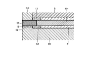
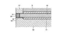
- FIG. 2 is a cross-sectional view showing a cross section taken along line AA in FIG.
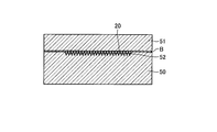
- FIG. 3 is a cross-sectional view showing a cross section taken along line BB in FIG.
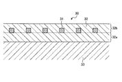
- FIG. 4 is a cross-sectional view showing a cross section taken along the line CC in FIG.
- FIG. 5 is a cross-sectional view taken along the line DD in FIG.
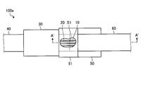
- FIG. 6 is a partially cutaway view showing a configuration of an optical module according to a modification.
- FIG. 7 is a cross-sectional view showing a cross section along line A′-A ′ in FIG. 6.
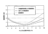
- FIG. 8 is a graph showing the relationship between the relative refractive index difference and the connection loss of the planar lightwave circuit in the first embodiment.
- FIG. 9 is a diagram schematically showing the relationship between the core interval and the positional deviation of the planar lightwave circuit.
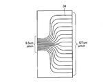
- FIG. 10 is a diagram illustrating the planar lightwave circuit according to the first embodiment.
- FIG. 11 is a flowchart showing a procedure for designing a waveguide using topology optimization.
- FIG. 12 is a diagram illustrating an example of an S-shaped waveguide by a waveguide design using topology optimization.
- FIG. 13 is a partially cutaway view showing the configuration of the optical module according to the second embodiment.
- 14 is a cross-sectional view showing a cross section taken along line B'-B 'in FIG.
- FIG. 15 is a graph showing the relationship between the relative refractive index difference of the planar lightwave circuit and the connection loss in the second embodiment.
- FIG. 1 is a partially cutaway view showing the configuration of the optical module according to the first embodiment, in which the internal configuration of the tape core wire is exposed.
- 2 is a cross-sectional view taken along line AA in FIG. 1
- FIG. 3 is a cross-sectional view taken along line BB in FIG. 1
- FIG. 4 is a cross-sectional view taken along line CC in FIG.
- FIG. 5 is a cross-sectional view taken along the line DD in FIG.
- the optical module 100 includes a single mode optical fiber 10, a high relative refractive index difference optical fiber 20, a planar lightwave circuit 30, a silicon fine wire waveguide 40, and a fixing member 50. ing.
- Single mode optical fiber 10 is, for example, ITU-T G.
- a general silica glass-based optical fiber having a zero dispersion wavelength in the 1.3 ⁇ m band and compliant with 652 can be obtained.
- the relative refractive index difference with respect to the cladding of the core is about 0.3%, and the mode field diameter at 1550 nm is 10 to 11 ⁇ m.
- n c1 is the maximum refractive index of the core
- n c is the refractive index of the cladding.
- This relative refractive index difference is different from that of the high relative refractive index difference optical fiber 20, the planar lightwave circuit 30, and the silicon thin wire waveguide 40. Is similarly defined.
- the high relative refractive index difference optical fiber 20 is an optical fiber having a larger relative refractive index difference of the core relative to the clad than the single mode optical fiber 10.
- the high relative refractive index difference optical fiber 20 is, for example, a silica glass-based optical fiber having a core relative refractive index difference of 2.0% to 3.0%, and a mode field diameter at 1550 nm. Is, for example, 3.0 ⁇ m or more and 5.0 ⁇ m or less.
- the high relative refractive index difference optical fiber 20 has a core diameter of 3 ⁇ m to 4 ⁇ m, for example, and a cutoff wavelength ⁇ c of 1530 nm or less.
- a plurality of single mode optical fibers 10 and high relative refractive index difference optical fibers 20 are arranged in an array, and each single mode optical fiber 10 and high relative refractive index difference optical fiber 20 are fusion spliced at a fusion point S1.
- a plurality of single-mode optical fibers 10 and high relative refractive index difference optical fibers 20 that are fusion-bonded at the fusion point S1 are so-called optical fiber tape cores that are collectively covered in an array. It can be configured as line 60.
- the high relative refractive index difference optical fiber 20 removes the covering of the portion sandwiched between the V-shaped groove 52 provided in the fixing member 50 and the upper plate 51 provided in the fixing member 50. In this state, the fixing member 50 is fixed. Thus, the relative positions of the plurality of high relative refractive index difference optical fibers 20 with respect to the planar lightwave circuit 30 are fixed.
- the fusion point S ⁇ b> 1 between the single mode optical fiber 10 and the high relative refractive index difference optical fiber 20 is not included in the V-shaped groove 52. That is, the region sandwiched between the V-shaped groove 52 and the upper plate 51 is only the high relative refractive index difference optical fiber 20. Therefore, this configuration has an advantage that the fusion point S1 is not subjected to stress from the V-shaped groove 52 and the upper plate 51, and a decrease in reliability of the fusion point S1 due to the stress can be suppressed.
- the fusion point S1 is so-called recoated.
- the coating 11 near the fusion point S1 is peeled off.
- the recoating means that a coating 12 having substantially the same diameter as the coating 11 of the single mode optical fiber 10 is applied to the fusion point S1 after the fusion splicing and the vicinity thereof.
- the gap between the high relative refractive index difference optical fiber 20, the V-shaped groove 52 and the upper plate 51 is filled with the adhesive B. Further, the single mode optical fiber 10 and the high relative refractive index difference optical fiber 20 are fixed to the fixing member 50 as a whole by the adhesive B from above the coatings 11 and 12.
- the planar lightwave circuit 30 includes a clad 32 made of silica glass and a core 31 in which a dopant for increasing the refractive index is added to the silica glass, and the light is confined by the core 31. It is the structure which implement
- the optical waveguide of the planar lightwave circuit 30 is connected to the high relative refractive index difference optical fiber 20 through the connection surface S2.
- the connection surface S ⁇ b> 2 is an end surface on the side not fused-connected to the single mode optical fiber 10.
- the relative refractive index difference between the core 31 and the clad 32 in the planar lightwave circuit 30 is preferably 4% or more and 6% or less for the reason described in detail later.
- Such a relative refractive index difference is realized by adding, for example, zirconia (ZrO 2 ) to the region of the core 31 in the planar lightwave circuit 30.
- the size of the core 31 in the planar lightwave circuit 30 is 2 ⁇ m or more and 4 ⁇ m or less in thickness and 2 ⁇ m or more and 4 ⁇ m or less in width.
- the mode field diameter of such a planar lightwave circuit 30 is, for example, 2 ⁇ m to 4 ⁇ m at a wavelength of 1550 nm.
- the mode field diameter in the planar lightwave circuit 30 and the silicon thin wire waveguide 40 is the diameter of a point that is 5% of the maximum intensity in the NFP (Near-Field Pattern) of the light propagating through the core.
- the mode field is an ellipse, the average value of the major axis and the minor axis is used as the mode field diameter.
- planar lightwave circuit 30 An example of a method for manufacturing the planar lightwave circuit 30 will be briefly described as follows. First, a substrate 33 made of silicon or quartz glass is prepared. Next, a layer made of silica (SiO 2 ) corresponding to the lower clad 32 a that is the clad 32 below the core 31 is formed on the substrate 33 by using a plasma CVD (Chemical Vapor Deposition) method or the like, and then The layer is annealed to become a transparent glass.
- a plasma CVD Chemical Vapor Deposition
- a silica (SiO 2 ) layer doped with zirconia (ZrO 2 ) is formed at a location corresponding to the core 31, and then the layer is annealed to become a transparent glass. Then, a silica (SiO 2 ) layer doped with zirconia (ZrO 2 ) is processed into a desired shape corresponding to the optical waveguide by a photolithography technique, an etching technique, or the like, and the core 31 having a higher refractive index than the clad 32 is formed.
- an upper clad 32b made of silica (SiO 2 ) is formed on the core 31 and the lower clad 32a, and then the layer is annealed to become a transparent glass.
- the silicon fine wire waveguide 40 includes a core 41 made of silicon (Si) and a clad 42 having a refractive index lower than that of the core 41, and the light is confined and guided by the core 41. It is the structure which implement
- the silicon fine wire waveguide 40 is a silicon fine wire waveguide element or chip including an optical waveguide having a core 41 made of silicon (Si) and a clad 42 having a refractive index lower than that of the core 41.
- the silicon thin wire waveguide 40 may be an optical switch, a light emitting element, or the like integrated on the same substrate.
- connection surface S3 is an end surface on the side not connected to the high relative refractive index difference optical fiber 20.
- the relative refractive index difference between the core 41 and the clad 42 in the silicon fine wire waveguide 40 is, for example, about 40%. Moreover, the size and width of the core 41 in the silicon fine wire waveguide 40 are, for example, several hundred nm.
- the silicon thin wire waveguide 40 is manufactured using, for example, a CMOS process.
- the CMOS process refers to the same manufacturing process as a standard process for manufacturing a CMOS on a silicon substrate.
- the configuration example of the silicon fine wire waveguide 40 is a configuration in which the core 41 is embedded in the clad 42, but it may be a waveguide other than the embedded type such as a ridge type waveguide.
- the material of the clad 42 is not limited to silica (SiO 2 ), and other materials can be used, or a part of the clad 42 can be air.
- the relative refractive index difference of the core with respect to the clad in the single mode optical fiber 10 is ⁇ 1
- the high relative refractive index difference optical fiber 20 is summarized
- the relative refractive index difference of the core with respect to the clad is ⁇ 2
- the relative refractive index difference of the core with respect to the clad in the planar lightwave circuit 30 is ⁇ 3
- the relative refractive index difference of the core with respect to the clad in the silicon wire waveguide 40 is ⁇ 4
- ⁇ 1 is , About 0.3%
- ⁇ 2 is 2.0% or more and 3.0% or less
- ⁇ 3 is 4% or more and 6% or less
- ⁇ 4 is about 40%. Therefore, in the relationship of the relative refractive index difference of each component in the optical module 100, ⁇ 1 ⁇ 2 ⁇ 3 ⁇ 4 The relationship is satisfied.
- FIG. 6 is a partially cutaway view showing the configuration of the optical module according to the modification, in which the configuration inside the tape core wire is exposed.
- FIG. 7 is a cross-sectional view showing a cross section along line A′-A ′ in FIG. Since the optical module 100a according to the modified example has many common configurations with the optical module 100 according to the first embodiment, only different configurations will be described here.
- the optical module 100a according to the modified example is similar to the optical module 100 according to the first embodiment.
- a thin wire waveguide 40 and a fixing member 50 are provided.
- a plurality of single mode optical fibers 10 and high relative refractive index difference optical fibers 20 are arranged in an array, and each single mode optical fiber 10 and high relative refractive index difference optical fiber 20 are fused. It is fusion spliced at S1.
- a plurality of single-mode optical fibers 10 and high relative refractive index difference optical fibers 20 that are fusion-bonded at the fusion point S1 are so-called optical fiber tape cores that are collectively covered in an array. It can be configured as line 60.
- the optical module 100a according to the modification is sandwiched between the V-shaped groove 52 provided in the fixing member 50 and the upper plate 51 provided in the fixing member 50. Therefore, unlike the optical module 100 according to the first embodiment, the optical module 100a according to the modification is not recoated at the fusion point S1. That is, in the optical module 100a according to the modification, the upper plate 51 provided in the fixing member 50 and the V-shaped groove 52 provided in the fixing member 50 in a part of the high relative refractive index difference optical fiber 20 and the single mode optical fiber 10. It is fixed to the fixing member 50 in a state where the covering of the portion sandwiched between the two is removed.
- the fiber diameter in the vicinity of the fusion point S1 is reduced so that the reliability of the fusion point S1 does not decrease due to the stress between the V-shaped groove 52 and the upper plate 51. It is preferable to perform such processing.
- the manufacture since it is not necessary to perform recoating, the manufacture becomes easy.
- optical module 100a according to the modified example as described above has the same effect as the optical module 100 according to the first embodiment.
- the configuration of the optical module 100 according to the first embodiment can reduce the connection loss between the single mode optical fiber 10 and the silicon wire waveguide 40 with a simple configuration.
- the operation principle leading to the effect will be described.
- FIG. 8 is a graph showing the relationship between the relative refractive index difference ⁇ of the planar lightwave circuit (PLC) and the connection loss in the first embodiment.
- the connection loss between the single mode optical fiber (SMF) and the planar lightwave circuit one-dot chain line
- the connection loss between the silicon (Si) thin wire waveguide and the planar lightwave circuit solid line
- the total connection loss broken line
- the connection loss shown in FIG. 8 is the connection loss in the outermost channel when the optical module 100 has 40 channels, that is, when there are 40 optical waveguides from the single mode optical fiber to the silicon fine wire waveguide. is there.
- connection loss can be reduced to near the limit by selecting a high relative refractive index difference optical fiber that matches the mode field diameter of the planar lightwave circuit.
- the mode field diameter of the high relative refractive index difference optical fiber at this time is about 3 ⁇ m, and the relative refractive index difference of the planar lightwave circuit capable of realizing this mode field diameter is 5%.
- the relative refractive index difference of the planar lightwave circuit is larger than 5%, a high relative refractive index difference optical fiber that matches the mode field diameter of the planar lightwave circuit cannot be selected, and the connection loss increases. .
- connection loss between the single-mode optical fiber and the planar lightwave circuit is very low when the relative refractive index difference of the planar lightwave circuit is 5% or less, as shown by the dashed line in FIG.
- the connection loss tends to increase gradually.
- the relative refractive index difference of the planar lightwave circuit when the relative refractive index difference of the planar lightwave circuit is larger, it is possible to suppress the connection loss due to the positional deviation between the silicon thin wire waveguide and the planar lightwave circuit.
- the reason is that when the relative refractive index difference of the planar lightwave circuit is small, it is necessary to increase the core interval of the planar lightwave circuit, and the influence of the warp generated in the planar lightwave circuit becomes large.
- the planar lightwave circuit since quartz glass is deposited on a silicon substrate, warpage occurs due to a difference in linear expansion coefficient between silicon and quartz glass. For this reason, the one where the relative refractive index difference of the planar lightwave circuit is larger is more advantageous from the viewpoint of suppressing the connection loss.
- FIG. 9 is a diagram schematically showing the relationship between the core interval and the positional deviation of the planar lightwave circuit.
- FIG. 9 shows a comparison between (a) the case where the core interval of the planar lightwave circuit is narrow and (b) the case where the core interval of the planar lightwave circuit is wide.
- (a) and (b) have shown the position in the cross-sectional direction of the core in case the same amount of curvature has generate
- the vertical deviation between the center core 31c1 and the end core 31e1 is h1
- the core interval P2 of the planar lightwave circuit is wide.
- the vertical shift between the center core 31c2 and the end core 31e2 is h2. That is, the smaller the core interval of the planar lightwave circuit is, the smaller the deviation between the cores at the center and at the end is suppressed.
- the relative refractive index difference is 1.5%
- the core interval can be set narrow as 8 ⁇ m.
- the relative refractive index difference of the planar lightwave circuit is small. It is preferable that the relative refractive index difference of the lightwave circuit is large. From these two effects, the minimum value of the connection loss appears in the vicinity of the relative refractive index difference of the planar lightwave circuit being 5% as shown in the graph of FIG.
- the graph (broken line) of the total connection loss from the single mode optical fiber to the silicon wire waveguide shown in FIG. 8 shows the connection loss between the single mode optical fiber and the planar lightwave circuit described above, the silicon wire waveguide,
- the connection loss is the sum of the connection loss with the planar lightwave circuit.
- the total connection loss from the single-mode optical fiber to the silicon wire waveguide is minimized when the relative refractive index difference of the planar lightwave circuit is around 5%.
- the relative refractive index difference of the planar lightwave circuit is 4% or more and 6% or less.
- the relative refractive index difference of the planar lightwave circuit is preferably 4% or more and 6% or less from the viewpoint of reducing the overall size of the optical module.
- the minimum bending radius of the optical waveguide that can be formed in the planar lightwave circuit is about 100 times the minimum bending radius of the silicon wire waveguide. End up.
- the size of the entire optical module is substantially limited to the size of the planar lightwave circuit, and the merit of the silicon wire waveguide that is small is reduced. Therefore, in order to enjoy the merit of the silicon thin wire waveguide and reduce the size of the entire optical module, it is preferable that the relative refractive index difference of the planar lightwave circuit is 4% or more and 6% or less.
- the silicon fine wire waveguide 40 has a lower clad 42a laminated on a substrate 43, and a core 41 formed thereon.
- the thickness of the lower clad 42a is generally 2 to 3 ⁇ m. Therefore, if the mode field diameter in the silicon fine wire waveguide 40 is made larger than 3 ⁇ m to some extent, absorption of propagation light (mode absorption) by the substrate 43 occurs.
- the mode field diameter of the planar lightwave circuit is preferably about 3 ⁇ m, and the relative refractive index difference for realizing the mode field diameter is preferably 4% or more and 6% or less.
- Example 1 Here, examples of the optical module according to the first embodiment described above will be described.
- the optical module according to Example 1 is configured in the same manner as in FIG. 1 except that a planar lightwave circuit, a high relative refractive index difference optical fiber, and a single mode optical fiber are sequentially connected to both ends of the silicon fine wire waveguide. This is an experimental configuration in which light input from one single mode optical fiber is output from the other single mode optical fiber.
- the planar lightwave circuit according to the first embodiment is a planar lightwave circuit having a function of 16-core pitch conversion, and has a configuration in which S-shaped waveguides 34 are arranged in parallel as shown in FIG.
- the minimum value of the bending radius in the S-shaped waveguide 34 is 400 ⁇ m
- the core interval at the end face connected to the high relative refractive index difference optical fiber is 127 ⁇ m
- the core interval at the end face connected to the silicon fine wire waveguide is 8 ⁇ m. .5 ⁇ m.
- the size of the core in the planar lightwave circuit is 3 ⁇ m ⁇ 3 ⁇ m, and the core material is made by doping silica (SiO 2 ) with zirconia (ZrO 2 ). At this time, the relative refractive index difference between the core and the clad of the planar lightwave circuit is 5%, and the mode field diameter is 3 ⁇ m.
- the mode field diameter of the silicon wire waveguide according to Example 1 is set to 3 ⁇ m to match the mode field diameter of the planar lightwave circuit.
- the mode field diameter of the high relative refractive index difference optical fiber according to the first embodiment is also set to 3 ⁇ m to match the mode field diameter of the planar lightwave circuit.
- the high relative refractive index difference optical fiber is fusion-spliced with the single mode optical fiber, and the connection loss for this connection is about 0.05 dB.
- connection loss between the planar lightwave circuit and the single mode optical fiber is 0.3 to 0.5 dB, and the connection loss in the entire optical module is 0. 9 to 1.3 dB. Therefore, in the optical module according to Example 1, the connection loss between the silicon fine wire waveguide and the single mode optical fiber is reduced with a simple configuration.
- the optical module according to the second embodiment is a configuration example in which the planar lightwave circuit is downsized as compared with the optical module according to the first embodiment.
- miniaturization of the planar lightwave circuit is achieved by a method of reducing the minimum bending radius in the S-shaped waveguide 34 shown in FIG. 10 from 400 ⁇ m to 100 ⁇ m by using the waveguide design using topology optimization.
- Waveguide design using topology optimization is to realize the desired loss by calculating the loss of the optical waveguide while changing the refractive index distribution of the optical waveguide given as the initial value and repeating the minute change. This is one of the design methods for specifying the shape of the optical waveguide.
- FIG. 11 is a flowchart showing a procedure for designing a waveguide using topology optimization.
- an input-side optical field and an output-side optical field are set in the waveguide to be designed (step S11).
- data is set such that an optical field having a mode field diameter of 3 ⁇ m is input from a high relative refractive index difference optical fiber, and an optical field having a mode field diameter of 3 ⁇ m is output to a silicon wire waveguide.
- an initial value of the optical waveguide shape for starting topology optimization is set (step S12).
- the minimum value of the bending radius is 100 ⁇ m
- the core interval at the end face connected to the high relative refractive index difference optical fiber is 127 ⁇ m
- the core interval at the end face connected to the silicon thin wire waveguide is 8.
- a rough optical waveguide that realizes an S-shaped waveguide of 5 ⁇ m may be set as an initial value.
- step S13 an optical waveguide analysis is performed by a finite element method, and a change in the optical field when the waveguide structure (refractive index distribution) is minutely changed is calculated by the sensitivity analysis (step S13). Then, the waveguide structure is changed in a direction in which characteristics are improved, which is determined in step S13 (step S14).
- step S15 it is determined whether the output light field satisfies the specified value (step S15), and the shape of the optical waveguide that realizes the desired characteristics is specified.
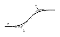
- FIG. 12 is a diagram showing an example of the S-shaped waveguide by the waveguide design using the topology optimization described above.
- a plurality of hook-shaped auxiliary waveguides 35 are formed along the S-shaped waveguide 34 in the region along the outer periphery of the S-shaped waveguide 34 according to the second embodiment.
- These saddle-shaped auxiliary waveguides 35 are responsible for returning the energy of light leaking from the S-shaped waveguide 34 when propagating through the S-shaped waveguide 34 to the S-shaped waveguide 34 as a result. Contributes to suppressing the bending loss of light propagating through the S-shaped waveguide 34.
- an S-shaped waveguide in which a plurality of hook-shaped auxiliary waveguides are formed along the bending waveguide in a region along the outer periphery of the bending waveguide By using it, in the planar lightwave circuit according to the first embodiment, the bending radius of 400 ⁇ m can be reduced to 100 ⁇ m. As a result, almost no increase in bending loss is observed. In the planar lightwave circuit according to the second embodiment, the size of 2 mm ⁇ 3.5 mm in the planar lightwave circuit according to the first embodiment is reduced to 1.5 mm ⁇ 3.5 mm. That is, the area ratio of the planar lightwave circuit can be reduced by 3/4.
- the waveguide design using topology optimization is used.
- the planar lightwave circuit according to the second embodiment may be designed by the wavefront matching method or other optimization designs.
- the auxiliary waveguide is simply formed in the region along the outer periphery of the bending waveguide along the bending waveguide. The waveguide has an effect of suppressing bending loss of light propagating through the bending waveguide.
- an auxiliary waveguide for suppressing bending loss is provided for the pitch-converting S-shaped waveguide.
- the present invention is not limited to this configuration. It is possible to provide an auxiliary waveguide for suppressing bending loss with respect to the bending waveguide formed in general.
- the first embodiment has a configuration of a multi-fiber connection optical module, but the embodiment of the present invention is not limited to this, and can be applied to a single-core connection optical module.
- the configuration of the optical module according to the second embodiment having a single-core connection and the characteristics of the connection loss will be described.
- the description of the substantially common configuration is omitted.
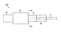
- FIG. 13 is a partially cutaway view showing the configuration of the optical module according to the second embodiment
- FIG. 14 is a cross-sectional view showing a cross section taken along line B′-B ′ in FIG. 13.
- the optical module 200 according to the second embodiment is similar to the optical module 100 according to the first embodiment in that a single mode optical fiber, a high relative refractive index difference optical fiber, a planar lightwave circuit 30, and silicon are used.
- a thin wire waveguide 40 and a fixing member 50 are provided.
- an optical fiber core 61 coated with a single-mode optical fiber and a high relative refractive index difference optical fiber being fused and connected is illustrated. Contains a single mode optical fiber and a high relative refractive index difference optical fiber.
- the high relative refractive index difference optical fiber 20 includes the V-shaped groove 52 provided in the fixing member 50 and the same as in the first embodiment. It is being fixed to the fixing member 50 in the state from which the coating
- FIG. 15 is a graph showing the relationship between the relative refractive index difference ⁇ of the planar lightwave circuit (PLC) and the connection loss in the second embodiment.
- the graph shown in FIG. 15 shows the connection loss between the single mode optical fiber (SMF) and the planar lightwave circuit (one-dot chain line), and the connection loss between the silicon (Si) thin wire waveguide and the planar lightwave circuit (solid line). ) And the total connection loss (broken line) from the single mode optical fiber to the silicon wire waveguide.
- SMF single mode optical fiber
- Si silicon
- solid line planar lightwave circuit
- the connection loss between the single mode optical fiber and the planar lightwave circuit is 5 relative refractive index differences of the planar lightwave circuit.
- the ratio is less than or equal to%, a very low state can be maintained.
- the relative refractive index difference of the planar lightwave circuit becomes larger than 5%, the connection loss tends to gradually increase accordingly.
- the high relative refractive index difference optical fiber can suppress the relative refractive index difference to 3% or less in order to manufacture stably. preferable.
- the relative refractive index difference of the planar lightwave circuit is larger than 5%, a high relative refractive index difference optical fiber that matches the mode field diameter of the planar lightwave circuit cannot be selected, and the connection loss increases. .
- connection loss between the silicon thin wire waveguide and the planar lightwave circuit is the relative refractive index difference of the planar lightwave circuit.
- the minimum connection loss appears in the vicinity of 5%.
- the mode field diameter of the silicon fine wire waveguide is preferably 3 ⁇ m or less.
- the mode field diameter in the silicon fine wire waveguide 40 is larger than 3 ⁇ m, the propagation of the propagation light (mode absorption) by the substrate 43 occurs. Therefore, when the mode field diameter in the silicon fine wire waveguide 40 is enlarged, it becomes necessary to perform a separate manufacturing process such as hollowing out the substrate 43 below the core 41 after the CMOS process, which complicates the manufacturing process. Will be invited. Therefore, in order to form the silicon fine wire waveguide only by the CMOS process, the mode field diameter of the silicon fine wire waveguide 40 is preferably set to 3 ⁇ m or less. In order to suppress the connection loss with the silicon fine wire waveguide 40 having a mode field diameter of 3 ⁇ m or less, the relative refractive index difference of the planar lightwave circuit 30 is preferably 5% or more.
- the minimum value of the connection loss appears when the relative refractive index difference of the planar lightwave circuit is around 5%.
- the total connection loss graph (broken line) from the single mode optical fiber to the silicon wire waveguide shown in FIG. 15 is a combination of the above two connection losses, and the relative refractive index difference of the planar lightwave circuit is 5%.
- the minimum value of splice loss appears in the vicinity of. Therefore, also in the optical module 200 according to the second embodiment, it is preferable that the relative refractive index difference of the planar lightwave circuit 30 is 4% or more and 6% or less, as in the first embodiment.
- a spot size converter for converting the spot size of the guided light is provided on the end face for the high relative refractive index difference optical fiber or the end face for the silicon fine wire waveguide in the planar lightwave circuit.
- a spot size converter may be provided on the end surface of the silicon thin wire waveguide with respect to the planar lightwave circuit, thereby further improving the mode field diameter matching. It goes without saying that the connection loss between the silicon wire waveguide and the single-mode optical fiber is further reduced if the matching of the mode field diameter is further improved by these devices.
- the optical module according to the present invention is useful for connecting a silicon fine wire waveguide and a single mode optical fiber.
- Optical module 10 Single mode optical fiber 11, 12 Coating 20 High relative refractive index difference optical fiber 30 Planar lightwave circuit 31, 31c1, 31c2, 31e1, 31e2, 41 Core 32, 42 Clad 32a, 42a Lower clad 32b , 42b Upper clad 33, 43 Substrate 34 S-shaped waveguide 35 Auxiliary waveguide 40 Silicon wire waveguide 50 Fixed member 51 Upper plate 52 V-shaped groove 60 Optical fiber ribbon 61 Optical fiber ribbon
Landscapes
- Physics & Mathematics (AREA)
- General Physics & Mathematics (AREA)
- Optics & Photonics (AREA)
- Engineering & Computer Science (AREA)
- Plasma & Fusion (AREA)
- Microelectronics & Electronic Packaging (AREA)
- Optical Integrated Circuits (AREA)
- Optical Couplings Of Light Guides (AREA)
Abstract
シングルモード光ファイバと、シングルモード光ファイバよりも、クラッドに対するコアの比屈折率差が大きく、シングルモード光ファイバと融着接続された高比屈折率差光ファイバと、石英系ガラスからなるクラッドと石英系ガラスに屈折率を高めるドーパントを添加したコアとを有し、コアによって光を導波する光導波路がシングルモード光ファイバと融着接続されていない側の高比屈折率差光ファイバの端面に接続された平面光波回路と、シリコンからなるコアとコアよりも屈折率が低いクラッドとを有し、コアによって光を導波するシリコン細線導波路が高比屈折率差光ファイバと接続されていない側の平面光波回路の端面における光導波路に接続されたシリコン細線導波路素子と、を備えることを特徴とする光学モジュール。
Description
本発明は、光学モジュールに関する。
シリコン細線導波路は、比屈折率差Δが例えば40%を超えることがあり、それゆえに、モードフィールド径も極めて小さい。したがって、シリコン細線導波路を通常のシングルモード光ファイバと直接接続した場合、モードフィールド径の違いから、5dB程度の大きな接続損失が生じてしまう。このモードフィールド径の違いに起因する接続損失の低減は、シリコン細線導波路を実用化する上で解決すべき技術課題の一つである。
そこで、この接続損失を低減するために、例えば、シリコン細線導波路の端部にモードフィールド径を調節するための特殊な構造を設ける試みが検討されている(非特許文献1および2参照)。
T. Barwicz, et al., "An O-band Metamaterial Converter Interfacing Standard Optical Fibers to Silicon Nanophotonic Waveguides," in Optical Fiber Communication Conference 2015, paper Th3F.3.
S. Nakamura, et al., "Compact and Low-Loss 8x8 Silicon Photonic Switch Module for Transponder Aggregators in CDC-ROADM Application," in Optical Fiber Communication Conference 2015 paper M2B.6.
非特許文献1または非特許文献2のように、シリコン細線導波路の端部に特殊な構造を設けることでも、原理的には接続損失を低減することができるが、シリコン細線導波路の製造プロセスが煩雑化され、歩留まりの悪化やコスト増加を引き起こすという問題がある。また、シリコン細線導波路とシングルモード光ファイバとを多心接続しようとする場合、ポート間の均一性が大幅に劣化してしまう場合がある。
本発明は、上記に鑑みてなされたものであって、その目的は、シリコン細線導波路とシングルモード光ファイバとの間の接続損失を簡便な構成で低減する光学モジュールを提供することにある。
上述した課題を解決し、目的を達成するために、本発明の一態様に係る光学モジュールは、シングルモード光ファイバと、前記シングルモード光ファイバよりも、クラッドに対するコアの比屈折率差が大きく、前記シングルモード光ファイバと融着接続された高比屈折率差光ファイバと、石英系ガラスからなるクラッドと前記石英系ガラスに屈折率を高めるドーパントを添加したコアとを有し、前記コアによって光を導波する光導波路が前記シングルモード光ファイバと融着接続されていない側の前記高比屈折率差光ファイバの端面に接続された平面光波回路と、シリコンからなるコアと前記コアよりも屈折率が低いクラッドとを有し、前記コアによって光を導波するシリコン細線導波路が前記高比屈折率差光ファイバと接続されていない側の平面光波回路の端面における光導波路に接続されたシリコン細線導波路素子と、を備えることを特徴とする。
また、本発明の一態様に係る光学モジュールは、前記シングルモード光ファイバにおけるクラッドに対するコアの比屈折率差をΔ1とし、前記高比屈折率差光ファイバにおけるクラッドに対するコアの比屈折率差をΔ2とし、前記平面光波回路におけるクラッドに対するコアの比屈折率差をΔ3とし、前記シリコン細線導波路におけるクラッドに対するコアの比屈折率差をΔ4とすると、
Δ1<Δ2<Δ3<Δ4
という関係を満たすことを特徴とする。
Δ1<Δ2<Δ3<Δ4
という関係を満たすことを特徴とする。
また、本発明の一態様に係る光学モジュールは、前記平面光波回路の比屈折率差であるΔ3は、4%≦Δ3≦6%であることを特徴とする。
また、本発明の一態様に係る光学モジュールは、前記平面光波回路のコアに添加したドーパントは、ジルコニアであることを特徴とする。
また、本発明の一態様に係る光学モジュールは、前記平面光波回路に形成された光導波路のうち、曲げ導波路の外周に沿った領域には、前記曲げ導波路を伝搬する光の曲げ損失を抑制する補助導波路が形成されていることを特徴とする。
また、本発明の一態様に係る光学モジュールは、前記平面光波回路に形成された光導波路は、初期値として与えられた光導波路形状を微小変化させ、当該微小変化を繰り返しながら光導波路の損失を計算することにより、所望の損失を実現するものとして特定された形状であることを特徴とする。
また、本発明の一態様に係る光学モジュールは、前記シングルモード光ファイバおよび前記高比屈折率差光ファイバは、複数本がアレイ状に配列された状態で前記平面光波回路の対応する光導波路に接続されていることを特徴とする。
また、本発明の一態様に係る光学モジュールは、前記平面光波回路に対する前記複数本の高比屈折率差光ファイバの相対的位置を固定するための固定部材をさらに備え、前記高比屈折率差光ファイバは、前記固定部材に設けられたV字溝と前記固定部材が備える上板とに挟持される部分の被覆が除去された状態で、前記固定部材に固定される、ことを特徴とする。
また、本発明の一態様に係る光学モジュールは、前記平面光波回路は、前記高比屈折率差光ファイバに接続される端面におけるコア間の間隔よりも、前記シリコン細線導波路素子に接続される端面におけるコア間の間隔の方が狭くなるように複数のS字導波路が配列された構成であることを特徴とする。
また、本発明の一態様に係る光学モジュールは、前記平面光波回路または前記シリコン細線導波路素子は、導波する光のスポットサイズを変換するためのスポットサイズコンバータを備えることを特徴とする。
本発明に係る光学モジュールは、シリコン細線導波路とシングルモード光ファイバとの間の接続損失を簡便な構成で低減することができるという効果を奏する。
以下、本発明に係る光学部品の実施形態について、図面を参照しながら説明する。なお、以下に説明する実施形態により本発明が限定されるものではない。また、各図面において、同一または対応する要素には適宜同一の符号を付している。さらに、図面は模式的なものであり、各要素の寸法の関係や比率などは、現実のものとは異なる場合があることに留意する必要がある。図面の相互間においても、互いの寸法の関係や比率が異なる部分が含まれている場合がある。また、本明細書で特に定義しない用語についてはITU-T G.650.1における定義、測定方法に適宜従うものとする。
(第1実施形態)
図1は、第1実施形態に係る光学モジュールの構成を示す一部破断図であり、テープ心線の内部の構成を露出させて記載している。図2は、図1におけるA-A線断面を示す断面図であり、図3は、図1におけるB-B線断面を示す断面図であり、図4は、図1におけるC-C線断面を示す断面図であり、図5は、図1におけるD-D線断面を示す断面図である。
図1は、第1実施形態に係る光学モジュールの構成を示す一部破断図であり、テープ心線の内部の構成を露出させて記載している。図2は、図1におけるA-A線断面を示す断面図であり、図3は、図1におけるB-B線断面を示す断面図であり、図4は、図1におけるC-C線断面を示す断面図であり、図5は、図1におけるD-D線断面を示す断面図である。
図1に示すように、第1実施形態に係る光学モジュール100は、シングルモード光ファイバ10と高比屈折率差光ファイバ20と平面光波回路30とシリコン細線導波路40と固定部材50とを備えている。
シングルモード光ファイバ10は、例えばITU-T G.652に準拠する、1.3μm帯にゼロ分散波長を持つ一般的な石英ガラス系の光ファイバとすることができる。シングルモード光ファイバ10において、コアのクラッドに対する比屈折率差は約0.3%であり、1550nmにおけるモードフィールド径は10~11μmである。
ここで、比屈折率差とは、以下で定まる数値である。
Δ={(nc1-nc)/nc1}×100
ただし、nc1はコアの最大屈折率、ncはクラッドの屈折率であり、この比屈折率差は、高比屈折率差光ファイバ20と平面光波回路30とシリコン細線導波路40に対しても同様に定義される。
Δ={(nc1-nc)/nc1}×100
ただし、nc1はコアの最大屈折率、ncはクラッドの屈折率であり、この比屈折率差は、高比屈折率差光ファイバ20と平面光波回路30とシリコン細線導波路40に対しても同様に定義される。
高比屈折率差光ファイバ20は、シングルモード光ファイバ10よりもクラッドに対するコアの比屈折率差が大きい光ファイバである。具体的には、高比屈折率差光ファイバ20は、例えばクラッドに対するコアの比屈折率差が2.0%以上3.0%以下の石英ガラス系の光ファイバであり、1550nmにおけるモードフィールド径は例えば3.0μm以上5.0μm以下である。また、高比屈折率差光ファイバ20は、たとえばコア径が3μm~4μmであり、カットオフ波長λcが、1530nm以下である。
シングルモード光ファイバ10および高比屈折率差光ファイバ20は、複数本がアレイ状に配列され、各シングルモード光ファイバ10と高比屈折率差光ファイバ20とが融着点S1で融着接続されている。融着点S1で融着接続された複数本のシングルモード光ファイバ10および高比屈折率差光ファイバ20は、アレイ状に配列された状態で一括して被覆されている、いわゆる光ファイバテープ心線60として構成することが可能である。
図2および図3に示すように、高比屈折率差光ファイバ20は、固定部材50に設けられたV字溝52と固定部材50が備える上板51とに挟持される部分の被覆が除去された状態で固定部材50に固定されている。これにより、平面光波回路30に対する複数本の高比屈折率差光ファイバ20の相対的位置を固定している。
図2および図3に示されるように、シングルモード光ファイバ10と高比屈折率差光ファイバ20の融着点S1は、V字溝52の内部に含まれない位置となっている。すなわち、V字溝52と上板51との間で挟持される領域は、高比屈折率差光ファイバ20のみとなる。したがって、本構成は、融着点S1がV字溝52および上板51から応力を受けることがなく、応力による融着点S1の信頼性の低下を抑制できるというメリットがある。
図2に示されるように、融着点S1は、いわゆるリコートが施されている。シングルモード光ファイバ10と高比屈折率差光ファイバ20とを融着接続する際には、融着点S1の近傍の被覆11を剥ぐことになる。リコートとは、融着接続後の融着点S1およびその近傍に、シングルモード光ファイバ10の被覆11と略同径の被覆12を施すことである。
また、高比屈折率差光ファイバ20とV字溝52および上板51との隙間は、接着剤Bによって充填されている。さらに、シングルモード光ファイバ10および高比屈折率差光ファイバ20は、被覆11,12の上から、接着剤Bで固定部材50に全体的に固定されている。
図1および図4に示すように、平面光波回路30は、石英系ガラスからなるクラッド32と石英系ガラスに屈折率を高めるドーパントを添加したコア31とを有し、コア31によって光を閉じ込めて導波する光導波路を実現する構成である。平面光波回路30の光導波路は、高比屈折率差光ファイバ20と接続面S2で接続されている。ここで、高比屈折率差光ファイバ20にとって接続面S2は、シングルモード光ファイバ10と融着接続されていない側の端面である。
平面光波回路30におけるコア31とクラッド32と比屈折率差は、後に詳述する理由により、4%以上6%以下とすることが好ましい。このような比屈折率差は、平面光波回路30におけるコア31の領域に、例えばジルコニア(ZrO2)を添加することによって実現される。また、平面光波回路30におけるコア31の大きさは、厚さが2μm以上4μm以下であり、幅が2μm以上4μm以下である。このような平面光波回路30のモードフィールド径は、例えば波長1550nmにおいて、2μm~4μmとなる。
なお、平面光波回路30、およびシリコン細線導波路40におけるモードフィールド径は、コアを伝搬する光のNFP(Near-Field Pattern)において、最大強度の5%の強度となる点の直径とする。なお、モードフィールドが楕円の場合は長径と短径の平均値をモードフィールド径とする。
平面光波回路30の製造方法の例を簡略的に示せば以下の通りである。最初に、シリコンや石英ガラスなどで形成された基板33を用意する。次に、コア31よりも下のクラッド32である下部クラッド32aに対応するシリカ(SiO2)からなる層をプラズマCVD(Chemical Vapor Deposition)法などを用いて基板33上に形成し、その後、当該層をアニールして透明ガラス化する。
次に、スパッタ法を用いて、コア31に対応する箇所にジルコニア(ZrO2)がドープされたシリカ(SiO2)層を形成し、その後、当該層をアニールして透明ガラス化する。そして、フォトリソグラフィ技術やエッチング技術等によって、光導波路に対応する所望の形状にジルコニア(ZrO2)がドープされたシリカ(SiO2)層を加工し、クラッド32よりも屈折率の高いコア31を形成する。
その後、コア31および下部クラッド32aの上に、シリカ(SiO2)からなる上部クラッド32bを形成し、その後、当該層をアニールして透明ガラス化する。
図1および図5に示すように、シリコン細線導波路40は、シリコン(Si)からなるコア41とコア41よりも屈折率が低いクラッド42とを有し、コア41により光を閉じ込めて導波する光導波路を実現する構成である。なお、ここでのシリコン細線導波路40は、シリコン(Si)からなるコア41とコア41よりも屈折率が低いクラッド42とを有する光導波路を含むシリコン細線導波路素子ないしチップ等を示している。例えば、シリコン細線導波路40は、光スイッチや発光素子等が同一基板上に集積されたものとし得る。
シリコン細線導波路40の光導波路は、平面光波回路30の光導波路と接続面S3で接続されている。ここで、平面光波回路30にとって接続面S3は、高比屈折率差光ファイバ20と接続されていない側の端面である。
シリコン細線導波路40におけるコア41とクラッド42との比屈折率差は、例えば約40%である。また、シリコン細線導波路40におけるコア41の大きさと幅は、例えば数百nmである。
シリコン細線導波路40は、たとえばCMOSプロセスを用いて製造される。ここで、CMOSプロセスとは、シリコン基板上にCMOSを製造するための標準的プロセスと同一の製造プロセスのことをいう。
なお、上記シリコン細線導波路40の構成例は、コア41がクラッド42に埋め込まれた構成であるが、リッジ型の導波路等、埋め込み型以外の導波路であってもよい。また、クラッド42の材料も、シリカ(SiO2)に限らず、他の材料を用いることや、クラッド42の一部を空気とすることも可能である。
ここで、上記構成の光学モジュール100における各構成の比屈折率差の関係についてまとめると、シングルモード光ファイバ10におけるクラッドに対するコアの比屈折率差をΔ1とし、高比屈折率差光ファイバ20におけるクラッドに対するコアの比屈折率差をΔ2とし、平面光波回路30におけるクラッドに対するコアの比屈折率差をΔ3とし、シリコン細線導波路40におけるクラッドに対するコアの比屈折率差をΔ4とすると、Δ1は、約0.3%であり、Δ2は、2.0%以上3.0%以下であり、Δ3は、4%以上6%以下であり、Δ4は、約40%である。したがって、光学モジュール100における各構成の比屈折率差の関係において、
Δ1<Δ2<Δ3<Δ4
という関係が満たされている。
Δ1<Δ2<Δ3<Δ4
という関係が満たされている。
(変形例)
ここで、図6および図7を参照しながら、第1実施形態に係る光学モジュール100の変形例について説明する。図6は、変形例に係る光学モジュールの構成を示す一部破断図であり、テープ心線の内部の構成を露出させて記載している。図7は、図6におけるA’-A’線断面を示す断面図である。なお、変形例に係る光学モジュール100aは、第1実施形態に係る光学モジュール100と共通の構成が多いので、ここでは相違する構成のみ説明する。
ここで、図6および図7を参照しながら、第1実施形態に係る光学モジュール100の変形例について説明する。図6は、変形例に係る光学モジュールの構成を示す一部破断図であり、テープ心線の内部の構成を露出させて記載している。図7は、図6におけるA’-A’線断面を示す断面図である。なお、変形例に係る光学モジュール100aは、第1実施形態に係る光学モジュール100と共通の構成が多いので、ここでは相違する構成のみ説明する。
図6に示すように、変形例に係る光学モジュール100aは、第1実施形態に係る光学モジュール100と同様に、シングルモード光ファイバ10と高比屈折率差光ファイバ20と平面光波回路30とシリコン細線導波路40と固定部材50とを備えている。
また、同様に、シングルモード光ファイバ10および高比屈折率差光ファイバ20は、複数本がアレイ状に配列され、各シングルモード光ファイバ10と高比屈折率差光ファイバ20とが融着点S1で融着接続されている。融着点S1で融着接続された複数本のシングルモード光ファイバ10および高比屈折率差光ファイバ20は、アレイ状に配列された状態で一括して被覆されている、いわゆる光ファイバテープ心線60として構成することが可能である。
一方、図7に示すように、変形例に係る光学モジュール100aでは、融着点S1が固定部材50に設けられたV字溝52と固定部材50が備える上板51とに挟持されている。したがって、変形例に係る光学モジュール100aは、第1実施形態に係る光学モジュール100とは異なり、融着点S1にリコートが施されていない。すなわち、変形例に係る光学モジュール100aでは、高比屈折率差光ファイバ20とシングルモード光ファイバ10の一部において、固定部材50に設けられたV字溝52と固定部材50が備える上板51とに挟持される部分の被覆が除去された状態で、固定部材50に固定されることになる。
したがって、変形例に係る光学モジュール100aでは、融着点S1がV字溝52と上板51との間の応力によって信頼性が低下しないように、融着点S1の近傍のファイバ径を細くする等の加工をすることが好ましい。一方で、変形例に係る光学モジュール100aでは、リコートを施す必要がないので、製造が容易になる。
上記のような変形例に係る光学モジュール100aも、第1実施形態に係る光学モジュール100と同様の効果を奏する構成である。
(作用原理)
ここで、図8を参照しながら、第1実施形態に係る光学モジュール100の構成が、シングルモード光ファイバ10とシリコン細線導波路40との間の接続損失を簡便な構成で低減することができるという効果を導く作用原理について説明する。
ここで、図8を参照しながら、第1実施形態に係る光学モジュール100の構成が、シングルモード光ファイバ10とシリコン細線導波路40との間の接続損失を簡便な構成で低減することができるという効果を導く作用原理について説明する。
図8は、第1実施形態における、平面光波回路(PLC)の比屈折率差Δと接続損失との関係を示すグラフである。図8に示されるグラフには、シングルモード光ファイバ(SMF)と平面光波回路との間の接続損失(一点鎖線)、シリコン(Si)細線導波路と平面光波回路との間の接続損失(実線)、および、シングルモード光ファイバからシリコン細線導波路までのトータルの接続損失(破線)が記載されている。
なお、図8に示されるグラフは、平面光波回路(PLC)の比屈折率差Δを変数として、光学モジュール100における他のパラメータを最適なものを選定した場合の接続損失をプロットしている。また、図8に示される接続損失は、光学モジュール100が40チャンネルの場合、つまり、シングルモード光ファイバからシリコン細線導波路までの光導波路が40本ある場合における、最端のチャンネルにおける接続損失である。
まず、シングルモード光ファイバと平面光波回路との間の接続損失について、以下のことが成り立つ。
平面光波回路の比屈折率差が5%以下の場合、平面光波回路のモードフィールド径に整合した高比屈折率差光ファイバを選択することにより、接続損失を限界付近まで低減することができる。
しかしながら、高比屈折率差光ファイバは、安定的に製造するために、比屈折率差を3%以下に抑えることが好ましい。なお、このときの高比屈折率差光ファイバのモードフィールド径は約3μmであり、このモードフィールド径を実現し得る平面光波回路の比屈折率差は、5%である。この結果、平面光波回路の比屈折率差が5%より大きい場合、平面光波回路のモードフィールド径に整合した高比屈折率差光ファイバを選択することができず、接続損失が増加してしまう。
以上を合わせると、図8に示される一点鎖線のグラフのように、シングルモード光ファイバと平面光波回路との間の接続損失は、平面光波回路の比屈折率差が5%以下の場合、非常に低い状態を維持できるが、平面光波回路の比屈折率差が5%より大きくなると、それに応じて、接続損失も漸増する傾向にある。
つぎに、シリコン細線導波路と平面光波回路との間の接続損失について、以下のことが成り立つ。
シリコン細線導波路と平面光波回路とを接着固定するためには、シリコン細線導波路と平面光波回路との間に接着剤が入るギャップが必要となる。しかしながら、平面光波回路の比屈折率差が5%以上になると、このギャップに起因する接続損失が増加する傾向にある。
一方、平面光波回路の比屈折率差が大きい方が、シリコン細線導波路と平面光波回路との間の位置ずれに起因する接続損失を抑えることができる。その理由は、平面光波回路の比屈折率差が小さい場合、平面光波回路のコア間隔を大きくする必要があり、平面光波回路に発生する反りの影響が大きくなるからである。平面光波回路は、シリコンの基板上に石英ガラスが堆積しているので、シリコンと石英ガラスとの間における線膨張係数の違いから反りが生じる。このため、平面光波回路の比屈折率差が大きい方が、接続損失を低く抑える観点でメリットが大きい。
図9は、平面光波回路のコア間隔と位置ずれとの関係を模式的に示す図である。図9には、(a)平面光波回路のコア間隔が狭い場合と、(b)平面光波回路のコア間隔が広い場合とが対比して記載されている。なお(a)(b)は、同一量の反りが発生している場合のコアの断面方向における位置を示している。
図9に示すように、平面光波回路のコア間隔P1が狭い場合、中央のコア31c1と端のコア31e1との間の縦方向のずれはh1であるが、平面光波回路のコア間隔P2が広い場合、中央のコア31c2と端のコア31e2との間の縦方向のずれはh2である。つまり、平面光波回路のコア間隔が狭いほど、中央と端とのコア間のずれは小さく抑えられる。
ここで、平面光波回路の比屈折率差が大きいほど、モードフィールド径は小さいので、平面光波回路のコア間隔を狭く設定できる。例えば、比屈折率差が1.5%の場合、隣接するコア間のクロストークを抑制するために、コア間隔は30μm程度確保する必要があるが、比屈折率差が5%の場合、コア間隔は8μmまで狭くすることができる。
以上をまとめると、シリコン細線導波路と平面光波回路との間のギャップの影響を考えると、平面光波回路の比屈折率差が小さいことが好ましく、平面光波回路の反りの影響を考えると、平面光波回路の比屈折率差が大きいことが好ましい。この2つの影響から、図8に示しているグラフのように、平面光波回路の比屈折率差が5%の付近に接続損失の最小値が現れる。
図8に示されるシングルモード光ファイバからシリコン細線導波路までのトータルの接続損失のグラフ(破線)は、上記説明したシングルモード光ファイバと平面光波回路との間の接続損失とシリコン細線導波路と平面光波回路との間の接続損失とを合わせた接続損失となっている。
図8の破線グラフから読み取れるように、シングルモード光ファイバからシリコン細線導波路までのトータルの接続損失は、平面光波回路の比屈折率差が5%の付近で最少となる。また、シングルモード光ファイバからシリコン細線導波路までのトータルの接続損失を1dB以下に抑えるためには、平面光波回路の比屈折率差が4%以上6%以下とすることが好ましい。平面光波回路の比屈折率差が4%より小さい範囲および6%より大きい範囲では、シングルモード光ファイバからシリコン細線導波路までのトータルの接続損失は、ほぼ線形に増加する傾向がある。
なお、光学モジュール全体の大きさを削減するという観点でも、平面光波回路の比屈折率差が4%以上6%以下とすることが好ましい。例えば、平面光波回路の比屈折率差が1.5%である場合、平面光波回路に形成し得る光導波路の最小曲げ半径は、シリコン細線導波路の最小曲げ半径よりも100倍程度になってしまう。その結果、光学モジュール全体の大きさが、平面光波回路の大きさに実質的に制限されてしまい、小型であるというシリコン細線導波路のメリットが低減してしまう。そこで、シリコン細線導波路のメリットを享受し、光学モジュール全体の大きさを削減するためにも、平面光波回路の比屈折率差が4%以上6%以下とすることが好ましい。
また、平面光波回路とシリコン細線導波路との間の接続損失を抑えるためには、平面光波回路とシリコン細線導波路との間でモードフィールド径を整合させる必要がある。しかしながら、シリコン細線導波路におけるモードフィールド径の拡大は、製造プロセスの煩雑化を伴い、歩留まりやタクトタイムの観点から、コストアップを招いてしまう。
先述の図5のように、シリコン細線導波路40は、基板43の上に下部クラッド42aが積層され、その上にコア41が形成されている。ここで、下部クラッド42aの厚さは一般に2~3μmである。したがって、シリコン細線導波路40におけるモードフィールド径を3μmよりもある程度大きくすると、基板43による伝搬光の吸収(モード吸収)が生じてしまう。
その結果、シリコン細線導波路40におけるモードフィールド径を拡大する場合、コア41の下部における基板43をくり抜く等の別途の製造プロセスが発生してしまい、製造プロセスの煩雑化を招来させることになる。
さらに、多心接続においては、数十から数百個の隣り合うポートの接続部のコア形状を同一に作製することが難しいため、ポート間のばらつきを引き起こしてしまう。
そのため、シリコン細線導波路におけるモードフィールド径はできる限り拡大させずに、平面光波回路のモードフィールド径を小さくする方がメリットは大きい。以上の観点から、平面光波回路のモードフィールド径は、3μm程度であることが好ましく、このモードフィールド径を実現する比屈折率差として、4%以上6%以下が好ましい。
(実施例1)
ここで、上記説明した第1実施形態に係る光学モジュールの実施例について説明する。実施例1に係る光学モジュールは、シリコン細線導波路の両端に平面光波回路、高比屈折率差光ファイバ、シングルモード光ファイバがそれぞれ順に接続されている以外は、図1と同様に構成されており、一方のシングルモード光ファイバから入力した光を他方のシングルモード光ファイバから出力する実験用構成である。
ここで、上記説明した第1実施形態に係る光学モジュールの実施例について説明する。実施例1に係る光学モジュールは、シリコン細線導波路の両端に平面光波回路、高比屈折率差光ファイバ、シングルモード光ファイバがそれぞれ順に接続されている以外は、図1と同様に構成されており、一方のシングルモード光ファイバから入力した光を他方のシングルモード光ファイバから出力する実験用構成である。
具体的には、実施例1に係る平面光波回路は、16心のピッチ変換の機能を有する平面光波回路であり、図10に示すように、S字導波路34を並列配置した構成である。S字導波路34における曲げ半径の最小値は400μmであり、高比屈折率差光ファイバに接続される端面におけるコア間隔が127μmであり、シリコン細線導波路に接続される端面におけるコア間隔が8.5μmである。
また、平面光波回路におけるコアの大きさは3μm×3μmであり、コアの材料は、シリカ(SiO2)にジルコニア(ZrO2)をドープして作製している。このとき、平面光波回路のコアとクラッドとの比屈折率差が5%であり、モードフィールド径が3μmである。
なお、実施例1に係るシリコン細線導波路のモードフィールド径は、平面光波回路のモードフィールド径に整合させて、3μmとしている。また、実施例1に係る高比屈折率差光ファイバのモードフィールド径も、平面光波回路のモードフィールド径に整合させて、3μmとしている。高比屈折率差光ファイバは、シングルモード光ファイバと融着接続されており、この接続に関する接続損失は約0.05dBである。
以上の構成に従う実施例1に係る光学モジュールでは、平面光波回路とシングルモード光ファイバとの間の接続損失は、0.3~0.5dBであり、光学モジュール全体での接続損失は、0.9~1.3dBである。したがって、実施例1に係る光学モジュールでは、シリコン細線導波路とシングルモード光ファイバとの間の接続損失が簡便な構成で低減されている。
(実施例2)
実施例2に係る光学モジュールは、実施例1に係る光学モジュールと比較して、平面光波回路が小型化されている構成例である。
実施例2に係る光学モジュールは、実施例1に係る光学モジュールと比較して、平面光波回路が小型化されている構成例である。
ここでは、トポロジー最適化を用いた導波路設計を用いて、図10に示したS字導波路34における最小曲げ半径を400μmから100μmまで低減する方法で平面光波回路の小型化を達成する。
トポロジー最適化を用いた導波路設計とは、初期値として与えられた光導波路の屈折率分布を微小変化させ、当該微小変化を繰り返しながら光導波路の損失を計算することにより、所望の損失を実現するものとして光導波路の形状を特定する設計手法の一つである。図11は、トポロジー最適化を用いた導波路設計の手順を示すフローチャートである。
図11に示すように、トポロジー最適化を用いた導波路設計では、まず、設計したい導波路に入力側の光フィールドと出力側の光フィールドとを設定する(ステップS11)。例えば、ここでは、高比屈折率差光ファイバからモードフィールド径が3μmの光フィールドが入力され、シリコン細線導波路へモードフィールド径が3μmの光フィールドが出力されるというデータが設定される。
次に、トポロジー最適化を開始する光導波路形状の初期値を設定する(ステップS12)。例えば、ここでは、曲げ半径の最小値は100μmであり、高比屈折率差光ファイバに接続される端面におけるコア間隔が127μmであり、シリコン細線導波路に接続される端面におけるコア間隔が8.5μmであるS字導波路が実現されるような大まかな光導波路を初期値として設定すればよい。
その後、有限要素法による光導波路解析を行い、その感度解析により導波路構造(屈折率分布)を微小変化させた場合の光フィールドの変化を算出する(ステップS13)。そして、ステップS13によって定まる、特性が改善する方向に導波路構造を変化させる(ステップS14)。
上記ステップS13およびステップS14を繰り返すことにより、出力光フィールドが規定値を満たしているかを判定し(ステップS15)、所望の特性を実現する光導波路の形状を特定する。
図12は、上記説明したトポロジー最適化を用いた導波路設計によるS字導波路の例を示す図である。図12に示すように、実施例2に係るS字導波路34の外周に沿った領域には、皺状の補助導波路35がS字導波路34に沿って複数形成されている。これら皺状の補助導波路35は、S字導波路34を伝搬する際にS字導波路34から漏れ出てしまう光のエネルギーをS字導波路34へ戻す作用を担っており、結果的にはS字導波路34を伝搬する光の曲げ損失を抑制することに寄与している。
実施例2に係る平面光波回路では、図12に示すような、曲げ導波路の外周に沿った領域に皺状の補助導波路が曲げ導波路に沿って複数形成されているS字導波路を用いていることにより、実施例1に係る平面光波回路では曲げ半径が400μmであったものが、曲げ半径が100μmに低減することが可能となっている。なお、これにより曲げ損失の増加はほとんど見られない。そして、実施例2に係る平面光波回路では、実施例1に係る平面光波回路では2mm×3.5mmであった大きさが、1.5mm×3.5mmまで小型化している。つまり、平面光波回路の面積比では3/4の小型化が達成できている。
なお、上記実施例2に係る平面光波回路では、トポロジー最適化を用いた導波路設計を用いたが、波面整合法やその他の最適化設計により設計しても、実施例2に係る平面光波回路のように曲げ半径の低減を実現可能である。また、実際に最適化設計を用いて導波路設計をせずとも、曲げ導波路の外周に沿った領域に皺状の補助導波路を、曲げ導波路に沿わせて形成するだけで、当該補助導波路は、曲げ導波路を伝搬する光の曲げ損失を抑制するような効果を奏する。
また、実施例2に係る平面光波回路では、ピッチ変換用のS字導波路に対して、曲げ損失を抑制するための補助導波路を設けているが、本構成に限らず、平面光波回路において形成される曲げ導波路一般に対して曲げ損失を抑制するための補助導波路を設けることが可能である。
(第2実施形態)
上記第1実施形態は、多心接続の光学モジュールの構成であったが、本発明の実施はこれに限定されず、単心接続の光学モジュールに対しても適用可能である。ここでは、単心接続である第2実施形態に係る光学モジュールの構成およびその接続損失の特性について説明する。ただし、第2実施形態に係る光学モジュールは、多心接続が単心接続に変更されたのみであるので、実質的に共通の構成に関しては説明を省略するものとする。
上記第1実施形態は、多心接続の光学モジュールの構成であったが、本発明の実施はこれに限定されず、単心接続の光学モジュールに対しても適用可能である。ここでは、単心接続である第2実施形態に係る光学モジュールの構成およびその接続損失の特性について説明する。ただし、第2実施形態に係る光学モジュールは、多心接続が単心接続に変更されたのみであるので、実質的に共通の構成に関しては説明を省略するものとする。
図13は、第2実施形態に係る光学モジュールの構成を示す一部破断図であり、図14は、図13におけるB’-B’線断面を示す断面図である。
図13に示すように、第2実施形態に係る光学モジュール200は、第1実施形態に係る光学モジュール100と同様に、シングルモード光ファイバと高比屈折率差光ファイバと平面光波回路30とシリコン細線導波路40と固定部材50とを備えている。なお、図13では、シングルモード光ファイバと高比屈折率差光ファイバとが融着接続された状態で被覆された光ファイバ心線61が図示されているが、光ファイバ心線61の内部にはシングルモード光ファイバおよび高比屈折率差光ファイバが収容されている。
また、図14に示すように、第2実施形態に係る光学モジュール200でも、第1実施形態と同様に、高比屈折率差光ファイバ20は、固定部材50に設けられたV字溝52と固定部材50が備える上板51とに挟持される部分の被覆が除去された状態で固定部材50に固定されている。これにより、平面光波回路30に対する複数本の高比屈折率差光ファイバ20の相対的位置を固定している。
図15は、第2実施形態における、平面光波回路(PLC)の比屈折率差Δと接続損失との関係を示すグラフである。図15に示されるグラフには、シングルモード光ファイバ(SMF)と平面光波回路との間の接続損失(一点鎖線)、シリコン(Si)細線導波路と平面光波回路との間の接続損失(実線)、および、シングルモード光ファイバからシリコン細線導波路までのトータルの接続損失(破線)が記載されている。
図15に示される一点鎖線のグラフから読み取れるように、第2実施形態に係る光学モジュールでは、シングルモード光ファイバと平面光波回路との間の接続損失は、平面光波回路の比屈折率差が5%以下の場合、非常に低い状態を維持できるが、平面光波回路の比屈折率差が5%より大きくなると、それに応じて、接続損失も漸増する傾向にある。
これは、第2実施形態に係る光学モジュールでも、第1実施形態と同様に、高比屈折率差光ファイバは、安定的に製造するために、比屈折率差を3%以下に抑えることが好ましい。この結果、平面光波回路の比屈折率差が5%より大きい場合、平面光波回路のモードフィールド径に整合した高比屈折率差光ファイバを選択することができず、接続損失が増加してしまう。
また、図15に示される実線のグラフから読み取れるように、第2実施形態に係る光学モジュールでは、シリコン細線導波路と平面光波回路との間の接続損失は、平面光波回路の比屈折率差が5%の付近に接続損失の最小値が現れている。
これは、第2実施形態に係る光学モジュールでも、第1実施形態と同様に、シリコン細線導波路と平面光波回路との間のギャップの影響を考えると、平面光波回路の比屈折率差が小さいことが好ましく、また、基板におけるモード吸収の影響を考えると、シリコン細線導波路のモードフィールド径を3μm以下とすることが好ましいからである。
前述したように、シリコン細線導波路40におけるモードフィールド径を3μmよりも大きくすると、基板43による伝搬光の吸収(モード吸収)が生じてしまう。そのため、シリコン細線導波路40におけるモードフィールド径を拡大する場合、CMOSプロセスの後に、コア41の下部における基板43をくり抜く等の別途の製造プロセスを行う必要が生じてしまい、製造プロセスの煩雑化を招来させることになる。したがって、シリコン細線導波路をCMOSプロセスのみで形成するにはシリコン細線導波路40のモードフィールド径を3μm以下とすることが好ましい。そして、モードフィールド径が3μm以下のシリコン細線導波路40との間の接続損失を抑えるには、平面光波回路30の比屈折率差が5%以上であることが好ましい。
この2つの影響から、図15に示しているグラフのように、平面光波回路の比屈折率差が5%の付近に接続損失の最小値が現れる。
図15に示されるシングルモード光ファイバからシリコン細線導波路までのトータルの接続損失のグラフ(破線)は、上記2つの接続損失を合わせたものであり、平面光波回路の比屈折率差が5%の付近に接続損失の最小値が現れている。したがって、第2実施形態に係る光学モジュール200でも、第1実施形態と同様に、平面光波回路30の比屈折率差が4%以上6%以下とすることが好ましい。
以上、本発明を実施形態に基づいて説明してきたが、上記実施形態により本発明が限定されるものではない。上記各実施形態の各構成要素を適宜組み合わせて構成したものも本発明に含まれる。また、さらなる効果や変形例は、当業者によって容易に導き出すことができる。
例えば、上記実施形態の構成に加えて、平面光波回路における高比屈折率差光ファイバに対する端面またはシリコン細線導波路に対する端面に、導波する光のスポットサイズを変換するためのスポットサイズコンバータを備えることで、モードフィールド径の整合性をより高める構成とすることも可能である。また、上記実施形態の構成に加えて、シリコン細線導波路における平面光波回路に対する端面にスポットサイズコンバータを備えることで、モードフィールド径の整合性をより高める構成とすることも可能である。これらの工夫により、モードフィールド径の整合性がより高まれば、シリコン細線導波路とシングルモード光ファイバとの間の接続損失がより低減されることは言うまでもない。
以上のように、本発明のより広範な態様は、上記の実施の形態に限定されるものではなく、様々な変更が可能である。
以上のように、本発明に係る光学モジュールは、シリコン細線導波路とシングルモード光ファイバとの間を接続することに有用である。
100,100a,200 光学モジュール
10 シングルモード光ファイバ
11,12 被覆
20 高比屈折率差光ファイバ
30 平面光波回路
31,31c1,31c2,31e1,31e2,41 コア
32,42 クラッド
32a,42a 下部クラッド
32b,42b 上部クラッド
33,43 基板
34 S字導波路
35 補助導波路
40 シリコン細線導波路
50 固定部材
51 上板
52 V字溝
60 光ファイバテープ心線
61 光ファイバ心線
10 シングルモード光ファイバ
11,12 被覆
20 高比屈折率差光ファイバ
30 平面光波回路
31,31c1,31c2,31e1,31e2,41 コア
32,42 クラッド
32a,42a 下部クラッド
32b,42b 上部クラッド
33,43 基板
34 S字導波路
35 補助導波路
40 シリコン細線導波路
50 固定部材
51 上板
52 V字溝
60 光ファイバテープ心線
61 光ファイバ心線
Claims (10)
- シングルモード光ファイバと、
前記シングルモード光ファイバよりも、クラッドに対するコアの比屈折率差が大きく、前記シングルモード光ファイバと融着接続された高比屈折率差光ファイバと、
石英系ガラスからなるクラッドと前記石英系ガラスに屈折率を高めるドーパントを添加したコアとを有し、前記コアによって光を導波する光導波路が前記シングルモード光ファイバと融着接続されていない側の前記高比屈折率差光ファイバの端面に接続された平面光波回路と、
シリコンからなるコアと前記コアよりも屈折率が低いクラッドとを有し、前記コアによって光を導波するシリコン細線導波路が前記高比屈折率差光ファイバと接続されていない側の平面光波回路の端面における光導波路に接続されたシリコン細線導波路素子と、
を備えることを特徴とする光学モジュール。 - 前記シングルモード光ファイバにおけるクラッドに対するコアの比屈折率差をΔ1とし、前記高比屈折率差光ファイバにおけるクラッドに対するコアの比屈折率差をΔ2とし、前記平面光波回路におけるクラッドに対するコアの比屈折率差をΔ3とし、前記シリコン細線導波路におけるクラッドに対するコアの比屈折率差をΔ4とすると、
Δ1<Δ2<Δ3<Δ4
という関係を満たすことを特徴とする請求項1に記載の光学モジュール。 - 前記平面光波回路の比屈折率差であるΔ3は、4%≦Δ3≦6%であることを特徴とする請求項1または請求項2に記載の光学モジュール。
- 前記平面光波回路のコアに添加したドーパントは、ジルコニアであることを特徴とする請求項1から請求項3のうち何れか1項に記載の光学モジュール。
- 前記平面光波回路に形成された光導波路のうち、曲げ導波路の外周に沿った領域には、前記曲げ導波路を伝搬する光の曲げ損失を抑制する補助導波路が形成されていることを特徴とする請求項1から請求項4のうち何れか1項に記載の光学モジュール。
- 前記平面光波回路に形成された光導波路は、初期値として与えられた光導波路形状を微小変化させ、当該微小変化を繰り返しながら光導波路の損失を計算することにより、所望の損失を実現するものとして特定された形状であることを特徴とする請求項1から請求項5のうち何れか1項に記載の光学モジュール。
- 前記シングルモード光ファイバおよび前記高比屈折率差光ファイバは、複数本がアレイ状に配列された状態で前記平面光波回路の対応する光導波路に接続されていることを特徴とする請求項1から請求項6のうち何れか1項に記載の光学モジュール。
- 前記平面光波回路に対する前記複数本の高比屈折率差光ファイバの相対的位置を固定するための固定部材をさらに備え、
前記高比屈折率差光ファイバは、前記固定部材に設けられたV字溝と前記固定部材が備える上板とに挟持される部分の被覆が除去された状態で、前記固定部材に固定される、
ことを特徴とする請求項7に記載の光学モジュール。 - 前記平面光波回路は、前記高比屈折率差光ファイバに接続される端面におけるコア間の間隔よりも、前記シリコン細線導波路素子に接続される端面におけるコア間の間隔の方が狭くなるように複数のS字導波路が配列された構成であることを特徴とする請求項7または請求項8に記載の光学モジュール。
- 前記平面光波回路または前記シリコン細線導波路素子は、導波する光のスポットサイズを変換するためのスポットサイズコンバータを備えることを特徴とする請求項1から請求項9のうち何れか1項に記載の光学モジュール。
Priority Applications (1)
| Application Number | Priority Date | Filing Date | Title |
|---|---|---|---|
| US16/150,883 US10634846B2 (en) | 2016-04-13 | 2018-10-03 | Optical module |
Applications Claiming Priority (2)
| Application Number | Priority Date | Filing Date | Title |
|---|---|---|---|
| JP2016080592A JP6706859B2 (ja) | 2016-04-13 | 2016-04-13 | 光学モジュール |
| JP2016-080592 | 2016-04-13 |
Related Child Applications (1)
| Application Number | Title | Priority Date | Filing Date |
|---|---|---|---|
| US16/150,883 Continuation US10634846B2 (en) | 2016-04-13 | 2018-10-03 | Optical module |
Publications (1)
| Publication Number | Publication Date |
|---|---|
| WO2017179352A1 true WO2017179352A1 (ja) | 2017-10-19 |
Family
ID=60041725
Family Applications (1)
| Application Number | Title | Priority Date | Filing Date |
|---|---|---|---|
| PCT/JP2017/009877 Ceased WO2017179352A1 (ja) | 2016-04-13 | 2017-03-13 | 光学モジュール |
Country Status (3)
| Country | Link |
|---|---|
| US (1) | US10634846B2 (ja) |
| JP (1) | JP6706859B2 (ja) |
| WO (1) | WO2017179352A1 (ja) |
Families Citing this family (6)
| Publication number | Priority date | Publication date | Assignee | Title |
|---|---|---|---|---|
| JP6706859B2 (ja) * | 2016-04-13 | 2020-06-10 | 古河電気工業株式会社 | 光学モジュール |
| JP7118691B2 (ja) * | 2018-03-29 | 2022-08-16 | 古河電気工業株式会社 | 光学接続部品 |
| JP2020030333A (ja) * | 2018-08-23 | 2020-02-27 | 住友電工デバイス・イノベーション株式会社 | 光90°ハイブリッド素子 |
| JP2020064211A (ja) * | 2018-10-18 | 2020-04-23 | 日本電信電話株式会社 | 光接続構造 |
| JP7208498B2 (ja) * | 2019-02-04 | 2023-01-19 | 日本電信電話株式会社 | インタポーザ回路 |
| JP7042763B2 (ja) * | 2019-02-14 | 2022-03-28 | 古河電気工業株式会社 | 光導波路回路 |
Citations (3)
| Publication number | Priority date | Publication date | Assignee | Title |
|---|---|---|---|---|
| JPH05173030A (ja) * | 1991-12-20 | 1993-07-13 | Nec Eng Ltd | 光導波路の曲がり構造 |
| JP2005070284A (ja) * | 2003-08-22 | 2005-03-17 | Ricoh Printing Systems Ltd | 光導波路型光記録装置の光導波路モジュール |
| WO2015089830A1 (zh) * | 2013-12-20 | 2015-06-25 | 华为技术有限公司 | 光波导与单模光纤的耦合方法和耦合装置 |
Family Cites Families (12)
| Publication number | Priority date | Publication date | Assignee | Title |
|---|---|---|---|---|
| CN1539090A (zh) * | 2001-04-12 | 2004-10-20 | �ź㴫 | 高折射率差纤维波导及其应用 |
| US20030174956A1 (en) * | 2002-03-13 | 2003-09-18 | Jean-Francois Viens | Polarization insensitive modal field transformer for high index contrast waveguide devices |
| JP2007072433A (ja) * | 2005-08-11 | 2007-03-22 | Ricoh Co Ltd | 光集積素子及び光制御素子 |
| JP2007147982A (ja) * | 2005-11-28 | 2007-06-14 | Seikoh Giken Co Ltd | 光ファイバアレイおよびその製造方法 |
| JP4469871B2 (ja) * | 2007-03-28 | 2010-06-02 | 株式会社東芝 | 光導波路 |
| JP4886627B2 (ja) * | 2007-07-31 | 2012-02-29 | 株式会社東芝 | 光結合デバイス |
| WO2009106139A1 (en) * | 2008-02-29 | 2009-09-03 | Pirelli & C. S.P.A. | Optical mode transformer, in particular for coupling an optical fiber and a high-index contrast waveguide |
| WO2012088610A1 (en) * | 2010-12-29 | 2012-07-05 | Socpra Sciences Et Génie S.E.C. | Low loss directional coupling between highly dissimilar optical waveguides for high refractive index integrated photonic circuits |
| EP3111262B1 (en) * | 2014-02-28 | 2022-05-04 | Ciena Corporation | High index element-based spot-size converter for optical mode conversion and evanescent coupling between two waveguides |
| US20150277036A1 (en) * | 2014-03-28 | 2015-10-01 | Futurewei Technologies, Inc. | Apparatus and Method for an Optical Waveguide Edge Coupler for Photonic Integrated Chips |
| EP2950124A1 (en) * | 2014-05-28 | 2015-12-02 | Paul Scherrer Institut | Integrated photonic nanowires-based waveguide |
| JP6706859B2 (ja) * | 2016-04-13 | 2020-06-10 | 古河電気工業株式会社 | 光学モジュール |
-
2016
- 2016-04-13 JP JP2016080592A patent/JP6706859B2/ja active Active
-
2017
- 2017-03-13 WO PCT/JP2017/009877 patent/WO2017179352A1/ja not_active Ceased
-
2018
- 2018-10-03 US US16/150,883 patent/US10634846B2/en active Active
Patent Citations (3)
| Publication number | Priority date | Publication date | Assignee | Title |
|---|---|---|---|---|
| JPH05173030A (ja) * | 1991-12-20 | 1993-07-13 | Nec Eng Ltd | 光導波路の曲がり構造 |
| JP2005070284A (ja) * | 2003-08-22 | 2005-03-17 | Ricoh Printing Systems Ltd | 光導波路型光記録装置の光導波路モジュール |
| WO2015089830A1 (zh) * | 2013-12-20 | 2015-06-25 | 华为技术有限公司 | 光波导与单模光纤的耦合方法和耦合装置 |
Non-Patent Citations (2)
| Title |
|---|
| MASANORI TAKAHASHI ET AL.: "Development of Multicast Switch based on Zr02-Si02 High DELTA PLC", FURUKAWA ELECTRIC REVIEW, February 2016 (2016-02-01), pages 20 - 21 * |
| TOKUSHIMA,M. ET AL.: "Dual-Tapered 10-µm-Spot- Size Converter with Double Core for Coupling Polarization-Independent Silicon Rib Waveguides to Single-Mode Optical Fibers", APPLIED PHYSICS EXPRESS, vol. 5, 2012, pages 02202 - 1 - 02202-3, XP055431957 * |
Also Published As
| Publication number | Publication date |
|---|---|
| US20190033526A1 (en) | 2019-01-31 |
| JP2017191214A (ja) | 2017-10-19 |
| JP6706859B2 (ja) | 2020-06-10 |
| US10634846B2 (en) | 2020-04-28 |
Similar Documents
| Publication | Publication Date | Title |
|---|---|---|
| US10634846B2 (en) | Optical module | |
| CN112180498A (zh) | 多芯光纤 | |
| KR101121459B1 (ko) | 광섬유 및 평면 광학 도파관을 치밀하게 결합하는 방법 및장치 | |
| CA2734614A1 (en) | Optical mode transformer, in particular for coupling an optical fiber and a high-index contrast waveguide | |
| US11333828B2 (en) | Optical connection component | |
| WO2021090912A1 (ja) | 光ファイバ | |
| WO2019195608A1 (en) | Adiabatically coupled photonic systems with fan-out interposer | |
| US10007073B2 (en) | Optical component including a high-relative-refractive-index-index-difference optical fiber a single-mode optical fiber an optical device and a fixing member to fix a relative opsition | |
| CN102253448A (zh) | 一种阵列波导光栅实现均匀偏振补偿的方法 | |
| JP2008076685A (ja) | 端面近接多芯光ファイバーおよびその製造方法 | |
| JP2020204642A (ja) | 光源モジュール | |
| JP2006337550A (ja) | 光結合器 | |
| US6920266B2 (en) | Integrated optical directional coupler | |
| JP2008040094A (ja) | 回折格子及び分散補償回路 | |
| JP2006106372A (ja) | 光分岐装置 | |
| JP6654553B2 (ja) | 光ファイバ接続方法および接続構造 | |
| JP7401823B2 (ja) | 光導波路部品およびその製造方法 | |
| WO2019117313A1 (ja) | 光偏波素子およびその製造方法 | |
| JP2019159127A (ja) | ファイバモジュール | |
| US20030053775A1 (en) | Optical fiber adapted for interfacing | |
| JP4569440B2 (ja) | 温度無依存光合分波器 | |
| GB2565128A (en) | Fan-in/Fan-out device | |
| JP2016212414A (ja) | 導波路用結合回路 | |
| US12174422B2 (en) | Optical circuit | |
| WO2025210724A1 (ja) | 光ファイバ、ファイバアレイ、および、ファイバモジュール |
Legal Events
| Date | Code | Title | Description |
|---|---|---|---|
| NENP | Non-entry into the national phase |
Ref country code: DE |
|
| 121 | Ep: the epo has been informed by wipo that ep was designated in this application |
Ref document number: 17782170 Country of ref document: EP Kind code of ref document: A1 |
|
| 122 | Ep: pct application non-entry in european phase |
Ref document number: 17782170 Country of ref document: EP Kind code of ref document: A1 |