JP2017191214A - 光学モジュール - Google Patents
光学モジュール Download PDFInfo
- Publication number
- JP2017191214A JP2017191214A JP2016080592A JP2016080592A JP2017191214A JP 2017191214 A JP2017191214 A JP 2017191214A JP 2016080592 A JP2016080592 A JP 2016080592A JP 2016080592 A JP2016080592 A JP 2016080592A JP 2017191214 A JP2017191214 A JP 2017191214A
- Authority
- JP
- Japan
- Prior art keywords
- refractive index
- optical fiber
- relative refractive
- index difference
- waveguide
- Prior art date
- Legal status (The legal status is an assumption and is not a legal conclusion. Google has not performed a legal analysis and makes no representation as to the accuracy of the status listed.)
- Granted
Links
Images


Classifications
-
- G—PHYSICS
- G02—OPTICS
- G02B—OPTICAL ELEMENTS, SYSTEMS OR APPARATUS
- G02B6/00—Light guides; Structural details of arrangements comprising light guides and other optical elements, e.g. couplings
- G02B6/10—Light guides; Structural details of arrangements comprising light guides and other optical elements, e.g. couplings of the optical waveguide type
- G02B6/14—Mode converters
-
- G—PHYSICS
- G02—OPTICS
- G02B—OPTICAL ELEMENTS, SYSTEMS OR APPARATUS
- G02B6/00—Light guides; Structural details of arrangements comprising light guides and other optical elements, e.g. couplings
- G02B6/02—Optical fibres with cladding with or without a coating
- G02B6/036—Optical fibres with cladding with or without a coating core or cladding comprising multiple layers
- G02B6/03616—Optical fibres characterised both by the number of different refractive index layers around the central core segment, i.e. around the innermost high index core layer, and their relative refractive index difference
- G02B6/03638—Optical fibres characterised both by the number of different refractive index layers around the central core segment, i.e. around the innermost high index core layer, and their relative refractive index difference having 3 layers only
-
- G—PHYSICS
- G02—OPTICS
- G02B—OPTICAL ELEMENTS, SYSTEMS OR APPARATUS
- G02B6/00—Light guides; Structural details of arrangements comprising light guides and other optical elements, e.g. couplings
- G02B6/10—Light guides; Structural details of arrangements comprising light guides and other optical elements, e.g. couplings of the optical waveguide type
- G02B6/12—Light guides; Structural details of arrangements comprising light guides and other optical elements, e.g. couplings of the optical waveguide type of the integrated circuit kind
- G02B6/122—Basic optical elements, e.g. light-guiding paths
-
- G—PHYSICS
- G02—OPTICS
- G02B—OPTICAL ELEMENTS, SYSTEMS OR APPARATUS
- G02B6/00—Light guides; Structural details of arrangements comprising light guides and other optical elements, e.g. couplings
- G02B6/10—Light guides; Structural details of arrangements comprising light guides and other optical elements, e.g. couplings of the optical waveguide type
- G02B6/12—Light guides; Structural details of arrangements comprising light guides and other optical elements, e.g. couplings of the optical waveguide type of the integrated circuit kind
- G02B6/13—Integrated optical circuits characterised by the manufacturing method
- G02B6/132—Integrated optical circuits characterised by the manufacturing method by deposition of thin films
-
- G—PHYSICS
- G02—OPTICS
- G02B—OPTICAL ELEMENTS, SYSTEMS OR APPARATUS
- G02B6/00—Light guides; Structural details of arrangements comprising light guides and other optical elements, e.g. couplings
- G02B6/24—Coupling light guides
- G02B6/255—Splicing of light guides, e.g. by fusion or bonding
- G02B6/2551—Splicing of light guides, e.g. by fusion or bonding using thermal methods, e.g. fusion welding by arc discharge, laser beam, plasma torch
-
- G—PHYSICS
- G02—OPTICS
- G02B—OPTICAL ELEMENTS, SYSTEMS OR APPARATUS
- G02B6/00—Light guides; Structural details of arrangements comprising light guides and other optical elements, e.g. couplings
- G02B6/24—Coupling light guides
- G02B6/26—Optical coupling means
- G02B6/30—Optical coupling means for use between fibre and thin-film device
Landscapes
- Physics & Mathematics (AREA)
- General Physics & Mathematics (AREA)
- Optics & Photonics (AREA)
- Engineering & Computer Science (AREA)
- Plasma & Fusion (AREA)
- Microelectronics & Electronic Packaging (AREA)
- Optical Couplings Of Light Guides (AREA)
- Optical Integrated Circuits (AREA)
Abstract
【解決手段】シングルモード光ファイバと、シングルモード光ファイバよりも、クラッドに対するコアの比屈折率差が大きく、シングルモード光ファイバと融着接続された高比屈折率差光ファイバと、石英系ガラスからなるクラッドと石英系ガラスに屈折率を高めるドーパントを添加したコアとを有し、コアによって光を導波する光導波路がシングルモード光ファイバと融着接続されていない側の高比屈折率差光ファイバの端面に接続された平面光波回路と、シリコンからなるコアとコアよりも屈折率が低いクラッドとを有し、コアによって光を導波するシリコン細線導波路が高比屈折率差光ファイバと接続されていない側の平面光波回路の端面における光導波路に接続されたシリコン細線導波路素子と、を備えることを特徴とする光学モジュール。
【選択図】図1
Description
Δ1<Δ2<Δ3<Δ4
という関係を満たすことを特徴とする。
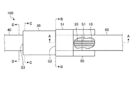
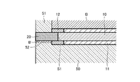
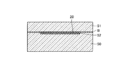
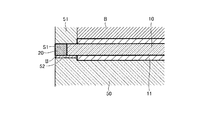
図1は、第1実施形態に係る光学モジュールの構成を示す一部破断図であり、テープ心線の内部の構成を露出させて記載している。図2は、図1におけるA−A線断面を示す断面図であり、図3は、図1におけるB−B線断面を示す断面図であり、図4は、図1におけるC−C線断面を示す断面図であり、図5は、図1におけるD−D線断面を示す断面図である。
Δ={(nc1−nc)/nc1}×100
ただし、nc1はコアの最大屈折率、ncはクラッドの屈折率であり、この比屈折率差は、高比屈折率差光ファイバ20と平面光波回路30とシリコン細線導波路40に対しても同様に定義される。
Δ1<Δ2<Δ3<Δ4
という関係が満たされている。
ここで、図6および図7を参照しながら、第1実施形態に係る光学モジュール100の変形例について説明する。図6は、変形例に係る光学モジュールの構成を示す一部破断図であり、テープ心線の内部の構成を露出させて記載している。図7は、図6におけるA’−A’線断面を示す断面図である。なお、変形例に係る光学モジュール100aは、第1実施形態に係る光学モジュール100と共通の構成が多いので、ここでは相違する構成のみ説明する。
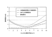
ここで、図8を参照しながら、第1実施形態に係る光学モジュール100の構成が、シングルモード光ファイバ10とシリコン細線導波路40との間の接続損失を簡便な構成で低減することができるという効果を導く作用原理について説明する。
ここで、上記説明した第1実施形態に係る光学モジュールの実施例について説明する。実施例1に係る光学モジュールは、シリコン細線導波路の両端に平面光波回路、高比屈折率差光ファイバ、シングルモード光ファイバがそれぞれ順に接続されている以外は、図1と同様に構成されており、一方のシングルモード光ファイバから入力した光を他方のシングルモード光ファイバから出力する実験用構成である。
実施例2に係る光学モジュールは、実施例1に係る光学モジュールと比較して、平面光波回路が小型化されている構成例である。
上記第1実施形態は、多心接続の光学モジュールの構成であったが、本発明の実施はこれに限定されず、単心接続の光学モジュールに対しても適用可能である。ここでは、単心接続である第2実施形態に係る光学モジュールの構成およびその接続損失の特性について説明する。ただし、第2実施形態に係る光学モジュールは、多心接続が単心接続に変更されたのみであるので、実質的に共通の構成に関しては説明を省略するものとする。
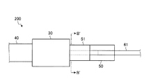
10 シングルモード光ファイバ
11,12 被覆
20 高比屈折率差光ファイバ
30 平面光波回路
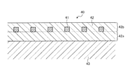
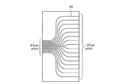
31,31c1,31c2,31e1,31e2,41 コア
32,42 クラッド
32a,42a 下部クラッド
32b,42b 上部クラッド
33,43 基板
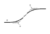
34 S字導波路
35 補助導波路
40 シリコン細線導波路
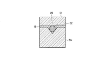
50 固定部材
51 上板
52 V字溝
60 光ファイバテープ心線
61 光ファイバ心線
Claims (10)
- シングルモード光ファイバと、
前記シングルモード光ファイバよりも、クラッドに対するコアの比屈折率差が大きく、前記シングルモード光ファイバと融着接続された高比屈折率差光ファイバと、
石英系ガラスからなるクラッドと前記石英系ガラスに屈折率を高めるドーパントを添加したコアとを有し、前記コアによって光を導波する光導波路が前記シングルモード光ファイバと融着接続されていない側の前記高比屈折率差光ファイバの端面に接続された平面光波回路と、
シリコンからなるコアと前記コアよりも屈折率が低いクラッドとを有し、前記コアによって光を導波するシリコン細線導波路が前記高比屈折率差光ファイバと接続されていない側の平面光波回路の端面における光導波路に接続されたシリコン細線導波路素子と、
を備えることを特徴とする光学モジュール。 - 前記シングルモード光ファイバにおけるクラッドに対するコアの比屈折率差をΔ1とし、前記高比屈折率差光ファイバにおけるクラッドに対するコアの比屈折率差をΔ2とし、前記平面光波回路におけるクラッドに対するコアの比屈折率差をΔ3とし、前記シリコン細線導波路におけるクラッドに対するコアの比屈折率差をΔ4とすると、
Δ1<Δ2<Δ3<Δ4
という関係を満たすことを特徴とする請求項1に記載の光学モジュール。 - 前記平面光波回路の比屈折率差であるΔ3は、4%≦Δ3≦6%であることを特徴とする請求項1または請求項2に記載の光学モジュール。
- 前記平面光波回路のコアに添加したドーパントは、ジルコニアであることを特徴とする請求項1から請求項3のうち何れか1項に記載の光学モジュール。
- 前記平面光波回路に形成された光導波路のうち、曲げ導波路の外周に沿った領域には、前記曲げ導波路を伝搬する光の曲げ損失を抑制する補助導波路が形成されていることを特徴とする請求項1から請求項4のうち何れか1項に記載の光学モジュール。
- 前記平面光波回路に形成された光導波路は、初期値として与えられた光導波路形状を微小変化させ、当該微小変化を繰り返しながら光導波路の損失を計算することにより、所望の損失を実現するものとして特定された形状であることを特徴とする請求項1から請求項5のうち何れか1項に記載の光学モジュール。
- 前記シングルモード光ファイバおよび前記高比屈折率差光ファイバは、複数本がアレイ状に配列された状態で前記平面光波回路の対応する光導波路に接続されていることを特徴とする請求項1から請求項6のうち何れか1項に記載の光学モジュール。
- 前記平面光波回路に対する前記複数本の高比屈折率差光ファイバの相対的位置を固定するための固定部材をさらに備え、
前記高比屈折率差光ファイバは、前記固定部材に設けられたV字溝と前記固定部材が備える上板とに挟持される部分の被覆が除去された状態で、前記固定部材に固定される、
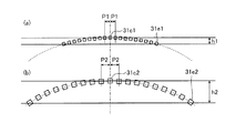
ことを特徴とする請求項7に記載の光学モジュール。 - 前記平面光波回路は、前記高比屈折率差光ファイバに接続される端面におけるコア間の間隔よりも、前記シリコン細線導波路素子に接続される端面におけるコア間の間隔の方が狭くなるように複数のS字導波路が配列された構成であることを特徴とする請求項7または請求項8に記載の光学モジュール。
- 前記平面光波回路または前記シリコン細線導波路素子は、導波する光のスポットサイズを変換するためのスポットサイズコンバータを備えることを特徴とする請求項1から請求項9のうち何れか1項に記載の光学モジュール。
Priority Applications (3)
| Application Number | Priority Date | Filing Date | Title |
|---|---|---|---|
| JP2016080592A JP6706859B2 (ja) | 2016-04-13 | 2016-04-13 | 光学モジュール |
| PCT/JP2017/009877 WO2017179352A1 (ja) | 2016-04-13 | 2017-03-13 | 光学モジュール |
| US16/150,883 US10634846B2 (en) | 2016-04-13 | 2018-10-03 | Optical module |
Applications Claiming Priority (1)
| Application Number | Priority Date | Filing Date | Title |
|---|---|---|---|
| JP2016080592A JP6706859B2 (ja) | 2016-04-13 | 2016-04-13 | 光学モジュール |
Publications (2)
| Publication Number | Publication Date |
|---|---|
| JP2017191214A true JP2017191214A (ja) | 2017-10-19 |
| JP6706859B2 JP6706859B2 (ja) | 2020-06-10 |
Family
ID=60041725
Family Applications (1)
| Application Number | Title | Priority Date | Filing Date |
|---|---|---|---|
| JP2016080592A Active JP6706859B2 (ja) | 2016-04-13 | 2016-04-13 | 光学モジュール |
Country Status (3)
| Country | Link |
|---|---|
| US (1) | US10634846B2 (ja) |
| JP (1) | JP6706859B2 (ja) |
| WO (1) | WO2017179352A1 (ja) |
Cited By (5)
| Publication number | Priority date | Publication date | Assignee | Title |
|---|---|---|---|---|
| JP2020030333A (ja) * | 2018-08-23 | 2020-02-27 | 住友電工デバイス・イノベーション株式会社 | 光90°ハイブリッド素子 |
| JP2020064211A (ja) * | 2018-10-18 | 2020-04-23 | 日本電信電話株式会社 | 光接続構造 |
| JP2020126128A (ja) * | 2019-02-04 | 2020-08-20 | 日本電信電話株式会社 | インタポーザ回路 |
| JP2020134601A (ja) * | 2019-02-14 | 2020-08-31 | 古河電気工業株式会社 | 光導波路回路 |
| CN111801612A (zh) * | 2018-03-29 | 2020-10-20 | 古河电气工业株式会社 | 光学连接部件 |
Families Citing this family (1)
| Publication number | Priority date | Publication date | Assignee | Title |
|---|---|---|---|---|
| JP6706859B2 (ja) * | 2016-04-13 | 2020-06-10 | 古河電気工業株式会社 | 光学モジュール |
Citations (3)
| Publication number | Priority date | Publication date | Assignee | Title |
|---|---|---|---|---|
| JPH05173030A (ja) * | 1991-12-20 | 1993-07-13 | Nec Eng Ltd | 光導波路の曲がり構造 |
| JP2005070284A (ja) * | 2003-08-22 | 2005-03-17 | Ricoh Printing Systems Ltd | 光導波路型光記録装置の光導波路モジュール |
| WO2015089830A1 (zh) * | 2013-12-20 | 2015-06-25 | 华为技术有限公司 | 光波导与单模光纤的耦合方法和耦合装置 |
Family Cites Families (12)
| Publication number | Priority date | Publication date | Assignee | Title |
|---|---|---|---|---|
| EP1393105A4 (en) * | 2001-04-12 | 2006-03-22 | Omniguide Inc | FIBER WAVEGUIDES WITH HIGH CONTRAST INDEX AND APPLICATIONS |
| US20030174956A1 (en) * | 2002-03-13 | 2003-09-18 | Jean-Francois Viens | Polarization insensitive modal field transformer for high index contrast waveguide devices |
| JP2007072433A (ja) * | 2005-08-11 | 2007-03-22 | Ricoh Co Ltd | 光集積素子及び光制御素子 |
| JP2007147982A (ja) * | 2005-11-28 | 2007-06-14 | Seikoh Giken Co Ltd | 光ファイバアレイおよびその製造方法 |
| JP4469871B2 (ja) * | 2007-03-28 | 2010-06-02 | 株式会社東芝 | 光導波路 |
| JP4886627B2 (ja) * | 2007-07-31 | 2012-02-29 | 株式会社東芝 | 光結合デバイス |
| US8483528B2 (en) * | 2008-02-29 | 2013-07-09 | Google Inc. | Optical mode transformer, in particular for coupling an optical fiber and a high-index contrast waveguide |
| WO2012088610A1 (en) * | 2010-12-29 | 2012-07-05 | Socpra Sciences Et Génie S.E.C. | Low loss directional coupling between highly dissimilar optical waveguides for high refractive index integrated photonic circuits |
| EP3111262B1 (en) * | 2014-02-28 | 2022-05-04 | Ciena Corporation | High index element-based spot-size converter for optical mode conversion and evanescent coupling between two waveguides |
| US20150277036A1 (en) * | 2014-03-28 | 2015-10-01 | Futurewei Technologies, Inc. | Apparatus and Method for an Optical Waveguide Edge Coupler for Photonic Integrated Chips |
| EP2950124A1 (en) * | 2014-05-28 | 2015-12-02 | Paul Scherrer Institut | Integrated photonic nanowires-based waveguide |
| JP6706859B2 (ja) * | 2016-04-13 | 2020-06-10 | 古河電気工業株式会社 | 光学モジュール |
-
2016
- 2016-04-13 JP JP2016080592A patent/JP6706859B2/ja active Active
-
2017
- 2017-03-13 WO PCT/JP2017/009877 patent/WO2017179352A1/ja active Application Filing
-
2018
- 2018-10-03 US US16/150,883 patent/US10634846B2/en active Active
Patent Citations (3)
| Publication number | Priority date | Publication date | Assignee | Title |
|---|---|---|---|---|
| JPH05173030A (ja) * | 1991-12-20 | 1993-07-13 | Nec Eng Ltd | 光導波路の曲がり構造 |
| JP2005070284A (ja) * | 2003-08-22 | 2005-03-17 | Ricoh Printing Systems Ltd | 光導波路型光記録装置の光導波路モジュール |
| WO2015089830A1 (zh) * | 2013-12-20 | 2015-06-25 | 华为技术有限公司 | 光波导与单模光纤的耦合方法和耦合装置 |
Non-Patent Citations (2)
| Title |
|---|
| TOKUSHIMA,M. ET AL.: "Dual-Tapered 10-μm-Spot-Size Converter with Double Core for Coupling Polarization-Independent Silic", APPLIED PHYSICS EXPRESS, vol. 5, JPN6019047066, 2012, pages 1 - 02202, ISSN: 0004165220 * |
| 高橋正典,外3名: "ZrO2-SiO2系高△PLCを用いたマルチキャストスイッチの開発", 古河電工時報, JPN6019047067, February 2016 (2016-02-01), pages 20 - 24, ISSN: 0004165221 * |
Cited By (9)
| Publication number | Priority date | Publication date | Assignee | Title |
|---|---|---|---|---|
| CN111801612A (zh) * | 2018-03-29 | 2020-10-20 | 古河电气工业株式会社 | 光学连接部件 |
| CN111801612B (zh) * | 2018-03-29 | 2022-11-04 | 古河电气工业株式会社 | 光学连接部件 |
| JP2020030333A (ja) * | 2018-08-23 | 2020-02-27 | 住友電工デバイス・イノベーション株式会社 | 光90°ハイブリッド素子 |
| JP2020064211A (ja) * | 2018-10-18 | 2020-04-23 | 日本電信電話株式会社 | 光接続構造 |
| US11934010B2 (en) | 2018-10-18 | 2024-03-19 | Nippon Telegraph And Telephone Corporation | Optical connection structure |
| JP2020126128A (ja) * | 2019-02-04 | 2020-08-20 | 日本電信電話株式会社 | インタポーザ回路 |
| JP7208498B2 (ja) | 2019-02-04 | 2023-01-19 | 日本電信電話株式会社 | インタポーザ回路 |
| JP2020134601A (ja) * | 2019-02-14 | 2020-08-31 | 古河電気工業株式会社 | 光導波路回路 |
| JP7042763B2 (ja) | 2019-02-14 | 2022-03-28 | 古河電気工業株式会社 | 光導波路回路 |
Also Published As
| Publication number | Publication date |
|---|---|
| WO2017179352A1 (ja) | 2017-10-19 |
| US20190033526A1 (en) | 2019-01-31 |
| JP6706859B2 (ja) | 2020-06-10 |
| US10634846B2 (en) | 2020-04-28 |
Similar Documents
| Publication | Publication Date | Title |
|---|---|---|
| WO2017179352A1 (ja) | 光学モジュール | |
| KR101121459B1 (ko) | 광섬유 및 평면 광학 도파관을 치밀하게 결합하는 방법 및장치 | |
| US7509010B2 (en) | End-surface closely arranged multicore optical fiber and manufacturing method thereof | |
| CN112180498A (zh) | 多芯光纤 | |
| US10007073B2 (en) | Optical component including a high-relative-refractive-index-index-difference optical fiber a single-mode optical fiber an optical device and a fixing member to fix a relative opsition | |
| US11828978B2 (en) | Multi-core optical fiber and multi-core optical fiber cable | |
| US11860406B2 (en) | Optical fiber | |
| JP2006337550A (ja) | 光結合器 | |
| JP2008040094A (ja) | 回折格子及び分散補償回路 | |
| WO2021090912A1 (ja) | 光ファイバ | |
| US11808972B2 (en) | Optical fiber | |
| JP2020204642A (ja) | 光源モジュール | |
| US6920266B2 (en) | Integrated optical directional coupler | |
| WO2021149589A1 (ja) | 光部品 | |
| WO2022044101A1 (ja) | 光導波路部品およびその製造方法 | |
| JP2016212414A (ja) | 導波路用結合回路 | |
| WO2019117313A1 (ja) | 光偏波素子およびその製造方法 | |
| Presby et al. | Packaging of glass waveguide silicon devices | |
| JP4569440B2 (ja) | 温度無依存光合分波器 | |
| US20030053775A1 (en) | Optical fiber adapted for interfacing | |
| JP2006106372A (ja) | 光分岐装置 | |
| JP2019159127A (ja) | ファイバモジュール | |
| CN112379478B (zh) | 一种基于亚波长光栅结构的弯曲波导及设计方法 | |
| GB2565128A (en) | Fan-in/Fan-out device | |
| WO2022085245A1 (ja) | 光ファイバケーブル |
Legal Events
| Date | Code | Title | Description |
|---|---|---|---|
| A621 | Written request for application examination |
Free format text: JAPANESE INTERMEDIATE CODE: A621 Effective date: 20190219 |
|
| A131 | Notification of reasons for refusal |
Free format text: JAPANESE INTERMEDIATE CODE: A131 Effective date: 20191203 |
|
| A521 | Request for written amendment filed |
Free format text: JAPANESE INTERMEDIATE CODE: A523 Effective date: 20200129 |
|
| TRDD | Decision of grant or rejection written | ||
| A01 | Written decision to grant a patent or to grant a registration (utility model) |
Free format text: JAPANESE INTERMEDIATE CODE: A01 Effective date: 20200428 |
|
| A61 | First payment of annual fees (during grant procedure) |
Free format text: JAPANESE INTERMEDIATE CODE: A61 Effective date: 20200515 |
|
| R151 | Written notification of patent or utility model registration |
Ref document number: 6706859 Country of ref document: JP Free format text: JAPANESE INTERMEDIATE CODE: R151 |
|
| S531 | Written request for registration of change of domicile |
Free format text: JAPANESE INTERMEDIATE CODE: R313531 |
|
| R350 | Written notification of registration of transfer |
Free format text: JAPANESE INTERMEDIATE CODE: R350 |