WO2017170931A1 - 撮像装置及び検査装置 - Google Patents
撮像装置及び検査装置 Download PDFInfo
- Publication number
- WO2017170931A1 WO2017170931A1 PCT/JP2017/013397 JP2017013397W WO2017170931A1 WO 2017170931 A1 WO2017170931 A1 WO 2017170931A1 JP 2017013397 W JP2017013397 W JP 2017013397W WO 2017170931 A1 WO2017170931 A1 WO 2017170931A1
- Authority
- WO
- WIPO (PCT)
- Prior art keywords
- soldering
- imaging
- workpiece
- air
- inspection
- Prior art date
- Legal status (The legal status is an assumption and is not a legal conclusion. Google has not performed a legal analysis and makes no representation as to the accuracy of the status listed.)
- Ceased
Links
Images










Classifications
-
- B—PERFORMING OPERATIONS; TRANSPORTING
- B23—MACHINE TOOLS; METAL-WORKING NOT OTHERWISE PROVIDED FOR
- B23K—SOLDERING OR UNSOLDERING; WELDING; CLADDING OR PLATING BY SOLDERING OR WELDING; CUTTING BY APPLYING HEAT LOCALLY, e.g. FLAME CUTTING; WORKING BY LASER BEAM
- B23K1/00—Soldering, e.g. brazing, or unsoldering
-
- G—PHYSICS
- G01—MEASURING; TESTING
- G01N—INVESTIGATING OR ANALYSING MATERIALS BY DETERMINING THEIR CHEMICAL OR PHYSICAL PROPERTIES
- G01N21/00—Investigating or analysing materials by the use of optical means, i.e. using sub-millimetre waves, infrared, visible or ultraviolet light
- G01N21/84—Systems specially adapted for particular applications
- G01N21/88—Investigating the presence of flaws or contamination
- G01N21/95—Investigating the presence of flaws or contamination characterised by the material or shape of the object to be examined
- G01N21/956—Inspecting patterns on the surface of objects
-
- H—ELECTRICITY
- H05—ELECTRIC TECHNIQUES NOT OTHERWISE PROVIDED FOR
- H05K—PRINTED CIRCUITS; CASINGS OR CONSTRUCTIONAL DETAILS OF ELECTRIC APPARATUS; MANUFACTURE OF ASSEMBLAGES OF ELECTRICAL COMPONENTS
- H05K3/00—Apparatus or processes for manufacturing printed circuits
- H05K3/30—Assembling printed circuits with electric components, e.g. with resistors
- H05K3/32—Assembling printed circuits with electric components, e.g. with resistors electrically connecting electric components or wires to printed circuits
- H05K3/34—Assembling printed circuits with electric components, e.g. with resistors electrically connecting electric components or wires to printed circuits by soldering
Definitions
- the present invention relates to an imaging apparatus and an inspection apparatus using the imaging apparatus.
- Non-contact optical inspection for confirming the presence or absence of defects in manufactured electronic components is known.
- An inspection device that determines whether soldering is good or bad is still known.
- an electronic component in which a component lead is inserted into a through hole of a substrate and soldered is called an inserted component.
- a flow soldering apparatus is used for soldering the insertion part. In the soldering process, poor soldering such as bridges and non-wetting occurs due to various causes. For this reason, the inspection after the mounting process is indispensable.
- an appearance inspection device that uses an imaging device, a laser, an X-ray, or the like to determine whether soldering is good or bad is known.
- Patent Document 1 describes an inspection apparatus that inspects a soldering surface of a component mounting board that has undergone a flow soldering process using an imaging apparatus.
- an object of the present invention is to provide an imaging apparatus and an inspection apparatus that can prevent such erroneous determination and reduce a load such as maintenance work of a worker.
- the present invention is an image pickup apparatus having an image pickup element, an image pickup lens, and an air outlet that forms an air flow across the front surface of the image pickup lens. Preferably, it has a suction port for sucking airflow.
- the present invention includes an imaging device having an imaging device, an imaging lens, and an air outlet that forms an airflow across the front surface of the imaging lens, and inspects an object using an imaging signal of the imaging device It is.
- the imaging device images the soldering surface of the workpiece to which the component is soldered, inspects the soldering failure from the imaging signal of the imaging device, and stores the soldering failure location.
- the workpiece is one in which components are soldered to the substrate by flow soldering.
- the inspection position has another air outlet that forms an air flow toward the soldering surface of the substrate.
- the inspection position has a suction port for sucking airflow.
- the temperature of the airflow toward the soldering surface of the substrate is set higher than the airflow across the lens front surface.
- the present invention it is possible to prevent dust from adhering to the front surface of the imaging device and to blow off the adhering dust. Also, fumes drifting like smoke around the work can be blown away. Therefore, when inspecting based on the captured image of the imaging device, it is possible to prevent a normal one from being erroneously determined as defective.
- the effect described here is not necessarily limited, and any effect described in this invention may be sufficient. Further, the contents of the present invention are not construed as being limited by the effects exemplified in the following description.
- FIG. 1 is a plan view showing a configuration of an imaging apparatus and its periphery in an embodiment of the present invention.
- FIG. 1 is a front view illustrating a configuration of an imaging apparatus and its periphery according to an embodiment of the present invention.
- FIG. 1 is a partial cross-sectional view illustrating a configuration of an imaging apparatus and its periphery according to an embodiment of the present invention.
- FIG. 1 is a partial cross-sectional view illustrating a configuration of an imaging apparatus and its periphery according to an embodiment of the present invention. It is a perspective view which shows the structure of an imaging device and its periphery. It is a front view which shows the structure at the time of an external appearance test
- Embodiments of the present invention will be described below. The description will be given in the following order. ⁇ 1. Flow soldering apparatus to which this invention can be applied> ⁇ 2. Embodiment> ⁇ 3. Modification> The embodiment described below is a preferred specific example of the present invention, and various technically preferable limitations are given. However, the scope of the present invention is particularly limited to the present invention in the following description. Unless otherwise stated, the present invention is not limited to these embodiments.
- FIG. 1 shows the configuration of the entire system of a flow soldering apparatus to which the present invention can be applied.
- the workpiece W is carried into a flux coating device (hereinafter referred to as a fluxer as appropriate) 1.
- a fluxer as appropriate
- the lead of the insertion component is inserted into the through hole on the substrate on which the chip component or the like is surface-mounted.
- a substrate to which the insertion component is attached is a workpiece W.
- the work W is a term including a silicon wafer and the like in addition to the printed wiring board.
- the fluxer 1 is, for example, a spray fluxer that applies a flux only to a necessary portion.
- the preheater 2 and the soldering device 3 are arranged inline with respect to the fluxer 1.
- the workpiece W is placed on a conveyor and conveyed to each device.
- the preheater 2 preheats the workpiece W, and the workpiece W is heated to about 100 ° C., for example.
- the soldering device 3 is a device that performs flow soldering.
- An example of the flow soldering method performed in the soldering apparatus 3 is a flow method in which the workpiece W is passed over the jetted solder to perform soldering.
- a method capable of performing selective soldering in which solder is jetted only in a necessary region without jetting solder on the entire surface of the workpiece W may be used.
- a dip method in which the back surface of the work is immersed in a solder bath in which solder is melted and soldering may be used.
- a suitable device is a local trace soldering device.
- the local trace soldering device has a configuration in which only the location of the insertion part can be soldered in a preset order (path), and the molten solder that can flexibly accommodate the length and number of the entire insertion part lead is jetted. A jet nozzle.
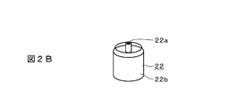
- FIG. 2A, 2B and 2C are diagrams for schematically explaining the local trace soldering apparatus.
- a jet nozzle 22 and a solder bath 23 are installed on an XY stage 21.
- the XY stage 21 can be displaced in the X direction and the Y direction by a servo motor (not shown).
- the jet nozzle 22 can be displaced also in the Z (vertical) direction.
- the jet nozzle 22 is displaced upward, and the lead protruding from the back surface of the workpiece W by the molten solder jetted from the jet nozzle 22 is formed on the substrate. Soldered in place.
- ⁇ Leads are soldered at the positions of a plurality of insertion parts in accordance with a preset order by an operation according to the insertion parts. 2A, 2B and 2C, the jet nozzle 22 is displaced in the XY direction, but the jet nozzle 22 is fixed and the workpiece W is displaced in the XY and Z directions. May be.
- the jet nozzle 22 has a nozzle 22a and a cylinder 22b concentrically surrounding the nozzle 22a.
- the molten solder supplied from the solder bath 23 jets upward from the opening at the tip of the nozzle 22a, contacts the soldering location on the back surface of the workpiece W, and is soldered.
- the molten solder spilled from the nozzle 22a returns to the lower solder tank 23 from the opening of the cylinder 22b.
- the solder bath 23 is provided with a rotating blade, a power source (motor), and the like for forming a solder flow, and circulates the molten solder.
- the lead 26 of the insertion component 25 is inserted into the substrate 24.
- the jet nozzle 22 moves in a direction parallel to the arrangement direction on one side of the lead 26, and the soldering of the lead 26 is corrected by the solder 27 jetted from the nozzle 22a.
- the soldering correction of the lead on one side is completed, the soldering correction is similarly performed on the lead on the other side.
- the bridge can be satisfactorily corrected by making the moving direction of the jet nozzle 22 parallel to the direction of occurrence of the bridge.
- the mounted workpiece W is transferred to the first appearance inspection device 4 by the soldering device 3, and a soldering defect inspection is performed in a non-contact manner.
- the appearance inspection apparatus 4 captures the mounting surface (soldering surface) of the workpiece W by an imaging device, and an operator looks at the image to determine a defect, or the image is processed by digital signal processing. An automatic determination method can be used.
- the soldering device 3 and the appearance inspection device 4 are shown separately above and below, but this is for easy understanding of the features of the present invention. That is, the appearance inspection device 4 is arranged in line with the soldering device 3, and the workpiece W is continuously conveyed from the soldering device 3 to the appearance inspection device 4.
- the correction device 5 is arranged inline with respect to the appearance inspection device 4.
- the coordinates of the position of the poorly soldered insertion part discovered by the previous appearance inspection apparatus 4 (referred to as defect position information 7 as appropriate) are supplied to the correction apparatus 5.
- the correction device 5 corrects the soldering defect according to the received defect position information 7.
- the corrected workpiece W is conveyed to the second appearance inspection device 6 for final inspection.
- the appearance inspection device 6 can be the same as the appearance inspection device 4.
- the work carried out from the appearance inspection apparatus 6 is used for the next step.
- the work for which the final appearance inspection apparatus 6 has found a soldering defect may be repaired again and repaired, or may be discarded.
- the defect position information obtained by the appearance inspection apparatus 6 is used.
- the preheater 2, the soldering device 3, the appearance inspection device 4, the correction device 5, and the appearance inspection device 6 may be configured as modules that can be separated from each other.
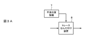
- FIG. 3A shows an example in which the correction device 5 is configured by a local trace soldering device 8.
- the defect position information 7 obtained by the appearance inspection device 4 is supplied to the local trace soldering device 8.
- the local trace soldering apparatus 8 solders only the portion of the insertion part that is poorly soldered.
- the soldering operation (path and the like) of the local trace soldering device 8 is determined based on the defect position information.
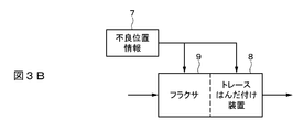
- FIG. 3B shows an example in which the correction device 5 is configured by a local trace soldering device 8 and a fluxer 9.
- the fluxer 9 is, for example, a spray fluxer, and defect position information is supplied to the fluxer 9 and flux is applied only to the defective portion.
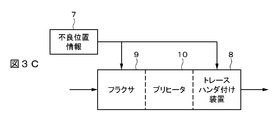
- FIG. 3C shows an example in which the correction device 5 is constituted by a local trace soldering device 8, a fluxer 9, and a preheater 10.
- the fluxer 9 is, for example, a spray fluxer, and defect position information is supplied to the fluxer 9 and flux is applied only to the defective portion.
- the workpiece W from the fluxer 9 is preheated by the preheater 10 and supplied to the local trace soldering device 8.
- 3A, 3B, and 3C can be selected in consideration of the type of soldering failure to use as the correction device 5.
- the correction device 5 having the configuration as shown in FIG. 3C is installed, and control is performed to selectively operate / inactivate (only pass) each of the fluxer 9 and the preheater 10 according to the type of soldering failure. You may do it.
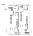
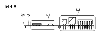
- FIG. 4B shows a cross-sectional view along line AA of the workpiece W shown in FIG. 4A.
- a portion surrounded by a line L1 is a mounting region for a surface mounting component
- a portion surrounded by a line L2 is a mounting region for an insertion component.
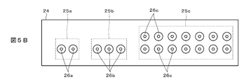
- 5A is an enlarged view of the cross-section of the mounting area (the portion surrounded by the line L2) of the insertion component. Furthermore, the top view of the soldering surface of the area
- the leads 26a, 26b, and 26c of the insertion parts 25a, 25b, and 25c are inserted into the through holes of the substrate 24, and the leads 26a, 26b, and 26c are soldered to the substrate 24 by flow soldering.
- 5A and 5B are diagrams in the case where no soldering failure occurs.
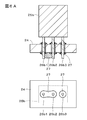
- FIG. 6A is a cross-sectional view showing a bridge (short) which is an example of a soldering failure and a plan view of a soldering surface.
- a bridge short
- FIG. 6A is a cross-sectional view showing a bridge (short) which is an example of a soldering failure and a plan view of a soldering surface.
- FIG. 6B is a sectional view showing non-wetting (unsoldered), which is another example of a soldering failure, and a plan view of the soldering surface.
- the solder 27 is not sufficiently attached to the lead 26b1 of the insertion component 25b. Solder is supplied to the lead 26b1 by the correcting device 5, and non-wetting (unsoldered) is eliminated.
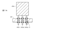
- FIG. 7A, 7B, and 7C are a cross-sectional view (FIG. 7A) showing a blow hole, which is still another example of a soldering failure, a plan view of a soldering surface (FIG. 7B), and a C-part enlarged cross-sectional view (FIG. 7C).
- the solder 27 is attached to the lead 26b3 of the insertion part 25b, but a small spherical blow hole 28 is formed in a part of the soldering portion.
- the lead 26b3 is soldered again by the correction device 5, and the blow hole 28 is eliminated.
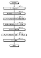
- Step ST1 A mounted work is input to the appearance inspection apparatus 4.
- Step ST2 An appearance inspection is performed by the appearance inspection apparatus 4.
- Step ST3 The presence or absence of soldering defects is examined.
- Step ST4 If it is determined in step ST3 that there is no soldering defect, the process proceeds to the next step.
- Step ST5 If it is determined in step ST3 that there is a soldering defect, the coordinates of the defective part are stored as defect position information.
- Step ST6 The correction device 5 corrects the defective part using the defect position information.
- Step ST7 The appearance inspection apparatus 6 determines whether or not there is a final defect. If it is determined that there is no defect, the process proceeds to the next process (step ST4). If it is determined that there is a defect, the workpiece is again input to the appearance inspection apparatus 4, and the above-described processing is repeated.
- a defective workpiece may be placed in a stocker and discarded. Furthermore, the work of FIG. 8 and the process of FIG. 9 may be combined to discard a workpiece that remains defective even if it is corrected twice or more.
- Embodiment> “Configuration of imaging device and its surroundings”
- the present invention is applied to the appearance inspection apparatus in the above-described flow soldering system.
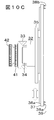
- 10A to 10D are a plan view, a front view, and a partial cross-sectional view of the imaging apparatus according to the embodiment
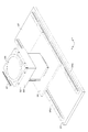
- FIG. 11 is a perspective view of the imaging apparatus
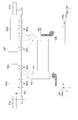
- FIG. 12 shows a configuration during an appearance inspection.
- the imaging device 32 is an industrial camera, and an imaging device (not shown) and a lens 34 are provided in a cylinder 33.
- the imaging device 32 images the soldering surface of the workpiece W from the bottom upward. That is, it is determined from the imaging signal of the imaging device 32 whether or not the above-described defect such as a bridge has occurred on the soldering surface.
- the imaging device 32 is mounted on the xy stage.
- the xy stage has, for example, a moving plate 35 in the y direction, guide rails 36a and 36b in the y direction, a moving plate 37 in the x direction, and guide rails 38a and 38b in the x direction. Note that a stepping motor, a position detection sensor, and the like as a drive source of the xy stage are omitted.
- the imaging device 32 is mounted on the moving plate 35, and the slider on the lower surface of the moving plate 35 is guided by the guide rails 36a and 36b.
- Guide rails 36 a and 36 b are provided in parallel on the moving plate 37.
- the slider on the lower surface of the moving plate 37 is guided by guide rails 38a and 38b.
- Guide rails 38 a and 38 b are provided on the base plate 39 in parallel.
- the imaging device 32 can be displaced in the x and y directions by an xy stage. In FIG. 11, the guide rails 38a and 38b and the base plate 39 are not shown.
- An air outlet 41 for blowing air to the front surface of the lens 34 around the lens 34 of the imaging device 32 is provided.
- a linear air outlet 41 having a length equal to or longer than the diameter of the front surface of the lens 34 is provided on the side surface of the tube 33.
- An air suction port 43 that is opposed to the air blowing port 41 across the front surface of the lens 34 is provided.
- the airflow formed by blowing air from the air blowing port 41 passes through the front surface of the lens 34 in the x direction and is sucked by the air suction port 43. Accordingly, dust adhering to the front surface of the lens 34 is blown away by the air current.
- the air suction port 43 is connected to a duct (not shown), and sucked fume, dust, and the like are exhausted outside the work place through the duct.
- FIG. 11 illustration of the other air blowing port 42 and the air suction port 43 is abbreviate
- the flux fume from the workpiece W immediately after soldering is not only blown away by the air flow from the air blowing ports 41 and 42, but is also collected more effectively by being sucked by the air suction port 43. .
- the leads 26d, 26e, 26f of the insertion parts 25d, 25e, 25f are inserted into the through holes of the substrate 24, and the leads 26d, 26e, 26f are obtained by flow soldering. Is soldered to the substrate 24.
- the workpiece W is transported in a direction orthogonal to the drawing by the transport conveyors 31a and 31b.
- the appearance inspection apparatus is configured in a box-shaped casing, and the workpiece W is introduced into the casing by the transfer conveyors 31a and 31b, and the workpiece W is stopped at a predetermined position for inspection (referred to as an inspection position as appropriate). .
- the work W is clamped on both sides as necessary during inspection.
- the imaging device 32 images the soldering surface of the workpiece W and analyzes the imaging signal to inspect the soldering quality.
- the two air outlets 41 and 42 are configured such that a large number of small outlets are linearly arranged in the y direction, and the air inlet 43 is used in common with the air outlets 41 and 42. ing.
- the air blowing ports 41 and 42 have different air blowing directions, but the air flow is substantially in the x direction. Therefore, the air from each air outlet 41 and 42 does not interfere and weaken the momentum of the flow. Furthermore, the air from the air outlet 41 and the air from the air outlet 42 may be the same, or the temperature of the air blown out from the air outlet 42 may be made higher.
- the temperature of the air blown out from the air outlet 42 is increased, so that when the defective portion of the workpiece W after the appearance inspection is corrected by the correction device, it can be used as a preheater for the soldering surface of the workpiece W. Therefore, it becomes possible to correct the defective portion more reliably.
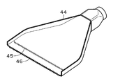
- a fan-shaped nozzle 44 having an outlet (or suction inlet) 45 and an outlet 46 at the tips can be used.
- the nozzle 44 is made of, for example, resin or metal. Air from an air source (for example, factory air) is introduced from the base of the nozzle 44. A nozzle having the same shape as in FIG. 13 can be used as the air suction port 43. For example, air is sucked in by an ejector.
- System configuration A connection configuration of the inspection apparatus according to the embodiment of the present invention will be described with reference to FIG.
- An imaging signal obtained by the imaging device 32 is supplied to the personal computer 51 that controls the entire system via an analog or digital interface.
- the personal computer 51 controls the xy stage 52 to control the position of the imaging device 32 with respect to the workpiece W.
- the work W is divided into a plurality of areas, and the quality of soldering is inspected for each area.
- the inspection is performed by image processing by the personal computer 51.
- Information on the obtained defective portion is transmitted to the correction device at the next stage by wire or wirelessly.
- the personal computer 51 controls the air control unit 53, and at the time of inspection, the air control unit 53 turns on, for example, an electromagnetic valve to blow out air from the air blowing ports 41 and 42.
- the air control unit 53 also has a function of controlling a suction machine, for example, an ejector, and suction is performed in parallel with air blowing.
- the personal computer 51 controls the work conveyance unit 54 to carry in the work W to the inspection position, fix the work W at the inspection position, and carry out the work W after completion of the inspection.
- An operator operates the input device 55 for the personal computer 51 to cause the inspection device to perform a desired operation. Further, an image captured by the imaging device 32, a user interface screen, and the like are displayed on the display device 56.
- Step ST11 The workpiece W is carried into the inspection position, moved to the inspection position by the workpiece conveyance unit 54, and further the workpiece W is fixed.
- Step ST12 The imaging device 32 (denoted as a camera in FIG. 15) is moved to the inspection position by the xy stage.
- Step ST13 The object (the soldering surface of the workpiece W) is imaged with the imaging device 32 facing upward.
- Step ST14 The captured image is transferred to the personal computer 51.
- Step ST15 The image is analyzed by software processing in the personal computer 51, and the quality of soldering is inspected.
- Step ST16 The information obtained in step ST15 is transferred to the subsequent correction device.
- Step ST17 The workpiece W is carried out. If there is a next workpiece to be inspected, control returns to step ST11.
- the present invention it is possible to prevent dust from adhering to the front surface of the imaging apparatus and to blow off the adhering dust. Also, fumes drifting like smoke around the work can be blown away. Therefore, when analyzing a picked-up image of the image pickup device and inspecting a soldering defect, it is possible to prevent a normal one from being erroneously determined as a defect. Furthermore, by sucking air, it is possible to prevent accumulation of unnecessary materials such as dust and fume in the inspection apparatus.
- the imaging apparatus may be moved in one direction of the x and y directions, and the work may be moved in the other direction of the x and y directions.
- an illuminating device or a flash device may be provided in the imaging device to ensure illuminance during imaging.
- the present invention may be applied to a case where an imaging device is used for a monitor inside the flow soldering apparatus.
Landscapes
- Engineering & Computer Science (AREA)
- Mechanical Engineering (AREA)
- Physics & Mathematics (AREA)
- Health & Medical Sciences (AREA)
- Life Sciences & Earth Sciences (AREA)
- Chemical & Material Sciences (AREA)
- Analytical Chemistry (AREA)
- Biochemistry (AREA)
- General Health & Medical Sciences (AREA)
- General Physics & Mathematics (AREA)
- Immunology (AREA)
- Pathology (AREA)
- Manufacturing & Machinery (AREA)
- Microelectronics & Electronic Packaging (AREA)
- Electric Connection Of Electric Components To Printed Circuits (AREA)
- Investigating Materials By The Use Of Optical Means Adapted For Particular Applications (AREA)
Abstract
撮像信号を使用して対象物の検査を正確に行うことを可能とする。撮像素子と、撮像レンズと、撮像レンズの前面を横切る気流を形成する吹き出し口とを有する撮像装置である。また、撮像素子と、撮像レンズと、撮像レンズの前面を横切る気流を形成する吹き出し口とを有する撮像装置とを有し、撮像装置の撮像信号を使用して対象物の検査を行う検査装置である。
Description
この発明は、撮像装置及び撮像装置を使用した検査装置に関する。
製造された電子部品に関して不良の有無を確認する非接触光学的検査(以下、外観検査と適宜称する)が知られている。まだ、はんだ付けの良否を判定する検査装置が知られている。例えば基板のスルーホールに部品のリードを挿入してはんだ付けする電子部品は、挿入部品と呼ばれる。挿入部品のはんだ付けは、一般的には、フローはんだ付け装置が使用される。はんだ付け工程では、種々の原因によって例えばブリッジや不濡れ等のはんだ付け不良が発生する。このため、実装工程後の検査が不可欠であった。検査方法の一つとして、撮像装置、レーザ、X線等を使用してはんだ付けの良否を判定する外観検査装置が知られている。例えば特許文献1には、フローはんだ付け工程を経た部品実装基板のはんだ付け面を撮像装置によって検査する検査装置が記載されている。
特許文献1に記載されているように、はんだ付け面を下側から撮像装置によって撮像する場合、撮像装置が上向きであるために撮像装置の前面(レンズ表面)に塵埃が付着しやすい。塵埃によってはんだ付けが正常であるにもかかわらず、はんだ付けが不良と判定される誤判定の問題があった。さらに、はんだ付け装置から搬出された直後の基板は、フラックスが気化するために、ヒュームと呼ばれるガスが発生して撮像画が不鮮明となり、同様に誤判定が発生する。また基板のはんだ付けは一般的には連続的に行われるため、はんだ付けに使用されるフラックスのヒュームが撮像装置の前面(レンズ表面)に経時的に付着堆積し、その清掃等のメインテナンス作業を作業員が定期的に行う必要があった。
したがって、この発明の目的は、かかる誤判定を防止し、作業員のメインテナンス作業といった負荷を低減することができる撮像装置及び検査装置を提供することにある。
この発明は、撮像素子と、撮像レンズと、撮像レンズの前面を横切る気流を形成する吹き出し口とを有する撮像装置である。好ましくは、気流を吸い込む吸い込み口を有する。この発明は、撮像素子と、撮像レンズと、撮像レンズの前面を横切る気流を形成する吹き出し口とを有する撮像装置を有し、撮像装置の撮像信号を使用して対象物の検査を行う検査装置である。好ましくは、検査位置は、部品がはんだ付けされたワークのはんだ付け面を、撮像装置が撮像し、撮像装置の撮像信号からはんだ付け不良を検査し、はんだ付けの不良箇所を記憶する。好ましくは、ワークは、フローはんだ付けによって基板に部品がはんだ付けされたものである。好ましくは、検査位置は、基板のはんだ付け面に向かう気流を形成する他の吹き出し口を有する。好ましくは、検査位置は、気流を吸い込む吸い込み口を有する。好ましくは、レンズ前面を横切る気流に比して基板のはんだ付け面に向かう気流の温度をより高く設定する。
少なくとも一つの実施形態によれば、撮像装置の前面に塵埃が付着することを防止できると共に、付着した塵埃を吹き飛ばすことができる。また、ワークの周辺に煙のように漂っているヒュームを吹き飛ばすことができる。したがって、撮像装置の撮像画像に基づいて検査する場合に、正常なものを不良と誤判定することを防止することができる。なお、ここに記載された効果は必ずしも限定されるものではなく、この発明中に記載されたいずれの効果であってもよい。また、以下の説明における例示された効果によりこの発明の内容が限定して解釈されるものではない。
以下、この発明を実施の形態について説明する。なお、説明は、以下の順序で行う。
<1.この発明を適用できるフローはんだ付け装置>
<2.一実施の形態>
<3.変形例>
なお、以下に説明する一実施の形態は、この発明の好適な具体例であり、技術的に好ましい種々の限定が付されているが、この発明の範囲は、以下の説明において、特にこの発明を限定する旨の記載がない限り、これらの実施の形態に限定されないものとする。
<1.この発明を適用できるフローはんだ付け装置>
<2.一実施の形態>
<3.変形例>
なお、以下に説明する一実施の形態は、この発明の好適な具体例であり、技術的に好ましい種々の限定が付されているが、この発明の範囲は、以下の説明において、特にこの発明を限定する旨の記載がない限り、これらの実施の形態に限定されないものとする。
<1.この発明を適用できるフローはんだ付け装置>
図1は、この発明を適用できるフローはんだ付け装置のシステム全体の構成を示す。ワークWは、フラックス塗布装置(以下、フラクサと適宜称する)1に搬入される。図示しない部品挿入工程において、例えばチップ部品等が面実装されている基板上のスルーホールに対して挿入部品のリードが挿入される。この挿入部品が取り付けられた基板がワークWである。但し、ワークWは、プリント配線基板以外に、シリコンウェハー等も含む用語である。フラクサ1は、例えば必要な箇所にのみフラックスを塗布するスプレーフラクサである。
図1は、この発明を適用できるフローはんだ付け装置のシステム全体の構成を示す。ワークWは、フラックス塗布装置(以下、フラクサと適宜称する)1に搬入される。図示しない部品挿入工程において、例えばチップ部品等が面実装されている基板上のスルーホールに対して挿入部品のリードが挿入される。この挿入部品が取り付けられた基板がワークWである。但し、ワークWは、プリント配線基板以外に、シリコンウェハー等も含む用語である。フラクサ1は、例えば必要な箇所にのみフラックスを塗布するスプレーフラクサである。
フラクサ1に対してプリヒータ2及びはんだ付け装置3がインラインに配列されている。ワークWは、コンベア上に載置されて各装置に搬送される。プリヒータ2は、ワークWを予熱するもので、例えば100℃程度まで、ワークWが加熱される。
はんだ付け装置3は、フローはんだ付けを行う装置である。はんだ付け装置3においてなされるフローはんだ付けの方法の一例は、噴流させたはんだ上をワークWを通過させてはんだ付けを行うフロー方式である。フロー方式の場合で、ワークWの全面にはんだを噴流させないで、必要な領域に対してのみはんだを噴流させる選択的はんだ付けが可能な方法を使用しても良い。さらに、フロー方式に限らず、はんだを溶融させたはんだ槽にワーク裏面を浸漬させてはんだ付けを行うディップ方式を使用しても良い。
さらに、はんだ付け装置3として、好適な装置は、局所トレースはんだ付け装置である。局所トレースはんだ付け装置は、挿入部品の箇所のみを予め設定した順序(経路)でもってはんだ付けすることが可能な構成で、挿入部品リード全体の長さや本数にフレキシブルに対応可能な溶融はんだを噴流する噴流ノズルを有する。
図2A、図2B及び図2Cは、局所トレースはんだ付け装置を概略的に説明するための図である。図2Aに示すように、XYステージ21上に噴流ノズル22及びはんだ槽23が設置されたものである。XYステージ21は、図示しないサーボモータによってX方向及びY方向に変位可能とされている。さらに、噴流ノズル22は、Z(上下)方向にも変位可能とされている。XYステージ21と対向して噴流ノズル22の上方にワークWが位置すると、噴流ノズル22が上方に変位し、噴流ノズル22から噴流する溶融はんだによって、ワークWの裏面から突出しているリードが基板の所定箇所にはんだ付けされる。
予め設定されている順序にしたがって、複数の挿入部品の位置で、当該挿入部品に応じた動作でリードがはんだ付けされる。図2A、図2B及び図2Cの例では、噴流ノズル22がX-Y方向に変位される構成であるが、噴流ノズル22を固定し、ワークWをX-Y及びZ方向に変位させるようにしても良い。
噴流ノズル22は、図2Bに示すように、ノズル22a及びノズル22aを同心円状に取り囲む円筒22bを有する。はんだ槽23から供給された溶融はんだがノズル22aの先端の開口から上部に噴流し、ワークWの裏面のはんだ付けの箇所に接触し、はんだ付けがなされる。ノズル22aからこぼれた溶融はんだが円筒22bの開口から下部のはんだ槽23に戻る。はんだ槽23には、はんだの流れを形成するための回転羽根、動力源(モータ)等が設けられており、溶融はんだを循環させる。
図2Cに示すように、基板24に対して挿入部品25のリード26が挿入されている。リード26の片側の配列方向と平行な方向に噴流ノズル22が移動し、ノズル22aから噴流したはんだ27によって、リード26のはんだ付けの修正がなされる。片側のリードのはんだ付け修正が終了すると、他方の側のリードに対して同様にはんだ付け修正がなされる。後述するように、このように、噴流ノズル22の移動方向をブリッジの発生方向と平行とすることによってブリッジを良好に修正することができる。
図1に戻って説明すると、はんだ付け装置3によって実装済のワークWが第1の外観検査装置4に搬送され、はんだ付けの不良の検査が非接触でなされる。外観検査装置4としては、後述するように、撮像装置によってワークWの実装面(はんだ付け面)を撮像し、作業者が画像を見て不良を判定するものや、画像をデジタル信号処理で処理する自動判定方式を使用することができる。なお、図1においては、はんだ付け装置3と外観検査装置4とが分離して上下に示されているが、これは、この発明の特徴部分を分かりやすく示すためである。すなわち、はんだ付け装置3とインライン上に外観検査装置4が配列され、はんだ付け装置3から外観検査装置4に対しては、連続的にワークWが搬送される。
外観検査装置4に対して修正装置5がインラインに配置されている。前段の外観検査装置4によって発見されたはんだ付け不良の挿入部品の位置の座標(不良位置情報7と適宜称する)が修正装置5に対して供給される。修正装置5は、受け取った不良位置情報7にしたがってはんだ付け不良を修正する。
修正後のワークWが第2の外観検査装置6に搬送され、最終的な検査がなされる。外観検査装置6は、外観検査装置4と同様のものを使用することができる。外観検査装置6から搬出されたワークが次の工程に供される。最終的な外観検査装置6によってはんだ付け不良が発見されたワークについては、後述するように、再度、修正工程に供されてリペアされる場合と、廃棄される場合とがある。リペアされる場合には、外観検査装置6によって得られた不良位置情報が使用される。なお、この発明の一実施の形態において、プリヒータ2、はんだ付け装置3、外観検査装置4、修正装置5及び外観検査装置6をそれぞれ分離可能なモジュールの構成としても良い。
図3A、図3B及び図3Cを参照して修正装置5の構成例について説明する。図3Aは、修正装置5を局所トレースはんだ付け装置8によって構成する例である。局所トレースはんだ付け装置8に対しては、外観検査装置4によって得られた不良位置情報7が供給される。局所トレースはんだ付け装置8は、図2A、図2B及び図2Cを参照して説明したように、はんだ付けが不良な挿入部品の箇所のみをはんだ付けする。局所トレースはんだ付け装置8のはんだ付けの動作(経路等)は、不良位置情報に基づいて決定される。
図3Bは、修正装置5を局所トレースはんだ付け装置8及びフラクサ9によって構成する例である。フラクサ9は、例えばスプレーフラクサであって、フラクサ9に対して不良位置情報が供給され、不良箇所のみに対してフラックスが塗布される。
図3Cは、修正装置5を局所トレースはんだ付け装置8、フラクサ9及びプリヒータ10によって構成する例である。フラクサ9は、例えばスプレーフラクサであって、フラクサ9に対して不良位置情報が供給され、不良箇所のみに対してフラックスが塗布される。フラクサ9からのワークWがプリヒータ10によって予熱され、局所トレースはんだ付け装置8に供給される。なお、局所トレースはんだ付け装置8、フラクサ9、プリヒータ10をそれぞれ分離可能なモジュールの構成としても良い。
図3A、図3B及び図3Cの何れの構成を修正装置5として使用するかは、はんだ付け不良の種類を考慮して選択することができる。但し、図3Cのような構成の修正装置5を設置しておき、はんだ付け不良の種類に応じてフラクサ9及びプリヒータ10のそれぞれを選択的に動作/不動作(通過するのみ)させる制御を行うようにしても良い。
「ワークの具体例及びはんだ付け不良の例」
図4A、図4B及び図5A、図5Bは、ワークWの具体例を示す。図4Aに示すワークWのA-A線断面図を図4Bに示す。このワークWの例では、線L1で囲んで示す部分が表面実装部品の実装領域であり、線L2で囲んで示す部分が挿入部品の実装領域である。例えばリフロー装置によって表面実装部品がはんだ付けされてから部品挿入工程で、挿入部品が基板24に取り付けられる。そして、フローはんだ付けによって、挿入部品のリードのはんだ付けがなされる。
図4A、図4B及び図5A、図5Bは、ワークWの具体例を示す。図4Aに示すワークWのA-A線断面図を図4Bに示す。このワークWの例では、線L1で囲んで示す部分が表面実装部品の実装領域であり、線L2で囲んで示す部分が挿入部品の実装領域である。例えばリフロー装置によって表面実装部品がはんだ付けされてから部品挿入工程で、挿入部品が基板24に取り付けられる。そして、フローはんだ付けによって、挿入部品のリードのはんだ付けがなされる。
挿入部品の実装領域(線L2で囲んで示す部分)の断面を拡大して図5Aに示す。さらに、その領域のはんだ付け面の平面図を図5Bに示す。挿入部品25a、25b、25cのそれぞれのリード26a、26b、26cが基板24のスルーホールに対して挿入され、フローはんだ付けによって、リード26a、26b、26cが基板24に対してはんだ付けされる。図5A、図5Bは、はんだ付け不良が発生してない場合の図である。
図6Aは、はんだ付け不良の一例であるブリッジ(ショート)を示す断面図及びはんだ付け面の平面図である。例えば挿入部品25bの片側の3本のリード26b1、26b2、26b3が基板24のスルーホールに対して挿入され、はんだ27によってリード26b1、26b2、26b3が基板上にはんだ付けされる場合、リード26b1及び26b2間がはんだ27によってショートされている。上述した修正装置5によって、ショートが解消される。
図6Bは、はんだ付け不良の他の例である不濡れ(未はんだ)を示す断面図及びはんだ付け面の平面図である。例えば挿入部品25bのリード26b1に関してはんだ27が十分に付着していない状態となっている。修正装置5によって、リード26b1に対するはんだの供給がなされ、不濡れ(未はんだ)が解消される。
図7A、図7B及び図7Cは、はんだ付け不良のさらに他の例であるブローホールを示す断面図(図7A)、はんだ付け面の平面図(図7B)、C部分拡大断面図(図7C)である。例えば挿入部品25bのリード26b3に関してはんだ27が付着しているが、はんだ付け部分の一部に小さな球状のブローホール28が形成されている。修正装置5によって、リード26b3のはんだ付けが再度なされ、ブローホール28が解消される。
「修正工程の流れ」
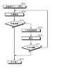
図8のフローチャートは、この発明の一実施の形態の修正処理(修正工程)の流れの一例を示している。各ステップにおいて、下記の処理がなされる。
ステップST1:外観検査装置4に対して実装済みワークが投入される。
ステップST2:外観検査装置4による外観検査がなされる。
ステップST3:はんだ付けの不良の有無が調べられる。
ステップST4:ステップST3において、はんだ付けの不良が無いと判定されると、次工程に処理が移る。
図8のフローチャートは、この発明の一実施の形態の修正処理(修正工程)の流れの一例を示している。各ステップにおいて、下記の処理がなされる。
ステップST1:外観検査装置4に対して実装済みワークが投入される。
ステップST2:外観検査装置4による外観検査がなされる。
ステップST3:はんだ付けの不良の有無が調べられる。
ステップST4:ステップST3において、はんだ付けの不良が無いと判定されると、次工程に処理が移る。
ステップST5:ステップST3において、はんだ付けの不良が有ると判定されると、不良箇所の座標が不良位置情報として記憶される。
ステップST6:不良位置情報を使用して修正装置5が不良箇所を修正する。
ステップST7:外観検査装置6によって最終的な不良の有無が判定される。不良が無いと判定されると、次工程に移る(ステップST4)。若し、不良があると判定されると、当該ワークが外観検査装置4に再度投入され、上述した処理が繰り返される。
ステップST6:不良位置情報を使用して修正装置5が不良箇所を修正する。
ステップST7:外観検査装置6によって最終的な不良の有無が判定される。不良が無いと判定されると、次工程に移る(ステップST4)。若し、不良があると判定されると、当該ワークが外観検査装置4に再度投入され、上述した処理が繰り返される。
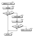
ステップST7において、不良があると判定された場合、図9に示すように、不良のあるワークをストッカーに入れて廃棄するようにしても良い。さらに、図8の処理と図9の処理とを組み合わせて、2回以上、修正しても不良が残るワークを廃棄するようにしても良い。
<2.一実施の形態>
「撮像装置及びその周辺の構成」
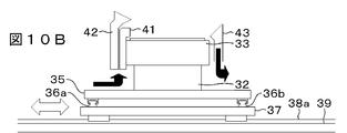
この発明は、上述したフローはんだ付けシステムにおける外観検査装置に対して適用されるものである。図10Aから図10Dは、一実施の形態の撮像装置の平面図、正面図及び一部断面図であり、図11は、撮像装置の斜視図であり、図12は、外観検査時の構成を示す正面図である。
「撮像装置及びその周辺の構成」
この発明は、上述したフローはんだ付けシステムにおける外観検査装置に対して適用されるものである。図10Aから図10Dは、一実施の形態の撮像装置の平面図、正面図及び一部断面図であり、図11は、撮像装置の斜視図であり、図12は、外観検査時の構成を示す正面図である。
撮像装置32は、産業用カメラであって筒33内に撮像素子(図示しない)及びレンズ34が設けられたものである。撮像装置32は、ワークWのはんだ付け面を下から上向きで撮像する。すなわち、はんだ付け面で上述したブリッジ等の不良が発生しているか否かが撮像装置32の撮像信号から判定される。
撮像装置32がxyステージ上に取り付けられている。xyステージは、例えばy方向の移動板35と、y方向のガイドレール36a及び36bと、x方向の移動板37と、x方向のガイドレール38a及び38bを有している。なお、xyステージの駆動源としてのステッピングモータ、位置検出用センサ等は省略されている。
撮像装置32が移動板35上に取り付けられ、移動板35の下面のスライダがガイドレール36a及び36bによって案内される。ガイドレール36a及び36bが移動板37上に平行に設けられている。移動板37の下面のスライダがガイドレール38a及び38bによって案内される。ガイドレール38a及び38bがベース板39上に平行に設けられている。撮像装置32がxyステージによってx方向及びy方向に変位自在とされている。なお、図11では、ガイドレール38a及び38b、ベース板39の図示が省略されている。
撮像装置32のレンズ34の周囲でレンズ34の前面に対してエアを吹きつけるエア吹き出し口41が設けられている。一例としてレンズ34の前面の直径以上の長さを有する直線状のエア吹き出し口41が筒33の側面に設けられている。エア吹き出し口41とレンズ34の前面を挟んで対向するエア吸い込み口43が設けられている。
図12に示すように、エア吹き出し口41から空気が吹き出されることによって形成された気流がレンズ34の前面をx方向に通ってエア吸い込み口43によって吸い込まれる。したがって、レンズ34の前面に付着している塵埃が気流によって吹き飛ばされる。エア吸い込み口43は、ダクト(図示しない)と接続されており、吸い込まれたヒューム、塵埃等がダクトを通じて作業場の外へ排気される。
さらに、他のエア吹き出し口42がエア吹き出し口41の上方に設けられている。エア吹き出し口42の吹き出し方向が斜め上方とされ、エア吹き出し口42から空気が吹き出されることによって形成された気流がワークWのはんだ付け面に向かうようになされる。はんだ付け面で反射された空気がエア吸い込み口43によって吸い込まれる。他のエア吹き出し口42からの気流によって、ワークWの周辺のヒュームが吹き飛ばされてエア吸い込み口43から外部に排気される。なお、図11では、他のエア吹き出し口42及びエア吸い込み口43の図示が省略されている。はんだ付け直後のワークWからのフラックスヒュームは、エア吹き出し口41及び42からの気流によって吹き飛ばされるのみならず、エア吸い込み口43による吸引を行うことによって、フラックスヒュームがより効果的に捕集される。
図12に示すように、ワークWは、挿入部品25d、25e、25fのそれぞれのリード26d、26e、26fが基板24のスルーホールに対して挿入され、フローはんだ付けによって、リード26d、26e、26fが基板24に対してはんだ付けされたものである。このワークWは、搬送コンベア31a及び31bによって図面と直交する方向に搬送される。外観検査装置は、箱状の筐体内に構成されており、搬送コンベア31a及び31bによって筐体内にワークWが導入され、検査を行う所定位置(検査位置と適宜称する)でワークWが静止される。ワークWは検査時に必要に応じて両側がクランプされる。検査位置において、撮像装置32がワークWのはんだ付け面を撮像し、撮像信号を解析することによってはんだ付けの良否が検査される。
二つのエア吹き出し口41及び42は、多数の小孔状の吹き出し口がy方向に直線状に配列された構成とされ、エア吹き出し口41及び42に対してエア吸い込み口43が共通に使用されている。また、エア吹き出し口41及び42は、エアの吹き出す方向が互いに違うものとされているが、空気の流れは、ほぼx方向とされている。そのため、各エア吹き出し口41及び42からの空気が干渉して流れの勢いを弱めることがない。さらに、エア吹き出し口41からの空気と、エア吹き出し口42からの空気が同一のものでもよいし、エア吹き出し口42から吹き出される空気の温度をより高くしてもよい。エア吹き出し口42から吹き出される空気の温度を高くすることによって、外観検査を終えたワークWの不良箇所を修正装置によって修正する際、ワークWのはんだ付け面のプリヒータとしても利用可能で、これによって更に確実に不良箇所の修正を行うことが可能となる。
エア吹き出し口41及び42としては、例えば図13に示すように、吹き出し口(又は吸い込み口)45及び吹き出し口46を先端に有する扇形のノズル44を使用することができる。ノズル44は、例えば樹脂又は金属からなるものである。ノズル44の基部からエア源からのエア(例えば工場エア)が導入される。エア吸い込み口43として図13と同様の形状のノズルを使用することができる。例えばエジェクターによってエアの吸い込みがなされる。
「システム構成」
図14を参照してこの発明の一実施の形態による検査装置の接続構成を説明する。撮像装置32により得られた撮像信号は、システム全体を制御するパーソナルコンピュータ51に対してアナログ方式又はデジタル方式のインターフェースを介して供給される。パーソナルコンピュータ51がxyステージ52を制御して撮像装置32のワークWに対する位置を制御する。例えばワークWを複数の領域に分割して領域毎にはんだ付けの良否が検査される。検査は、パーソナルコンピュータ51による画像処理によってなされる。得られた不良箇所の情報が次段の修正装置に対して有線又は無線で伝送される。
図14を参照してこの発明の一実施の形態による検査装置の接続構成を説明する。撮像装置32により得られた撮像信号は、システム全体を制御するパーソナルコンピュータ51に対してアナログ方式又はデジタル方式のインターフェースを介して供給される。パーソナルコンピュータ51がxyステージ52を制御して撮像装置32のワークWに対する位置を制御する。例えばワークWを複数の領域に分割して領域毎にはんだ付けの良否が検査される。検査は、パーソナルコンピュータ51による画像処理によってなされる。得られた不良箇所の情報が次段の修正装置に対して有線又は無線で伝送される。
パーソナルコンピュータ51は、エア制御部53を制御し、検査時にエア制御部53によって例えば電磁弁をONとしてエア吹き出し口41及び42から空気を吹き出させる。エア制御部53は、吸引機例えばエジェクターを制御する機能も有し、送風と平行して吸い込みがなされる。パーソナルコンピュータ51がワーク搬送部54を制御して、検査位置までワークWを搬入し、検査位置でワークWを固定し、検査終了後にワークWを搬出するようになされる。パーソナルコンピュータ51に対する入力装置55を作業者が操作して検査装置に所望の動作を行わせる。さらに、表示装置56に撮像装置32が撮像した画像、ユーザインターフェース画面等が表示される。
「検査装置の動作」
図15のフローチャートを参照してパーソナルコンピュータ51の制御によってなされる一実施の形態の動作について説明する。図示しないが、電源ON等の初期状態において、エア制御部53によって、レンズ前面及びワークのはんだ付け面に対して空気が吹きつけられ、エア吸い込み口43から空気が吸い込まれる。
ステップST11:ワークWが検査位置に搬入され、ワーク搬送部54によって検査位置に移動され、さらに、ワークWが固定される。
ステップST12:撮像装置32(図15ではカメラと表記する)が検査位置にxyステージによって移動される。
図15のフローチャートを参照してパーソナルコンピュータ51の制御によってなされる一実施の形態の動作について説明する。図示しないが、電源ON等の初期状態において、エア制御部53によって、レンズ前面及びワークのはんだ付け面に対して空気が吹きつけられ、エア吸い込み口43から空気が吸い込まれる。
ステップST11:ワークWが検査位置に搬入され、ワーク搬送部54によって検査位置に移動され、さらに、ワークWが固定される。
ステップST12:撮像装置32(図15ではカメラと表記する)が検査位置にxyステージによって移動される。
ステップST13:撮像装置32が上向き状態で対象物(ワークWのはんだ付け面)を撮像する。
ステップST14:撮像した画像がパーソナルコンピュータ51へ転送される。
ステップST15:パーソナルコンピュータ51内のソフトウェア処理によって画像が分析され、はんだ付けの良否が検査される。
ステップST16:ステップST15で得られた情報が後段の修正装置へデータ転送される。
ステップST17:ワークWが搬出される。次の検査対象のワークがある場合には、ステップST11に制御が戻る。
ステップST14:撮像した画像がパーソナルコンピュータ51へ転送される。
ステップST15:パーソナルコンピュータ51内のソフトウェア処理によって画像が分析され、はんだ付けの良否が検査される。
ステップST16:ステップST15で得られた情報が後段の修正装置へデータ転送される。
ステップST17:ワークWが搬出される。次の検査対象のワークがある場合には、ステップST11に制御が戻る。
上述した説明から分かるように、この発明の一実施の形態によれば、撮像装置の前面に塵埃が付着することを防止できると共に、付着した塵埃を吹き飛ばすことができる。また、ワークの周辺に煙のように漂っているヒュームを吹き飛ばすことができる。したがって、撮像装置の撮像画像を分析してはんだ付けの不良を検査する場合に、正常なものを不良と誤判定することを防止することができる。さらに、空気を吸引することによって、検査装置内に塵埃、ヒューム等の不要物が蓄積することを防止することができる。
<3.変形例>
以上、この発明の実施の形態について具体的に説明したが、上述の各実施の形態に限定されるものではなく、この発明の技術的思想に基づく各種の変形が可能である。また、上述の実施の形態において挙げた構成、方法、工程、形状、材料及び数値などはあくまでも例に過ぎず、必要に応じてこれと異なる構成、方法、工程、形状、材料及び数値などを用いてもよい。また、上述の実施の形態の構成、方法、工程、形状、材料及び数値などは、この発明の主旨を逸脱しない限り、互いに組み合わせることが可能である。例えば撮像装置をxyステージによって移動させているが、ワークをxy方向に移動させてもよい。また、撮像装置をx及びy方向の一方の方向に移動させ、ワークをx及びy方向の他方の方向に移動させてもよい。さらに、撮像装置に照明装置又はフラッシュ装置を設けて撮像時の照度を確保するようにしてもよい。さらに、この発明は、フローはんだ付け装置の内部のモニタに撮像装置を使用する場合に対して適用するようにしてもよい。
以上、この発明の実施の形態について具体的に説明したが、上述の各実施の形態に限定されるものではなく、この発明の技術的思想に基づく各種の変形が可能である。また、上述の実施の形態において挙げた構成、方法、工程、形状、材料及び数値などはあくまでも例に過ぎず、必要に応じてこれと異なる構成、方法、工程、形状、材料及び数値などを用いてもよい。また、上述の実施の形態の構成、方法、工程、形状、材料及び数値などは、この発明の主旨を逸脱しない限り、互いに組み合わせることが可能である。例えば撮像装置をxyステージによって移動させているが、ワークをxy方向に移動させてもよい。また、撮像装置をx及びy方向の一方の方向に移動させ、ワークをx及びy方向の他方の方向に移動させてもよい。さらに、撮像装置に照明装置又はフラッシュ装置を設けて撮像時の照度を確保するようにしてもよい。さらに、この発明は、フローはんだ付け装置の内部のモニタに撮像装置を使用する場合に対して適用するようにしてもよい。
少なくとも一つの実施形態によれば、撮像装置の前面に塵埃が付着することを防止できると共に、付着した塵埃を吹き飛ばすことができる。また、ワークの周辺に煙のように漂っているヒュームを吹き飛ばすことができる。したがって、撮像装置の撮像画像に基づいて検査する場合に、正常なものを不良と誤判定することを防止することができる。
W・・・ワーク
3・・・はんだ付け装置
4,6・・・外観検査装置
5・・・修正装置
25,25a,25b,25c・・・挿入部品
32・・・撮像装置
34・・・レンズ
36a,36b,38a,38b・・・ガイドレール
41,42・・・エア吹き出し口
43・・・エア吸い込み口
51・・・パーソナルコンピュータ
3・・・はんだ付け装置
4,6・・・外観検査装置
5・・・修正装置
25,25a,25b,25c・・・挿入部品
32・・・撮像装置
34・・・レンズ
36a,36b,38a,38b・・・ガイドレール
41,42・・・エア吹き出し口
43・・・エア吸い込み口
51・・・パーソナルコンピュータ
Claims (8)
- 撮像素子と、
撮像レンズと、
前記撮像レンズの前面を横切る気流を形成する吹き出し口とを有する
撮像装置。 - 前記気流を吸い込む吸い込み口を有する
請求項1に記載の撮像装置。 - 撮像素子と、
撮像レンズと、
前記撮像レンズの前面を横切る気流を形成する吹き出し口とを有する撮像装置を有し、
前記撮像装置の撮像信号を使用して対象物の検査を行う
検査装置。 - 部品がはんだ付けされたワークのはんだ付け面を、前記撮像装置が撮像し、
前記撮像装置の撮像信号からはんだ付け不良を検査し、
前記はんだ付けの不良箇所を記憶する
請求項3に記載の検査装置。 - 前記ワークは、フローはんだ付けによって前記基板に部品がはんだ付けされたものである
請求項4に記載の検査装置。 - 前記基板のはんだ付け面に向かう気流を形成する他の吹き出し口を有する
請求項3乃至5のいずれかに記載の検査装置。 - 前記気流を吸い込む吸い込み口を有する
請求項3乃至6のいずれかに記載の検査位置。 - 前記レンズ前面を横切る気流に比して前記基板のはんだ付け面に向かう気流の温度をより高く設定する
請求項6に記載の検査装置。
Applications Claiming Priority (2)
| Application Number | Priority Date | Filing Date | Title |
|---|---|---|---|
| JP2016072758A JP6523201B2 (ja) | 2016-03-31 | 2016-03-31 | 検査装置 |
| JP2016-072758 | 2016-03-31 |
Publications (1)
| Publication Number | Publication Date |
|---|---|
| WO2017170931A1 true WO2017170931A1 (ja) | 2017-10-05 |
Family
ID=59964753
Family Applications (1)
| Application Number | Title | Priority Date | Filing Date |
|---|---|---|---|
| PCT/JP2017/013397 Ceased WO2017170931A1 (ja) | 2016-03-31 | 2017-03-30 | 撮像装置及び検査装置 |
Country Status (2)
| Country | Link |
|---|---|
| JP (1) | JP6523201B2 (ja) |
| WO (1) | WO2017170931A1 (ja) |
Citations (5)
| Publication number | Priority date | Publication date | Assignee | Title |
|---|---|---|---|---|
| JPS61193768A (ja) * | 1985-02-22 | 1986-08-28 | Hitachi Ltd | 形状認識装置 |
| JPH0533006U (ja) * | 1991-10-07 | 1993-04-30 | 三洋電機株式会社 | 電子部品の位置検出装置 |
| JPH08166218A (ja) * | 1994-12-14 | 1996-06-25 | Omron Corp | 基板検査方法およびその装置 |
| US7138640B1 (en) * | 2002-10-17 | 2006-11-21 | Kla-Tencor Technologies, Corporation | Method and apparatus for protecting surfaces of optical components |
| JP2007093673A (ja) * | 2005-09-27 | 2007-04-12 | Seiko Epson Corp | 電気光学装置の検査装置及び検査方法 |
Family Cites Families (2)
| Publication number | Priority date | Publication date | Assignee | Title |
|---|---|---|---|---|
| JP3307777B2 (ja) * | 1994-07-07 | 2002-07-24 | 栄修 永田 | ハンダ付け方法および装置 |
| JP3287209B2 (ja) * | 1996-02-29 | 2002-06-04 | 松下電器産業株式会社 | レンズ汚れ防止装置 |
-
2016
- 2016-03-31 JP JP2016072758A patent/JP6523201B2/ja active Active
-
2017
- 2017-03-30 WO PCT/JP2017/013397 patent/WO2017170931A1/ja not_active Ceased
Patent Citations (5)
| Publication number | Priority date | Publication date | Assignee | Title |
|---|---|---|---|---|
| JPS61193768A (ja) * | 1985-02-22 | 1986-08-28 | Hitachi Ltd | 形状認識装置 |
| JPH0533006U (ja) * | 1991-10-07 | 1993-04-30 | 三洋電機株式会社 | 電子部品の位置検出装置 |
| JPH08166218A (ja) * | 1994-12-14 | 1996-06-25 | Omron Corp | 基板検査方法およびその装置 |
| US7138640B1 (en) * | 2002-10-17 | 2006-11-21 | Kla-Tencor Technologies, Corporation | Method and apparatus for protecting surfaces of optical components |
| JP2007093673A (ja) * | 2005-09-27 | 2007-04-12 | Seiko Epson Corp | 電気光学装置の検査装置及び検査方法 |
Also Published As
| Publication number | Publication date |
|---|---|
| JP6523201B2 (ja) | 2019-05-29 |
| JP2017181447A (ja) | 2017-10-05 |
Similar Documents
| Publication | Publication Date | Title |
|---|---|---|
| JP5229177B2 (ja) | 部品実装システム | |
| US8527082B2 (en) | Component mounting method, component mounting apparatus, method for determining mounting conditions, and apparatus and program for determining mounting conditions | |
| JP4767995B2 (ja) | 部品実装方法、部品実装機、実装条件決定方法、実装条件決定装置およびプログラム | |
| CN107041119B (zh) | 部件安装系统以及部件安装方法 | |
| JP6075932B2 (ja) | 基板検査管理方法および装置 | |
| KR100915128B1 (ko) | 부품장착 관리방법, 장착검사장치 및 장착시스템 | |
| JP2007287779A (ja) | 電子部品実装システムおよび搭載状態検査装置ならびに電子部品実装方法 | |
| CN102293076A (zh) | 部件组装线和部件组装方法 | |
| CN115362762B (zh) | 安装基板制造装置及安装基板制造方法 | |
| CN107443879A (zh) | 印刷装置、焊料管理系统以及焊料管理方法 | |
| JP2006202804A (ja) | 電子部品実装システムおよび電子部品搭載装置ならびに電子部品実装方法 | |
| KR20110038668A (ko) | 부품 실장 시스템 | |
| JP5144599B2 (ja) | 電子部品の装着方法 | |
| JP5927431B2 (ja) | 部品実装装置および部品実装方法 | |
| JP5927430B2 (ja) | 部品実装ライン | |
| JP7473735B2 (ja) | 異物検出装置および異物検出方法 | |
| JP5927504B2 (ja) | 部品実装システムおよび部品実装方法 | |
| JP4852456B2 (ja) | 実装ライン及び実装方法 | |
| JP2007335524A (ja) | 実装ライン | |
| JP6523201B2 (ja) | 検査装置 | |
| US20220151120A1 (en) | Correction amount calculating device and correction amount calculating method | |
| JP6742498B2 (ja) | 部品実装システムおよび部品実装方法 | |
| WO2024033961A1 (ja) | 異物検出装置および異物検出方法 | |
| JP7261309B2 (ja) | 部品実装機 | |
| WO2016075934A1 (ja) | はんだ付け修正装置およびはんだ付け修正方法 |
Legal Events
| Date | Code | Title | Description |
|---|---|---|---|
| NENP | Non-entry into the national phase |
Ref country code: DE |
|
| 121 | Ep: the epo has been informed by wipo that ep was designated in this application |
Ref document number: 17775465 Country of ref document: EP Kind code of ref document: A1 |
|
| 122 | Ep: pct application non-entry in european phase |
Ref document number: 17775465 Country of ref document: EP Kind code of ref document: A1 |