WO2017170137A1 - 光モジュール、および光モジュールの組立方法 - Google Patents
光モジュール、および光モジュールの組立方法 Download PDFInfo
- Publication number
- WO2017170137A1 WO2017170137A1 PCT/JP2017/011766 JP2017011766W WO2017170137A1 WO 2017170137 A1 WO2017170137 A1 WO 2017170137A1 JP 2017011766 W JP2017011766 W JP 2017011766W WO 2017170137 A1 WO2017170137 A1 WO 2017170137A1
- Authority
- WO
- WIPO (PCT)
- Prior art keywords
- optical
- optical component
- normal operation
- active
- prism
- Prior art date
Links
Images


Classifications
-
- G—PHYSICS
- G02—OPTICS
- G02B—OPTICAL ELEMENTS, SYSTEMS OR APPARATUS
- G02B6/00—Light guides; Structural details of arrangements comprising light guides and other optical elements, e.g. couplings
- G02B6/24—Coupling light guides
- G02B6/42—Coupling light guides with opto-electronic elements
- G02B6/4201—Packages, e.g. shape, construction, internal or external details
- G02B6/4204—Packages, e.g. shape, construction, internal or external details the coupling comprising intermediate optical elements, e.g. lenses, holograms
- G02B6/4214—Packages, e.g. shape, construction, internal or external details the coupling comprising intermediate optical elements, e.g. lenses, holograms the intermediate optical element having redirecting reflective means, e.g. mirrors, prisms for deflecting the radiation from horizontal to down- or upward direction toward a device
-
- H—ELECTRICITY
- H01—ELECTRIC ELEMENTS
- H01S—DEVICES USING THE PROCESS OF LIGHT AMPLIFICATION BY STIMULATED EMISSION OF RADIATION [LASER] TO AMPLIFY OR GENERATE LIGHT; DEVICES USING STIMULATED EMISSION OF ELECTROMAGNETIC RADIATION IN WAVE RANGES OTHER THAN OPTICAL
- H01S5/00—Semiconductor lasers
- H01S5/02—Structural details or components not essential to laser action
- H01S5/022—Mountings; Housings
- H01S5/0239—Combinations of electrical or optical elements
Definitions
- the present invention relates to an optical module and a method for assembling the optical module, and more particularly to mounting of optical components constituting the optical module.
- FIG. 9A is a cross-sectional view of the background art optical transmitter module
- FIG. 9B is another cross section of the background art optical transmitter module.
- the optical transmitter module includes the laser light source 300, the lenses 310, 311, 312, the semiconductor optical amplifier 301, and the prism 320 of FIG.
- the background art optical transmitter module further includes a prism 321, lenses 313 and 314, a modulator 330, a filter 340, and an optical attenuator 350 in FIG. 9B.
- the light 400 emitted from the laser light source 300 is converted into a collimated beam by the lens 310. Then, it is amplified by the semiconductor optical amplifier 301 via another lens 311.
- the output light from the semiconductor optical amplifier 301 is collimated again by the lens 312.
- the collimated beam is folded back by the prisms 320 and 321 to reduce the size of the module, and is focused on the modulator 330 by the lens 313.
- the optical signal modulated by the modulator 330 is collimated by the lens 314, passes through the filter 340, passes through the optical attenuator 350, and is coupled to a fiber (not shown).
- the optical transmitter module in FIG. 9 transmits the optical signal modulated by the modulator 330.
- components such as a lens and a prism are miniaturized as much as possible in order to reduce costs.
- Patent Document 1 relates to an improvement in the productivity of an optical module.
- a groove structure for alignment is provided on the substrate, and the optical axis is adjusted. It has been proposed to mount the formed lens element in a groove structure.
- optical module described above has the following problems.
- An optical module of a complicated micro-optical system has to be mounted along the order of the optical axes, and there is a problem that an optical axis cannot be formed unless an active element is driven.
- assembly must be done in order, even if it is an expensive part, the order of mounting is determined, and it may be necessary to mount in the initial stage. There is also a problem that it is big.
- An object of the present invention is to provide an optical module and an optical module assembling method capable of separately assembling optical axes of a plurality of optical components.
- an optical module according to the present invention includes an active optical component used for normal operation and an optical component that is not directly related to the active optical component and is higher or wider than the active optical component. And parts.
- the method of assembling the optical module according to the present invention is not directly related to the active optical component used for normal operation, but mounts an optical component that is higher or wider than the active optical component, and transmits the reference light as the optical component.
- the optical axis used for the normal operation is set by entering the component.
- the optical axes of a plurality of optical components can be assembled separately.
- FIG. 2A is a cross-sectional view taken along line AA of the optical transmitter module of FIG. 1
- FIG. 2B is a cross-sectional view taken along line BB of the optical transmitter module of FIG.
- FIG. 7 is a plan view showing an assembling process for explaining an assembling method of the optical transmitter module of FIG. 1.
- FIG. 10 is a plan view showing another assembling process for explaining the assembling method of the optical transmitter module of FIG. 1.
- A) is sectional drawing of the optical transmitter module of background art
- (b) is other sectional drawing of the optical transmitter module of background art.
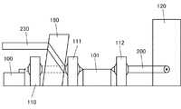
- FIG. 1 is a plan view showing an optical module according to the first embodiment of the present invention.
- 2A is a cross-sectional view taken along line AA of the optical module of FIG. 1
- FIG. 2B is a cross-sectional view taken along line BB of the optical module of FIG.
- the optical transmitter module of FIG. 1 includes a laser light source 100, a lens 110, a lens 111, a semiconductor optical amplifier (SOA) 101, a lens 112, a lens 113, a modulator 130, a lens 114, and an optical attenuator 150.
- the optical attenuator 150 is an optical attenuator composed of MEMS (Micro Electro Mechanical Systems). MEMS is a device in which component parts are integrated on a silicon substrate or a glass substrate by using a semiconductor process such as photolithography or etching.
- the optical transmitter module of FIG. 1 further includes a prism 120, a prism 121, and a filter 140.
- the semiconductor optical amplifier 101 may be referred to as an SOA 101.
- the light 200 emitted from the laser light source 100 is converted into a collimated beam by the lens 110. Then, it is amplified by the SOA 101 via another lens 111. The output light from the SOA 101 is collimated again by the lens 112. The collimated beam is folded back by the prisms 120 and 121 to reduce the size of the module, and is focused on the modulator 130 by the lens 113.
- the optical signal modulated by the modulator 130 is collimated by the lens 114, passes through the filter 140, passes through the optical attenuator 150, and is coupled to a fiber (not shown) through the lens (not shown). .
- the optical transmitter module of FIG. 1 thus transmits the optical signal modulated by the modulator 130.
- the parts that are not directly related to the active optical parts such as the prisms 120 and 121 and the filter 140 are taller than the parts directly related to the active optical parts by at least the beam diameter. That is, as shown in FIG. 2A, the prism 120 is made taller by at least the beam diameter than the component directly related to the active optical component, and its height is H1. The height H1 of the prism 120 in FIG. 2A is higher than the height H4 of the background art prism 320 in FIG. 9A. As shown in FIG. 2B, the prism 121 is made taller by at least the beam diameter than the component directly related to the active optical component, and its height is H2. The height H2 of the prism 121 of FIG.
- the filter 140 is made taller by at least the beam diameter than the component directly related to the active optical component, and its height is H3.
- the height H3 of the filter 140 in FIG. 2B is higher than the height H6 of the background-art filter 340 in FIG. 9B.
- the prisms 120 and 121 are shown as being at least as tall as the beam diameter relative to the components directly related to the active optical component, they are at least as much as the beam diameter than the components directly related to the active optical component.
- the width in the horizontal direction may be widened.
- the filter 140 is shown to be at least as tall as the beam diameter relative to the component directly related to the active optical component, but the horizontal width is at least the beam diameter relative to the component directly related to the active optical component. May be widened. It is also conceivable to use prisms 120 and 121 and a filter 140 that are wider in the horizontal direction by at least the beam diameter than components directly related to such active optical components.
- the height adjusting element 160 is inserted into the optical transmitter module shown in FIG. 1 or 2A immediately after the lens 110 as shown in FIG. 3, for example, the light 210 is transmitted to the prism 120 without passing through the SOA 101. Can be reached.
- the height adjusting element 160 is not directly related to active optical components used for normal operation, such as the laser light source 100, the SOA 101, and the modulator 130, and is an optical component that is higher or wider than the active optical components.
- the height adjustment element 160 is an optical component that is taller or wider than the component directly related to the active optical component by at least the beam diameter.
- the “height adjusting element” in this specification includes an optical component having a height higher than that of the active optical component and an optical component having a width in the horizontal direction wider than that of the active optical component.
- the height adjustment element 160 is inserted immediately after the lens 110, and the height adjustment element 161 is inserted immediately before the lens 113 as shown in FIG.
- the light 210 is folded back by the prisms 120 and 121.
- the light 220 returned by the prism 121 is condensed by the lens 113 onto the modulator 130 via the height adjustment element 160.
- the modulator 130 can be adjusted regardless of the state of the SOA 101.
- the reference light 230 is incident from a reference light source (not shown) prepared outside, and the height adjustment element 160 is inserted as appropriate, so that the laser light source 100 is not driven and other optical elements are driven. Implementation is possible.
- This optical axis adjustment is possible because all the optical axes on the way are collimated beams. Although the angle tolerance is severe with respect to the collimated beam, the translation tolerance is very loose, and even if the optical axis is translated by inserting a height adjusting element, the optical axis adjustment is hardly affected.
- the optical module of the present embodiment by inserting a height adjustment element and having an optical axis different from the optical axis when operating as a product, the optical module does not operate unless an element with large optical loss or control is performed. Even when there are elements, the optical axis can be adjusted by bypassing these elements. This not only facilitates assembly, but also greatly improves the degree of freedom in manufacturing such that an expensive element is mounted last.
- FIG. 7 is a plan view showing an assembling process for explaining an assembling method of the optical transmitter module of FIG.
- FIG. 8 is a plan view showing another assembling process for explaining the assembling method of the optical transmitter module of FIG.
- reference light 201 is incident from an external reference light source (not shown), and the prism 120 and the prism 121 are mounted on the substrate 10 at an accurate angle with respect to the reference light 201.
- the SOA 101 is mounted with reference to the reference light 201 from the outside. That is, as shown in FIG. 8, the SOA 101 is mounted at a predetermined position on the substrate 10, and the height adjusting element 162 is inserted so as to face the reference light 201.
- the position of the lens 111 is adjusted so that the reference light 201 and the SOA 101 are optically coupled with a predetermined efficiency.
- the lens 112 is adjusted so that the SOA 101 is driven and the output light 202 becomes a collimated beam.
- the lens 113, the lens 114, the modulator 130, and the optical attenuator 150 are mounted on the substrate by inserting the height adjusting element 162 in the same procedure.
- the laser light source 100 and the lens 110 are assembled.
- the laser light source 100 shown in FIGS. 1 and 2B is mounted at a predetermined position on the substrate.
- the lens 110 is aligned while shining the laser light source 100.
- an assembly can be easily assembled by connecting the ammeter to the SOA 101 and viewing the photocurrent.
- the assembly of the optical transmitter module of this embodiment is completed.
- the laser light source, the SOA, the modulator, and the optical attenuator must be mounted in this order, and the optical elements mounted in the previous process must be driven.
- the assembling method of the embodiment of the present invention the assembling may be started from any element, and it is not necessary to drive other elements.
- the optical axes of a plurality of optical parts can be separately assembled and not only the manufacturing becomes easy, but also the degree of freedom of the process of mounting an expensive part at the end increases. Therefore, it is possible to drive and assemble only the minimum necessary elements, and it is possible to minimize the discard cost due to manufacturing defects.
- the number of modulators 130 of the optical module may be two or more.
- at least one prism is a half mirror that equally divides the light 200 that is a collimated beam.
- the optical transmitter module is described as an example of the optical module.
- the present invention is not limited to this, and the present invention may be applied to an optical receiver module. It goes without saying that various modifications are possible within the scope of the invention described in the claims, and these are also included in the scope of the present invention.
- FIG. 1 An optical module including an active optical component used for normal operation and an optical component that is not directly related to the active optical component and is higher or wider than the active optical component.
- FIG. 2 The optical module according to supplementary note 1, further including a height adjusting element that is inserted into an optical axis used for normal operation and generates an optical axis different from the optical axis.
- FIG. 3 The optical module according to supplementary note 1 or supplementary note 2, wherein the height adjusting element is higher or wider than an active optical component used for normal operation.
- the optical component having a height higher or wider than the active optical component is a prism that folds the optical axis used for normal operation, 4.
- the optical component having a height higher or wider than the active optical component is a prism that folds the optical axis used for normal operation, 4.
- the optical component having a height higher or wider than the active optical component is a prism that folds the optical axis used for normal operation
- the height adjustment element includes a first height adjustment element and a second height adjustment element;
- the first height adjustment element is inserted into the optical axis opposite to the prism across an active optical component used for the normal operation, and the second height adjustment element is used for the normal operation.
- the optical module according to any one of supplementary notes 1 to 3, wherein the optical module is inserted into the optical axis between the active optical component to be used and the prism.
Landscapes
- Physics & Mathematics (AREA)
- General Physics & Mathematics (AREA)
- Optics & Photonics (AREA)
- Condensed Matter Physics & Semiconductors (AREA)
- Electromagnetism (AREA)
- Optical Couplings Of Light Guides (AREA)
- Semiconductor Lasers (AREA)
Abstract
複数の光学部品の光軸をそれぞれ分けて組み立てることを可能にする光モジュール、および光モジュールの組立方法を提供する。光モジュールは、通常動作に利用する能動光部品と、上記能動光部品に直接関係せず、上記能動光部品よりも高さが高い又は幅が広い光学部品と、を含む。
Description
本発明は、光モジュール、および光モジュールの組立方法に関し、特に光モジュールを構成する光学部品の実装に関する。
近年の注目を集めているデジタルコヒーレント通信機のように複雑な機能を実現するためには多くの機能をもつ光素子を一つのパッケージに収める必要がある。それらの光素子は、機能毎に最適な材料、構造が異なるために、モノリシック集積が難しい。そのため、異なる機能をもつ多数の光学部品を精度よく実装するマイクロオプティクスが必須となる。
このようなマイクロオプティクスを多用したモジュールは前後の部品の相対位置が重要であり、光軸の入力側から順番に組み立てなくてはならない。しかし、特に光半導体部品には動的に光を制御する部品もあり、製造時にも光素子を制御しなくてはならない。このため、製造装置に制御回路が必要になり装置が複雑化していくといった課題がある。
背景技術の光モジュールの一例として光送信機モジュールを説明する。図9(a)は背景技術の光送信機モジュールの断面図であり、図9(b)は背景技術の光送信機モジュールの他の断面図である。光送信機モジュールは、図9(a)のレーザ光源300、レンズ310、311、312、半導体光増幅器301、プリズム320を含む。背景技術の光送信機モジュールはさらに、図9(b)のプリズム321、レンズ313、314、変調器330、フィルタ340、光アッテネータ350を含む。レーザ光源300から出た光400は、レンズ310によってコリメートビームに変換される。そして別のレンズ311を経由し、半導体光増幅器301によって増幅される。この半導体光増幅器301からの出力光は、レンズ312によって再びコリメートビーム化される。コリメートビームは、モジュール小型化のためにプリズム320、321で折り返され、レンズ313で変調器330に集光される。変調器330で変調された光信号は、レンズ314でコリメート化され、フィルタ340を透過して光アッテネータ350を透過して、図示しないファイバに結合する。図9の光送信機モジュールは、変調器330で変調された光信号を送信する。図9(a)および図9(b)の背景技術の光送信機モジュールでは、レンズ、プリズムといった部品はコストを抑えるために可能な限り小型化していた。
特許文献1は、光モジュールの生産性向上に関するものであり、単一の基板上に異なる波長を用いる2つの光学素子を実装するにあたり、基板に位置合わせ用の溝構造を設け、光軸が調整されたレンズ素子を溝構造に実装することが、提案されている。
しかしながら、上述した光モジュールには以下のような課題がある。
複雑な微小光学系の光モジュールでは光軸の順番に沿って実装しなくてはならず、さらに能動素子については駆動状態にしなくては光軸ができないといった課題がある。さらに、順番に組み立てをしなくてはならないため、たとえ高価な部品であっても実装する順番が決まっており初期に実装が必要となる場合もあり、不良が出た場合のコスト損失が非常に大きいといった課題もある。
本発明の目的は、複数の光学部品の光軸をそれぞれ分けて組み立てることを可能にする光モジュール、および光モジュールの組立方法を提供することにある。
前記目的を達成するため、本発明に係る光モジュールは、通常動作に利用する能動光部品と、上記能動光部品に直接関係せず、上記能動光部品よりも高さが高い又は幅が広い光学部品と、を含む。
本発明に係る光モジュールの組立方法は、通常動作に利用する能動光部品に直接関係せず、上記能動光部品よりも高さが高い又は幅が広い光学部品を実装し、基準光を上記光学部品に入射させて、上記通常動作に利用する光軸を設定する。
本発明は、複数の光学部品の光軸をそれぞれ分けて組み立てることができる。
本発明の好ましい実施形態について、図面を参照しながら詳細に説明する。
〔第1実施形態〕
初めに、本発明の第1実施形態として光モジュールを、説明する。図1は、本発明の第1実施形態に係る光モジュールを示す平面図である。図2(a)は図1の光モジュールのA-A線に沿った断面図であり、図2(b)は図1の光モジュールのB-B線に沿った断面図である。
初めに、本発明の第1実施形態として光モジュールを、説明する。図1は、本発明の第1実施形態に係る光モジュールを示す平面図である。図2(a)は図1の光モジュールのA-A線に沿った断面図であり、図2(b)は図1の光モジュールのB-B線に沿った断面図である。
本発明の第1実施形態による光モジュールの一例として、光送信機モジュールを説明する。図1の光送信機モジュールは、レーザ光源100、レンズ110、レンズ111、半導体光増幅器(SOA:Semiconductor Optical Amplifier)101、レンズ112、レンズ113、変調器130、レンズ114、および光アッテネータ150を含む。光アッテネータ150は、MEMS(Micro Electro Mechanical Systems)で構成される光アッテネータである。MEMSとは、フォトリソグラフィーやエッチングなどの半導体プロセスを用いて、シリコン基板やガラス基板上などに要素部品を集積化したデバイスである。図1の光送信機モジュールはさらに、プリズム120、プリズム121、およびフィルタ140を含む。半導体光増幅器101を以下では、SOA101と呼ぶことがある。
レーザ光源100から出た光200は、レンズ110によってコリメートビームに変換される。そして別のレンズ111を経由し、SOA101によって増幅される。このSOA101からの出力光は、レンズ112によって再びコリメートビーム化される。コリメートビームは、モジュール小型化のためにプリズム120、121で折り返され、レンズ113で変調器130に集光される。変調器130で変調された光信号は、レンズ114でコリメート化され、フィルタ140を透過して光アッテネータ150を透過して、レンズ(図示せず)を介してファイバ(図示せず)に結合する。図1の光送信機モジュールは、変調器130で変調された光信号をこうして送信する。
図1の光送信機モジュールでは、プリズム120、121、フィルタ140といった能動光部品に直接関係しない部品は、能動光部品に直接関係する部品よりも少なくともビーム直径分だけ背を高くしてある。すなわち、図2(a)に示すようにプリズム120は、能動光部品に直接関係する部品よりも少なくともビーム直径分だけ背を高くされており、その高さはH1である。図2(a)のプリズム120の高さH1は、図9(a)の背景技術のプリズム320の高さH4より高い。図2(b)に示すようにプリズム121は、能動光部品に直接関係する部品よりも少なくともビーム直径分だけ背を高くされており、その高さはH2である。図2(b)のプリズム121の高さH2は、図9(b)の背景技術のプリズム321の高さH5より高い。図2(b)に示すようにフィルタ140は、能動光部品に直接関係する部品よりも少なくともビーム直径分だけ背を高くされており、その高さはH3である。図2(b)のフィルタ140の高さH3は、図9(b)の背景技術のフィルタ340の高さH6より高い。
なお、プリズム120、121は、能動光部品に直接関係する部品よりも少なくともビーム直径分だけ背を高くされた場合を示しているが、能動光部品に直接関係する部品よりも少なくともビーム直径分だけ水平方向の幅を広くしたものであってもよい。フィルタ140は、能動光部品に直接関係する部品よりも少なくともビーム直径分だけ背を高くされた場合を示しているが、能動光部品に直接関係する部品よりも少なくともビーム直径分だけ水平方向の幅を広くしたものであってもよい。このような能動光部品に直接関係する部品よりも、少なくともビーム直径分だけ水平方向の幅が広いプリズム120、121や、フィルタ140を用いることも考えられる。
図1や図2(a)に示される光送信器モジュールに、例えば図3に示すようにレンズ110の直後に高さ調整素子160を挿入すれば、SOA101を介さずにプリズム120まで光210を到達させることができる。高さ調整素子160は、レーザ光源100、SOA101や変調器130などの通常動作に利用する能動光部品に直接関係せず、能動光部品よりも高さが高い又は幅が広い光学部品である。高さ調整素子160は、上記能動光部品に直接関係する部品よりも少なくともビーム直径分だけ背を高く、又は幅を広くした光学部品である。以下、本明細書の「高さ調整素子」とは、能動光部品よりも高さが高い光学部品、や能動光部品よりも水平方向の幅が広い光学部品を含むものとする。
また図3に示すようにレンズ110の直後に高さ調整素子160を挿入し、図4に示すようにレンズ113の直前に高さ調整素子161を挿入することにより、高さ調整素子160からの光210はプリズム120、121で折り返される。プリズム121で折り返された光220は、高さ調整素子160を経由して、レンズ113で変調器130に集光される。このような高さ調整素子160および高さ調整素子161の挿入により、SOA101の状態とは無関係に変調器130の調整が可能となる。
或いはまた図5に示すようにレンズ112の直後に高さ調整素子161を挿入することにより、高さ調整素子160からの光210aは高さ調整素子161を経由して、プリズム120、121で折り返され、レンズ113で変調器130に集光される。このような高さ調整素子160および高さ調整素子161の挿入により、SOA101の状態とは無関係に変調器130の調整が可能となる。
さらに図6に示すように外部に用意した基準光源(図示せず)から基準光230を入射し、適宜高さ調整素子160を挿入することでレーザ光源100も駆動させずに他の光素子の実装が可能となる。
このような光軸調整が可能となるのは、途中の光軸がすべてコリメートビームになっているためである。コリメートビームに対して角度トレランスは厳しいが、平行移動トレランスは非常にゆるく、高さ調整素子を挿入することで光軸が平行移動しても光軸調整にはほとんど影響を与えない。
本実施形態の光モジュールによれば、高さ調整素子を挿入して、製品として動作させる場合の光軸と異なる光軸を持たせることにより、光損失の大きな素子や制御を行わなければ動作しない素子がある場合でも、それらの素子を迂回して光軸調整が可能となる。これにより組み立てが容易になるだけではなく、高価な素子を最後に搭載するといった製造上の自由度が格段に向上する。
〔第2実施形態〕
次に、本発明の第2実施形態として光モジュールの組立方法を、説明する。光モジュールの組立方法の一例として、光送信機モジュールの組立方法を説明する。図7は、図1の光送信機モジュールの組立方法を説明するための、ある組立過程を示す平面図である。図8は、図1の光送信機モジュールの組立方法を説明するための、他の組立過程を示す平面図である。
次に、本発明の第2実施形態として光モジュールの組立方法を、説明する。光モジュールの組立方法の一例として、光送信機モジュールの組立方法を説明する。図7は、図1の光送信機モジュールの組立方法を説明するための、ある組立過程を示す平面図である。図8は、図1の光送信機モジュールの組立方法を説明するための、他の組立過程を示す平面図である。
(本実施形態の組み立て)
光送信器モジュールを組み立てるための基板10には、各素子を搭載するためのマーカ(図示せず)や電極(図示せず)が予め形成されている。
光送信器モジュールを組み立てるための基板10には、各素子を搭載するためのマーカ(図示せず)や電極(図示せず)が予め形成されている。
まず図7に示すように外部の基準光源(図示せず)から基準光201を入射させ、プリズム120およびプリズム121を基準光201に対して正確な角度で基板10に実装する。次に外部からの基準光201を参照してSOA101を搭載する。すなわち、図8に示すようにSOA101を基板10の所定の位置に実装し、高さ調整素子162を基準光201に正対するように挿入する。基準光201とSOA101が所定の効率で光結合するように、レンズ111の位置を調整する。最後に、SOA101を駆動して出力光202がコリメートビームになるように、レンズ112を調整する。
図1や図2(b)に示される、レンズ113、レンズ114、変調器130および光アッテネータ150も同様の手順で高さ調整素子162を挿入して、基板に実装していく。そして最後にレーザ光源100とレンズ110を組み立てていく。図1や図2(b)に示される、レーザ光源100は基板上の所定の位置に搭載する。次にレーザ光源100を光らせながらレンズ110を調芯するが、この時SOA101に電流計をつないで光電流を見ることで容易に組み立てが可能である。こうして、本実施形態の光送信機モジュールの組立てが完成する。
背景技術の工程ではレーザ光源、SOA、変調器、光アッテネータと順番に実装し、かつそれぞれ前工程で搭載した光素子を駆動しなければならない。これに対し、本発明の実施形態の組立方法では、どの素子から組み立てを開始しても良く、他の素子を駆動する必要も無くなる。
本実施形態によれば、複数の光部品の光軸をそれぞれ分けて組み立てることが可能となり製造が容易になるだけではなく、高価な部品を最後に搭載するといった工程の自由度が高くなる。そのため、必要最小限の素子だけ駆動して組み立てが可能となり、さらに製造不良による破棄コストを最小に抑えることができるようになる。
以上、本発明の好ましい実施形態を説明したが、本発明はこれに限定されるものではない。例えば、例えば光モジュールの変調器130は2つ以上でも良く、その場合には少なくとも一つのプリズムはコリメートビームである光200を等分に分岐するハーフミラーとなる。上述した実施形態では光モジュールとして光送信機モジュールを例に説明したが、これに限られず、光受信機モジュールに本発明を適用してもよい。請求の範囲に記載した発明の範囲内で、種々の変形が可能であり、それらも本発明の範囲に含まれることはいうまでもない。
上記の実施形態の一部又は全部は、以下の付記のようにも記載されうるが、以下には限られない。
(付記1)通常動作に利用する能動光部品と、前記能動光部品に直接関係せず、前記能動光部品よりも高さが高い又は幅が広い光学部品と、を含む光モジュール。
(付記2)通常動作に利用する光軸に挿入され、前記光軸とは異なる光軸を生成する高さ調整素子をさらに含む、付記1に記載の光モジュール。
(付記3)前記高さ調整素子は、通常動作に利用する能動光部品よりも高さが高い又は幅が広い、付記1又は付記2に記載の光モジュール。
(付記4)前記能動光部品よりも高さが高い又は幅が広い光学部品は、通常動作に利用する光軸を折り返すプリズムであり、
前記高さ調整素子は、前記通常動作に利用する能動光部品を挟んで前記プリズムとは反対側の前記光軸に挿入される、付記1乃至付記3のいずれか一つに記載の光モジュール。
(付記5)前記能動光部品よりも高さが高い又は幅が広い光学部品は、通常動作に利用する光軸を折り返すプリズムであり、
前記高さ調整素子は、前記通常動作に利用する能動光部品と前記プリズムとの間の前記光軸に挿入される、付記1乃至付記3のいずれか一つに記載の光モジュール。
(付記6)前記能動光部品よりも高さが高い又は幅が広い光学部品は、通常動作に利用する光軸を折り返すプリズムであり、
前記高さ調整素子は第1の高さ調整素子と第2の高さ調整素子とを含み、
前記第1の高さ調整素子は、前記通常動作に利用する能動光部品を挟んで前記プリズムとは反対側の前記光軸に挿入され、前記第2の高さ調整素子は、前記通常動作に利用する能動光部品と前記プリズムとの間の前記光軸に挿入される、付記1乃至付記3のいずれか一つに記載の光モジュール。
(付記7)前記高さ調整素子は、プリズムまたはフィルタである、付記1乃至付記6のいずれか一つに記載の光モジュール。
(付記8)通常動作に利用する能動光部品に直接関係せず、前記能動光部品よりも高さが高い又は幅が広い光学部品を実装し、基準光を前記光学部品に入射させて、前記通常動作に利用する光軸を設定する、光モジュールの組立方法。
(付記9)通常動作に利用する光軸に高さ調整素子を挿入して、前記通常動作に利用する光軸とは異なる光軸を生成する、付記8に記載の光モジュールの組立方法。
(付記10)前記高さ調整素子を挿入した後に、前記通常動作に利用する能動光部品を実装する、付記9に記載の光モジュールの組立方法。
(付記11)基準光を入射させて、前記基準光を折り返すように一対のプリズムを実装した後、前記高さ調整素子を挿入する、付記9又は付記10に記載の光モジュールの組立方法。
以上、上述した実施形態を模範的な例として本発明を説明した。しかしながら、本発明は、上述した実施形態には限定されない。即ち、本発明は、本発明のスコープ内において、当業者が理解し得る様々な態様を適用することができる。
この出願は、2016年3月31日に出願された日本出願特願2016-71790号を基礎とする優先権を主張し、その開示の全てをここに取り込む。
100 レーザ光源
110、111、112、113、114 レンズ
101 半導体光増幅器
120、121 プリズム
130 変調器
140 フィルタ
150 光アッテネータ
160 高さ調整素子
161 高さ調整素子
162 高さ調整素子
200、210、210a、220 光
201 基準光
202 出力光
110、111、112、113、114 レンズ
101 半導体光増幅器
120、121 プリズム
130 変調器
140 フィルタ
150 光アッテネータ
160 高さ調整素子
161 高さ調整素子
162 高さ調整素子
200、210、210a、220 光
201 基準光
202 出力光
Claims (11)
- 通常動作に利用する能動光部品と、前記能動光部品に直接関係せず、前記能動光部品よりも高さが高い又は幅が広い光学部品と、を含む光モジュール。
- 通常動作に利用する光軸に挿入され、前記光軸とは異なる光軸を生成する高さ調整素子をさらに含む、請求項1に記載の光モジュール。
- 前記高さ調整素子は、通常動作に利用する能動光部品よりも高さが高い又は幅が広い、請求項1又は請求項2に記載の光モジュール。
- 前記能動光部品よりも高さが高い又は幅が広い光学部品は、通常動作に利用する光軸を折り返すプリズムであり、
前記高さ調整素子は、前記通常動作に利用する能動光部品を挟んで前記プリズムとは反対側の前記光軸に挿入される、請求項1乃至請求項3のいずれか一項に記載の光モジュール。 - 前記能動光部品よりも高さが高い又は幅が広い光学部品は、通常動作に利用する光軸を折り返すプリズムであり、
前記高さ調整素子は、前記通常動作に利用する能動光部品と前記プリズムとの間の前記光軸に挿入される、請求項1乃至請求項3のいずれか一項に記載の光モジュール。 - 前記能動光部品よりも高さが高い又は幅が広い光学部品は、通常動作に利用する光軸を折り返すプリズムであり、
前記高さ調整素子は第1の高さ調整素子と第2の高さ調整素子とを含み、
前記第1の高さ調整素子は、前記通常動作に利用する能動光部品を挟んで前記プリズムとは反対側の前記光軸に挿入され、前記第2の高さ調整素子は、前記通常動作に利用する能動光部品と前記プリズムとの間の前記光軸に挿入される、請求項1乃至請求項3のいずれか一項に記載の光モジュール。 - 前記高さ調整素子は、プリズムまたはフィルタである、請求項1乃至請求項6のいずれか一項に記載の光モジュール。
- 通常動作に利用する能動光部品に直接関係せず、前記能動光部品よりも高さが高い又は幅が広い光学部品を実装し、基準光を前記光学部品に入射させて、前記通常動作に利用する光軸を設定する、光モジュールの組立方法。
- 通常動作に利用する光軸に高さ調整素子を挿入して、前記通常動作に利用する光軸とは異なる光軸を生成する、請求項8に記載の光モジュールの組立方法。
- 前記高さ調整素子を挿入した後に、前記通常動作に利用する能動光部品を実装する、請求項9に記載の光モジュールの組立方法。
- 基準光を入射させて、前記基準光を折り返すように一対のプリズムを実装した後、前記高さ調整素子を挿入する、請求項9又は請求項10に記載の光モジュールの組立方法。
Applications Claiming Priority (2)
| Application Number | Priority Date | Filing Date | Title |
|---|---|---|---|
| JP2016-071790 | 2016-03-31 | ||
| JP2016071790 | 2016-03-31 |
Publications (1)
| Publication Number | Publication Date |
|---|---|
| WO2017170137A1 true WO2017170137A1 (ja) | 2017-10-05 |
Family
ID=59964502
Family Applications (1)
| Application Number | Title | Priority Date | Filing Date |
|---|---|---|---|
| PCT/JP2017/011766 WO2017170137A1 (ja) | 2016-03-31 | 2017-03-23 | 光モジュール、および光モジュールの組立方法 |
Country Status (1)
| Country | Link |
|---|---|
| WO (1) | WO2017170137A1 (ja) |
Citations (6)
| Publication number | Priority date | Publication date | Assignee | Title |
|---|---|---|---|---|
| JP2006154535A (ja) * | 2004-11-30 | 2006-06-15 | Oki Electric Ind Co Ltd | 光モジュール |
| JP2006350047A (ja) * | 2005-06-17 | 2006-12-28 | Matsushita Electric Ind Co Ltd | 導波路素子の光結合モジュールおよびその光軸調整方法 |
| WO2007032182A1 (ja) * | 2005-09-13 | 2007-03-22 | Nec Corporation | 光送信モジュールおよびその製造方法 |
| JP2009260182A (ja) * | 2008-04-21 | 2009-11-05 | Mitsubishi Electric Corp | 波長ロッカモジュール |
| JP2013148825A (ja) * | 2012-01-23 | 2013-08-01 | Japan Oclaro Inc | 光モジュール |
| JP2014149494A (ja) * | 2013-02-04 | 2014-08-21 | Sumitomo Electric Ind Ltd | 光送信モジュールの製造方法 |
-
2017
- 2017-03-23 WO PCT/JP2017/011766 patent/WO2017170137A1/ja active Application Filing
Patent Citations (6)
| Publication number | Priority date | Publication date | Assignee | Title |
|---|---|---|---|---|
| JP2006154535A (ja) * | 2004-11-30 | 2006-06-15 | Oki Electric Ind Co Ltd | 光モジュール |
| JP2006350047A (ja) * | 2005-06-17 | 2006-12-28 | Matsushita Electric Ind Co Ltd | 導波路素子の光結合モジュールおよびその光軸調整方法 |
| WO2007032182A1 (ja) * | 2005-09-13 | 2007-03-22 | Nec Corporation | 光送信モジュールおよびその製造方法 |
| JP2009260182A (ja) * | 2008-04-21 | 2009-11-05 | Mitsubishi Electric Corp | 波長ロッカモジュール |
| JP2013148825A (ja) * | 2012-01-23 | 2013-08-01 | Japan Oclaro Inc | 光モジュール |
| JP2014149494A (ja) * | 2013-02-04 | 2014-08-21 | Sumitomo Electric Ind Ltd | 光送信モジュールの製造方法 |
Similar Documents
| Publication | Publication Date | Title |
|---|---|---|
| US10598873B2 (en) | Optical alignment of an optical subassembly to an optoelectronic device | |
| JP6340902B2 (ja) | 光モジュールの製造方法 | |
| US8267532B2 (en) | Passive alignment method and its application in micro projection devices | |
| JP7040548B2 (ja) | 多チャネル発光モジュールの製造方法、及び多チャネル発光モジュール | |
| US7982957B2 (en) | Optical apparatus using a lens array | |
| JP6647375B2 (ja) | 光合波器の製造装置 | |
| US10499023B2 (en) | Projection device and a method of manufacturing a projection device | |
| CN104297856B (zh) | 波长选择开关及其制造方法 | |
| JP6230720B2 (ja) | 光部品、光モジュールおよび光部品の製造方法 | |
| Murao et al. | Integrated Spatial Optical System for Compact 28-Gb/s\(\times\) 4-lane Transmitter Optical Subassemblies | |
| JP2007010854A (ja) | 光軸補正用平行平板を用いた光通信用モジュールとその製造方法 | |
| WO2017170137A1 (ja) | 光モジュール、および光モジュールの組立方法 | |
| WO2014045340A1 (ja) | 光学素子、光源ユニット及びヘッドアップディスプレイ | |
| WO2018128118A1 (ja) | 光通信装置 | |
| US6816323B2 (en) | Coupling with strong lens and weak lens on flexure | |
| JPH1168243A (ja) | 光モジュール及び光軸調整方法 | |
| JP6566022B2 (ja) | 集積プリズム及び集積プリズムの構成方法 | |
| JP2009192971A (ja) | プロジェクタ、及び調整方法 | |
| WO2014045341A1 (ja) | 光学素子、光源ユニット及びヘッドアップディスプレイ | |
| US9081201B2 (en) | Optical unit and wavelength selective switch | |
| US6703605B2 (en) | Optoelectronic micromodule | |
| US20180259714A1 (en) | Optical dichroic element and optical dichroic module | |
| JP2003156664A (ja) | 光伝送モジュール | |
| JPH09113769A (ja) | 光学デバイス | |
| WO2015040953A1 (ja) | 光送信モジュールおよび光送信モジュールの組立方法 |
Legal Events
| Date | Code | Title | Description |
|---|---|---|---|
| NENP | Non-entry into the national phase |
Ref country code: DE |
|
| 121 | Ep: the epo has been informed by wipo that ep was designated in this application |
Ref document number: 17774675 Country of ref document: EP Kind code of ref document: A1 |
|
| 122 | Ep: pct application non-entry in european phase |
Ref document number: 17774675 Country of ref document: EP Kind code of ref document: A1 |
|
| NENP | Non-entry into the national phase |
Ref country code: JP |