WO2017169761A1 - 配線基板およびこれを備えるプローブカード - Google Patents
配線基板およびこれを備えるプローブカード Download PDFInfo
- Publication number
- WO2017169761A1 WO2017169761A1 PCT/JP2017/010317 JP2017010317W WO2017169761A1 WO 2017169761 A1 WO2017169761 A1 WO 2017169761A1 JP 2017010317 W JP2017010317 W JP 2017010317W WO 2017169761 A1 WO2017169761 A1 WO 2017169761A1
- Authority
- WO
- WIPO (PCT)
- Prior art keywords
- plating layer
- plating
- electrode
- wiring board
- film
- Prior art date
- Legal status (The legal status is an assumption and is not a legal conclusion. Google has not performed a legal analysis and makes no representation as to the accuracy of the status listed.)
- Ceased
Links
Images



Classifications
-
- G—PHYSICS
- G01—MEASURING; TESTING
- G01R—MEASURING ELECTRIC VARIABLES; MEASURING MAGNETIC VARIABLES
- G01R1/00—Details of instruments or arrangements of the types included in groups G01R5/00 - G01R13/00 and G01R31/00
- G01R1/02—General constructional details
- G01R1/06—Measuring leads; Measuring probes
- G01R1/067—Measuring probes
- G01R1/073—Multiple probes
-
- H—ELECTRICITY
- H05—ELECTRIC TECHNIQUES NOT OTHERWISE PROVIDED FOR
- H05K—PRINTED CIRCUITS; CASINGS OR CONSTRUCTIONAL DETAILS OF ELECTRIC APPARATUS; MANUFACTURE OF ASSEMBLAGES OF ELECTRICAL COMPONENTS
- H05K1/00—Printed circuits
- H05K1/02—Details
-
- H—ELECTRICITY
- H05—ELECTRIC TECHNIQUES NOT OTHERWISE PROVIDED FOR
- H05K—PRINTED CIRCUITS; CASINGS OR CONSTRUCTIONAL DETAILS OF ELECTRIC APPARATUS; MANUFACTURE OF ASSEMBLAGES OF ELECTRICAL COMPONENTS
- H05K3/00—Apparatus or processes for manufacturing printed circuits
- H05K3/22—Secondary treatment of printed circuits
- H05K3/24—Reinforcing of the conductive pattern
Definitions
- the present invention relates to a wiring board having electrodes formed on the main surface and a probe card including the wiring board.
- the multilayer wiring substrate 100 described in Patent Document 1 includes a core substrate 101 formed by stacking a plurality of ceramic layers 101 a and a plurality of resin layers 102 a (for example, polyimide).
- the resin part 102 which comprises.
- a plurality of connection electrodes 103 connected to the probe pins are formed on the upper surface of the multilayer wiring substrate 100.
- a plurality of external electrodes 104 provided so as to correspond to the connection electrodes 103 are arranged on the lower surface of the multilayer wiring substrate 100 at a pitch wider than the pitch of the connection electrodes 103.
- connection electrode 103 and the external electrode 104 are connected to each other via the wiring electrode 105 and the interlayer connection conductor 106 formed inside the multilayer wiring substrate 100, so that a rewiring structure is formed on the multilayer wiring substrate 100. Is formed.
- the connection electrode 103 to which the probe pin is connected is composed of, for example, a plurality of plating layers laminated in the order of Cu plating, Ni plating, and Au plating. There is.
- the connection electrode 103 since the probe pin is contacted many times, the connection electrode 103 is likely to be worn, and it is necessary to increase the thickness of the Au plating layer as the outermost layer so that it can withstand long-term use.
- the Au plating layer is formed on the outermost layer to prevent corrosion.
- a measuring method using a fluorescent X-ray film thickness meter as a film thickness measuring method for confirming whether each plating layer is formed with a predetermined film thickness.
- a fluorescent X-ray film thickness meter is used, the thickness of each plating layer of the connection electrode 103 can be measured non-destructively by irradiating the connection electrode 103 with fluorescent X-rays after the connection electrode 103 is formed.
- the intensity of the fluorescent X-rays is greatly attenuated, so the thickness of the Cu plating layer and the Ni plating layer on the inner layer side can be accurately determined. There is a problem that accurate measurement is not possible.
- the present invention has been made in view of the above problems, and in a wiring board having electrodes formed of a plurality of plating layers, the thickness of each plating layer is measured nondestructively with a fluorescent X-ray film thickness meter.
- the purpose is to improve measurement accuracy.
- the multilayer wiring board of the present invention is a wiring board in which an electrode is formed on a main surface, the electrode is formed of a plurality of plating layers having an Au plating layer as an outermost layer, and the Au It is characterized in that a concave portion is formed in the plating layer.
- the inner layer side plating layer can be measured using a fluorescent X-ray film thickness meter.
- the measurement accuracy when measuring the film thickness can be improved.
- the electrode itself can be used as a recognition mark by an image by utilizing the difference in contrast between the recess and its surroundings, accurate position coordinates can be recognized even when the electrode shape is distorted. .
- the concave portion may be a through-hole penetrating the Au plating layer.
- a through-hole is formed in the thick Au plating layer, by plating with fluorescent X-rays from this through-hole, plating on the electrode inner layer side using a fluorescent X-ray film thickness meter The measurement accuracy when measuring the thickness of the layer can be improved.
- the bottom of the recess may be covered with an Au film having a film quality different from that of the Au plating layer.
- an Au film having a film quality different from that of the Au plating layer at the bottom of the through hole of the recess the difference in contrast between the recess and the surrounding area is used to recognize when the electrode is used as a recognition mark. The accuracy can be further improved.
- an Au film on the bottom of the recess corrosion of the plating layer on the electrode inner layer side can be prevented, and durability can be improved.
- the Au coating may further cover the side surface of the recess and the surface of the electrode. In this case, since the durability of the electrode is increased by forming the Au film on the electrode surface, long-term reliability is improved.
- the Au film in the concave portion may have a thickness of 1 ⁇ m or less.
- the film thickness of the Au film is 1 ⁇ m or less, the measurement error using the fluorescent X-ray film thickness meter is small, so the accuracy of the film thickness measurement using the fluorescent X-ray film thickness meter can be improved.
- the above wiring board for a probe card for performing an electrical inspection of an object to be inspected.
- a probe card for performing an electrical inspection of an object to be inspected.
- the fluorescence generated due to the thickness of the Au plating layer by providing the recess in the Au plating layer that is the outermost layer of the electrode composed of a plurality of plating layers formed on the main surface of the wiring board. Since the error of the film thickness measurement by the X-ray film thickness meter can be reduced, the accuracy of the film thickness measurement of each plating layer by nondestructive can be improved. Further, the electrode can be used as a recognition mark by utilizing the difference in contrast between the concave portion and the periphery thereof on the electrode surface.
- FIGS. 1 and 3 A wiring board 1 according to a first embodiment of the present invention will be described with reference to FIGS. 1 and 3.
- 1 is an enlarged view of a cross section of the wiring board 1
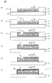
- FIG. 3 is a view showing a method for manufacturing the wiring board 1 of FIG.
- a wiring board 1 has a plurality of electrodes 3 formed on a main surface 2a of a core board 2, and is used by being mounted on a probe card used for electrical inspection of non-inspected objects such as semiconductor elements, for example.
- the wiring substrate 1 includes a core substrate 2 and electrodes 3 formed on the main surface 2 a of the core substrate 2.
- a power feeding film 4 is formed between the core substrate 2 and the electrode 3.
- a plurality of electrodes are usually formed on the wiring board 1 mounted on the probe card, and a description will be given with reference to an enlarged view of one of the electrodes.
- the core substrate 2 may be formed of various ceramics such as a low-temperature co-fired ceramic (LTCC) or a high-temperature fired ceramic (HTCC) mainly composed of a ceramic (for example, alumina) containing borosilicate glass. it can.
- the core substrate 2 may have a multilayer structure.
- a power feeding film 4 is formed on the main surface 2 a of the core substrate 2. This is for supplying power when performing electroplating, and a metal film such as Ti or Cu is formed by sputtering. Further, an electrode 3 made of a plurality of plating layers is formed on the power feeding film 4.
- the electrode 3 includes a Cu plating layer 3a, a Ni plating layer 3b, an Au plating layer 3c, and an Au coating 3d that covers the surface of the electrode 3.
- the Cu plating layer 3a and the Ni plating layer 3b are formed by electrolytic Cu plating and electrolytic Ni plating, respectively.
- the Au plating layer 3c is formed by, for example, electrolytic Au plating for plating hard Au, and has a thickness of about 2 ⁇ m.
- the Cu plating layer 3a or Ni plating layer is used. It is formed thicker than 3b.
- the recessed part 5 is formed in Au plating layer 3c. In this embodiment, the recess 5 is a through-hole penetrating the Au plating layer 3c, but the recess 5 may not penetrate the Au plating layer 3c.
- the Au coating 3d is formed by soft Au plating having a film quality different from that of the Au plating layer 3c.
- it can be formed by electroless plating (substitution electroless plating or substitution reduction electroless plating), electrolytic plating, electrolytic plating (partial plating) by brush plating for repair, or the like.
- the Au coating 3 d is formed so as to cover the bottom and side surfaces of the recess 5 and the surface of the electrode 3.
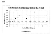
- FIG. 2 shows how much the actual thickness measurement value of the Ni plating layer 3b on the inner layer side of the electrode 3 and the measurement value by fluorescent X-rays depend on the thickness of the outermost Au plating layer 3c of the electrode 3. It is the graph which showed whether the difference
- the horizontal axis represents the film thickness of the Au plating layer 3c
- the vertical axis represents the error between the actual measured value of the Ni plated layer 3b and the measured value by fluorescent X-ray (the actual measured thickness value is subtracted from the measured fluorescent X-ray value). Calculated).
- the thickness of the Au plating layer 3c which is the outermost layer, exceeds 1 ⁇ m, the error between the actual thickness measurement value of the Ni plating layer 3b and the measurement value by fluorescent X-rays tends to increase. I understand.
- X-rays are irradiated through the Au coating 3d formed so as to cover the bottom of the recess 5, and the film thicknesses of the Cu plating layer 3a and the Ni plating layer 3b on the inner layer side are measured. If the Au film 3d is formed so that the film thickness of the Au film 3d is 1 ⁇ m or less, in particular, the error between the actual thickness measurement value and the measurement value by fluorescent X-rays can be reduced.
- the core substrate 2 is prepared, and the power supply film 4 is formed on the main surface 2 a of the core substrate 2.
- the power supply film 4 is formed by forming a metal film such as Ti or Cu by sputtering.
- a plating resist 6 is formed on the power supply film 4.
- the plating resist 6 can be formed, for example, by applying a photosensitive resin such as an epoxy resin at a predetermined position, exposing and developing.
- the Cu plating layer 3a and the Ni plating layer 3b of the electrode 3 are laminated and formed by electrolytic Cu plating and electrolytic Ni plating, respectively.
- an Au plating resist 7 is additionally formed at a predetermined position of the Ni plating layer 3b (a position where the concave portion of the Au plating layer 3c is formed).
- the Au plating resist 7 can also be formed of a photosensitive resin such as an epoxy resin in the same manner as the plating resist 6.
- a hard Au Au plating layer 3c is formed on the surface of the Ni plating layer 3b by electrolytic Au plating. Thereafter, as shown in FIG. 3D, the plating resist 6 and the Au plating resist 7 are peeled off to form the recess 5 in the Au plating layer 3c.
- the region covered with the plating resist 6 of the power feeding film 4, that is, the power feeding film 4 exposed from the electrode 3 is removed by etching.
- the Au coating 3d is formed to a thickness of 1 ⁇ m or less by performing electroless plating of, for example, soft Au having a film quality different from that of the Au plating layer 3c on the bottom and side surfaces of the recess 5 and the surface of the electrode 3. Thereby, the wiring board 1 is completed.
- the thickness of each of the plating layers 3a to 3c is measured nondestructively using a fluorescent X-ray film thickness meter. Since X-rays can be irradiated through the Au coating 3d having a thickness of 1 ⁇ m or less that covers the bottom of the concave portion 5 that is thinner than the Au plating layer 3c, fluorescent X-rays generated by passing through the thick Au plating layer 3c are used. Can be significantly suppressed, and the film thicknesses of the Cu plating layer 3a and the Ni plating layer 3b on the inner layer side of the electrode 3 can be accurately measured without destruction.
- the concave portion 5 can be used as a recognition mark. That is, since a recognition mark can be formed on each electrode, for example, alignment of probe pins can be easily performed.
- the durability of the electrode 3 is increased, and the long-term reliability of the wiring board 1 can be improved. Furthermore, by setting the thickness of the Au coating 3d to 1 ⁇ m or less, it is possible to improve the accuracy of film thickness measurement by the fluorescent X-ray film thickness meter of the Cu plating layer 3a on the inner layer side of the electrode 3 and the Ni plating layer 3b.
- the Au coating 3 d may cover only the bottom of the recess 5. In this case, since the film quality of the Au plating is different between the recess 5 and the periphery thereof, the contrast difference can be increased, and the electrode 3 can be easily used as a recognition mark.
- FIG. 5 is a diagram showing a method for manufacturing the wiring board 1.
- the difference between the wiring board 1 according to this embodiment and the first embodiment described with reference to FIGS. 1 and 3 is that the manufacturing method of the wiring board 1 is different. Since other configurations are the same as those of the wiring substrate 1 of the first embodiment, the description thereof is omitted by giving the same reference numerals.
- the core substrate 2 is prepared, and the power supply film 4 is formed on the main surface 2a.
- the power supply film 4 is formed by forming a metal film such as Ti or Cu by sputtering.
- a plating resist 6 is formed on the power supply film 4.
- the plating resist 6 can be formed, for example, by applying a photosensitive resin such as an epoxy resin at a predetermined position, exposing and developing.
- the Cu plating layer 3a, the Ni plating layer 3b, and the Au plating layer 3c of the electrode 3 are formed by electrolytic Cu plating, electrolytic Ni plating, and electrolytic Au plating (hard Au plating), respectively.
- the plating resist 6 is peeled off, and the region of the power feeding film 4 covered with the plating resist 6, that is, the power feeding film 4 exposed from the electrode 3 is removed by etching.
- a portion where the concave portion 5 is formed on the surface of the Au plating layer 3c is cut out with a probe having a sharp tip to form the concave portion 5.
- the hardness of the Ni plating layer 3b is higher than that of the Au plating layer 3c, the Ni plating layer 3b is exposed from the bottom of the recess 5 without being pulled out even if the probe hits the Ni plating layer 3b.
- an Au coating 3d is formed on the bottom and side surfaces of the recess 5 and the surface of the electrode 3 by partial electrolytic plating (brush plating), and the wiring substrate 1 is completed.
- the Au coating 3d is formed by soft Au plating having a film quality different from that of the Au plating layer 3c.
- the present invention is not limited to the above-described embodiment, and various modifications other than those described above can be made without departing from the spirit of the present invention.
- the Au coating 3d is formed by soft Au plating has been described.
- the Au plating layer 3c may be different from the film quality, and is not limited to soft Au plating.
- the present invention is not limited to the above-described probe card wiring substrate, but can be applied to various wiring substrates having electrodes formed on the surface thereof.
Landscapes
- Engineering & Computer Science (AREA)
- Microelectronics & Electronic Packaging (AREA)
- Manufacturing & Machinery (AREA)
- Physics & Mathematics (AREA)
- General Physics & Mathematics (AREA)
- Measuring Leads Or Probes (AREA)
- Structure Of Printed Boards (AREA)
- Analysing Materials By The Use Of Radiation (AREA)
Abstract
複数のめっき層からなる電極を有する配線基板において、電極の各めっき層の膜厚を、蛍光X線膜厚計を使用して非破壊で測定する際に、測定精度を向上させる。 配線基板1は、コア基板2の主面2aに電極3が形成されてなる。電極3はCuめっき層3a、Niめっき層3b、Auめっき層3cが順次積層されて形成され、Auめっき層3cに凹部5が形成されている。凹部5の底部と側面、および電極3の表面は、Auめっき層3cとは膜質の異なるAuめっきで形成されたAu皮膜3dで被覆されている。凹部5の底部からX線を照射することで、電極3の内層側のCuめっき層3a、Niめっき層3cの膜厚の測定精度を向上することができる。
Description
本発明は、主面に電極が形成された配線基板およびこれを備えるプローブカードに関する。
近年の半導体素子の外部端子の高密度化に伴い、この種の半導体素子の電気検査が可能なプローブカード用の配線基板の開発が進められている。例えば、図6に示すように、特許文献1に記載の積層配線基板100は、複数のセラミック層101aが積層されて成るコア基板101と、複数の樹脂層102a(例えば、ポリイミド)が積層されて成る樹脂部102とを備える。ここで、積層配線基板100の上面には、それぞれプローブピンと接続される複数の接続電極103が形成される。また、積層配線基板100の下面には、各接続電極103それぞれに対応するように設けられた複数の外部電極104が、各接続電極103のピッチよりも広いピッチで配置される。そして、対応する接続電極103と外部電極104同士が、積層配線基板100の内部に形成された配線電極105および層間接続導体106を介して接続されることで、積層配線基板100に再配線構造が形成されている。
このようなプローブカードに搭載される積層配線基板100では、プローブピンが接続される接続電極103は、例えば、Cuめっき、Niめっき、Auめっきの順に積層された複数のめっき層から構成される場合がある。この場合、何度もプローブピンを接触させるため接続電極103が摩耗しやすくなり、最外層となるAuめっき層の厚みを増して、長期の使用に耐えられるようにする必要がある。また、接続電極103の内層のCuやNiのめっき層は腐食しやすいため、最外層にAuめっき層を形成することで、腐食を防止する役割もある。
ところで、各めっき層が所定の膜厚で形成されているかを確認するための膜厚測定方法に、蛍光X線膜厚計を使用した測定方法がある。蛍光X線膜厚計を使用すると、接続電極103を形成した後、接続電極103に蛍光X線を照射することにより非破壊で接続電極103の各めっき層の膜厚を測定することができる。しかしながら、接続電極103のように、最外層のAuめっき層が厚く形成されている場合、蛍光X線の強度が大きく減衰されるため、内層側のCuめっき層やNiめっき層の膜厚の正確な測定ができないという問題がある。
本発明は、上記した課題に鑑みてなされたものであり、複数のめっき層で形成された電極を有する配線基板において、蛍光X線膜厚計により非破壊で各めっき層の膜厚を測定する際の測定精度を向上させることを目的とする。
上記した目的を達成するために、本発明の積層配線基板は、主面に電極が形成された配線基板において、前記電極は最外層にAuめっき層を有する複数のめっき層で形成され、前記Auめっき層に凹部が形成されていることを特徴としている。
この構成によると、最外層のAuめっき層の凹部を利用して電極内層側のめっき層の膜厚を測定することができるため、蛍光X線膜厚計を使用して内層側のめっき層の膜厚を測定する際の測定精度を向上させることができる。また、凹部とその周囲とのコントラスト差を利用して、電極自体を画像による認識マークとして利用することができるため、電極形状に歪みがある場合でも、正確な位置座標の認識をすることができる。
また、前記凹部が、前記Auめっき層を貫通する貫通孔であってもよい。このようにすると、膜厚の厚いAuめっき層に貫通孔が形成されているため、この貫通孔から蛍光X線を照射することにより、蛍光X線膜厚計を利用して電極内層側のめっき層の膜厚を測定する際の測定精度を向上させることができる。
また、前記凹部の底部が、前記Auめっき層と異なる膜質のAu皮膜により被覆されていてもよい。この場合、前記凹部の貫通孔の底部にAuめっき層とは膜質の異なるAu皮膜を形成することにより、凹部とその周囲とのコントラスト差を利用して、電極を認識マークとして使用する場合における認識精度をより向上させることが可能になる。また、凹部の底部にAu皮膜を形成することにより、電極内層側のめっき層の腐食を防止し、耐久性を向上させることができる。
また、前記Au皮膜は、前記凹部の側面および電極の表面をさらに被覆してもよい。この場合、電極表面にAu皮膜を形成することにより電極の耐久性が上がるため、長期的な信頼性が向上する。
また、前記凹部における前記Au皮膜が1μm以下の膜厚であってもよい。Au皮膜の膜厚が1μm以下である場合は、蛍光X線膜厚計を利用した測定の誤差が小さいため、蛍光X線膜厚計による膜厚測定の精度を向上させることができる。
また、上記の配線基板を、被検査物の電気検査を行うプローブカードに使用するのが好ましい。こうすると、耐久性が高く、かつ、マザー基板との接続信頼性の高いプローブカードを提供することができる。
本発明によれば、配線基板の主面に形成された複数のめっき層からなる電極の、最外層であるAuめっき層に凹部を設けることで、Auめっき層の厚みに起因して発生する蛍光X線膜厚計による膜厚測定の誤差を低減することができるため、非破壊による各めっき層の膜厚測定の精度を向上させることができる。また、電極表面において、凹部とその周囲とのコントラスト差を利用することにより、電極を認識マークとして使用することができる。
<第1実施形態>
本発明の第1実施形態にかかる配線基板1について、図1および図3を参照して説明する。なお、図1は配線基板1の断面の拡大図、図3は図1の配線基板1の製造方法を示す図である。
本発明の第1実施形態にかかる配線基板1について、図1および図3を参照して説明する。なお、図1は配線基板1の断面の拡大図、図3は図1の配線基板1の製造方法を示す図である。
この実施形態にかかる配線基板1は、コア基板2の主面2aに複数の電極3が形成され、例えば、半導体素子などの非検査物の電気検査に使用されるプローブカードに搭載されて使用される。図1に示すように、配線基板1は、コア基板2とコア基板2の主面2aに形成された電極3により構成される。コア基板2と電極3の間には給電膜4が形成されている。なお、プローブカードに搭載される配線基板1には、通常複数の電極が形成されるが、そのうちの1つの電極を拡大した図を用いて説明する。
コア基板2は、例えば、ホウケイ酸系ガラスを含有するセラミック(例えば、アルミナなど)を主成分とする低温同時焼成セラミック(LTCC)、高温焼成セラミック(HTCC)など、種々のセラミックで形成することができる。また、コア基板2は多層構造であってもよい。
コア基板2の主面2aには、給電膜4が形成されている。これは、電解めっきを実施する際に給電を行うためのもので、TiもしくはCu等の金属膜がスパッタにより成膜されている。さらに給電膜4に複数のめっき層からなる電極3が形成されている。電極3は、Cuめっき層3a、Niめっき層3b、Auめっき層3c、および電極3の表面を覆うAu皮膜3dにより構成される。Cuめっき層3a、Niめっき層3bはそれぞれ、電解Cuめっき、電解Niめっきにより形成される。
Auめっき層3cは、例えば、硬質Auをめっきする電解Auめっきにより形成され、厚みが2μm程度であり、プローブピンとの接触の際の耐摩耗性を向上させるため、Cuめっき層3aやNiめっき層3bよりも厚く形成されている。また、Auめっき層3cには凹部5が形成されている。この実施形態では凹部5は、Auめっき層3cを貫通する貫通孔であるが、凹部5は、Auめっき層3cを貫通していなくてもよい。
Au皮膜3dは、Auめっき層3cとは膜質の異なる軟質Auめっきにより形成される。例えば、無電解めっき(置換無電解めっき、もしくは置換還元無電解めっき)や電解めっき、補修のための筆メッキによる電解めっき(部分めっき)などにより形成することができる。また、Au皮膜3dは、図1に示すように、凹部5の底部、側面、および、電極3の表面を被覆するように形成される。
ここで、Auめっき層3cの膜厚と内層側のNiめっき層3bの膜厚の実厚測定値と蛍光X線測定値との関係は図2に示すようになる。すなわち、図2は、電極3の最外層のAuめっき層3cの膜厚により、電極3の内層側のNiめっき層3bの膜厚の実厚測定値と蛍光X線による測定値とでどの程度の誤差が生じるかを示したグラフである。図2において、横軸はAuめっき層3cの膜厚、縦軸はNiめっき層3bの実厚測定値と蛍光X線による測定値との誤差(蛍光X線測定値から実厚測定値を引いて算出)を表している。図2に示すように、最外層であるAuめっき層3cの膜厚が1μmを超えると、Niめっき層3bの実厚測定値と蛍光X線による測定値との誤差が大きくなる傾向にあることがわかる。したがって、この実施形態のように、凹部5の底部を被覆するように形成されたAu皮膜3dを通してX線を照射し、内層側のCuめっき層3aやNiめっき層3bの膜厚を測定するため、Au皮膜3dの膜厚が1μm以下になるようにAu皮膜3dを形成すれば、特に、実厚測定値と蛍光X線による測定値との誤差を小さくできる。
(配線基板の製造方法)
次に、配線基板1の製造方法を、図3を参照して説明する。まず、図3(a)に示すように、コア基板2を準備し、コア基板2の主面2aに給電膜4を形成する。給電膜4は、TiもしくはCu等の金属膜をスパッタにより成膜して形成する。その後、給電膜4上にめっきレジスト6を形成する。めっきレジスト6は、例えば、エポキシ樹脂などの感光性樹脂を所定の位置に塗布し、露光、現像して形成することができる。次に、電極3のCuめっき層3a、およびNiめっき層3bをそれぞれ電解Cuめっき、および電解Niめっきにより積層形成する。
次に、配線基板1の製造方法を、図3を参照して説明する。まず、図3(a)に示すように、コア基板2を準備し、コア基板2の主面2aに給電膜4を形成する。給電膜4は、TiもしくはCu等の金属膜をスパッタにより成膜して形成する。その後、給電膜4上にめっきレジスト6を形成する。めっきレジスト6は、例えば、エポキシ樹脂などの感光性樹脂を所定の位置に塗布し、露光、現像して形成することができる。次に、電極3のCuめっき層3a、およびNiめっき層3bをそれぞれ電解Cuめっき、および電解Niめっきにより積層形成する。
次に、図3(b)に示すように、Niめっき層3bの所定の位置(Auめっき層3cの凹部を形成する位置)にAuめっきレジスト7を追加で形成する。このAuめっきレジスト7も、めっきレジスト6と同様にエポキシ樹脂などの感光性樹脂により形成することができる。
Auめっきレジスト7の形成後、図3(c)に示すように、Niめっき層3bの表面に硬質AuのAuめっき層3cを電解Auめっきにより形成する。その後、図3(d)に示すように、めっきレジスト6およびAuめっきレジスト7を剥離することにより、Auめっき層3cに凹部5が形成される。
次に、図3(e)に示すように、給電膜4のめっきレジスト6に覆われていた領域、すなわち、電極3から露出する給電膜4をエッチングにより除去する。最後に、凹部5の底部と側面、および電極3の表面に、Auめっき層3cとは膜質の異なる、例えば、軟質Auの無電解めっきを実施してAu皮膜3dを厚さ1μm以下に形成することにより、配線基板1が完成する。
したがって、上記した実施形態によれば、電極3の各めっき層3a~3cを形成後、蛍光X線膜厚計を使用して非破壊で各めっき層3a~3cの膜厚を測定する際に、Auめっき層3cよりも厚みの薄い凹部5の底部を覆う1μm以下の膜厚のAu皮膜3dを通してX線を照射することができるため、従前の厚いAuめっき層3cを通ることによる蛍光X線の減衰を大幅に抑制することができ、非破壊で電極3の内層側のCuめっき層3aやNiめっき層3bの膜厚を精度よく測定することができる。
また、凹部5とその周囲のコントラスト差を利用した画像認識において、凹部5を認識マークとして活用することができる。すなわち、個々の電極に認識マークを形成することができるため、例えば、プローブピンの位置合わせなどを容易に行うことができる。
また、電極3の表面をAu皮膜3dで被覆することで、電極3の耐久性が高まり、配線基板1の長期的な信頼性を向上させることができる。さらに、Au皮膜3dの厚みを1μm以下にすることで、電極3の内層側のCuめっき層3aやNiめっき層3bの蛍光X線膜厚計による膜厚測定の精度を向上させることができる。
(電極の変形例)
図4に示すように、Au皮膜3dは凹部5の底部だけを被覆していても構わない。この場合、凹部5とその周囲でAuめっきの膜質が異なるため、コントラスト差を大きくすることができ、電極3を認識マークとして利用しやすくなる。
図4に示すように、Au皮膜3dは凹部5の底部だけを被覆していても構わない。この場合、凹部5とその周囲でAuめっきの膜質が異なるため、コントラスト差を大きくすることができ、電極3を認識マークとして利用しやすくなる。
<第2実施形態>
本発明の第2実施形態にかかる配線基板1について、図5を参照して説明する。なお、図5は、配線基板1の製造方法を示す図である。
本発明の第2実施形態にかかる配線基板1について、図5を参照して説明する。なお、図5は、配線基板1の製造方法を示す図である。
この実施形態にかかる配線基板1が、図1、図3を参照して説明した第1実施形態と異なるところは、配線基板1の製造方法が異なることである。その他の構成は第1実施形態の配線基板1と同じであるため、同一符号を付すことにより説明を省略する。
(配線基板の製造方法)
この実施形態にかかる配線基板1の製造方法を、図5を参照して説明する。まず、図5(a)に示すように、コア基板2を準備し、主面2aに給電膜4を形成する。給電膜4は、TiもしくはCu等の金属膜をスパッタにより成膜して形成する。その後、給電膜4上にめっきレジスト6を形成する。めっきレジスト6は、例えば、エポキシ樹脂などの感光性樹脂を所定の位置に塗布し、露光、現像して形成することができる。次に、電極3のCuめっき層3a、Niめっき層3b、およびAuめっき層3cを、それぞれ、電解Cuめっき、電解Niめっき、電解Auめっき(硬質Auめっき)により形成する。
この実施形態にかかる配線基板1の製造方法を、図5を参照して説明する。まず、図5(a)に示すように、コア基板2を準備し、主面2aに給電膜4を形成する。給電膜4は、TiもしくはCu等の金属膜をスパッタにより成膜して形成する。その後、給電膜4上にめっきレジスト6を形成する。めっきレジスト6は、例えば、エポキシ樹脂などの感光性樹脂を所定の位置に塗布し、露光、現像して形成することができる。次に、電極3のCuめっき層3a、Niめっき層3b、およびAuめっき層3cを、それぞれ、電解Cuめっき、電解Niめっき、電解Auめっき(硬質Auめっき)により形成する。
次に、図5(b)に示すように、めっきレジスト6を剥離し、給電膜4のめっきレジスト6に覆われていた領域、すなわち、電極3から露出する給電膜4をエッチングにより除去する。
次に、図5(c)に示すように、先端の尖ったプローブでAuめっき層3cの表面の凹部5を形成する部分をくり抜いて、凹部5を形成する。この時、Auめっき層3cよりもNiめっき層3bの硬度が高いため、Niめっき層3bにプローブが当たってもくり抜かれずに、凹部5の底部からNiめっき層3bが露出する。
次に、図5(d)に示すように、部分電解めっき(筆めっき)により、凹部5の底部と側面、および電極3の表面にAu皮膜3dを形成し、配線基板1が完成する。Au皮膜3dは、Auめっき層3cと膜質の異なる軟質Auめっきにより形成される。
したがって、上記した実施形態によると、第1実施形態と同様の効果を得ることができる。
なお、本発明は、上記した実施形態に限定されるものではなく、その趣旨を逸脱しない限りにおいて、上記したもの以外に種々の変更を行うことが可能である。例えば、上記した実施形態では、Au皮膜3dを軟質Auめっきにより形成した例を示したが、Auめっき層3cと膜質が異なっていればよく、軟質Auめっきに限らない。
本発明は、上記したプローブカードの配線基板に限らず、表面に電極が形成された種々の配線基板に適用することができる。
1 配線基板
3 電極
3c Auめっき層
3d Au皮膜
5 凹部
3 電極
3c Auめっき層
3d Au皮膜
5 凹部
Claims (6)
- 主面に電極が形成された配線基板において、
前記電極は最外層にAuめっき層を有する複数のめっき層で形成され、
前記Auめっき層に凹部が形成されていることを特徴とする配線基板。 - 前記凹部が、前記Auめっき層を貫通する貫通孔であることを特徴とする請求項1に記載の配線基板。
- 前記凹部の底部が、前記Auめっき層と異なる膜質のAu皮膜により被覆されていることを特徴とする請求項2に記載の配線基板。
- 前記Au皮膜は、前記凹部の側面および電極の表面をさらに被覆することを特徴とする請求項3に記載の配線基板。
- 前記凹部における前記Au皮膜が1μm以下の膜厚であることを特徴とする請求項3または4に記載の配線基板。
- 請求項1ないし5のいずれかに記載の配線基板を備え、半導体素子の電気検査を行うことを特徴とするプローブカード。
Priority Applications (1)
| Application Number | Priority Date | Filing Date | Title |
|---|---|---|---|
| JP2018508984A JP6551601B2 (ja) | 2016-03-31 | 2017-03-15 | 配線基板およびこれを備えるプローブカード |
Applications Claiming Priority (2)
| Application Number | Priority Date | Filing Date | Title |
|---|---|---|---|
| JP2016070081 | 2016-03-31 | ||
| JP2016-070081 | 2016-03-31 |
Publications (1)
| Publication Number | Publication Date |
|---|---|
| WO2017169761A1 true WO2017169761A1 (ja) | 2017-10-05 |
Family
ID=59965226
Family Applications (1)
| Application Number | Title | Priority Date | Filing Date |
|---|---|---|---|
| PCT/JP2017/010317 Ceased WO2017169761A1 (ja) | 2016-03-31 | 2017-03-15 | 配線基板およびこれを備えるプローブカード |
Country Status (2)
| Country | Link |
|---|---|
| JP (1) | JP6551601B2 (ja) |
| WO (1) | WO2017169761A1 (ja) |
Citations (4)
| Publication number | Priority date | Publication date | Assignee | Title |
|---|---|---|---|---|
| JPH09148697A (ja) * | 1995-11-29 | 1997-06-06 | Ngk Spark Plug Co Ltd | 回路基板 |
| JP2000039452A (ja) * | 1998-07-22 | 2000-02-08 | Hoya Corp | コンタクトボード及びその構成部品 |
| JP2002076591A (ja) * | 2000-08-28 | 2002-03-15 | Matsushita Electric Works Ltd | プリント配線板及びその製造方法 |
| JP2009099790A (ja) * | 2007-10-17 | 2009-05-07 | Denso Corp | 回路基板 |
-
2017
- 2017-03-15 JP JP2018508984A patent/JP6551601B2/ja active Active
- 2017-03-15 WO PCT/JP2017/010317 patent/WO2017169761A1/ja not_active Ceased
Patent Citations (4)
| Publication number | Priority date | Publication date | Assignee | Title |
|---|---|---|---|---|
| JPH09148697A (ja) * | 1995-11-29 | 1997-06-06 | Ngk Spark Plug Co Ltd | 回路基板 |
| JP2000039452A (ja) * | 1998-07-22 | 2000-02-08 | Hoya Corp | コンタクトボード及びその構成部品 |
| JP2002076591A (ja) * | 2000-08-28 | 2002-03-15 | Matsushita Electric Works Ltd | プリント配線板及びその製造方法 |
| JP2009099790A (ja) * | 2007-10-17 | 2009-05-07 | Denso Corp | 回路基板 |
Also Published As
| Publication number | Publication date |
|---|---|
| JP6551601B2 (ja) | 2019-07-31 |
| JPWO2017169761A1 (ja) | 2019-01-31 |
Similar Documents
| Publication | Publication Date | Title |
|---|---|---|
| TWI406614B (zh) | 印刷配線基板及其製造方法 | |
| US20050260391A1 (en) | Wired circuit board | |
| JP2011169791A (ja) | X線検査方法及びx線検査装置 | |
| JP2014112072A (ja) | プローブカード及びその製造方法 | |
| CN102386147A (zh) | 半导体装置及半导体装置的制造方法 | |
| US20120073870A1 (en) | Printed circuit board and method of manufacturing the same | |
| JP6551601B2 (ja) | 配線基板およびこれを備えるプローブカード | |
| CN105517373A (zh) | 一种pcb背板外层线路图形的制作方法 | |
| JP5341796B2 (ja) | 配線基板の製造方法 | |
| KR101399408B1 (ko) | 프린트 배선 기판의 제조 방법 | |
| KR100977166B1 (ko) | 니들형 탐침 제조 방법 | |
| JP2000223840A (ja) | ビルドアップ多層配線板の製造方法 | |
| JP2007263650A (ja) | 電気信号測定用治具およびその製造方法 | |
| JP7007882B2 (ja) | 配線基板及びその製造方法 | |
| KR20120076266A (ko) | 프로브 카드용 세라믹 기판 및 그 제조방법 | |
| CN101482577A (zh) | 弹性凸块针测座及其制造方法 | |
| JP4930073B2 (ja) | ビルドアップ基板の製造方法 | |
| JP6301595B2 (ja) | 配線基板、多層配線基板の製造方法 | |
| TW200950630A (en) | Method for making a circuit board | |
| JPWO2017169760A1 (ja) | 電子デバイス | |
| US8390308B2 (en) | Testbed for testing electronic circuits and components | |
| JP7192423B2 (ja) | めっき厚判定方法、並びに多層配線基板の製造方法 | |
| JP2017011013A (ja) | 検査用配線基板及び検査用配線基板の製造方法 | |
| JP2021086984A (ja) | 配線基板 | |
| US20190174632A1 (en) | Flexible printed circuit and electronic device |
Legal Events
| Date | Code | Title | Description |
|---|---|---|---|
| WWE | Wipo information: entry into national phase |
Ref document number: 2018508984 Country of ref document: JP |
|
| NENP | Non-entry into the national phase |
Ref country code: DE |
|
| 121 | Ep: the epo has been informed by wipo that ep was designated in this application |
Ref document number: 17774305 Country of ref document: EP Kind code of ref document: A1 |
|
| 122 | Ep: pct application non-entry in european phase |
Ref document number: 17774305 Country of ref document: EP Kind code of ref document: A1 |