WO2017164253A1 - Dispositif d'électromouillage et procédé de fabrication d'un dispositif d'électromouillage - Google Patents
Dispositif d'électromouillage et procédé de fabrication d'un dispositif d'électromouillage Download PDFInfo
- Publication number
- WO2017164253A1 WO2017164253A1 PCT/JP2017/011522 JP2017011522W WO2017164253A1 WO 2017164253 A1 WO2017164253 A1 WO 2017164253A1 JP 2017011522 W JP2017011522 W JP 2017011522W WO 2017164253 A1 WO2017164253 A1 WO 2017164253A1
- Authority
- WO
- WIPO (PCT)
- Prior art keywords
- layer
- hydrophobic layer
- substrate
- opening pattern
- hydrophobic
- Prior art date
Links
- 238000004519 manufacturing process Methods 0.000 title claims description 22
- 230000002209 hydrophobic effect Effects 0.000 claims abstract description 241
- 239000000758 substrate Substances 0.000 claims abstract description 211
- 239000003566 sealing material Substances 0.000 claims abstract description 119
- 238000000034 method Methods 0.000 claims description 39
- 238000002347 injection Methods 0.000 claims description 35
- 239000007924 injection Substances 0.000 claims description 35
- 230000007246 mechanism Effects 0.000 claims description 13
- 230000008569 process Effects 0.000 claims description 10
- 238000007599 discharging Methods 0.000 claims description 7
- 239000000565 sealant Substances 0.000 claims description 6
- 238000001312 dry etching Methods 0.000 claims description 4
- 125000003700 epoxy group Chemical group 0.000 claims description 3
- 230000005661 hydrophobic surface Effects 0.000 claims 1
- 230000001070 adhesive effect Effects 0.000 abstract 1
- 230000002349 favourable effect Effects 0.000 abstract 1
- 239000010408 film Substances 0.000 description 72
- 239000007788 liquid Substances 0.000 description 24
- 239000010409 thin film Substances 0.000 description 15
- 239000003921 oil Substances 0.000 description 14
- 238000010586 diagram Methods 0.000 description 12
- 230000015572 biosynthetic process Effects 0.000 description 9
- 239000000243 solution Substances 0.000 description 6
- 238000003618 dip coating Methods 0.000 description 4
- 239000000463 material Substances 0.000 description 4
- 239000011159 matrix material Substances 0.000 description 4
- 238000000576 coating method Methods 0.000 description 3
- 239000012895 dilution Substances 0.000 description 3
- 238000010790 dilution Methods 0.000 description 3
- 239000002608 ionic liquid Substances 0.000 description 3
- 229920005989 resin Polymers 0.000 description 3
- 239000011347 resin Substances 0.000 description 3
- 239000002904 solvent Substances 0.000 description 3
- 238000004528 spin coating Methods 0.000 description 3
- 239000004215 Carbon black (E152) Substances 0.000 description 2
- 239000004593 Epoxy Substances 0.000 description 2
- 229910052581 Si3N4 Inorganic materials 0.000 description 2
- DIOQZVSQGTUSAI-UHFFFAOYSA-N decane Chemical compound CCCCCCCCCC DIOQZVSQGTUSAI-UHFFFAOYSA-N 0.000 description 2
- SNRUBQQJIBEYMU-UHFFFAOYSA-N dodecane Chemical compound CCCCCCCCCCCC SNRUBQQJIBEYMU-UHFFFAOYSA-N 0.000 description 2
- DCAYPVUWAIABOU-UHFFFAOYSA-N hexadecane Chemical compound CCCCCCCCCCCCCCCC DCAYPVUWAIABOU-UHFFFAOYSA-N 0.000 description 2
- 229930195733 hydrocarbon Natural products 0.000 description 2
- 150000002430 hydrocarbons Chemical class 0.000 description 2
- 238000000059 patterning Methods 0.000 description 2
- 229920002120 photoresistant polymer Polymers 0.000 description 2
- HQVNEWCFYHHQES-UHFFFAOYSA-N silicon nitride Chemical compound N12[Si]34N5[Si]62N3[Si]51N64 HQVNEWCFYHHQES-UHFFFAOYSA-N 0.000 description 2
- 229920002545 silicone oil Polymers 0.000 description 2
- 125000006850 spacer group Chemical group 0.000 description 2
- RSJKGSCJYJTIGS-UHFFFAOYSA-N undecane Chemical compound CCCCCCCCCCC RSJKGSCJYJTIGS-UHFFFAOYSA-N 0.000 description 2
- XLYOFNOQVPJJNP-UHFFFAOYSA-N water Substances O XLYOFNOQVPJJNP-UHFFFAOYSA-N 0.000 description 2
- 150000001298 alcohols Chemical class 0.000 description 1
- 229920006127 amorphous resin Polymers 0.000 description 1
- 239000007864 aqueous solution Substances 0.000 description 1
- 230000001580 bacterial effect Effects 0.000 description 1
- 239000008280 blood Substances 0.000 description 1
- 210000004369 blood Anatomy 0.000 description 1
- 239000007853 buffer solution Substances 0.000 description 1
- 239000003990 capacitor Substances 0.000 description 1
- 239000006285 cell suspension Substances 0.000 description 1
- 239000011248 coating agent Substances 0.000 description 1
- 235000013870 dimethyl polysiloxane Nutrition 0.000 description 1
- 239000004205 dimethyl polysiloxane Substances 0.000 description 1
- 230000005684 electric field Effects 0.000 description 1
- 239000003792 electrolyte Substances 0.000 description 1
- 239000008151 electrolyte solution Substances 0.000 description 1
- 239000012530 fluid Substances 0.000 description 1
- NBVXSUQYWXRMNV-UHFFFAOYSA-N fluoromethane Chemical compound FC NBVXSUQYWXRMNV-UHFFFAOYSA-N 0.000 description 1
- 238000010438 heat treatment Methods 0.000 description 1
- AMGQUBHHOARCQH-UHFFFAOYSA-N indium;oxotin Chemical compound [In].[Sn]=O AMGQUBHHOARCQH-UHFFFAOYSA-N 0.000 description 1
- 238000012986 modification Methods 0.000 description 1
- 230000004048 modification Effects 0.000 description 1
- -1 perfluoro Chemical group 0.000 description 1
- 230000002093 peripheral effect Effects 0.000 description 1
- 229920000435 poly(dimethylsiloxane) Polymers 0.000 description 1
- 102000004169 proteins and genes Human genes 0.000 description 1
- 108090000623 proteins and genes Proteins 0.000 description 1
- 230000009467 reduction Effects 0.000 description 1
- 230000002940 repellent Effects 0.000 description 1
- 239000005871 repellent Substances 0.000 description 1
- 238000007789 sealing Methods 0.000 description 1
Images


Classifications
-
- G—PHYSICS
- G02—OPTICS
- G02B—OPTICAL ELEMENTS, SYSTEMS OR APPARATUS
- G02B26/00—Optical devices or arrangements for the control of light using movable or deformable optical elements
- G02B26/004—Optical devices or arrangements for the control of light using movable or deformable optical elements based on a displacement or a deformation of a fluid
- G02B26/005—Optical devices or arrangements for the control of light using movable or deformable optical elements based on a displacement or a deformation of a fluid based on electrowetting
-
- B—PERFORMING OPERATIONS; TRANSPORTING
- B01—PHYSICAL OR CHEMICAL PROCESSES OR APPARATUS IN GENERAL
- B01L—CHEMICAL OR PHYSICAL LABORATORY APPARATUS FOR GENERAL USE
- B01L3/00—Containers or dishes for laboratory use, e.g. laboratory glassware; Droppers
- B01L3/50—Containers for the purpose of retaining a material to be analysed, e.g. test tubes
- B01L3/502—Containers for the purpose of retaining a material to be analysed, e.g. test tubes with fluid transport, e.g. in multi-compartment structures
- B01L3/5027—Containers for the purpose of retaining a material to be analysed, e.g. test tubes with fluid transport, e.g. in multi-compartment structures by integrated microfluidic structures, i.e. dimensions of channels and chambers are such that surface tension forces are important, e.g. lab-on-a-chip
- B01L3/502707—Containers for the purpose of retaining a material to be analysed, e.g. test tubes with fluid transport, e.g. in multi-compartment structures by integrated microfluidic structures, i.e. dimensions of channels and chambers are such that surface tension forces are important, e.g. lab-on-a-chip characterised by the manufacture of the container or its components
-
- B—PERFORMING OPERATIONS; TRANSPORTING
- B01—PHYSICAL OR CHEMICAL PROCESSES OR APPARATUS IN GENERAL
- B01L—CHEMICAL OR PHYSICAL LABORATORY APPARATUS FOR GENERAL USE
- B01L3/00—Containers or dishes for laboratory use, e.g. laboratory glassware; Droppers
- B01L3/50—Containers for the purpose of retaining a material to be analysed, e.g. test tubes
- B01L3/502—Containers for the purpose of retaining a material to be analysed, e.g. test tubes with fluid transport, e.g. in multi-compartment structures
- B01L3/5027—Containers for the purpose of retaining a material to be analysed, e.g. test tubes with fluid transport, e.g. in multi-compartment structures by integrated microfluidic structures, i.e. dimensions of channels and chambers are such that surface tension forces are important, e.g. lab-on-a-chip
- B01L3/502769—Containers for the purpose of retaining a material to be analysed, e.g. test tubes with fluid transport, e.g. in multi-compartment structures by integrated microfluidic structures, i.e. dimensions of channels and chambers are such that surface tension forces are important, e.g. lab-on-a-chip characterised by multiphase flow arrangements
- B01L3/502784—Containers for the purpose of retaining a material to be analysed, e.g. test tubes with fluid transport, e.g. in multi-compartment structures by integrated microfluidic structures, i.e. dimensions of channels and chambers are such that surface tension forces are important, e.g. lab-on-a-chip characterised by multiphase flow arrangements specially adapted for droplet or plug flow, e.g. digital microfluidics
- B01L3/502792—Containers for the purpose of retaining a material to be analysed, e.g. test tubes with fluid transport, e.g. in multi-compartment structures by integrated microfluidic structures, i.e. dimensions of channels and chambers are such that surface tension forces are important, e.g. lab-on-a-chip characterised by multiphase flow arrangements specially adapted for droplet or plug flow, e.g. digital microfluidics for moving individual droplets on a plate, e.g. by locally altering surface tension
-
- B—PERFORMING OPERATIONS; TRANSPORTING
- B01—PHYSICAL OR CHEMICAL PROCESSES OR APPARATUS IN GENERAL
- B01L—CHEMICAL OR PHYSICAL LABORATORY APPARATUS FOR GENERAL USE
- B01L2200/00—Solutions for specific problems relating to chemical or physical laboratory apparatus
- B01L2200/02—Adapting objects or devices to another
- B01L2200/026—Fluid interfacing between devices or objects, e.g. connectors, inlet details
- B01L2200/027—Fluid interfacing between devices or objects, e.g. connectors, inlet details for microfluidic devices
-
- B—PERFORMING OPERATIONS; TRANSPORTING
- B01—PHYSICAL OR CHEMICAL PROCESSES OR APPARATUS IN GENERAL
- B01L—CHEMICAL OR PHYSICAL LABORATORY APPARATUS FOR GENERAL USE
- B01L2200/00—Solutions for specific problems relating to chemical or physical laboratory apparatus
- B01L2200/06—Fluid handling related problems
- B01L2200/0689—Sealing
-
- B—PERFORMING OPERATIONS; TRANSPORTING
- B01—PHYSICAL OR CHEMICAL PROCESSES OR APPARATUS IN GENERAL
- B01L—CHEMICAL OR PHYSICAL LABORATORY APPARATUS FOR GENERAL USE
- B01L2300/00—Additional constructional details
- B01L2300/16—Surface properties and coatings
- B01L2300/161—Control and use of surface tension forces, e.g. hydrophobic, hydrophilic
- B01L2300/165—Specific details about hydrophobic, oleophobic surfaces
-
- B—PERFORMING OPERATIONS; TRANSPORTING
- B01—PHYSICAL OR CHEMICAL PROCESSES OR APPARATUS IN GENERAL
- B01L—CHEMICAL OR PHYSICAL LABORATORY APPARATUS FOR GENERAL USE
- B01L2400/00—Moving or stopping fluids
- B01L2400/04—Moving fluids with specific forces or mechanical means
- B01L2400/0403—Moving fluids with specific forces or mechanical means specific forces
- B01L2400/0415—Moving fluids with specific forces or mechanical means specific forces electrical forces, e.g. electrokinetic
- B01L2400/0427—Electrowetting
-
- H—ELECTRICITY
- H01—ELECTRIC ELEMENTS
- H01L—SEMICONDUCTOR DEVICES NOT COVERED BY CLASS H10
- H01L27/00—Devices consisting of a plurality of semiconductor or other solid-state components formed in or on a common substrate
- H01L27/02—Devices consisting of a plurality of semiconductor or other solid-state components formed in or on a common substrate including semiconductor components specially adapted for rectifying, oscillating, amplifying or switching and having potential barriers; including integrated passive circuit elements having potential barriers
- H01L27/12—Devices consisting of a plurality of semiconductor or other solid-state components formed in or on a common substrate including semiconductor components specially adapted for rectifying, oscillating, amplifying or switching and having potential barriers; including integrated passive circuit elements having potential barriers the substrate being other than a semiconductor body, e.g. an insulating body
- H01L27/1214—Devices consisting of a plurality of semiconductor or other solid-state components formed in or on a common substrate including semiconductor components specially adapted for rectifying, oscillating, amplifying or switching and having potential barriers; including integrated passive circuit elements having potential barriers the substrate being other than a semiconductor body, e.g. an insulating body comprising a plurality of TFTs formed on a non-semiconducting substrate, e.g. driving circuits for AMLCDs
Definitions
- the present invention relates to an electrowetting device and a method for manufacturing the electrowetting device.
- Electrowetting is a method of applying a voltage to a droplet placed on a dielectric layer that has been subjected to a hydrophobic treatment (water repellent treatment) provided on an electrode, so that the electrode is placed between the electrode and the droplet.
- a hydrophobic treatment water repellent treatment
- Patent Document 1 describes an image display device using electrowetting, which is an example of an electrowetting device.
- the flat portion of the hydrophobic insulating film formed on the lower substrate and the flat portion of the electrode layer formed on the upper substrate are connected to each other via a sealing material.
- a display panel in which the hydrophobic insulating film and the electrode layer face each other inside the display panel is realized.
- Japanese Patent Publication Japanese Patent Laid-Open No. 2014-52561 (published on March 20, 2014)
- FIG. 5 is a diagram for explaining problems of the electrowetting device 100 in which droplets 107 are injected from an upper substrate 101 bonded together.
- FIG. 9A is a diagram showing a schematic configuration of a conventional electrowetting device 100.
- FIG. 9B is a diagram showing a state in which the sealing material 105 is formed on the flat part of the hydrophobic film 102 and the flat part of the hydrophobic film 104 provided in the conventional electrowetting device 100.
- FIG. 9C is a diagram showing a schematic configuration in the vicinity of the inlet 108 of the droplet 107 in the conventional electrowetting apparatus 100.
- the electrowetting device 100 is configured so that the hydrophobic film 104 formed on the lower substrate 103 and the hydrophobic film 102 formed on the upper substrate 101 face each other.
- the flat portion of the hydrophobic film 104 formed on the lower substrate 103 and the flat portion of the hydrophobic film 102 formed on the upper substrate 101 are bonded to each other through a sealant 105.
- the flow rate of the droplet 107 is taken into consideration, and the flow path of the droplet 107 is formed by the hydrophobic film 102 and the hydrophobic film 104 facing each other. Is injected with an oil 106 as a non-conductive liquid that is immiscible with the droplet 107.
- the sealing material 105 is formed on either the flat portion of the hydrophobic film 102 or the flat portion of the hydrophobic film 104. There is a need to.
- an epoxy sealant is generally used as the sealant 105. Therefore, as shown in FIG.
- the sealing material 105 is formed on the flat portion of the hydrophobic film 104, there is a problem that the hydrophobic film 102 or the hydrophobic film 104 repels the sealing material 105, and the sealing material 105 cannot be formed linearly.
- the sealing material 105 is formed on the flat part of the hydrophobic film 102 or the flat part of the hydrophobic film 104 and the upper substrate 101 and the lower substrate 103 are bonded together, the hydrophobic film 102 and the sealing material 105 are The contact characteristics of the contact portion and the contact portion between the hydrophobic film 104 and the sealing material 105 are poor, the upper substrate 101 and the lower substrate 103 are easily peeled off, and the oil 106 in the flow path leaks out. Problem arises.
- the sealing material 105 cannot be formed at a predetermined location with high accuracy.
- the sealing material 105 in the electrowetting device 100 discharges the gas 108 in the flow path (not shown). It is necessary to be formed so that it does not overlap with the discharge port), but as described above, the sealing material 105 cannot be formed with high accuracy. Since it is necessary to secure a sufficient distance between the inlet 108 of the droplet 107 and the sealing material 105, it is difficult to realize a reduction in the size of the electrowetting device 100 as a result.
- FIG. 5 is a diagram for explaining problems of an electrowetting device 200 in which droplets 208 are injected from the side that are bonded together.
- the lower substrate 201 is larger than the upper substrate 206, and a part of the hydrophobic film 202 formed on the lower substrate 201 is The flat portion of the hydrophobic film 202 formed on the lower substrate 201 and the flat portion of the hydrophobic film 207 formed on the upper substrate 206 are sealed so that the hydrophobic film 207 formed on the substrate 206 faces each other. They are bonded to each other through the material 203.
- the flow rate of the droplet 208 is taken into consideration, and the flow path of the droplet 208 is formed by the hydrophobic film 202 and the hydrophobic film 207 facing each other. Is injected with oil 209 as a non-conductive liquid that is immiscible with the droplet 208.
- a droplet injection region for injecting a droplet 208 from the side is provided on the hydrophobic film 202 formed on the lower substrate 201 that does not face the hydrophobic film 207 formed on the upper substrate 206.
- the adhesion characteristics of the portion where the hydrophobic film 202 and the sealing material 203 are in contact and the portion where the hydrophobic film 207 and the sealing material 203 are in contact are poor,
- the lower substrate 201 and the upper substrate 206 are easily peeled off, resulting in problems such as leakage of the oil 209 in the flow path.
- the droplet 208 is injected into the channel from the outside.
- the electrode layer of the lower substrate 201 formed from the droplet injection region 205 it is necessary to provide the opening 204 of the sealing material 203 with the sealing material 203 interrupted with high accuracy.
- the hydrophobic film 202 and the hydrophobic film 207 repel the sealing material 203, and the sealing material 203 cannot be formed at a predetermined location with high accuracy. Therefore, as illustrated in FIG. 10B, in the electrowetting device 200, the opening 204 of the sealing material 203 in which the sealing material 203 is interrupted cannot be provided with high accuracy, and injection is performed from the outside. There arises a problem that a part of or the whole of the path through which the liquid droplet 208 passes is blocked by the sealing material 203.
- Patent Document 1 discloses electrowetting in which a flat portion of a hydrophobic insulating film formed on a lower substrate and a flat portion of an electrode layer formed on an upper substrate are bonded to each other via a sealing material. The image display apparatus used is described.
- This image display device is different from the electrowetting device 100 shown in FIG. 9 in that a hydrophobic film is formed on both the upper and lower substrates in that only the hydrophobic insulating film formed on the lower substrate is a hydrophobic film.
- the electrowetting device 100 illustrated in FIG. 9 and the electrowetting device illustrated in FIG. 10 are different in that the portion in contact with the sealing material is a flat portion. The same as 200.
- the present invention has been made in view of the above problems, and an electrowetting device and an electrowetting device that are formed with sufficient accuracy to satisfy a sealing material while maintaining good adhesion characteristics between both substrates. It aims at providing the manufacturing method of.
- the electrowetting device of the present invention is formed to cover the first substrate, the first electrode layer formed on the first substrate, and the first electrode layer.
- An active substrate comprising: a dielectric layer; and a first hydrophobic layer having a surface tension smaller than that of the dielectric layer and formed on the dielectric layer; a second substrate; and the second substrate. And a second electrode layer having a surface tension smaller than that of the second electrode layer and a second hydrophobic layer formed on the second electrode layer.
- an opening pattern is formed in at least one of the first hydrophobic layer and the second hydrophobic layer, and the active substrate and the common electrode substrate are the first hydrophobic layer and the first hydrophobic layer.
- Serial via a sealing member which is formed in the opening pattern is characterized by being bonded with a gap.
- an opening pattern is formed in at least one of the first hydrophobic layer and the second hydrophobic layer, and the sealing material is formed in the opening pattern. It becomes a structural mechanism for controlling the spread of the sealing material, and the sealing material can be formed with high accuracy to the satisfaction.
- At least one of the layers in contact with the sealing material is a dielectric layer having a surface tension larger than that of the first hydrophobic layer, or the second electrode having a surface tension larger than that of the second hydrophobic layer. Since it becomes a layer, the adhesion characteristics between the bonded active substrate and the common electrode substrate can be favorably maintained. That is, the peel strength between the bonded active substrate and the common electrode substrate can be favorably maintained.
- a method for manufacturing an electrowetting device includes a step of forming a first electrode layer on a first substrate and a step of forming a dielectric layer covering the first electrode layer. Forming a first hydrophobic layer having a surface tension smaller than that of the dielectric layer on the dielectric layer, and forming a second electrode layer on the second substrate. Forming a second hydrophobic layer having a surface tension smaller than that of the second electrode layer on the second electrode layer, forming a common electrode substrate, the active substrate, and the common electrode substrate.
- a method of manufacturing an electrowetting device including a step of bonding through a sealing material so that the first hydrophobic layer and the second hydrophobic layer are opposed to each other.
- a first hydrophobic layer on the dielectric layer At least one of the step of forming and the step of forming the second hydrophobic layer on the second electrode layer includes a step of forming an opening pattern in the hydrophobic layer. It is characterized by forming a sealing material.
- an opening pattern is formed in the hydrophobic layer in at least one of the step of forming the first hydrophobic layer on the dielectric layer and the step of forming the second hydrophobic layer on the second electrode layer.
- the sealing material is formed on the opening pattern. Therefore, the opening pattern serves as a structural mechanism for controlling the expansion of the sealing material, so that the sealing material can be satisfied. It can be formed with high accuracy.
- At least one of the layers in contact with the sealing material is a dielectric layer having a surface tension larger than that of the first hydrophobic layer, or the second electrode having a surface tension larger than that of the second hydrophobic layer. Since it becomes a layer, the adhesion characteristics between the bonded active substrate and the common electrode substrate can be favorably maintained. That is, the peel strength between the bonded active substrate and the common electrode substrate can be favorably maintained.
- an electrowetting device and a method for manufacturing the electrowetting device that are formed with sufficient accuracy to satisfy the sealing material while maintaining good adhesion characteristics between the two substrates.
- FIGS. 1 to 8 Embodiments of the present invention will be described with reference to FIGS. 1 to 8 as follows.
- components having the same functions as those described in the specific embodiment may be denoted by the same reference numerals and description thereof may be omitted.
- Embodiment 1 As an electrowetting device according to this embodiment, droplet driving (EWOD; Electrowetting-On-Dielectric (dielectric electrowetting)) is performed in an active matrix array using a thin film transistor (TFT).
- EWOD Electrowetting-On-Dielectric
- TFT thin film transistor
- A-EWOD active matrix dielectric electrowetting-on-dielectric
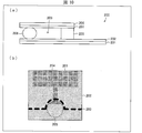
- FIG. 1A is a view of the electrowetting device 1 before being bonded using a sealing material, as viewed from the common electrode substrate 2 side
- FIG. 1B is a view of FIG.
- FIG. 2 is a cross-sectional view taken along the line AB and showing a schematic configuration of the electrowetting device 1.
- the common electrode substrate 2 is provided with a plurality of through holes, and some of the plurality of through holes are injection ports 6 for injecting droplets. The remaining part of the plurality of through holes is a discharge port 13 for discharging gas.
- the common electrode substrate 2 is provided with a total of five through holes, four of which are the inlets 6 for injecting oil as droplets or non-conductive liquid, and the other one is for discharging gas
- the present invention is not limited to this, and it goes without saying that the number of through holes, the number of injection ports 6 and the number of discharge ports 13 can be appropriately changed.
- region illustrated with the pattern of a dotted pattern in (a) of FIG. 1 is a 1st hydrophobic layer 12 and the 2nd hydrophobic layer 5 when the electrowetting apparatus 1 is seen from the common electrode substrate 2 side.
- the region in which at least one of them is formed is shown.
- the shape changes depending on the position and number of the inlets 6 provided in the common electrode substrate 2 and the position and number of the outlets 13.
- the flow path of the droplet is formed by the first hydrophobic layer 12 and the second hydrophobic layer 5 facing each other.
- oil as a non-conductive liquid that is not mixed with the droplet is injected into the flow path.
- a space (one point in the figure) for releasing oil for removing the oil corresponding to the volume of the droplet.
- the active substrate 7 includes a first substrate 8, a thin film transistor (TFT) formation layer 9 formed on the first substrate 8, and a thin film transistor (TFT) formation layer 9. Covering the first electrode layer 10 and the first electrode layer 10 formed on the thin film transistor (TFT) forming layer 9 to form each first electrode electrically connected to the drain electrode of each thin film transistor And a first hydrophobic layer 12 having a surface tension smaller than that of the dielectric layer 11 and formed on the dielectric layer 11.
- the first electrode is an AM (active matrix) electrode, and M ⁇ N (M and N are arbitrary numbers) are formed in an array on the thin film transistor (TFT) formation layer 9.
- AM active matrix
- TFT thin film transistor
- the dielectric layer 11 is formed on the thin film transistor (TFT) formation layer 9 and the first electrode layer 10 so as to cover the plurality of first electrodes, and separates the first electrode layer 10 from the first hydrophobic layer 12. .
- TFT thin film transistor
- the common electrode substrate 2 has a lower surface tension than the second substrate 3, the second electrode layer 4 as a common electrode layer formed on the second substrate 3, and the second electrode layer 4. And a second hydrophobic layer 5 formed on the two-electrode layer 4.
- the second hydrophobic layer 5 in the common electrode substrate 2 is diluted with 1 wt% of “Cytop (registered trademark) -CTL107MK” (trade name) manufactured by AGC Asahi Glass Co., Ltd., which is a perfluoroamorphous resin.
- the opening patterns 5a and 5b are formed by using the patterning method to be described later.
- the present invention is not limited to this.
- the second hydrophobic layer 5 may be formed on the second electrode layer 4 by using a slit coating method or a dip coating method. When the dip coating method is used, the second electrode layer 4 is provided.
- the entire second substrate 3 may be immersed in a 1 wt% dilution of “CYTOP (registered trademark) -CTL107MK” (trade name).
- the first hydrophobic layer 12 in the active substrate 7 is a 1 wt% diluted solution of “Cytop (registered trademark) -CTL107MK” (trade name) manufactured by AGC Asahi Glass Co., Ltd., which is a perfluoro amorphous resin. Is formed on the dielectric layer 11 by a spin coating method, and then a patterning method to be described later is used to form the opening patterns 12a and 12b.
- the first hydrophobic layer 12 may be formed on the dielectric layer 11 by using a slit coating method or a dip coating method. When the dip coating method is used, the first substrate provided with the dielectric layer 11 is used. The whole 8 may be immersed in a 1 wt% dilution of “CYTOP (registered trademark) -CTL107MK” (trade name).
- the first hydrophobic layer 12 and the second hydrophobic layer 5 are formed using a spin coating method, the dilution of “CYTOP (registered trademark) -CTL107MK” (trade name) is performed.
- the film thickness of the first hydrophobic layer 12 and the second hydrophobic layer 5 can be appropriately adjusted by appropriately adjusting the degree and the number of revolutions per minute (rpm) of the spin coater.
- the opening patterns 12a and 12b in the first hydrophobic layer 12 and the opening patterns 5a and 5b in the second hydrophobic layer 5 are both opening patterns for providing a sealing material, and the opening pattern 12a in the first hydrophobic layer 12 is the first pattern. 2
- the opening pattern 5a in the hydrophobic layer 5 is formed so as to overlap in plan view, and the opening pattern 12b in the first hydrophobic layer 12 is formed so as to overlap with opening pattern 5b in the second hydrophobic layer 5 in plan view. Has been.
- the opening pattern 12a in the first hydrophobic layer 12 and the opening pattern 5a in the second hydrophobic layer 5 use oil for removing the oil corresponding to the volume of the droplet when the droplet is injected from the injection port 6.
- the opening pattern 12b in the first hydrophobic layer 12 and the opening pattern 5b in the second hydrophobic layer 5 are for bonding the peripheral portions.
- FIG. 2A is a view of the electrowetting device 1 after being bonded using the sealing material 14 as viewed from the common electrode substrate 2 side
- FIG. 2B is a view of FIG. 2 is a cross-sectional view taken along the line CD of FIG. 2 and shows a schematic configuration of the electrowetting device 1.
- the opening patterns 12 a and 12 b in the first hydrophobic layer 12 and the opening patterns 5 a and 5 b in the second hydrophobic layer 5 are provided with a sealing material 14.
- the common electrode substrate 2 and the active substrate 7 are bonded to each other through the sealing material 14.
- the sealing material 14 is formed so as not to contact both side surfaces of the opening patterns 12a and 12b in the first hydrophobic layer 12 and the opening patterns 5a and 5b in the second hydrophobic layer 5.
- 12b and the opening patterns 5a and 5b are formed to have a lateral width of 3 mm, and the viscosity of the sealing material 14 is adjusted to be relatively high, along the central portions of the opening patterns 12a and 12b and the opening patterns 5a and 5b.
- the sealing material 14 was drawn with a predetermined width, and the width after bonding was 1.5 mm. Accordingly, the distance from the both side surfaces of the opening patterns 12a and 12b and the opening patterns 5a and 5b to the sealing material 14 is 0.75 mm.
- the width of the opening patterns 12a and 12b and the opening patterns 5a and 5b and the width of the sealing material 14 can of course be changed as needed.
- the width of each of the opening patterns 12a, 12b, 5a, and 5b May be different.
- the sealing material 14 is provided not only on the opening patterns 12 a and 12 b in the first hydrophobic layer 12 of the active substrate 7 but also on the opening patterns 5 a and 5 b in the second hydrophobic layer 5 of the common electrode substrate 2.
- the present invention is not limited to this, and the common electrode substrate 2 and the active substrate 7 may be bonded together via the sealing material 14 provided in the opening patterns 12a and 12b in the first hydrophobic layer 12 of the active substrate 7.
- the common electrode substrate 2 and the active substrate 7 may be bonded to each other through the sealing material 14 provided in the opening patterns 5a and 5b in the second hydrophobic layer 5 of the common electrode substrate 2.
- a sealing material 14 may be provided on at least one of the common electrode substrate 2 and the active substrate 7, and the common electrode substrate 2 and the active substrate 7 may be bonded together via the sealing material 14. .
- an epoxy-based sealing material that is an epoxy group-containing sealing material is used as the sealing material 14, and the dielectric layer 11 has a surface tension greater than that of the first hydrophobic layer 12, and the second electrode Since the surface tension of the layer 4 is larger than that of the second hydrophobic layer 5, the sealing material 14 is repelled on the first hydrophobic layer 12 and the second hydrophobic layer 5, but the opening patterns 12 a and 12 b in the first hydrophobic layer 12. It is not repelled on the dielectric layer 11 exposed from and the second electrode layer 4 exposed from the opening patterns 5a and 5b in the second hydrophobic layer 5.
- the contact angle between the sealing material 14 and the dielectric layer 11 made of SiN (silicon nitride) or the second electrode layer 4 made of ITO (indium tin oxide) is such that the sealing material 14 and the first hydrophobic layer 12 Or smaller than the contact angle with the second hydrophobic layer 5.
- a spacer or the like may be used as necessary to secure a gap between the common electrode substrate 2 and the active substrate 7, and this spacer may be included in the sealing material 14.
- an opening pattern is formed in the second electrode layer 4 overlapping the inlet 6 in plan view, and the second hydrophobic layer is formed.
- An opening pattern 5 c is also formed on the layer 5.
- the droplet injected from the injection port 6 is a gap between the common electrode substrate 2 and the active substrate 7, that is, the second hydrophobic layer 5 of the common electrode substrate 2 and the active substrate 7. It is injected into a minute channel (micro channel) formed by a gap between the first hydrophobic layer 12.
- a conductive liquid such as an ionic liquid or a polar liquid
- liquids such as water, an electrolytic solution (electrolyte aqueous solution), alcohols, and various ionic liquids can be used.
- droplets include, for example, whole blood specimens, bacterial cell suspensions, protein or antibody solutions, and various buffer solutions.
- oil as a non-conductive liquid that is not mixed with the liquid droplets may be injected into the minute channel.
- the volume not occupied by the droplets in the minute flow path may be filled with oil.
- non-conductive liquid a non-polar liquid (non-ionic liquid) having a surface tension smaller than that of a droplet can be used.
- non-conductive liquid examples include decane, dodecane, and hexadecane.
- hydrocarbon solvents low molecular hydrocarbon solvents
- undecane oils
- silicone oil examples include dimethylpolysiloxane. Note that only one type of non-conductive liquid may be used, or a plurality of types may be mixed as appropriate.
- the gap between the common electrode substrate 2 and the active substrate 7 that is, the gap between the second hydrophobic layer 5 of the common electrode substrate 2 and the first hydrophobic layer 12 of the active substrate 7.
- the droplets injected into the formed microchannel (microchannel) were formed on the thin film transistor (TFT) forming layer 9 in an array by the first electrode layer 10 in the active substrate 7.
- TFT thin film transistor
- a predetermined voltage is applied to the first electrode (AM (active matrix) electrode) in a predetermined sequence.
- a part (a predetermined amount of finer droplets) is torn off (separated) from the droplets and is carried to a predetermined channel.
- the method of manufacturing the electrowetting device 1 includes a step of forming a thin film transistor (TFT) forming layer 9 on the first substrate 8 and a step of forming the first electrode layer 10 on the thin film transistor (TFT) forming layer 9.
- a step of forming an active substrate 7 including a step of forming a second electrode layer 4 on the second substrate 3, and a second hydrophobic layer 5 having a surface tension smaller than that of the second electrode layer 4 on the second electrode layer 4.
- a step of forming the common electrode substrate 2 including the step of forming the active substrate 7 and the common electrode substrate 2, and the first hydrophobic layer 12 and the second hydrophobic layer 5 are opposed to each other. As shown in FIG. Including a step of, the.
- FIG. 3 is a diagram illustrating an example of a process of forming the first hydrophobic layer 12 having an opening pattern on the dielectric layer 11 in the process of forming the active substrate 7.
- a positive resist film 15 was formed on the dielectric layer 11 by using a spin coat method, a slit coat method, a dip coat method, or the like.
- CYTOP registered trademark
- CTL107MK perfluoroamorphous resin
- the positive resist film 15 and the first hydrophobic layer 12 formed on the positive resist film 15 are stripped using a stripping solution 17. At this time, by applying ultrasonic waves, it is possible to shorten the time required for peeling between the positive resist film 15 and the first hydrophobic layer 12 formed on the positive resist film 15.
- the present invention is not limited to this, and a negative resist film may be used.
- FIG. 4 is a diagram showing another example of the step of forming the first hydrophobic layer 12 having the opening pattern on the dielectric layer 11 in the step of forming the active substrate 7.
- a positive resist film 25 is formed on the first hydrophobic layer 12 by using a spin coat method, a slit coat method, a dip coat method, or the like. .
- the present invention is not limited to this, and a negative resist film may be used.
- the second hydrophobic layer having an opening pattern on the second electrode layer 4 is also used in the process of forming the common electrode substrate 2 by using a process similar to the process illustrated in FIG. 3 or FIG. Layer 5 can be formed.
- the first hydrophobic layer 12 is formed in the step of forming the first hydrophobic layer 12 on the dielectric layer 11 and the step of forming the second hydrophobic layer 5 on the second electrode layer 4.
- the sealing material 14 is formed on the opening patterns 12a and 12b and the opening patterns 5a and 5b formed in the second hydrophobic layer 5, the active substrate 7 and the common electrode substrate 2 have a gap, and the first It bonded together through the sealing material 14 so that the hydrophobic layer 12 and the said 2nd hydrophobic layer 5 might mutually oppose.
- the opening pattern is formed in both the first hydrophobic layer 12 and the second hydrophobic layer 5 has been described as an example.
- the present invention is not limited to this, and the first hydrophobic layer 12 and An opening pattern may be formed only in one of the second hydrophobic layers 5.
- the opening pattern 12a in the first hydrophobic layer 12 is formed so as to overlap the opening pattern 5a in the second hydrophobic layer 5 in plan view
- the opening pattern 12b in the first hydrophobic layer 12 is
- the opening pattern 5b in the second hydrophobic layer 5 is formed so as to overlap with the planar view. However, these may be partially overlapped. It does not have to be.
- the sealing material 14 can be formed with high accuracy to a satisfactory level, and the layer in contact with the sealing material 14 has a higher surface tension than the first hydrophobic layer 12 or the surface of the dielectric layer 11 or the second hydrophobic layer 5. This is because the second electrode layer 4 having a high tension is used, so that the adhesion characteristics between the bonded active substrate 7 and the common electrode substrate 2 can be favorably maintained.
- the sealing material 14 since the sealing material 14 is drawn with high accuracy following the opening patterns 12a, 12b, 5a, and 5b, the sealing material 14 overlaps the inlet 6 and the outlet 13. In order to prevent this, since it is not necessary to widen the interval, the electrowetting device 1 can be downsized.
- the seal material 14 is drawn with high accuracy by the opening patterns 12a, 12b, 5a, and 5b, so that a high-precision dispenser device of the mark recognition alignment method is not required, and the manufacturing cost is increased. Can be suppressed.
- Embodiment 2 of the present invention will be described with reference to FIG.
- This embodiment is different from the first embodiment in that the lateral width of the opening patterns 12c, 12d, 5d, and 5e is further narrowed, and the others are as described in the first embodiment.
- members having the same functions as those shown in the drawings of Embodiment 1 are given the same reference numerals, and descriptions thereof are omitted.
- FIG. 5A is a view of the electrowetting device 21 after being bonded using the sealing material 24 as viewed from the common electrode substrate 22 side
- FIG. 5B is a view of FIG. 2 is a cross-sectional view taken along the line EF of FIG. 2 and shows a schematic configuration of the electrowetting device 21.
- the second hydrophobic layer 5 of the common electrode substrate 22 of the electrowetting device 21 has an opening pattern 5c. 5d is formed, and the opening patterns 12c and 12d having a lateral width of 1 mm are also formed in the first hydrophobic layer 12 of the active substrate 27 of the electrowetting device 21.
- the sealing material 24 is drawn along the opening patterns 12c, 12d, 5d, and 5e so as to cover both side surfaces of the opening patterns 12c, 12d, 5d, and 5e.
- the sealing material 24 can be drawn with higher definition, the electrowetting device 21 can be further reduced in size.
- the sealing material 24 completely fills the opening patterns 12c, 12d, 5d, and 5e, it is possible to suppress a drop in the moving speed of the droplets that may be generated by the opening patterns 12c, 12d, 5d, and 5e.
- Embodiment 3 of the present invention will be described based on FIGS.
- the present embodiment is different from the first and second embodiments in that the electrowetting device 31 is a method of injecting droplets from the side, and the other is as described in the first and second embodiments.
- the electrowetting device 31 is a method of injecting droplets from the side, and the other is as described in the first and second embodiments.
- members having the same functions as those shown in the drawings of Embodiments 1 and 2 are given the same reference numerals, and descriptions thereof are omitted.
- FIG. 6 is a diagram showing a schematic configuration of an electrowetting device 31 of a system for injecting droplets from the side.
- the active substrate 35 includes a first substrate 44, a thin film transistor (TFT) formation layer 48 formed on the first substrate 44, and a thin film transistor (TFT) formation layer 42 formed on the thin film transistor (TFT) formation layer 42.
- the layer 46 includes a first hydrophobic layer 37 having a surface tension smaller than that of the dielectric layer 46 and formed on the dielectric layer 46.
- the first substrate 44, the thin film transistor (TFT) formation layer 42, the first electrode layer 45, and the dielectric layer 46 are collectively referred to as a TFT substrate 36.
- the common electrode substrate 32 has a surface tension smaller than that of the second substrate 42, the second electrode layer 43 as a common electrode layer formed on the second substrate 42, and the second electrode layer 43. And a second hydrophobic layer 34 formed on the two-electrode layer 43.
- the second substrate 42 and the second electrode layer 43 are collectively referred to as a second electrode substrate 33.
- the opening pattern 37a is formed in the first hydrophobic layer 37, and the opening pattern 34a is formed in the second hydrophobic layer 34, and the sealing material 38 is drawn along the opening pattern 37a and the opening pattern 34a.
- the opening pattern 37a and the opening pattern 34a are not formed, but the opening 39 of the sealing material 38 in which the sealing material 38 is interrupted is formed. Has been.
- FIG. 7A is a diagram showing the active substrate 35 before forming the sealing material 38
- FIG. 7B is a diagram showing the active substrate 35 after forming the sealing material 38
- FIG. 6C is a diagram showing a schematic configuration of the electrowetting device 31 in which the active substrate 35 and the common electrode substrate 32 are bonded together.
- a droplet injection region 40 is formed in order to inject a droplet from the outside, and is formed from the droplet injection region 40.
- the opening 39 of the sealing material 38 serving as a droplet injection path with high accuracy so that the opening pattern 37a is formed in the first hydrophobic layer 37. Is formed.
- an opening pattern is formed in both the first hydrophobic layer 37 and the second hydrophobic layer 34, and the opening pattern 37a and the opening pattern 34a are planar.
- the present invention is not limited to this, and any one of the first hydrophobic layer 37 and the second hydrophobic layer 34 may be used as long as the opening 39 of the sealing material 38 can be formed.
- An opening pattern may be formed, and the opening pattern 37a and the opening pattern 34a may partially overlap or may not overlap in plan view.
- the sealing material 38 is drawn along the opening pattern 37a, so that the opening 39 of the sealing material 38 in which the sealing material 38 is interrupted is formed. .
- the active substrate 35 is larger than the common electrode substrate 32, and a part of the first hydrophobic layer 37 formed on the active substrate 35;
- the common electrode substrate 32 and the active substrate 35 are bonded to each other through a sealing material 38 so that the second hydrophobic layer 34 formed on the common electrode substrate 32 faces each other.
- the flow path of the droplet 41 is formed by the first hydrophobic layer 37 and the second hydrophobic layer 34 facing each other. Oil 47 as a non-conductive liquid that is not mixed with the droplets 41 is injected into the flow path.
- the inlet for injecting the droplets and the outlet for discharging the gas in the flow path of the droplets 41 are provided in the seal member 38. 39 can be formed.
- FIG. 8 is a diagram showing a schematic configuration of an electrowetting device 51 including a droplet injection mechanism 50 that guides the droplet 41 to the droplet injection region.
- the electrowetting device 51 including the droplet injection mechanism 50 that guides the droplet 41 injected from above to the droplet injection region 40 (see FIG. 7) is described above.
- the droplet 41 can be injected from above.
- the opening pattern becomes a structural mechanism for controlling the spread of the sealing material 38, and the sealing material 38 can be formed with high accuracy to the extent that the sealing material 38 can be satisfied.
- the layer in contact with the material 38 becomes the dielectric layer 46 having a surface tension larger than that of the first hydrophobic layer 37 or the second electrode layer 43 having a surface tension larger than that of the second hydrophobic layer 34.
- the adhesion property between the substrate 35 and the common electrode substrate 32 can be maintained satisfactorily.
- the opening 39 of the sealing material 38 can be formed with high accuracy.
- the sealing material 38 is drawn with high accuracy by the opening pattern, a high-accuracy dispenser device of a mark recognition alignment method becomes unnecessary, and an increase in manufacturing cost can be suppressed.
- An electrowetting device includes a first substrate, a first electrode layer formed on the first substrate, a dielectric layer formed so as to cover the first electrode layer, An active substrate having a surface tension smaller than that of the dielectric layer and having a first hydrophobic layer formed on the dielectric layer, a second substrate, and a first substrate formed on the second substrate
- An electrowetting device comprising: a two-electrode layer; and a common electrode substrate having a surface tension smaller than that of the second electrode layer and a second hydrophobic layer formed on the second electrode layer.
- An opening pattern is formed in at least one of the first hydrophobic layer and the second hydrophobic layer, and the active substrate and the common electrode substrate include the first hydrophobic layer and the second hydrophobic layer. And the opening pattern so that Through made seal member is characterized by being bonded with a gap.
- an opening pattern is formed in at least one of the first hydrophobic layer and the second hydrophobic layer, and the sealing material is formed in the opening pattern. It becomes a structural mechanism for controlling the spread of the sealing material, and the sealing material can be formed with high accuracy to the satisfaction.
- At least one of the layers in contact with the sealing material is a dielectric layer having a surface tension larger than that of the first hydrophobic layer, or the second electrode having a surface tension larger than that of the second hydrophobic layer. Since it becomes a layer, the adhesion characteristics between the bonded active substrate and the common electrode substrate can be favorably maintained. That is, the peel strength between the bonded active substrate and the common electrode substrate can be favorably maintained.
- the electrowetting device according to aspect 2 of the present invention is the electrowetting device according to aspect 1, in which the opening pattern is formed in each of the first hydrophobic layer and the second hydrophobic layer, and is formed in the first hydrophobic layer.
- the first opening pattern which is the opened pattern and the second opening pattern which is the opening pattern formed in the second hydrophobic layer may partially overlap in plan view.
- the adhesion characteristics between the bonded active substrate and the common electrode substrate can be maintained better.
- the electrowetting device according to aspect 3 of the present invention is the electrowetting device according to aspect 1, in which the opening pattern is formed in each of the first hydrophobic layer and the second hydrophobic layer, and is formed in the first hydrophobic layer.
- the first opening pattern that is the opening pattern and the second opening pattern that is the opening pattern formed in the second hydrophobic layer may overlap in plan view.
- the adhesion characteristics between the bonded active substrate and the common electrode substrate can be maintained better.
- the electrowetting device according to aspect 4 of the present invention is the electrowetting device according to aspect 2, in which the common electrode substrate is provided with a plurality of through holes, and the through holes have the first hydrophobic layer and the through hole in a plan view. It may overlap with the second opening pattern.
- an electrowetting device in which a plurality of through holes are provided in the common electrode substrate can be realized.
- a part of the plurality of through holes may be an injection port for injecting a droplet into the gap.
- the remaining part of the plurality of through holes may be a discharge port for discharging the gas in the gap.
- the electrowetting device according to aspect 7 of the present invention is the electrowetting device according to any one of aspects 1 to 3, wherein the active substrate is larger than the common electrode substrate, and the active substrate and the common electrode substrate overlap in plan view.
- a liquid droplet injection region for injecting liquid droplets into the gap is provided on the first hydrophobic layer of the active substrate, and the first electrode layer is formed in the plan view in the plan view.
- the opening pattern may be formed so as to overlap the droplet injection region and not formed on the first electrode layer overlapping the droplet injection region in plan view.
- an electrowetting device that injects droplets from the side can be realized.
- the sealing material in any of Aspects 1 to 7, may be formed so as not to contact both side surfaces of the opening pattern.
- an electrowetting device in which the sealing material is drawn with high accuracy can be realized.
- the sealing material in any one of Aspects 1 to 7, may be formed so as to cover both side surfaces of the opening pattern.
- the sealing material may be a sealing material containing an epoxy group.
- an electrowetting apparatus that can be bonded to the active substrate and the common electrode substrate by heat treatment can be realized.
- the electrowetting device is the liquid droplet injection mechanism according to aspect 7, in which the liquid droplets injected from above onto the liquid droplet injection region are guided to the liquid droplet injection region. May be provided.
- an electrowetting device that can inject droplets from above can be realized.
- a method for manufacturing an electrowetting device includes a step of forming a first electrode layer on a first substrate, a step of forming a dielectric layer covering the first electrode layer, and the dielectric Forming a first hydrophobic layer having a surface tension lower than that of the dielectric layer on the layer, forming an active substrate, forming a second electrode layer on the second substrate, and the second Forming a second hydrophobic layer having a surface tension smaller than that of the second electrode layer on the electrode layer, and forming a common electrode substrate, the active substrate and the common electrode substrate having a gap
- a method of manufacturing an electrowetting device including a step of bonding through a sealing material so that the first hydrophobic layer and the second hydrophobic layer face each other, wherein the dielectric layer Forming a first hydrophobic layer thereon; And at least one of the steps of forming the second hydrophobic layer on the second electrode layer includes a step of forming an opening pattern in the hydrophobic layer, and in the bonding step
- an opening pattern is formed in the hydrophobic layer in at least one of the step of forming the first hydrophobic layer on the dielectric layer and the step of forming the second hydrophobic layer on the second electrode layer.
- the sealing material is formed on the opening pattern. Therefore, the opening pattern serves as a structural mechanism for controlling the expansion of the sealing material, so that the sealing material can be satisfied. It can be formed with high accuracy.
- At least one of the layers in contact with the sealing material is a dielectric layer having a surface tension larger than that of the first hydrophobic layer, or the second electrode having a surface tension larger than that of the second hydrophobic layer. Since it becomes a layer, the adhesion characteristics between the bonded active substrate and the common electrode substrate can be favorably maintained. That is, the peel strength between the bonded active substrate and the common electrode substrate can be favorably maintained.
- the step of forming an opening pattern in the hydrophobic layer includes a first step of forming a resist film in a predetermined pattern, and the resist film
- the method may include a second step of forming the hydrophobic layer so as to cover and a third step of peeling off the resist film and the hydrophobic layer formed on the resist film together.
- the step of forming an opening pattern in the hydrophobic layer includes a first step of forming the hydrophobic layer, and a resist on the hydrophobic layer.
- a second step of forming a film in a predetermined pattern; a third step of forming an opening pattern in the hydrophobic layer by dry etching using the resist film as a mask; and a fourth step of peeling the resist film on the hydrophobic layer And a method including a process.
- the present invention can be used for an electrowetting device and a method for manufacturing an electrowetting device.
- Electrowetting apparatus Common electrode board
- first substrate 10 first electrode layer 11 dielectric layer 12 first hydrophobic layer 12a opening pattern (first opening pattern) 12b Opening pattern (first opening pattern) 12c Opening pattern (first opening pattern) 12d opening pattern (first opening pattern) 13 Discharge port (through hole)
Landscapes
- Chemical & Material Sciences (AREA)
- Health & Medical Sciences (AREA)
- Dispersion Chemistry (AREA)
- Physics & Mathematics (AREA)
- Analytical Chemistry (AREA)
- General Health & Medical Sciences (AREA)
- Hematology (AREA)
- Clinical Laboratory Science (AREA)
- Chemical Kinetics & Catalysis (AREA)
- General Physics & Mathematics (AREA)
- Optics & Photonics (AREA)
- Electrochromic Elements, Electrophoresis, Or Variable Reflection Or Absorption Elements (AREA)
Abstract
La présente invention concerne un dispositif d'électromouillage qui présente un matériau d'étanchéité formé avec une précision élevée satisfaisante tout en maintenant des propriétés adhésives favorables entre deux substrats. Une première couche hydrophobe (12) et une seconde couche hydrophobe (5) ont des motifs d'ouverture (12a, 12b, 5a, 5b) formés dans celles-ci, et un substrat actif (7) et un substrat d'électrode commun (2) sont liés ensemble avec un espace entre eux par l'intermédiaire d'un matériau d'étanchéité (14) formé dans les motifs d'ouverture (12a, 12b, 5a, 5b).
Priority Applications (3)
| Application Number | Priority Date | Filing Date | Title |
|---|---|---|---|
| US16/087,037 US10866404B2 (en) | 2016-03-24 | 2017-03-22 | Electrowetting device and method of manufacturing electrowetting device |
| CN201780019541.0A CN108885379B (zh) | 2016-03-24 | 2017-03-22 | 电润湿装置以及电润湿装置的制造方法 |
| EP17770293.3A EP3435150A4 (fr) | 2016-03-24 | 2017-03-22 | Dispositif d'électromouillage et procédé de fabrication d'un dispositif d'électromouillage |
Applications Claiming Priority (2)
| Application Number | Priority Date | Filing Date | Title |
|---|---|---|---|
| JP2016-060856 | 2016-03-24 | ||
| JP2016060856 | 2016-03-24 |
Publications (1)
| Publication Number | Publication Date |
|---|---|
| WO2017164253A1 true WO2017164253A1 (fr) | 2017-09-28 |
Family
ID=59900288
Family Applications (1)
| Application Number | Title | Priority Date | Filing Date |
|---|---|---|---|
| PCT/JP2017/011522 WO2017164253A1 (fr) | 2016-03-24 | 2017-03-22 | Dispositif d'électromouillage et procédé de fabrication d'un dispositif d'électromouillage |
Country Status (4)
| Country | Link |
|---|---|
| US (1) | US10866404B2 (fr) |
| EP (1) | EP3435150A4 (fr) |
| CN (1) | CN108885379B (fr) |
| WO (1) | WO2017164253A1 (fr) |
Families Citing this family (6)
| Publication number | Priority date | Publication date | Assignee | Title |
|---|---|---|---|---|
| CN108778484B (zh) * | 2016-03-30 | 2023-09-22 | 夏普生命科学(欧洲)有限公司 | 微流体装置 |
| JP2020042261A (ja) * | 2018-09-06 | 2020-03-19 | シャープ株式会社 | エレクトロウェッティング装置 |
| CN111545259B (zh) * | 2020-04-28 | 2021-11-23 | 上海天马微电子有限公司 | 电润湿面板以及反应装置 |
| US20220126287A1 (en) * | 2020-05-13 | 2022-04-28 | Boe Technology Group Co., Ltd. | Micro-fluidic chip, liquid loading method thereof and micro-fluidic system |
| WO2023027779A1 (fr) * | 2021-08-26 | 2023-03-02 | Flexterra, Inc. | Système d'électromouillage sur demande avec transistors organiques |
| TWI814434B (zh) * | 2022-04-01 | 2023-09-01 | 友達光電股份有限公司 | 發光二極體陣列基板 |
Citations (5)
| Publication number | Priority date | Publication date | Assignee | Title |
|---|---|---|---|---|
| JP2009031795A (ja) * | 2007-07-25 | 2009-02-12 | Innolux Display Corp | エレクトロウエッティングディスプレイ |
| WO2012039471A1 (fr) * | 2010-09-22 | 2012-03-29 | 積水化学工業株式会社 | Écran à électromouillage |
| US20120154886A1 (en) * | 2009-08-14 | 2012-06-21 | University Of Cincinnati | Display pixels, displays, and methods of operating display pixels |
| JP2013542465A (ja) * | 2010-10-29 | 2013-11-21 | ミオールテック ホールディング ビー.ブイ. | エレクトロウェッティング光学素子 |
| JP2015022104A (ja) * | 2013-07-18 | 2015-02-02 | ソニー株式会社 | 表示装置および電子機器 |
Family Cites Families (23)
| Publication number | Priority date | Publication date | Assignee | Title |
|---|---|---|---|---|
| FR2887030B1 (fr) * | 2005-06-09 | 2008-06-13 | Commissariat Energie Atomique | Dispositif planaire avec adressage de puits automatise par electromouillage dynamique |
| JP2008052048A (ja) | 2006-08-24 | 2008-03-06 | Toshiba Matsushita Display Technology Co Ltd | 液晶表示装置 |
| WO2008063135A1 (fr) * | 2006-11-24 | 2008-05-29 | Agency For Science, Technology And Research | Appareil pour traiter un échantillon dans une gouttelette de liquide et procédé d'utilisation |
| CN101663089A (zh) | 2007-04-04 | 2010-03-03 | 微点生物技术有限公司 | 微机械加工的电润湿微流体阀 |
| WO2009076414A2 (fr) * | 2007-12-10 | 2009-06-18 | Advanced Liquid Logic, Inc. | Configurations d'actionneur de gouttelette et procédés |
| GB0724736D0 (en) * | 2007-12-19 | 2008-01-30 | Oxford Nanolabs Ltd | Formation of layers of amphiphilic molecules |
| CN101493576B (zh) * | 2008-01-23 | 2010-12-15 | 财团法人工业技术研究院 | 电润湿法显示器装置及其制造方法 |
| US20110140996A1 (en) * | 2009-12-15 | 2011-06-16 | Lesley Anne Parry-Jones | Switchable transmissive/reflective electrowetting display |
| JP2012181513A (ja) * | 2011-02-10 | 2012-09-20 | Daikin Ind Ltd | エレクトロウエッティング用疎水性誘電体フィルム |
| KR101962963B1 (ko) * | 2012-03-20 | 2019-08-01 | 리쿠아비스타 비.브이. | 전기습윤 표시 장치 |
| KR102027586B1 (ko) * | 2012-08-06 | 2019-10-02 | 리쿠아비스타 비.브이. | 전기습윤 표시장치 및 이의 제조 방법 |
| JP2014052561A (ja) | 2012-09-07 | 2014-03-20 | Fujifilm Corp | 光学素子及び画像表示装置 |
| CN102998791B (zh) * | 2012-12-03 | 2015-04-01 | 京东方科技集团股份有限公司 | 一种电润湿显示装置 |
| EP2869922B1 (fr) | 2013-01-09 | 2019-11-20 | Tecan Trading AG | Cartouches jetables pour un système microfluidique |
| US9207450B1 (en) * | 2014-06-27 | 2015-12-08 | Amazon Technologies, Inc. | Insulated notch design for pixels in an electrowetting device |
| CN104330891A (zh) | 2014-10-22 | 2015-02-04 | 深圳市华星光电技术有限公司 | 电湿润显示面板及电湿润显示装置 |
| US9810899B1 (en) * | 2014-12-23 | 2017-11-07 | Amazon Technologies, Inc. | Illumination of an electrowetting display |
| CN104678547A (zh) * | 2015-02-02 | 2015-06-03 | 华南师范大学 | 电润湿基板及其制造方法、电润湿显示器件 |
| CN105093519A (zh) * | 2015-08-13 | 2015-11-25 | 信利半导体有限公司 | 一种电润湿显示面板、显示装置及显示面板的显示方法 |
| US10061117B1 (en) * | 2016-03-18 | 2018-08-28 | Amazon Technologies, Inc. | Electrowetting display pixel walls and spacers |
| JP6494580B2 (ja) * | 2016-09-28 | 2019-04-03 | シャープ ライフ サイエンス (イーユー) リミテッド | 微小流体装置 |
| US10369570B2 (en) | 2017-07-27 | 2019-08-06 | Sharp Life Science (Eu) Limited | Microfluidic device with droplet pre-charge on input |
| JP2019061037A (ja) * | 2017-09-26 | 2019-04-18 | シャープ株式会社 | エレクトロウェッティング装置及びエレクトロウェッティング装置の製造方法 |
-
2017
- 2017-03-22 WO PCT/JP2017/011522 patent/WO2017164253A1/fr active Application Filing
- 2017-03-22 EP EP17770293.3A patent/EP3435150A4/fr not_active Withdrawn
- 2017-03-22 CN CN201780019541.0A patent/CN108885379B/zh active Active
- 2017-03-22 US US16/087,037 patent/US10866404B2/en active Active
Patent Citations (5)
| Publication number | Priority date | Publication date | Assignee | Title |
|---|---|---|---|---|
| JP2009031795A (ja) * | 2007-07-25 | 2009-02-12 | Innolux Display Corp | エレクトロウエッティングディスプレイ |
| US20120154886A1 (en) * | 2009-08-14 | 2012-06-21 | University Of Cincinnati | Display pixels, displays, and methods of operating display pixels |
| WO2012039471A1 (fr) * | 2010-09-22 | 2012-03-29 | 積水化学工業株式会社 | Écran à électromouillage |
| JP2013542465A (ja) * | 2010-10-29 | 2013-11-21 | ミオールテック ホールディング ビー.ブイ. | エレクトロウェッティング光学素子 |
| JP2015022104A (ja) * | 2013-07-18 | 2015-02-02 | ソニー株式会社 | 表示装置および電子機器 |
Non-Patent Citations (1)
| Title |
|---|
| See also references of EP3435150A4 * |
Also Published As
| Publication number | Publication date |
|---|---|
| CN108885379B (zh) | 2021-10-12 |
| EP3435150A1 (fr) | 2019-01-30 |
| CN108885379A (zh) | 2018-11-23 |
| US10866404B2 (en) | 2020-12-15 |
| US20190107709A1 (en) | 2019-04-11 |
| EP3435150A4 (fr) | 2019-03-13 |
Similar Documents
| Publication | Publication Date | Title |
|---|---|---|
| WO2017164253A1 (fr) | Dispositif d'électromouillage et procédé de fabrication d'un dispositif d'électromouillage | |
| TWI442088B (zh) | 電濕潤顯示元件 | |
| WO2017078059A1 (fr) | Dispositif d'électromouillage, son procédé de fabrication, et procédé d'injection de gouttelettes | |
| CN112136205A (zh) | 使用差分润湿引发液滴的运动 | |
| KR101967472B1 (ko) | 전기습윤 표시 장치 및 이의 제조 방법 | |
| KR101787240B1 (ko) | 표시 장치 | |
| US20120293857A1 (en) | Electrophoretic Display Apparatus and Method for Manufacturing the Same | |
| US20180059056A1 (en) | Electrowetting on dielectric device including surfactant containing siloxane group | |
| JP2018051685A (ja) | 微小流体装置 | |
| CN104603595A (zh) | 用于减少气泡形成的技术和液滴致动器设计 | |
| US20100108232A1 (en) | Method for fabricating electrowetting displays | |
| TWI804778B (zh) | 包括用於數位微流體的空間可變疏水層之數位微流體裝置及其製造方法 | |
| CN109891569B (zh) | 元件拾取装置及其制备方法、使用方法 | |
| KR20130143150A (ko) | 전기 습윤 표시 장치 및 이의 제조 방법 | |
| US11442264B2 (en) | Electrowetting device | |
| CN109557659B (zh) | 电润湿装置及电润湿装置的制造方法 | |
| JP2016109499A (ja) | 液滴駆動装置およびその製造方法 | |
| EP3160656B1 (fr) | Procédé de fabrication d'un élément d'électromouillage | |
| CN108472620B (zh) | 电极基板以及其制造方法、电子设备 | |
| US20220193677A1 (en) | Foldable digital microfluidic (dmf) device using flexible electronic platform and methods of making same | |
| US20140192465A1 (en) | Through connection of a display device | |
| CN108778484B (zh) | 微流体装置 | |
| US10557567B2 (en) | Fluidic micro electromechanical system | |
| US9841594B2 (en) | Apparatus of coupling substrates for electrowetting display panel and method of coupling substrates for electrowetting display using the same | |
| Walton et al. | Building EWOD microfluidic array technology on top of foundry CMOS |
Legal Events
| Date | Code | Title | Description |
|---|---|---|---|
| NENP | Non-entry into the national phase |
Ref country code: DE |
|
| WWE | Wipo information: entry into national phase |
Ref document number: 2017770293 Country of ref document: EP |
|
| ENP | Entry into the national phase |
Ref document number: 2017770293 Country of ref document: EP Effective date: 20181024 |
|
| 121 | Ep: the epo has been informed by wipo that ep was designated in this application |
Ref document number: 17770293 Country of ref document: EP Kind code of ref document: A1 |
|
| NENP | Non-entry into the national phase |
Ref country code: JP |