WO2017158977A1 - 処理装置及びコリメータ - Google Patents
処理装置及びコリメータ Download PDFInfo
- Publication number
- WO2017158977A1 WO2017158977A1 PCT/JP2016/087818 JP2016087818W WO2017158977A1 WO 2017158977 A1 WO2017158977 A1 WO 2017158977A1 JP 2016087818 W JP2016087818 W JP 2016087818W WO 2017158977 A1 WO2017158977 A1 WO 2017158977A1
- Authority
- WO
- WIPO (PCT)
- Prior art keywords
- frame
- collimator
- axis
- unit
- direction along
- Prior art date
- Legal status (The legal status is an assumption and is not a legal conclusion. Google has not performed a legal analysis and makes no representation as to the accuracy of the status listed.)
- Ceased
Links
Images







Classifications
-
- C—CHEMISTRY; METALLURGY
- C23—COATING METALLIC MATERIAL; COATING MATERIAL WITH METALLIC MATERIAL; CHEMICAL SURFACE TREATMENT; DIFFUSION TREATMENT OF METALLIC MATERIAL; COATING BY VACUUM EVAPORATION, BY SPUTTERING, BY ION IMPLANTATION OR BY CHEMICAL VAPOUR DEPOSITION, IN GENERAL; INHIBITING CORROSION OF METALLIC MATERIAL OR INCRUSTATION IN GENERAL
- C23C—COATING METALLIC MATERIAL; COATING MATERIAL WITH METALLIC MATERIAL; SURFACE TREATMENT OF METALLIC MATERIAL BY DIFFUSION INTO THE SURFACE, BY CHEMICAL CONVERSION OR SUBSTITUTION; COATING BY VACUUM EVAPORATION, BY SPUTTERING, BY ION IMPLANTATION OR BY CHEMICAL VAPOUR DEPOSITION, IN GENERAL
- C23C14/00—Coating by vacuum evaporation, by sputtering or by ion implantation of the coating forming material
- C23C14/22—Coating by vacuum evaporation, by sputtering or by ion implantation of the coating forming material characterised by the process of coating
- C23C14/34—Sputtering
-
- G—PHYSICS
- G02—OPTICS
- G02B—OPTICAL ELEMENTS, SYSTEMS OR APPARATUS
- G02B27/00—Optical systems or apparatus not provided for by any of the groups G02B1/00 - G02B26/00, G02B30/00
- G02B27/30—Collimators
-
- H—ELECTRICITY
- H01—ELECTRIC ELEMENTS
- H01J—ELECTRIC DISCHARGE TUBES OR DISCHARGE LAMPS
- H01J37/00—Discharge tubes with provision for introducing objects or material to be exposed to the discharge, e.g. for the purpose of examination or processing thereof
- H01J37/32—Gas-filled discharge tubes
- H01J37/32009—Arrangements for generation of plasma specially adapted for examination or treatment of objects, e.g. plasma sources
- H01J37/32422—Arrangement for selecting ions or species in the plasma
-
- H—ELECTRICITY
- H01—ELECTRIC ELEMENTS
- H01J—ELECTRIC DISCHARGE TUBES OR DISCHARGE LAMPS
- H01J37/00—Discharge tubes with provision for introducing objects or material to be exposed to the discharge, e.g. for the purpose of examination or processing thereof
- H01J37/32—Gas-filled discharge tubes
- H01J37/34—Gas-filled discharge tubes operating with cathodic sputtering
- H01J37/3402—Gas-filled discharge tubes operating with cathodic sputtering using supplementary magnetic fields
- H01J37/3405—Magnetron sputtering
- H01J37/3408—Planar magnetron sputtering
-
- H—ELECTRICITY
- H01—ELECTRIC ELEMENTS
- H01J—ELECTRIC DISCHARGE TUBES OR DISCHARGE LAMPS
- H01J37/00—Discharge tubes with provision for introducing objects or material to be exposed to the discharge, e.g. for the purpose of examination or processing thereof
- H01J37/32—Gas-filled discharge tubes
- H01J37/34—Gas-filled discharge tubes operating with cathodic sputtering
- H01J37/3411—Constructional aspects of the reactor
- H01J37/3447—Collimators, shutters, apertures
-
- H—ELECTRICITY
- H10—SEMICONDUCTOR DEVICES; ELECTRIC SOLID-STATE DEVICES NOT OTHERWISE PROVIDED FOR
- H10P—GENERIC PROCESSES OR APPARATUS FOR THE MANUFACTURE OR TREATMENT OF DEVICES COVERED BY CLASS H10
- H10P14/00—Formation of materials, e.g. in the shape of layers or pillars
- H10P14/40—Formation of materials, e.g. in the shape of layers or pillars of conductive or resistive materials
- H10P14/42—Formation of materials, e.g. in the shape of layers or pillars of conductive or resistive materials using a gas or vapour
-
- H—ELECTRICITY
- H10—SEMICONDUCTOR DEVICES; ELECTRIC SOLID-STATE DEVICES NOT OTHERWISE PROVIDED FOR
- H10P—GENERIC PROCESSES OR APPARATUS FOR THE MANUFACTURE OR TREATMENT OF DEVICES COVERED BY CLASS H10
- H10P72/00—Handling or holding of wafers, substrates or devices during manufacture or treatment thereof
- H10P72/70—Handling or holding of wafers, substrates or devices during manufacture or treatment thereof for supporting or gripping
Definitions
- Embodiments described herein relate generally to a processing apparatus and a collimator.
- a sputtering apparatus for depositing metal on a semiconductor wafer has a collimator for aligning the direction of metal particles to be deposited.
- the collimator has walls that form a large number of through holes, and allows particles flying in a substantially vertical direction to an object to be processed, such as a semiconductor wafer, to pass therethrough and blocks particles flying obliquely.
- the range of the direction of particles to be deposited is determined by the shape of the collimator. For this reason, when the range of the direction of the particles to be formed changes, the collimator is also replaced.
- a processing apparatus includes an object placement unit, a generation source placement unit, and a collimator.
- the object placement unit is configured to place an object.
- the generation source arrangement unit is arranged at a position separated from the object arrangement unit, and is configured such that a particle generation source capable of emitting particles toward the object is arranged.
- the collimator is configured to be disposed between the object placement unit and the generation source placement unit, and includes a frame and a plurality of first walls, and is formed by the plurality of first walls. A plurality of first through holes extending in a first direction from the source arrangement unit toward the object arrangement unit, and a first rectification unit configured to be detachably attached to the frame.
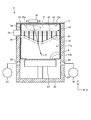
- FIG. 1 is a cross-sectional view schematically showing a sputtering apparatus according to the first embodiment.
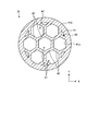
- FIG. 2 is a plan view schematically showing the collimator of the first embodiment.
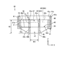
- FIG. 3 is a cross-sectional view schematically showing the collimator of the first embodiment.
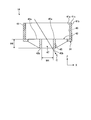
- 4 is a cross-sectional view schematically showing the base component of the first embodiment along the line F4-F4 in FIG.
- FIG. 5 is a cross-sectional view schematically showing a collimator having two collimating components of the first embodiment.
- FIG. 6 is a cross-sectional view schematically showing a collimator having another collimating component of the first embodiment.
- FIG. 1 is a cross-sectional view schematically showing a sputtering apparatus according to the first embodiment.
- FIG. 2 is a plan view schematically showing the collimator of the first embodiment.
- FIG. 3 is a cross-sectional view schematically showing the collimator of the first embodiment.
- 4 is a
- FIG. 7 is a cross-sectional view schematically showing the collimator from which the collimating component of the first embodiment has been removed.
- FIG. 8 is a plan view schematically showing the collimator in which the collimator component of the first embodiment is rotated.
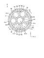
- FIG. 9 is a plan view schematically showing a collimator according to the second embodiment.
- FIG. 10 is a plan view schematically showing the collimator in which the collimator component of the second embodiment is moved.
- FIG. 11 is a cross-sectional view schematically showing a sputtering apparatus according to the third embodiment.
- FIG. 12 is a cross-sectional view schematically showing the collimator of the third embodiment.
- FIG. 13 is a plan view schematically showing a collimator according to a first modification of the third embodiment.
- FIG. 14 is a cross-sectional view schematically showing a collimator according to a second modification of the third embodiment.
- a vertically upward direction is defined as an upward direction and a vertically downward direction is defined as a downward direction.
- a plurality of expressions may be described for the constituent elements according to the embodiment and the description of the elements. Other expressions that are not described may be applied to the components and descriptions in which a plurality of expressions are made. Furthermore, the constituent elements that are not expressed in a plurality of expressions and descriptions may be expressed in other ways that are not described.
- FIG. 1 is a cross-sectional view schematically showing a sputtering apparatus 1 according to the first embodiment.
- the sputtering apparatus 1 is an example of a processing apparatus, and may be referred to as, for example, a semiconductor manufacturing apparatus, a manufacturing apparatus, a processing apparatus, or an apparatus.
- the sputtering apparatus 1 is an apparatus for performing magnetron sputtering, for example.
- the sputtering apparatus 1 forms a film with metal particles on the surface of the semiconductor wafer 2.
- the semiconductor wafer 2 is an example of an object, and may be referred to as a target, for example. Note that the sputtering apparatus 1 may form a film on another target, for example.
- the sputtering apparatus 1 includes a chamber 11, a target 12, a stage 13, a magnet 14, a shielding member 15, a collimator 16, a pump 17, and a tank 18.
- the target 12 is an example of a particle generation source.
- the collimator 16 may also be referred to as a shielding component, a rectifying component, or a direction adjusting component, for example.
- an X axis, a Y axis, and a Z axis are defined.
- the X axis, the Y axis, and the Z axis are orthogonal to each other.
- the X axis is along the width of the chamber 11.
- the Y axis is along the depth (length) of the chamber 11.
- the Z axis is along the height of the chamber 11. In the following description, the Z axis is assumed to be along the vertical direction. Note that the Z axis of the sputtering apparatus 1 may cross obliquely with respect to the vertical direction.
- the chamber 11 is formed in a sealable box shape.
- the chamber 11 includes an upper wall 21, a bottom wall 22, a side wall 23, a discharge port 24, and an introduction port 25.
- the upper wall 21 can also be referred to as a backing plate, a mounting portion, or a holding portion, for example.
- the upper wall 21 and the bottom wall 22 are arranged to face each other in the direction along the Z axis (vertical direction).
- the upper wall 21 is located above the bottom wall 22 with a predetermined interval.
- the side wall 23 is formed in a cylindrical shape extending in the direction along the Z axis, and connects the upper wall 21 and the bottom wall 22.
- a processing chamber 11 a is provided inside the chamber 11.
- the processing chamber 11a can also be referred to as the inside of a container.
- the inner surfaces of the upper wall 21, the bottom wall 22, and the side wall 23 form a processing chamber 11a.
- the processing chamber 11a can be hermetically closed. In other words, the processing chamber 11a can be sealed.
- the airtightly closed state is a state in which no gas moves between the inside and outside of the processing chamber 11a, and the discharge port 24 and the introduction port 25 may be opened in the processing chamber 11a.
- the target 12, the stage 13, the shielding member 15, and the collimator 16 are disposed in the processing chamber 11a.
- the target 12, the stage 13, the shielding member 15, and the collimator 16 are accommodated in the chamber 11.
- the target 12, the stage 13, the shielding member 15, and the collimator 16 may be partially located outside the processing chamber 11a.
- the discharge port 24 opens to the processing chamber 11 a and is connected to the pump 17.
- the pump 17 is, for example, a dry pump, a cryopump, or a turbo molecular pump. When the pump 17 sucks the gas in the processing chamber 11a from the discharge port 24, the atmospheric pressure in the processing chamber 11a can be lowered. The pump 17 can evacuate the processing chamber 11a.
- the inlet 25 opens into the processing chamber 11a and is connected to the tank 18.
- the tank 18 contains an inert gas such as argon gas. Argon gas can be introduced from the tank 18 through the inlet 25 into the processing chamber 11a.
- the tank 18 has a valve capable of stopping the introduction of argon gas.
- the target 12 is, for example, a disk-shaped metal plate used as a particle generation source.
- the target 12 may be formed in other shapes.
- the target 12 is made of, for example, copper.
- the target 12 may be made of other materials.
- the target 12 is attached to the attachment surface 21 a of the upper wall 21 of the chamber 11.
- the upper wall 21 that is a backing plate is used as a coolant and an electrode for the target 12.
- the chamber 11 may have a backing plate as a separate part from the upper wall 21.
- the mounting surface 21a of the upper wall 21 is an inner surface of the upper wall 21 that is formed in a substantially flat direction in the negative direction (downward direction) along the Z axis.
- the target 12 is disposed on the mounting surface 21a.
- the upper wall 21 is an example of a generation source arrangement unit.
- the source arrangement unit is not limited to an independent member or part, and may be a specific position on a certain member or part.
- the negative direction along the Z axis is the opposite direction to the direction in which the arrow on the Z axis faces.
- the negative direction along the Z-axis is a direction from the mounting surface 21a of the upper wall 21 toward the placement surface 13a of the stage 13, and is an example of a first direction.
- the direction along the Z axis and the vertical direction include a negative direction along the Z axis and a positive direction along the Z axis (a direction in which the arrow on the Z axis faces).
- the target 12 has a lower surface 12a.
- the lower surface 12a is a substantially flat surface facing downward.
- FIG. 1 shows the plasma P by a two-dot chain line.
- the magnet 14 is located outside the processing chamber 11a.
- the magnet 14 is, for example, an electromagnet or a permanent magnet.
- the magnet 14 is movable along the upper wall 21 and the target 12.
- the upper wall 21 is located between the target 12 and the magnet 14.
- the plasma P is generated near the magnet 14. For this reason, the target 12 is located between the magnet 14 and the plasma P.
- the target 12 can emit particles C.
- the particle C includes a copper ion, a copper atom, and a copper molecule.
- the direction in which the particles C fly from the lower surface 12a of the target 12 is distributed according to the cosine law (Lambert's cosine law). That is, the particles C flying from one point on the lower surface 12a fly most in the normal direction (vertical direction) of the lower surface 12a.
- the number of particles C flying in a direction inclined at an angle ⁇ with respect to the normal direction (crossing diagonally) is roughly proportional to the cosine (cos ⁇ ) of the number of particles C flying in the normal direction.
- Particle C is an example of a particle in the present embodiment, and is a fine particle of a film forming material that constitutes the target 12.
- the particles may be various particles constituting a substance or energy rays such as molecules, atoms, ions, nuclei, electrons, elementary particles, vapor (vaporized substance), and electromagnetic waves (photons).
- the stage 13 is disposed on the bottom wall 22 of the chamber 11.
- the stage 13 is disposed away from the upper wall 21 and the target 12 in the direction along the Z axis.
- the stage 13 has a placement surface 13a.
- the mounting surface 13 a of the stage 13 supports the semiconductor wafer 2.
- the semiconductor wafer 2 is formed in a disk shape, for example.
- the semiconductor wafer 2 may be formed in other shapes.
- the mounting surface 13a of the stage 13 is a substantially flat surface facing upward.
- the mounting surface 13a is disposed away from the mounting surface 21a of the upper wall 21 in the direction along the Z axis, and faces the mounting surface 21a.
- the semiconductor wafer 2 is arranged on such a mounting surface 13a.
- the stage 13 is an example of an object placement unit.
- the object placement unit is not limited to an independent member or part, and may be a specific position on a certain member or part.
- the stage 13 is movable in the direction along the Z axis, that is, in the vertical direction.
- the stage 13 has a heater and can heat the semiconductor wafer 2 disposed on the mounting surface 13a. Furthermore, the stage 13 is also used as an electrode.
- the shielding member 15 is formed in a substantially cylindrical shape.
- the shielding member 15 covers a part of the side wall 23 and a gap between the side wall 23 and the semiconductor wafer 2.
- the shielding member 15 may hold the semiconductor wafer 2.
- the shielding member 15 suppresses the particles C emitted from the target 12 from adhering to the bottom wall 22 and the side wall 23.
- the collimator 16 is disposed between the mounting surface 21a of the upper wall 21 and the mounting surface 13a of the stage 13 in the direction along the Z axis. According to another expression, the collimator 16 is disposed between the target 12 and the semiconductor wafer 2 in the direction along the Z axis (vertical direction). The collimator 16 is attached to the side wall 23 of the chamber 11, for example. The collimator 16 may be supported by the shielding member 15.
- the collimator 16 and the chamber 11 are insulated.
- an insulating member is interposed between the collimator 16 and the chamber 11. Further, the collimator 16 and the shielding member 15 are also insulated.
- the distance between the collimator 16 and the mounting surface 21 a of the upper wall 21 is shorter than the distance between the collimator 16 and the mounting surface 13 a of the stage 13.
- the collimator 16 is closer to the mounting surface 21 a of the upper wall 21 than the mounting surface 13 a of the stage 13.
- the arrangement of the collimator 16 is not limited to this.
- FIG. 2 is a plan view schematically showing the collimator 16 of the first embodiment.
- FIG. 3 is a cross-sectional view schematically showing the collimator 16 of the first embodiment.
- the collimator 16 has a base part 31 and a collimating part 32.
- the collimating component 32 is an example of a first rectifying unit.
- the base part 31 is made of, for example, aluminum.
- the base part 31 may be made of other materials.
- the base part 31 includes a frame 41 and a rectifying unit 42.
- the frame 41 may also be referred to as an outer edge portion, a holding portion, a support portion, or a wall, for example.
- the rectifying unit 42 is an example of a second rectifying unit.
- the frame 41 is a wall formed in a substantially cylindrical shape extending in the direction along the Z axis.
- the frame 41 is not limited to this, and may be formed in other shapes such as a rectangle.
- the frame 41 has an inner peripheral surface 41a and an outer peripheral surface 41b.
- the inner peripheral surface 41 a of the frame 41 is a curved surface that faces the radial direction of the cylindrical frame 41 and faces the central axis of the cylindrical frame 41.
- the outer peripheral surface 41b is located on the opposite side of the inner peripheral surface 41a. In the XY plane, the area of the portion surrounded by the outer peripheral surface 41 b of the frame 41 is larger than the cross-sectional area of the semiconductor wafer 2.
- the frame 41 covers a part of the side wall 23. Between the upper wall 21 and the stage 13 in the direction along the Z axis, the side wall 23 is covered with the shielding member 15 and the frame 41 of the collimator 16. The frame 41 prevents the particles C emitted from the target 12 from adhering to the side wall 23.
- FIG. 4 is a cross-sectional view schematically showing the base component 31 of the first embodiment along the line F4-F4 in FIG.
- the rectifying unit 42 is provided inside the cylindrical frame 41 in the XY plane.
- the rectifying unit 42 is connected to the inner peripheral surface 41 a of the frame 41.
- the frame 41 and the rectifying unit 42 are made integrally. In other words, the rectifying unit 42 is fixed inside the frame 41. Note that the rectifying unit 42 may be a component independent of the frame 41.
- the rectifying unit 42 is disposed between the mounting surface 21 a of the upper wall 21 and the mounting surface 13 a of the stage 13.
- the rectifying unit 42 is separated from the upper wall 21 and separated from the stage 13 in the direction along the Z axis.
- the rectifying unit 42 has a plurality of first wall portions 45.
- the plurality of first wall portions 45 are an example of a plurality of second walls, and may be referred to as a plate or a shielding portion, for example.
- the rectifying unit 42 forms a plurality of first openings 47 arranged substantially in parallel by the plurality of first wall portions 45.
- the plurality of first openings 47 are an example of a plurality of second through holes.
- the plurality of first openings 47 are hexagonal holes extending in a direction (vertical direction) along the Z axis.
- the plurality of first wall portions 45 form an aggregate (honeycomb structure) of a plurality of hexagonal cylinders having a first opening 47 formed therein.
- the first opening 47 extending in the direction along the Z axis can pass an object such as the particle C moving in the direction along the Z axis.
- the first opening 47 may be formed in other shapes.
- the rectifying unit 42 has an upper end 42a and a lower end 42b.
- the upper end portion 42 a is one end portion in the direction along the Z axis of the rectifying unit 42 and faces the attachment surface 21 a of the target 12 and the upper wall 21.
- the lower end portion 42 b is the other end portion in the direction along the Z axis of the rectifying unit 42, and faces the semiconductor wafer 2 supported by the stage 13 and the mounting surface 13 a of the stage 13.
- 1st opening 47 is provided ranging from the upper end part 42a of the rectification
- Each of the plurality of first wall portions 45 is a substantially rectangular (quadrangle) plate extending in the direction along the Z axis.
- the first wall 45 may extend in a direction that obliquely intersects the direction along the Z axis.
- the first wall portion 45 has an upper end surface 45a and a lower end surface 45b.
- the upper end surface 45a of the first wall portion 45 is one end portion in the direction along the Z axis of the first wall portion 45 and faces the mounting surface 21a of the target 12 and the upper wall 21.
- the upper end surfaces 45 a of the plurality of first wall portions 45 form the upper end portion 42 a of the rectifying unit 42.
- the upper end part 42a of the rectifying part 42 is formed substantially flat.
- the upper end portion 42a may be recessed in a curved shape with respect to the target 12 and the mounting surface 21a of the upper wall 21, for example.
- the upper end portion 42 a may be curved so as to be separated from the target 12 and the mounting surface 21 a of the upper wall 21.
- the lower end surface 45b of the first wall portion 45 is the other end portion in the direction along the Z axis of the first wall portion 45, and is placed on the semiconductor wafer 2 supported by the stage 13 and the mounting surface 13a of the stage 13. Turn to. Lower end surfaces 45b of the plurality of first wall portions 45 form lower end portions 42b of the rectifying unit 42.
- the lower end portion 42 b of the rectifying unit 42 protrudes toward the semiconductor wafer 2 supported by the stage 13 and the mounting surface 13 a of the stage 13. In other words, the lower end portion 42 b of the rectifying unit 42 approaches the stage 13 as it is separated from the frame 41.
- the lower end portion 42b of the rectifying unit 42 may be formed in other shapes.
- the upper end portion 42a and the lower end portion 42b of the rectifying unit 42 have different shapes. For this reason, the rectification
- a plurality of grooves 49 are provided on the inner peripheral surface 41 a of the frame 41.
- the groove 49 is an example of a first holding unit.
- Each of the plurality of grooves 49 extends in a direction along the Z axis.
- the plurality of grooves 49 extend from the upper end portion 42 a of the rectifying unit 42 to the upper end 41 c of the frame 41.
- the groove 49 opens at the upper end 41 c of the frame 41 in the positive direction along the Z axis.
- the upper end 41 c is one end in the direction along the Z axis of the frame 41 and faces the upper wall 21.
- the plurality of grooves 49 are arranged in the circumferential direction of the cylindrical frame 41.
- the circumferential direction of the frame 41 is a direction that rotates around the central axis of the frame 41.
- the plurality of grooves 49 are provided in the entire area of the inner peripheral surface 41 a of the frame 41 in the circumferential direction of the frame 41. Note that the plurality of grooves 49 may be arranged at intervals in the circumferential direction of the frame 41, for example.
- the collimating part 32 is made of aluminum, for example, like the base part 31.
- the collimating part 32 may be made of another material, or may be made of a material different from the material of the base part 31.
- the collimating component 32 is disposed between the mounting surface 21 a of the upper wall 21 and the mounting surface 13 a of the stage 13.
- the collimating component 32 is separated from the upper wall 21 and away from the stage 13 in the direction along the Z axis.
- the collimating component 32 includes a frame portion 51 and a plurality of second wall portions 55.
- the frame part 51 may also be called an outer edge part, a holding part, a support part, or a wall, for example.
- the plurality of second wall portions 55 are an example of a plurality of first walls, and may be referred to as a plate or a shielding portion, for example.
- the frame portion 51 is a wall formed in a substantially cylindrical shape extending in the direction along the Z axis.
- the frame portion 51 is not limited to this, and may be formed in other shapes such as a rectangle.
- the frame portion 51 has an inner peripheral surface 51a and an outer peripheral surface 51b.
- the inner peripheral surface 51 a of the frame part 51 is a curved surface that faces the radial direction of the cylindrical frame part 51, and faces the central axis of the cylindrical frame part 51.
- the outer peripheral surface 51b is located on the opposite side of the inner peripheral surface 51a. In the XY plane, the area of the portion surrounded by the outer peripheral surface 51 b of the frame portion 51 is larger than the cross-sectional area of the semiconductor wafer 2.
- the frame part 51 is disposed inside the frame 41 of the base part 31.
- the outer diameter of the frame portion 51 is smaller than the inner diameter of the frame 41.
- the frame portion 51 covers a part of the inner peripheral surface 41 a of the frame 41.
- the frame portion 51 suppresses the particles C emitted from the target 12 from adhering to a part of the inner peripheral surface 41 a of the frame 41.
- the plurality of second wall portions 55 are provided inside the cylindrical frame portion 51 in the XY plane.
- the plurality of second wall portions 55 are connected to the inner peripheral surface 51 a of the frame portion 51.
- the frame portion 51 and the plurality of second wall portions 55 are integrally formed. In other words, the plurality of second wall portions 55 are fixed inside the frame portion 51.
- the plurality of second wall portions 55 may be components independent of the frame portion 51.
- the plurality of second wall portions 55 form a plurality of second openings 57 arranged substantially in parallel.
- the plurality of second openings 57 are an example of a plurality of first through holes.
- the plurality of second openings 57 are hexagonal holes extending in a direction along the Z axis (vertical direction).
- the plurality of second wall portions 55 form an aggregate (honeycomb structure) of a plurality of hexagonal cylinders in which the second openings 57 are formed inside.
- the second opening 57 extending in the direction along the Z axis can pass an object such as the particle C moving in the direction along the Z axis.
- the second opening 57 may be formed in other shapes.
- the shape of the second opening 57 is substantially the same as the shape of the first opening 47. Further, when viewed in plan in the direction along the Z axis, the plurality of second openings 57 are provided at positions that can overlap with the plurality of first openings 47. The shape and position of the second opening 57 may be different from the shape and position of the first opening 47.
- the collimating component 32 has an upper end portion 32a and a lower end portion 32b.
- the upper end portion 32 a is one end portion in the direction along the Z axis of the collimating component 32, and faces the attachment surface 21 a of the target 12 and the upper wall 21.
- the lower end 32 b is the other end in the direction along the Z axis of the collimator component 32, and faces the semiconductor wafer 2 supported by the stage 13 and the mounting surface 13 a of the stage 13.
- the second opening 57 is provided from the upper end 32a to the lower end 32b of the collimating component 32. That is, the second opening 57 is a hole that opens toward the target 12 and opens toward the semiconductor wafer 2 supported by the stage 13.
- Each of the plurality of second wall portions 55 is a substantially rectangular (quadrangle) plate extending in the direction along the Z axis.
- the second wall 55 may extend in a direction that obliquely intersects the direction along the Z axis.
- the second wall portion 55 has an upper end surface 55a and a lower end surface 55b.
- the upper end surface 55 a of the second wall portion 55 is one end portion in the direction along the Z axis of the second wall portion 55 and faces the mounting surface 21 a of the target 12 and the upper wall 21.
- Upper end surfaces 55 a of the plurality of second wall portions 55 form upper end portions 32 a of the collimating component 32.
- the upper end portion 32a of the collimating component 32 is formed to be substantially flat.
- the upper end portion 32a may be recessed in a curved shape with respect to the target 12 and the mounting surface 21a of the upper wall 21, for example.
- the upper end portion 32 a may be curved so as to be separated from the target 12 and the mounting surface 21 a of the upper wall 21.
- the lower end surface 55 b of the second wall portion 55 is the other end portion in the direction along the Z axis of the second wall portion 55, and is placed on the semiconductor wafer 2 supported by the stage 13 and the placement surface 13 a of the stage 13. Turn to. Lower end surfaces 55 b of the plurality of second wall portions 55 form lower end portions 32 b of the collimating component 32.
- the lower end 32b of the collimating component 32 is formed to be substantially flat. Note that the lower end 32b may protrude toward the semiconductor wafer 2 supported by the stage 13 and the mounting surface 13a of the stage 13, for example. In other words, the lower end portion 32 b of the collimating component 32 may approach the stage 13 as it is separated from the frame portion 51.
- the lower end 32b of the collimating component 32 may be formed in other shapes.
- the upper end portion 32a and the lower end portion 32b of the collimating component 32 have substantially the same shape. For this reason, the collimating component 32 has a plurality of second wall portions 55 having substantially the same length in the vertical direction. In the direction along the Z axis, the lengths of the plurality of second wall portions 55 may be different.
- the length of the rectifying unit 42 is longer than the length of the collimating component 32 in the direction along the Z axis.
- the length of the rectifying unit 42 is the maximum length between the upper end 42a and the lower end 42b in the direction along the Z axis.
- the length of the collimating component 32 is the length between the upper end 32a and the lower end 32b in the direction along the Z axis.
- the dimension of the collimating component 32 is not restricted to this.
- a plurality of projecting portions 59 are provided on the outer peripheral surface 51 b of the frame portion 51.
- the protruding portion 59 is an example of a second holding portion.
- Each of the plurality of protrusions 59 extends in a direction along the Z axis.
- the plurality of protruding portions 59 extend from the upper end portion 32 a to the lower end portion 32 b of the collimating component 32.
- the protrusion 59 may have other shapes.
- the plurality of protruding portions 59 are arranged in the circumferential direction of the cylindrical frame portion 51.
- the circumferential direction of the frame part 51 is a direction that rotates around the central axis of the frame part 51.
- the plurality of protrusions 59 are provided on the entire outer peripheral surface 51 b of the frame portion 51 in the circumferential direction of the frame portion 51.
- the some protrusion part 59 may be arrange
- One protrusion 59 may be provided on the outer peripheral surface 51 b of the frame 51.
- the collimating part 32 is detachably attached to the inside of the frame 41 of the base part 31.
- the collimating component 32 is attached to the inside of the frame 41 such that the frame portion 51 is arranged concentrically with the frame 41.
- the central axis of the frame 41 and the central axis of the frame portion 51 of the collimating component 32 attached to the frame 41 are arranged at substantially the same position.
- the collimating component 32 is inserted inside the frame 41 so that the plurality of protrusions 59 of the collimating component 32 are inserted into the plurality of grooves 49 of the frame 41.
- the protrusion 59 is inserted into the groove 49 from a portion of the groove 49 that opens at the upper end 41 c of the frame 41.
- the plurality of protrusions 59 of the collimating part 32 and the plurality of grooves 49 of the frame 41 are fitted to each other. For this reason, when the collimating component 32 attempts to rotate (relatively move) in the circumferential direction of the frame 41 with respect to the frame 41, the protruding portion 59 contacts the frame 41 forming the groove 49. Thus, the groove 49 and the protrusion 59 limit the rotation of the collimating component 32 in the circumferential direction of the frame 41 with respect to the frame 41.
- the collimating component 32 attached to the inside of the frame 41 is aligned with the rectifying unit 42 in the direction along the Z axis.
- the collimating component 32 is located between the rectifying unit 42 and the upper wall 21.
- the collimator component 32 is supported by the upper end part 42a of the rectification part 42, for example.
- the base part 31 may support the collimating part 32 at a part different from the upper end part 42 a of the rectifying part 42.
- the upper end portion 42 a of the rectifying unit 42 supports the collimating component 32 and restricts the collimating component 32 from moving (falling) in the negative direction along the Z axis toward the stage 13.
- the collimating component 32 is movable along the groove 49 in the positive direction along the Z axis.
- the frame 41 may restrict the collimating component 32 from moving in the positive direction along the Z axis.
- the collimating component 32 is attached to the inside of the frame 41 at the first position P ⁇ b> 1 with respect to the frame 41.
- the first position P1 is an example of a first position, a third position, and a fifth position.
- the plurality of second openings 57 of the collimator component 32 located at the first position P1 are disposed at substantially the same position as the plurality of first openings 47 of the rectifying unit 42. The For this reason, the plurality of first openings 47 and the plurality of second openings 57 are connected so as to be continuous in the direction along the Z-axis.
- the plurality of second wall portions 55 of the collimating component 32 located at the first position P1 are substantially the same as the plurality of first wall portions 45 of the rectifying unit 42. Placed in position. For this reason, the plurality of first wall portions 45 and the plurality of second wall portions 55 are connected so as to be continuous in the direction along the Z axis.
- the aspect ratio of the connected first and second openings 47 and 57 is determined by the width W1 and the height H1 of the connected first and second openings 47 and 57.
- the width W1 of the first and second openings 47 and 57 is the length of the first and second openings 47 and 57 in the direction along the X axis.
- the height H1 of the first and second openings 47 and 57 is the length between the lower end portion 42b of the rectifying unit 42 and the upper end portion 32a of the collimating component 32 in the direction along the Z axis. is there.
- the aspect ratio R1 in the example of FIG. 3 is H1 / W1.
- FIG. 5 is a cross-sectional view schematically showing the collimator 16 having the two collimating components 32 of the first embodiment.
- the collimator 16 may include two collimating parts 32.
- the collimator 16 may have more than two collimating parts 32.
- two collimating parts 32 are detachably attached to the inside of the frame 41.
- one collimating component 32 is referred to as a collimating component 32A
- the other collimating component is referred to as a collimating component 32B.
- the description common to the collimating components 32A and 32B is described as the description of the collimating component 32.
- the collimating part 32A and the collimating part 32B have the same shape.
- the collimating component 32A is supported by the upper end surface 42a of the rectifying unit 42.
- the collimating part 32B is stacked on the collimating part 32A.
- the collimating component 32B is supported by the upper end portion 32a of the collimating component 32A.
- the collimating part 32A is located between the rectifying unit 42 and the collimating part 32B.
- the collimating part 32A is attached to the inside of the frame 41 at the first position P1 with respect to the frame 41.
- the collimating component 32B is closer to the upper wall 21 than the collimating component 32A located at the first position P1.
- the collimating component 32B is attached to the inside of the frame 41 at the second position P2 different from the first position P1.
- the second position P2 is an example of a sixth position.
- the relative position in the direction along the Z axis of the collimating part 32 (32B) and the frame 41 at the second position P2 is along the Z axis of the collimating part 32 (32A) and the frame 41 at the first position P1. Different from relative position in direction.
- the first position P1 and the second position P2 are the same at points other than the position in the direction along the Z axis.
- the plurality of first openings 47 of the rectifying unit 42, the plurality of second openings 57 of the collimating component 32A, and the plurality of second openings 57 of the collimating component 32B are along the Z axis. Connected to be continuous in the direction. Further, the plurality of first wall portions 45 of the rectifying unit 42, the plurality of second wall portions 55 of the collimating component 32A, and the plurality of second wall portions 55 of the collimating component 32B are in a direction along the Z axis. Are connected in series.
- the aspect ratio of the connected first and second openings 47 and 57 is determined by the width W2 and the height H2 of the connected first and second openings 47 and 57.
- the width W2 of the first and second openings 47 and 57 is the length of the first and second openings 47 and 57 in the direction along the X axis.
- the height H2 of the first and second openings 47 and 57 is the length between the lower end portion 42b of the rectifying unit 42 and the upper end portion 32a of the collimating component 32B in the direction along the Z axis. is there.
- the aspect ratio R2 in the example of FIG. 5 is H2 / W2.
- the height H2 is larger than the height H1.
- the width W2 is equal to the width W1. For this reason, the aspect ratio R2 in FIG. 5 is larger than the aspect ratio R1 in FIG.
- FIG. 6 is a cross-sectional view schematically showing the collimator 16 having the collimating part 32C of the first embodiment. As shown in FIG. 6, the collimator 16 may have a collimating part 32C different from the collimating parts 32A and 32B. FIG. 6 shows the collimating part 32A by a two-dot chain line.
- the length of the collimating part 32C is longer than the length of the collimating part 32A.
- the length of the collimating part 32C is the length between the upper end 32a and the lower end 32b of the collimating part 32C in the direction along the Z axis. In the direction along the Z axis, the length of the collimating component 32C may be shorter than the length of the collimating component 32A.
- the collimating part 32C has the same shape as the collimating part 32A except for the length in the direction along the Z-axis.
- the collimating component 32C is attached to the inside of the frame 41 at the first position P1 with respect to the frame 41. For this reason, the plurality of first openings 47 of the rectification unit 42 and the plurality of second openings 57 of the collimating component 32C are connected so as to be continuous in the direction along the Z axis. Further, the plurality of first wall portions 45 of the rectifying unit 42 and the plurality of second wall portions 55 of the collimating component 32C are connected so as to be continuous in the direction along the Z axis.
- the aspect ratio of the connected first and second openings 47 and 57 is determined by the width W3 and the height H3 of the connected first and second openings 47 and 57.
- the width W3 of the first and second openings 47 and 57 is the length of the first and second openings 47 and 57 in the direction along the X axis.
- the height H3 of the first and second openings 47 and 57 is the length between the lower end portion 42b of the rectifying unit 42 and the upper end portion 32a of the collimating component 32C in the direction along the Z axis. is there.
- the aspect ratio R3 in the example of FIG. 6 is H3 / W3.
- the height H3 is larger than the height H1.
- the width W3 is equal to the width W1. For this reason, the aspect ratio R3 in FIG. 6 is larger than the aspect ratio R1 in FIG.
- FIG. 7 is a cross-sectional view schematically showing the collimator 16 with the collimator component 32 of the first embodiment removed.
- the collimating part 32 can be removed from the frame 41.
- the aspect ratio of the first opening 47 is determined by the width W4 and the height H4 of the first opening 47.
- the width W4 of the first opening 47 is the length of the first opening 47 in the direction along the X axis.
- the height H4 of the first opening 47 is the length between the lower end portion 42b and the upper end portion 42a of the rectifying unit 42 in the direction along the Z axis.
- the aspect ratio R4 in the example of FIG. 7 is H4 / W4.
- the height H4 is smaller than the height H1.
- the width W4 is equal to the width W1. For this reason, the aspect ratio R4 in FIG. 7 is smaller than the aspect ratio R1 in FIG.
- FIG. 8 is a plan view schematically showing the collimator 16 in which the collimator component 32 of the first embodiment is rotated. As shown in FIG. 8, the collimator component 32 may be attached to the inside of the frame 41 at the third position P3 with respect to the frame 41.
- the third position P3 is an example of a fourth position.
- the relative position of the collimating component 32 and the frame 41 in the third position P3 in the circumferential direction of the frame 41 is the relative position of the collimating component 32 and the frame 41 in the first position P1 in the circumferential direction of the frame 41.
- the position is different. In other words, when the relative position between the collimating part 32 and the frame 41 at the first position P1 is used as a reference, the collimating part 32 at the third position P3 is rotated by a predetermined angle with respect to the frame 41. .
- the collimating part 32 at the third position P3 is supported by the upper end part 42a of the rectifying part 42. That is, in the direction along the Z axis, the position of the collimating component 32 at the third position P3 is substantially the same as the position of the collimating component 32 at the first position P1.
- the positions of the plurality of second openings 57 at the third position P3 are different from the positions of the plurality of first openings 47.
- the second opening 57 at the third position P3 partially overlaps the first opening 47.
- one second opening 57 may partially overlap the plurality of first openings 47.
- the second opening 57 at the third position P3 is connected to the first opening 47 in the direction along the Z axis.
- the aspect ratio of the connected first and second openings 47 and 57 is determined by the width and height of the connected first and second openings 47 and 57.
- the widths of the first and second openings 47 and 57 are the lengths of the first and second openings 47 and 57 in the direction along the X axis.
- the heights of the first and second openings 47 and 57 are the lengths between the lower end portion 42 b of the rectifying unit 42 and the upper end portion 32 a of the collimating component 32 in the direction along the Z axis. .
- the height in the example of FIG. 8 is equal to the height H1.
- the width in the example of FIG. 8 may be smaller than the width W1.
- the aspect ratio R5 in FIG. 8 may be larger than the aspect ratio R1 in FIG.
- the aspect ratio at the first position P1 and the aspect ratio at the third position P3 of the first and second openings 47 and 57 located in the central portion of the collimator 16 are substantially equal.
- the aspect ratio at the third position P3 of the first and second openings 47 and 57 located in the portion far from the center of the collimator 16 is larger than the aspect ratio at the first position P1.
- the sputtering apparatus 1 described above performs, for example, magnetron sputtering as follows. Note that the method by which the sputtering apparatus 1 performs magnetron sputtering is not limited to the method described below.
- the pump 17 shown in FIG. 1 sucks the gas in the processing chamber 11 a from the discharge port 24. Thereby, the air in the processing chamber 11a is removed, and the atmospheric pressure in the processing chamber 11a is reduced.
- the pump 17 evacuates the processing chamber 11a.
- the tank 18 introduces argon gas into the processing chamber 11a from the introduction port 25.
- a voltage is applied to the target 12
- plasma P is generated near the magnetic field of the magnet 14. Further, a voltage may be applied to the stage 13.
- the particles C released in the vertical direction fly through the first and second openings 47 and 57 and fly toward the semiconductor wafer 2 supported by the stage 13.
- the particle C whose angle between the tilt direction and the vertical direction is outside the predetermined range adheres to the collimator 16.
- the particles C adhere to the first or second wall portions 45 and 55. That is, the collimator 16 blocks particles C whose angle between the tilt direction and the vertical direction is outside a predetermined range.
- the particles C flying in the tilt direction may adhere to the shielding member 15.
- the particles C having an angle between the tilt direction and the vertical direction within a predetermined range pass through the first and second openings 47 and 57 of the collimator 16 and head toward the semiconductor wafer 2 supported by the stage 13. Fly. Note that the particles C having an angle between the tilt direction and the vertical direction within a predetermined range may adhere to the shielding member 15 or the collimator 16.
- the particles C that have passed through the first and second openings 47 and 57 of the collimator 16 are deposited and deposited on the semiconductor wafer 2 to form a film on the semiconductor wafer 2.
- the semiconductor wafer 2 receives the particles C emitted by the target 12.
- the directions (directions) of the particles C that have passed through the first and second openings 47 and 57 are aligned within a predetermined range with respect to the vertical direction.
- the direction of the particles C deposited on the semiconductor wafer 2 is controlled by the shape of the collimator 16.
- the magnet 14 moves until the thickness of the particle C film formed on the semiconductor wafer 2 reaches a desired thickness. As the magnet 14 moves, the plasma P moves and the target 12 can be evenly shaved.
- the angle (collimation angle) between the tilt direction of the particle C that can pass through the collimator 16 and the vertical direction (collimation angle) varies depending on the aspect ratio of the first and second openings 47 and 57. As the aspect ratio of the first and second openings 47 and 57 is set larger, the collimation angle becomes smaller and the orientations (directions) of the particles C formed on the semiconductor wafer 2 become more uniform.
- the collimation angle of the collimator 16 in the example of FIG. 5 having an aspect ratio of R2 is smaller than the collimation angle of the collimator 16 of the example in FIG. 3 having an aspect ratio of R1. Therefore, the direction of the particles C formed on the semiconductor wafer 2 in the example of FIG. 5 is aligned with the direction of the particles C formed on the semiconductor wafer 2 in the example of FIG.
- the collimation angle of the collimator 16 in the example of FIG. 6 having an aspect ratio of R3 is smaller than the collimation angle of the collimator 16 of the example in FIG. 3 having an aspect ratio of R1. Therefore, the direction of the particles C formed on the semiconductor wafer 2 in the example of FIG. 6 is aligned with the direction of the particles C formed on the semiconductor wafer 2 in the example of FIG.
- the collimation angles of the first and second openings 47 and 57 are different.
- the collimation angle of the first and second openings 47 and 57 in the central portion of the collimator 16 is substantially equal to the collimation angle of the collimator 16 in the example of FIG. 3 having an aspect ratio of R1.
- the collimation angle of the first and second openings 47 and 57 located in the portion far from the center of the collimator 16 is smaller than the collimation angle of the collimator 16 in the example of FIG.
- the aspect ratio of the collimator 16 in the example of FIG. 8 is set large in a portion where there are many particles C flying obliquely. For this reason, the direction of the particles C formed on the semiconductor wafer 2 is aligned with the direction of the particles C formed on the semiconductor wafer 2 in the example of FIG.
- the collimator 16 is set as in the example of FIG. 5, FIG. 6, or FIG. 8, so that the directions of the particles C formed on the semiconductor wafer 2 are further aligned.
- a collimator component 32 ⁇ / b> B is added to the collimator 16 as shown in FIG. 5.
- FIGS. 5, 6, and 8 may be combined with each other.
- the collimating component 32C may be stacked on the collimating component 32A.
- the stacked collimator parts 32 ⁇ / b> A and 32 ⁇ / b> B may be rotated with respect to the frame 41.
- the collimation angle of the collimator 16 in the example of FIG. 7 having an aspect ratio of R4 is larger than the collimation angle of the collimator 16 of the example in FIG. 3 having an aspect ratio of R1. Therefore, the direction of the particles C formed on the semiconductor wafer 2 in the example of FIG. 7 varies more than the direction of the particles C formed on the semiconductor wafer 2 in the example of FIG.
- the collimator component 32 may be removed from the collimator 16 as shown in FIG. Also in the example of FIG. 7, the direction of the particles C formed on the semiconductor wafer 2 is controlled by the rectifying unit 42 of the collimator 16.
- the range of the orientation of the particles C formed on the semiconductor wafer 2 is changed by changing the collimating component 32 as in the example of FIGS.
- the collimating component 32 is attached to or removed from the frame 41 of the base component 31 at a desired position before magnetron sputtering is performed.
- the base part 31 and the collimating part 32 of the collimator 16 of the present embodiment are layered and formed by, for example, a 3D printer.
- the base part 31 and the collimating part 32 may be manufactured by other methods such as casting and forging.
- the collimator 16 includes a frame 41 and a collimator component 32 configured to be detachably attached to the inside of the frame 41.
- the collimating component 32 has a plurality of second wall portions 55, and a plurality of second openings 57 extending in the direction along the Z axis are provided by the plurality of second wall portions 55.
- collimating components 32 (32A, 32B, 32C) having various shapes can be attached to the frame 41 according to conditions. For example, when the restriction on the angle of the particles C formed on the semiconductor wafer 2 is strict, the collimating component 32 ⁇ / b> C having a high aspect ratio of the second opening 57 is attached to the frame 41.
- the range of the direction (angle) of the particle C passing through the collimator 16 can be adjusted without creating a new collimator 16.
- the aspect ratio of the collimator 16 is adjusted before sputtering, generation of dust during sputtering is suppressed.
- the rectifying unit 42 having a plurality of first wall portions 45 is fixed to the inside of the frame 41 and is configured to line up with the collimating component 32 in the direction along the Z axis.
- the plurality of second openings 57 of the collimating component 32 and the plurality of first openings 47 of the rectifying unit 42 can be connected in the direction along the Z axis.
- the aspect ratios of the connected first and second openings 47 and 57, which are through-holes through which the particles C pass are changed according to conditions. Can be set. That is, the range of the direction (angle) of the particles C passing through the collimator 16 can be adjusted.
- the collimator 16 can limit the angle of the particles C formed on the semiconductor wafer 2 in a state where the collimating component 32 is not attached to the frame 41.
- the collimating component 32 can be attached to the inside of the frame 41 at a plurality of positions with respect to the frame 41.
- the collimating component 32 includes the first position P1 and the second position P2 in which the distance between the upper end surface 55a of the second wall portion 55 of the collimating component 32 and the upper wall 21 is different. It can be attached inside.
- the angle at which the particle C can pass through the second opening 57 changes. That is, the range of the direction (angle) of the particles C passing through the collimator 16 can be adjusted.
- the collimating component 32 has a first position P1 in which the distance between the upper end surface 55a of the second wall 55 of the collimating component 32 (32B) and the first wall 45 of the rectifying unit 42 is different.
- the second position P2 can be attached to the inside of the frame 41.
- the relative position in the circumferential direction of the frame 41 between the collimating part 32 and the frame 41 at the first position P1 is the relative position in the circumferential direction of the frame 41 between the collimating part 32 and the frame 41 at the third position P3.
- the position is different. That is, the relative position between the second opening 57 and the first opening 47 at the first position P1 is the relative position between the second opening 57 and the first opening 47 at the third position P3.
- the aspect ratio of the connected first and second openings 47 and 57 can be set according to the conditions. That is, the range of the direction (angle) of the particles C passing through the collimator 16 can be adjusted.
- the relative position in the direction along the Z-axis between the collimating part 32 and the frame 41 at the first position P1 is the relative position in the direction along the Z-axis between the collimating part 32 (32B) and the frame 41 at the second position P2.
- the position is different. That is, in the direction along the Z axis, the height H1 of the first and second openings 47, 57 at the first position P1 is the height of the first and second openings 47, 57 at the second position P2. Different from H2.
- the aspect ratio of the connected first and second openings 47 and 57 can be set according to the conditions. That is, the range of the direction (angle) of the particles C passing through the collimator 16 can be adjusted.
- the groove 49 and the protrusion 59 are fitted to each other, and come into contact with each other when the collimating component 32 attempts to move relative to the frame 41 in the circumferential direction of the frame 41. Thereby, it is suppressed that the collimating component 32 rotates undesirably with respect to the frame 41. Therefore, for example, the aspect ratio of the first and second openings 47 and 57 through which the particles C pass is suppressed during processing such as sputtering.
- a plurality of collimating parts 32A and 32B are configured to be detachably attached to the inside of the frame 41.
- the number of collimating components 32 can be set according to conditions. For example, when the restrictions on the angles of the particles C deposited on the semiconductor wafer 2 are strict, a large number of collimating components 32 are attached to the frame 41. This increases the aspect ratio of the plurality of second openings 57 to be connected. Therefore, the direction (angle) range of the particles C passing through the collimator 16 can be adjusted without creating a new collimator 16.
- FIG. 9 is a plan view schematically showing the collimator 16 according to the second embodiment.
- the plurality of projecting portions 59 of the collimating component 32 are provided at both ends of the frame portion 51 in the direction along the Y axis.
- the plurality of projecting portions 59 in the second embodiment are arranged in the direction along the X axis, and project from the outer peripheral surface 51a in the direction along the Y axis.
- two holding grooves 61 are provided instead of the grooves 49.
- the two holding grooves 61 are provided at both ends of the frame 41 in the direction along the Y axis.
- the holding groove 61 is provided on the inner peripheral surface 41a of the frame 41 and extends in the direction along the Z axis.
- the holding groove 61 extends from the upper end portion 42 a of the rectifying unit 42 to the upper end 41 c of the frame 41.
- a plurality of protrusions arranged in the direction along the Y axis are formed on the inner surface of the holding groove 61 facing the direction along the X axis.
- the protrusions are provided on both of the two inner surfaces facing the direction along the X axis of the holding groove 61, but may be provided on one side.
- the protrusion also extends in the direction along the Z axis.
- the base part 31 of the second embodiment has two holding members 65.
- the holding member 65 has a first fitting portion 66 and a second fitting portion 67.
- the first fitting portion 66 is an example of a first holding portion.
- the first fitting portion 66 extends in the direction along the X axis.
- a plurality of protrusions that protrude toward the frame 41 of the collimator component 32 and are arranged in the direction along the X axis are formed on the first fitting portion 66.
- the protrusion extends in a direction along the Z axis.
- the first fitting portion 66 formed with a plurality of protrusions and the plurality of protruding portions 59 of the collimating component 32 fit each other. For this reason, when the collimating component 32 attempts to move in the direction along the X axis with respect to the frame 41, the protruding portion 59 contacts the protrusion of the first fitting portion 66. Thus, the protrusion 59 and the first fitting portion 66 restrict the collimating component 32 from moving in the direction along the X axis with respect to the frame 41.
- the protruding portion 59 comes into contact with the protrusion of the first fitting portion 66.
- the protruding portion 59 and the first fitting portion 66 restrict the collimating component 32 from moving in the circumferential direction of the frame 41 with respect to the frame 41.
- the second fitting portion 67 extends from the first fitting portion 66 in a direction along the Y axis.
- the second fitting portion 67 is inserted into the holding groove 61.
- a plurality of protrusions that protrude in the direction along the X axis and are arranged in the direction along the Y axis are formed on the second fitting portion 67.
- the protrusion extends in a direction along the Z axis.
- the second fitting portion 67 formed with a plurality of protrusions and the holding groove 61 formed with a plurality of protrusions fit each other. For this reason, when the holding member 65 tries to move in the direction along the Y axis with respect to the frame 41, the protrusion of the holding groove 61 comes into contact with the protrusion of the second fitting portion 67. As described above, the holding groove 61 and the second fitting portion 67 limit the movement of the holding member 65 in the direction along the Y axis with respect to the frame 41.
- the holding member 65 holds the collimating component 32 on the frame 41 in the direction along the X axis. Furthermore, the holding member 65 that holds the collimating member 32 is held by the frame 41 in the direction along the Y axis. Thereby, the collimating component 32 is held by the frame 41 in the direction along the X axis and the direction along the Y axis. Thus, the collimating component 32 may be attached to the inside of the frame 41 at a position spaced from the inner peripheral surface 41a of the frame 41.
- the collimating component 32 is attached to the inside of the frame 41 at the first position P1 with respect to the frame 41. For this reason, the plurality of first openings 47 and the plurality of second openings 57 are connected so as to be continuous in the direction along the Z-axis.
- FIG. 10 is a plan view schematically showing the collimator 16 in which the collimator component 32 of the second embodiment is moved.
- the collimator component 32 may be attached to the inside of the frame 41 at a fourth position P4 with respect to the frame 41.
- the fourth position P4 is an example of a second position.
- the relative positions of the collimating component 32 and the frame 41 in the fourth position P4 in the direction along the X axis and the direction along the Y axis are the X axis of the collimating component 32 and the frame 41 in the first position P1. And the relative position in the direction along the Y axis.
- the direction along the X axis and the direction along the Y axis are examples of the second direction, respectively.
- the collimating component 32 at the fourth position P4 is held by the holding member 65 at a position moved from the first position P1 to the frame 41 in the negative direction along the X axis (left direction in FIG. 10). . Further, the holding member 65 that holds the collimating component 32 at the fourth position P4 is held at a position moved from the first position P1 to the frame 41 in the positive direction along the Y axis (upward in FIG. 10). It is held in the groove 61.
- the collimating part 32 at the fourth position P4 is supported by the upper end part 42a of the rectifying part 42. That is, in the direction along the Z axis, the position of the collimating component 32 at the fourth position P4 is substantially the same as the position of the collimating component 32 at the first position P1.
- the positions of the plurality of second openings 57 at the fourth position P4 are different from the positions of the plurality of first openings 47.
- the second opening 57 at the fourth position P4 partially overlaps the first opening 47.
- one second opening 57 may partially overlap the plurality of first openings 47.
- the second opening 57 at the fourth position P4 is connected to the first opening 47 in the direction along the Z axis.
- the aspect ratio of the connected first and second openings 47 and 57 is determined by the width and height of the connected first and second openings 47 and 57.
- the widths of the first and second openings 47 and 57 are the lengths of the first and second openings 47 and 57 in the direction along the X axis.
- the heights of the first and second openings 47 and 57 are the lengths between the lower end portion 42 b of the rectifying unit 42 and the upper end portion 32 a of the collimating component 32 in the direction along the Z axis. .
- the height in the example of FIG. 10 is equal to the height H1.
- the width in the example of FIG. 10 is smaller than the width W1.
- the aspect ratio R6 in FIG. 10 is larger than the aspect ratio R1 in FIG.
- a plurality of first and second openings 47 and 57 having different aspect ratios may be formed.
- the collimating component 32 may be disposed at a position where the plurality of first and second openings 47 and 57 are formed.
- the relative positions of the collimating component 32 and the frame 41 at the first position P1 in the direction along the X axis and the direction along the Y axis are collimated at the fourth position P4.
- the relative positions of the component 32 and the frame 41 in the direction along the X axis and the direction along the Y axis are different. That is, the relative positions of the first and second openings 47 and 57 at the first position P1 are different from the relative positions of the first and second openings 47 and 57 at the fourth position P.
- the aspect ratio of the connected first and second openings 47 and 57 can be set according to the conditions. That is, the range of the direction (angle) of the particles C passing through the collimator 16 can be adjusted.
- FIG. 11 is a cross-sectional view schematically showing the sputtering apparatus 1 according to the third embodiment.
- the collimating part 32 is detachably connected to the base part 31.
- FIG. 12 is a cross-sectional view schematically showing the collimator 16 of the third embodiment. As shown in FIG. 12, the frame 41 of the base part 31 is aligned with the frame part 51 of the collimating part 32 in the direction along the Z axis.
- the inner peripheral surface 41a of the frame 41 and the inner peripheral surface 51a of the frame portion 51 can be connected so as to be continuous in the direction along the Z axis.
- the outer peripheral surface 41b of the frame 41 and the outer peripheral surface 51b of the frame portion 51 can be connected so as to be continuous in the direction along the Z axis.
- the frame part 51 may be arrange
- the sputtering apparatus 1 of the third embodiment has a drive unit 71.
- the drive unit 71 includes, for example, an actuator 72 and a drive mechanism 73.
- the actuator 72 is, for example, a servo motor.
- the actuator 72 may be another actuator such as a solenoid.
- the drive mechanism 73 connects the actuator 72 and the base component 31.
- the drive mechanism 73 may connect the actuator 72 and the collimator component 32.
- the drive mechanism 73 includes various parts that transmit power, such as a gear, a rack, and a link mechanism.
- the actuator 72 can move the base part 31 via the drive mechanism 73 as indicated by a two-dot chain line in FIG.
- the actuator 72 moves the base part 31 in the direction along the Z axis via the drive mechanism 73.
- the actuator 72 may move the collimating component 32 in the direction along the Z axis.
- the actuator 72 moves the base part 31, the relative position between the base part 31 and the collimating part 32 is adjusted. That is, the collimator component 32 can be arranged at a plurality of positions with respect to the base component 31. Thereby, the aspect ratios of the first and second openings 47 and 57 are adjusted, and the range of the direction (angle) of the particle C passing through the collimator 16 can be adjusted.
- the drive unit 71 changes the relative positions of the base component 31 and the collimating component 32. Thereby, the relative position of the base component 31 and the collimating component 32 can be easily changed.
- FIG. 13 is a plan view schematically showing a collimator 16 according to a first modification of the third embodiment.
- the actuator 72 moves the base part 31 in the circumferential direction of the frame 41 via the drive mechanism 73.
- the actuator 72 may move the collimating component 32 in the circumferential direction of the frame 41.
- FIG. 14 is a cross-sectional view schematically showing a collimator 16 according to a second modification of the third embodiment.
- the actuator 72 moves the base component 31 in the direction along the X axis and the direction along the Y axis via the drive mechanism 73.
- the actuator 72 may move the collimating component 32 in the direction along the X axis and the direction along the Y axis.
- the actuator 72 may rotate the base part 31 and the collimating part 32 integrally during sputtering. Thereby, the dispersion
- the sputtering apparatus 1 is an example of a processing apparatus.
- the processing apparatus may be another apparatus such as a vapor deposition apparatus or an X-ray CT apparatus.
- the material to be evaporated is an example of a particle generation source
- the vapor generated from the material is an example of a particle
- the processing target to be vapor deposited is an example of an object.
- Vapor which is a vaporized substance, contains one or more types of molecules.
- the molecule is a particle.
- the collimator 16 is disposed, for example, between a position where a material to be evaporated is disposed and a position where a processing target is disposed.
- an X-ray tube that emits X-rays is an example of a particle generation source
- an X-ray is an example of particles
- an object to be irradiated with X-rays is an object. It is an example.
- X-rays are a type of electromagnetic wave, and microscopically, a photon is a photon as a type of elementary particle.
- Elementary particles are particles.
- the collimator 16 is disposed, for example, between a position where the X-ray tube is disposed and a position where the subject is disposed.
- the X-ray dose irradiated from the X-ray tube is not uniform in the irradiation range.
- the collimator 16 in such an X-ray CT apparatus, the X-ray dose in the irradiation range can be made uniform, and the irradiation range can be adjusted. In addition, unnecessary exposure can be avoided.
- the collimating component 32 includes the frame portion 51. However, the collimating component 32 may not have the frame portion 51. Further, the plurality of second wall portions 55 may be separable from each other. Each of the second wall portions 55 may be independently detachably attached to the inside of the frame 41.
- the first rectification unit of the collimator is configured to be detachably attached to the frame. Thereby, the range of the direction of the particles passing through the collimator 16 can be adjusted.
- the member to which the first rectifying unit is attached is not limited to the frame shape, and may have another shape.
- the first rectification unit may be detachably attached to a plurality of members that can sandwich the first rectification unit.
Landscapes
- Chemical & Material Sciences (AREA)
- Engineering & Computer Science (AREA)
- Physics & Mathematics (AREA)
- Plasma & Fusion (AREA)
- Analytical Chemistry (AREA)
- Metallurgy (AREA)
- Materials Engineering (AREA)
- Mechanical Engineering (AREA)
- Chemical Kinetics & Catalysis (AREA)
- Organic Chemistry (AREA)
- General Physics & Mathematics (AREA)
- Optics & Photonics (AREA)
- Physical Vapour Deposition (AREA)
- Physical Deposition Of Substances That Are Components Of Semiconductor Devices (AREA)
- Electrodes Of Semiconductors (AREA)
- Plasma Technology (AREA)
Abstract
Description
Claims (16)
- 物体が配置されるよう構成された物体配置部と、
前記物体配置部から離間した位置に配置され、前記物体に向かって粒子を放出することが可能な粒子発生源が配置されるよう構成された発生源配置部と、
前記物体配置部と前記発生源配置部との間に配置されるよう構成され、枠と、複数の第1の壁を有し、前記複数の第1の壁によって形成され前記発生源配置部から前記物体配置部へ向かう第1の方向に延びる複数の第1の貫通口が設けられ、前記枠に取り外し可能に取り付けられるよう構成された第1の整流部と、を有するコリメータと、
を具備する処理装置。 - 前記コリメータは、複数の第2の壁を有し、前記複数の第2の壁によって形成され前記第1の方向に延びる複数の第2の貫通口が設けられ、前記枠に固定され、前記第1の方向に前記第1の整流部と並ぶよう構成された第2の整流部、を有する、請求項1の処理装置。
- 前記第1の整流部は、前記枠に対する複数の位置で当該枠に取り付けられることが可能である、請求項2の処理装置。
- 前記第1の整流部は、第1の位置と第2の位置とで前記枠に取り付けられることが可能であり、
前記第1の位置における前記第1の整流部と前記枠との、前記第1の方向と直交する第2の方向における相対的な位置は、前記第2の位置における前記第1の整流部と前記枠との前記第2の方向における相対的な位置と異なる、
請求項3の処理装置。 - 前記第1の整流部は、第3の位置と第4の位置とで前記枠に取り付けられることが可能であり、
前記第3の位置における前記第1の整流部と前記枠との、前記枠の周方向における相対的な位置は、前記第4の位置における前記第1の整流部と前記枠との前記枠の周方向における相対的な位置と異なる、
請求項3の処理装置。 - 前記第1の整流部は、第5の位置と第6の位置とで前記枠に取り付けられることが可能であり、
前記第5の位置における前記第1の整流部と前記枠との前記第1の方向における相対的な位置は、前記第6の位置における前記第1の整流部と前記枠との前記第1の方向における相対的な位置と異なる、
請求項3の処理装置。 - 前記枠は、第1の保持部を有し、
前記第1の整流部は、第2の保持部を有し、
前記第1の保持部は、前記枠に対して前記枠の周方向に相対的に移動する前記第1の整流部の前記第2の保持部に接触するよう構成された、
請求項1の処理装置。 - 前記コリメータは、複数の前記第1の整流部を有し、
前記複数の第1の整流部が、前記枠に取り外し可能に取り付けられるよう構成された、
請求項1の処理装置。 - 枠と、
複数の第1の壁を有し、前記複数の第1の壁によって形成され第1の方向に延びる複数の第1の貫通口が設けられ、前記枠に取り外し可能に取り付けられるよう構成された第1の整流部と、
を具備するコリメータ。 - 複数の第2の壁を有し、前記複数の第2の壁によって形成され前記第1の方向に延びる複数の第2の貫通口が設けられ、前記枠に固定され、前記第1の方向に前記第1の整流部と並ぶよう構成された第2の整流部、をさらに具備する、請求項9のコリメータ。
- 前記第1の整流部は、前記枠に対する複数の位置で当該枠に取り付けられることが可能である、請求項10のコリメータ。
- 前記第1の整流部は、第1の位置と第2の位置とで前記枠に取り付けられることが可能であり、
前記第1の位置における前記第1の整流部と前記枠との、前記第1の方向と直交する第2の方向における相対的な位置は、前記第2の位置における前記第1の整流部と前記枠との前記第2の方向における相対的な位置と異なる、
請求項11のコリメータ。 - 前記第1の整流部は、第3の位置と第4の位置とで前記枠に取り付けられることが可能であり、
前記第3の位置における前記第1の整流部と前記枠との、前記枠の周方向における相対的な位置は、前記第4の位置における前記第1の整流部と前記枠との前記枠の周方向における相対的な位置と異なる、
請求項11のコリメータ。 - 前記第1の整流部は、第5の位置と第6の位置とで前記枠に取り付けられることが可能であり、
前記第5の位置における前記第1の整流部と前記枠との前記第1の方向における相対的な位置は、前記第6の位置における前記第1の整流部と前記枠との前記第1の方向における相対的な位置と異なる、
請求項11のコリメータ。 - 前記枠は、第1の保持部を有し、
前記第1の整流部は、第2の保持部を有し、
前記第1の保持部は、前記枠に対して前記枠の周方向に相対的に移動する前記第1の整流部の前記第2の保持部に接触するよう構成された、
請求項9のコリメータ。 - 複数の前記第1の整流部をさらに具備し、
前記複数の第1の整流部が、前記枠に取り外し可能に取り付けられるよう構成された、
請求項9のコリメータ。
Priority Applications (3)
| Application Number | Priority Date | Filing Date | Title |
|---|---|---|---|
| KR1020177011807A KR102023532B1 (ko) | 2016-03-14 | 2016-12-19 | 처리 장치 및 콜리메이터 |
| US15/524,090 US20180067330A1 (en) | 2016-03-14 | 2016-12-19 | Processing device and collimator |
| CN201680003575.6A CN107614740B (zh) | 2016-03-14 | 2016-12-19 | 处理装置和准直器 |
Applications Claiming Priority (2)
| Application Number | Priority Date | Filing Date | Title |
|---|---|---|---|
| JP2016050216A JP6088083B1 (ja) | 2016-03-14 | 2016-03-14 | 処理装置及びコリメータ |
| JP2016-050216 | 2016-03-14 |
Publications (1)
| Publication Number | Publication Date |
|---|---|
| WO2017158977A1 true WO2017158977A1 (ja) | 2017-09-21 |
Family
ID=58186079
Family Applications (1)
| Application Number | Title | Priority Date | Filing Date |
|---|---|---|---|
| PCT/JP2016/087818 Ceased WO2017158977A1 (ja) | 2016-03-14 | 2016-12-19 | 処理装置及びコリメータ |
Country Status (6)
| Country | Link |
|---|---|
| US (1) | US20180067330A1 (ja) |
| JP (1) | JP6088083B1 (ja) |
| KR (1) | KR102023532B1 (ja) |
| CN (1) | CN107614740B (ja) |
| TW (1) | TWI651766B (ja) |
| WO (1) | WO2017158977A1 (ja) |
Families Citing this family (3)
| Publication number | Priority date | Publication date | Assignee | Title |
|---|---|---|---|---|
| CN112011776B (zh) * | 2020-08-28 | 2022-10-21 | 北京北方华创微电子装备有限公司 | 半导体工艺设备及其工艺腔室 |
| US20220406583A1 (en) * | 2021-06-18 | 2022-12-22 | Taiwan Semiconductor Manufacturing Co., Ltd. | Deposition system and method |
| US11851751B2 (en) * | 2021-07-23 | 2023-12-26 | Taiwan Semiconductor Manufacturing Co., Ltd. | Deposition system and method |
Citations (7)
| Publication number | Priority date | Publication date | Assignee | Title |
|---|---|---|---|---|
| JPH0693435A (ja) * | 1992-09-14 | 1994-04-05 | Kawasaki Steel Corp | コリメートスパッタ成膜方法及びその装置 |
| JPH0718423A (ja) * | 1993-07-06 | 1995-01-20 | Japan Energy Corp | 薄膜形成装置 |
| JPH08222517A (ja) * | 1995-02-17 | 1996-08-30 | Sony Corp | 半導体製造装置のコリメータ |
| JPH1092767A (ja) * | 1996-09-17 | 1998-04-10 | Ricoh Co Ltd | スパッタリング用コリメータ及びスパッタリング装置並びにこれを用いた半導体装置 |
| JPH11100663A (ja) * | 1997-09-25 | 1999-04-13 | Nec Corp | 蒸着装置、及び蒸着方法 |
| JP2006328456A (ja) * | 2005-05-24 | 2006-12-07 | Pioneer Electronic Corp | スパッタリング装置及びスパッタリング方法、プラズマディスプレイパネルの製造装置及び製造方法 |
| JP2008257759A (ja) * | 2007-03-31 | 2008-10-23 | Hoya Corp | 磁気記録媒体の製造方法 |
Family Cites Families (15)
| Publication number | Priority date | Publication date | Assignee | Title |
|---|---|---|---|---|
| CA2061119C (en) * | 1991-04-19 | 1998-02-03 | Pei-Ing P. Lee | Method of depositing conductors in high aspect ratio apertures |
| US5223108A (en) * | 1991-12-30 | 1993-06-29 | Materials Research Corporation | Extended lifetime collimator |
| JPH06295903A (ja) | 1993-02-09 | 1994-10-21 | Matsushita Electron Corp | スパッタリング装置 |
| US5478455A (en) * | 1993-09-17 | 1995-12-26 | Varian Associates, Inc. | Method for controlling a collimated sputtering source |
| US5958193A (en) * | 1994-02-01 | 1999-09-28 | Vlsi Technology, Inc. | Sputter deposition with mobile collimator |
| KR970009828B1 (en) * | 1994-02-23 | 1997-06-18 | Sansung Electronics Co Ltd | Fabrication method of collimator |
| CA2212783A1 (en) * | 1996-08-13 | 1998-02-13 | Christoph Rubitschung | Explosion protection apparatus with electrical initiations |
| JP2002367658A (ja) * | 2001-06-12 | 2002-12-20 | Sumitomo Electric Ind Ltd | レドックスフロー電池用セルフレーム及びレドックスフロー電池 |
| US20030029715A1 (en) * | 2001-07-25 | 2003-02-13 | Applied Materials, Inc. | An Apparatus For Annealing Substrates In Physical Vapor Deposition Systems |
| US7819081B2 (en) * | 2002-10-07 | 2010-10-26 | Sekisui Chemical Co., Ltd. | Plasma film forming system |
| KR20200093084A (ko) * | 2008-06-17 | 2020-08-04 | 어플라이드 머티어리얼스, 인코포레이티드 | 균일한 증착을 위한 장치 및 방법 |
| KR102374073B1 (ko) * | 2009-04-24 | 2022-03-11 | 어플라이드 머티어리얼스, 인코포레이티드 | 웨이퍼 프로세싱 증착 차폐 부품 |
| US20120318773A1 (en) * | 2011-06-15 | 2012-12-20 | Applied Materials, Inc. | Methods and apparatus for controlling photoresist line width roughness with enhanced electron spin control |
| US9953813B2 (en) * | 2014-06-06 | 2018-04-24 | Applied Materials, Inc. | Methods and apparatus for improved metal ion filtering |
| JP5837962B1 (ja) * | 2014-07-08 | 2015-12-24 | 株式会社日立国際電気 | 基板処理装置、半導体装置の製造方法およびガス整流部 |
-
2016
- 2016-03-14 JP JP2016050216A patent/JP6088083B1/ja not_active Expired - Fee Related
- 2016-12-19 US US15/524,090 patent/US20180067330A1/en not_active Abandoned
- 2016-12-19 WO PCT/JP2016/087818 patent/WO2017158977A1/ja not_active Ceased
- 2016-12-19 CN CN201680003575.6A patent/CN107614740B/zh not_active Expired - Fee Related
- 2016-12-19 KR KR1020177011807A patent/KR102023532B1/ko not_active Expired - Fee Related
-
2017
- 2017-01-04 TW TW106100206A patent/TWI651766B/zh not_active IP Right Cessation
Patent Citations (7)
| Publication number | Priority date | Publication date | Assignee | Title |
|---|---|---|---|---|
| JPH0693435A (ja) * | 1992-09-14 | 1994-04-05 | Kawasaki Steel Corp | コリメートスパッタ成膜方法及びその装置 |
| JPH0718423A (ja) * | 1993-07-06 | 1995-01-20 | Japan Energy Corp | 薄膜形成装置 |
| JPH08222517A (ja) * | 1995-02-17 | 1996-08-30 | Sony Corp | 半導体製造装置のコリメータ |
| JPH1092767A (ja) * | 1996-09-17 | 1998-04-10 | Ricoh Co Ltd | スパッタリング用コリメータ及びスパッタリング装置並びにこれを用いた半導体装置 |
| JPH11100663A (ja) * | 1997-09-25 | 1999-04-13 | Nec Corp | 蒸着装置、及び蒸着方法 |
| JP2006328456A (ja) * | 2005-05-24 | 2006-12-07 | Pioneer Electronic Corp | スパッタリング装置及びスパッタリング方法、プラズマディスプレイパネルの製造装置及び製造方法 |
| JP2008257759A (ja) * | 2007-03-31 | 2008-10-23 | Hoya Corp | 磁気記録媒体の製造方法 |
Also Published As
| Publication number | Publication date |
|---|---|
| CN107614740B (zh) | 2020-12-29 |
| KR102023532B1 (ko) | 2019-09-23 |
| CN107614740A (zh) | 2018-01-19 |
| TW201732889A (zh) | 2017-09-16 |
| JP6088083B1 (ja) | 2017-03-01 |
| KR20170130347A (ko) | 2017-11-28 |
| US20180067330A1 (en) | 2018-03-08 |
| JP2017166000A (ja) | 2017-09-21 |
| TWI651766B (zh) | 2019-02-21 |
Similar Documents
| Publication | Publication Date | Title |
|---|---|---|
| TWI627298B (zh) | Processing device, sputtering device, and collimator system | |
| US10755904B2 (en) | Processing apparatus and collimator | |
| WO2017158978A1 (ja) | 処理装置及びコリメータ | |
| JP2018154880A (ja) | コリメータおよび処理装置 | |
| WO2017158981A1 (ja) | 処理装置及びコリメータ | |
| US11211233B2 (en) | Film formation apparatus | |
| KR102186535B1 (ko) | 웨이퍼 프로세싱 증착 차폐 부품 | |
| JP6088083B1 (ja) | 処理装置及びコリメータ | |
| JP6334663B2 (ja) | スパッタ装置及びスパッタリング用コリメータ | |
| JP6039117B1 (ja) | 処理装置及びコリメータ | |
| CN119020736B (zh) | 物理气相沉积设备的准直装置及物理气相沉积设备 | |
| JP2019163528A (ja) | コリメータ及び処理装置 | |
| JP7635511B2 (ja) | スパッタリング処理を行う装置及び方法 | |
| WO2025047785A1 (ja) | シャッター装置及び成膜装置 | |
| WO2018123776A1 (ja) | スパッタ装置及び電極膜の製造方法 |
Legal Events
| Date | Code | Title | Description |
|---|---|---|---|
| ENP | Entry into the national phase |
Ref document number: 20177011807 Country of ref document: KR Kind code of ref document: A |
|
| WWE | Wipo information: entry into national phase |
Ref document number: 15524090 Country of ref document: US |
|
| NENP | Non-entry into the national phase |
Ref country code: DE |
|
| 121 | Ep: the epo has been informed by wipo that ep was designated in this application |
Ref document number: 16894594 Country of ref document: EP Kind code of ref document: A1 |
|
| 122 | Ep: pct application non-entry in european phase |
Ref document number: 16894594 Country of ref document: EP Kind code of ref document: A1 |