WO2017155032A1 - 窒化ガリウム構造体、圧電素子、圧電素子の製造方法、及び圧電素子を用いた共振子 - Google Patents
窒化ガリウム構造体、圧電素子、圧電素子の製造方法、及び圧電素子を用いた共振子 Download PDFInfo
- Publication number
- WO2017155032A1 WO2017155032A1 PCT/JP2017/009459 JP2017009459W WO2017155032A1 WO 2017155032 A1 WO2017155032 A1 WO 2017155032A1 JP 2017009459 W JP2017009459 W JP 2017009459W WO 2017155032 A1 WO2017155032 A1 WO 2017155032A1
- Authority
- WO
- WIPO (PCT)
- Prior art keywords
- layer
- gallium nitride
- piezoelectric element
- thin film
- piezoelectric thin
- Prior art date
- Legal status (The legal status is an assumption and is not a legal conclusion. Google has not performed a legal analysis and makes no representation as to the accuracy of the status listed.)
- Ceased
Links
Images




Classifications
-
- H—ELECTRICITY
- H03—ELECTRONIC CIRCUITRY
- H03H—IMPEDANCE NETWORKS, e.g. RESONANT CIRCUITS; RESONATORS
- H03H9/00—Networks comprising electromechanical or electro-acoustic elements; Electromechanical resonators
- H03H9/15—Constructional features of resonators consisting of piezoelectric or electrostrictive material
- H03H9/17—Constructional features of resonators consisting of piezoelectric or electrostrictive material having a single resonator
- H03H9/176—Constructional features of resonators consisting of piezoelectric or electrostrictive material having a single resonator consisting of ceramic material
-
- H—ELECTRICITY
- H03—ELECTRONIC CIRCUITRY
- H03H—IMPEDANCE NETWORKS, e.g. RESONANT CIRCUITS; RESONATORS
- H03H3/00—Apparatus or processes specially adapted for the manufacture of impedance networks, resonating circuits, resonators
- H03H3/007—Apparatus or processes specially adapted for the manufacture of impedance networks, resonating circuits, resonators for the manufacture of electromechanical resonators or networks
- H03H3/02—Apparatus or processes specially adapted for the manufacture of impedance networks, resonating circuits, resonators for the manufacture of electromechanical resonators or networks for the manufacture of piezoelectric or electrostrictive resonators or networks
-
- H—ELECTRICITY
- H03—ELECTRONIC CIRCUITRY
- H03H—IMPEDANCE NETWORKS, e.g. RESONANT CIRCUITS; RESONATORS
- H03H9/00—Networks comprising electromechanical or electro-acoustic elements; Electromechanical resonators
- H03H9/02—Details
- H03H9/05—Holders or supports
- H03H9/0595—Holders or supports the holder support and resonator being formed in one body
-
- H—ELECTRICITY
- H03—ELECTRONIC CIRCUITRY
- H03H—IMPEDANCE NETWORKS, e.g. RESONANT CIRCUITS; RESONATORS
- H03H9/00—Networks comprising electromechanical or electro-acoustic elements; Electromechanical resonators
- H03H9/02—Details
- H03H9/125—Driving means, e.g. electrodes, coils
- H03H9/13—Driving means, e.g. electrodes, coils for networks consisting of piezoelectric or electrostrictive materials
- H03H9/131—Driving means, e.g. electrodes, coils for networks consisting of piezoelectric or electrostrictive materials consisting of a multilayered structure
-
- H—ELECTRICITY
- H10—SEMICONDUCTOR DEVICES; ELECTRIC SOLID-STATE DEVICES NOT OTHERWISE PROVIDED FOR
- H10N—ELECTRIC SOLID-STATE DEVICES NOT OTHERWISE PROVIDED FOR
- H10N30/00—Piezoelectric or electrostrictive devices
- H10N30/01—Manufacture or treatment
- H10N30/06—Forming electrodes or interconnections, e.g. leads or terminals
-
- H—ELECTRICITY
- H10—SEMICONDUCTOR DEVICES; ELECTRIC SOLID-STATE DEVICES NOT OTHERWISE PROVIDED FOR
- H10N—ELECTRIC SOLID-STATE DEVICES NOT OTHERWISE PROVIDED FOR
- H10N30/00—Piezoelectric or electrostrictive devices
- H10N30/01—Manufacture or treatment
- H10N30/07—Forming of piezoelectric or electrostrictive parts or bodies on an electrical element or another base
- H10N30/074—Forming of piezoelectric or electrostrictive parts or bodies on an electrical element or another base by depositing piezoelectric or electrostrictive layers, e.g. aerosol or screen printing
- H10N30/076—Forming of piezoelectric or electrostrictive parts or bodies on an electrical element or another base by depositing piezoelectric or electrostrictive layers, e.g. aerosol or screen printing by vapour phase deposition
-
- H—ELECTRICITY
- H10—SEMICONDUCTOR DEVICES; ELECTRIC SOLID-STATE DEVICES NOT OTHERWISE PROVIDED FOR
- H10N—ELECTRIC SOLID-STATE DEVICES NOT OTHERWISE PROVIDED FOR
- H10N30/00—Piezoelectric or electrostrictive devices
- H10N30/704—Piezoelectric or electrostrictive devices based on piezoelectric or electrostrictive films or coatings
-
- H—ELECTRICITY
- H10—SEMICONDUCTOR DEVICES; ELECTRIC SOLID-STATE DEVICES NOT OTHERWISE PROVIDED FOR
- H10N—ELECTRIC SOLID-STATE DEVICES NOT OTHERWISE PROVIDED FOR
- H10N30/00—Piezoelectric or electrostrictive devices
- H10N30/80—Constructional details
- H10N30/85—Piezoelectric or electrostrictive active materials
- H10N30/853—Ceramic compositions
-
- H—ELECTRICITY
- H10—SEMICONDUCTOR DEVICES; ELECTRIC SOLID-STATE DEVICES NOT OTHERWISE PROVIDED FOR
- H10N—ELECTRIC SOLID-STATE DEVICES NOT OTHERWISE PROVIDED FOR
- H10N30/00—Piezoelectric or electrostrictive devices
- H10N30/80—Constructional details
- H10N30/87—Electrodes or interconnections, e.g. leads or terminals
- H10N30/877—Conductive materials
-
- H—ELECTRICITY
- H03—ELECTRONIC CIRCUITRY
- H03H—IMPEDANCE NETWORKS, e.g. RESONANT CIRCUITS; RESONATORS
- H03H3/00—Apparatus or processes specially adapted for the manufacture of impedance networks, resonating circuits, resonators
- H03H3/007—Apparatus or processes specially adapted for the manufacture of impedance networks, resonating circuits, resonators for the manufacture of electromechanical resonators or networks
- H03H3/02—Apparatus or processes specially adapted for the manufacture of impedance networks, resonating circuits, resonators for the manufacture of electromechanical resonators or networks for the manufacture of piezoelectric or electrostrictive resonators or networks
- H03H2003/027—Apparatus or processes specially adapted for the manufacture of impedance networks, resonating circuits, resonators for the manufacture of electromechanical resonators or networks for the manufacture of piezoelectric or electrostrictive resonators or networks the resonators or networks being of the microelectro-mechanical [MEMS] type
-
- H—ELECTRICITY
- H03—ELECTRONIC CIRCUITRY
- H03H—IMPEDANCE NETWORKS, e.g. RESONANT CIRCUITS; RESONATORS
- H03H9/00—Networks comprising electromechanical or electro-acoustic elements; Electromechanical resonators
- H03H9/02—Details
- H03H9/02244—Details of microelectro-mechanical resonators
- H03H2009/02488—Vibration modes
-
- H—ELECTRICITY
- H03—ELECTRONIC CIRCUITRY
- H03H—IMPEDANCE NETWORKS, e.g. RESONANT CIRCUITS; RESONATORS
- H03H9/00—Networks comprising electromechanical or electro-acoustic elements; Electromechanical resonators
- H03H9/15—Constructional features of resonators consisting of piezoelectric or electrostrictive material
- H03H2009/155—Constructional features of resonators consisting of piezoelectric or electrostrictive material using MEMS techniques
Definitions
- the present invention relates to a gallium nitride structure, a piezoelectric element, a method for manufacturing the piezoelectric element, and a resonator using the piezoelectric element.
- GaN gallium nitride used as a raw material for LEDs and the like is a piezoelectric body having a good Q value.
- a method for forming a GaN film techniques such as MOVPE, MBE, and MPCVD are generally used. In these methods, since the deposition temperature of the GaN film is 900 ° C. or higher, it is very difficult to form a lower electrode between the substrate and the GaN film when the GaN film is used as a piezoelectric material.
- Non-Patent Document 1 discloses a method of forming a lower electrode between a GaN film and a Si substrate.
- a GaN film is first formed on a Si substrate.
- W tungsten
- SiO 2 is vapor-deposited on the filled W, and the GaN film is again formed thereon.
- Non-Patent Document 1 the MOCVD method is used for film formation of GaN, and the film formation temperature is as high as 1070 ° C. Further, when the piezoelectric element is formed by the method described in Non-Patent Document 1, the manufacturing process becomes very complicated.
- the present invention has been made in view of such circumstances, and an object of the present invention is to provide a lower electrode that can be formed by an easy process in which a film forming temperature is 600 ° C. or less in a gallium nitride structure using GaN.
- a gallium nitride structure is provided so as to face a substrate, a gallium nitride layer containing gallium nitride as a main component, and provided between the gallium nitride layer and the substrate.
- a first electrode that includes at least one or more hafnium layers containing a single metal as a main component, and is in contact with the gallium nitride layer in at least one or more hafnium layers.
- the present invention it is possible to provide a lower electrode that can be formed by an easy process in a gallium nitride structure using GaN.
- FIG. 6 is a schematic diagram corresponding to FIG. 2 and showing a laminated structure of a vibrating part according to a second embodiment of the present invention. It is a graph which shows the result of having verified crystallinity by performing X-ray diffraction with respect to the GaN film of a comparative example, the piezoelectric thin film which concerns on 1st Embodiment of this invention, and the piezoelectric thin film which concerns on 2nd Embodiment of this invention.
- FIG. 1 is a plan view schematically showing an example of a resonator 10 formed using a piezoelectric element which is an example of a gallium nitride structure according to the first embodiment of the present invention.
- the resonator 10 is a MEMS vibrator manufactured using the MEMS technique, and vibrates in the plane within the XY plane in the orthogonal coordinate system of FIG. Note that the piezoelectric element according to the present invention is not limited to the resonator using the thickness spreading vibration mode shown in FIG.
- a thickness longitudinal vibration mode 1, but is a thickness longitudinal vibration mode, a Lamb wave vibration mode, a bending vibration mode, and a surface wave vibration mode. May be used. These are applied to timing devices, RF filters, duplexers, and ultrasonic transducers. Further, it may be used for a piezoelectric mirror or a piezoelectric gyro having an actuator function, a piezoelectric microphone having a pressure sensor function, an ultrasonic vibration sensor, or the like.
- the resonator 10 includes a vibrating part 120 (an example of a piezoelectric element), a holding part 140, and a holding arm 110.
- the vibrating unit 120 has a plate-like contour that extends in a plane along the XY plane.
- the vibrating unit 120 is provided inside the holding unit 140, and a space is formed between the vibrating unit 120 and the holding unit 140 at a predetermined interval.
- the holding unit 140 is formed in a rectangular frame shape so as to surround the outside of the vibrating unit 120 along the XY plane.
- the holding part 140 is integrally formed from a prismatic frame.
- maintenance part 140 should just be provided in at least one part of the circumference
- the holding arm 110 is provided inside the holding unit 140 and connects the vibrating unit 120 and the holding unit 140.
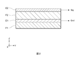
- FIG. 2 is a cross-sectional view taken along the line AA ′ of FIG.
- the vibration unit 120 is formed by laminating the lower electrode E1 (which is an example of a first electrode and a hafnium layer) on the substrate F1.
- a piezoelectric thin film F2 (a gallium nitride layer, which is an example of a piezoelectric layer) is laminated on the lower electrode E1 so as to cover the lower electrode E1, and the upper electrode is further formed on the piezoelectric thin film F2.
- E2 an example of the second electrode
- the substrate F1 is made of, for example, a degenerated n-type Si (silicon) semiconductor having a thickness of about 10 ⁇ m.
- a degenerated n-type Si (silicon) semiconductor having a thickness of about 10 ⁇ m.
- P phosphorus
- As arsenic
- Sb antimony
- the substrate F1 is preferably a substrate mainly containing degenerated Si, but is not limited to this.
- the substrate F1 may be formed from non-degenerate Si or a single crystal such as sapphire, or may be formed from an amorphous material such as glass or Si with an oxide film.
- the lower electrode E1 is formed of a hafnium layer mainly composed of a single metal of Hf (hafnium).
- the hafnium layer has a contact surface with the substrate F1 and a contact surface with the piezoelectric thin film F2.
- the upper electrode E2 is formed using, for example, Mo (molybdenum), Al (aluminum), Au (gold), W (tungsten), Pt (platinum), or the like.
- the piezoelectric thin film F2 is a piezoelectric thin film that contains GaN (gallium nitride) as a main component and converts an applied voltage into vibration.
- the piezoelectric thin film F2 expands and contracts in the in-plane direction of the XY plane according to the electric field applied to the piezoelectric thin film F2 by the lower electrode E1 and the upper electrode E2. Due to the expansion and contraction of the piezoelectric thin film F2, the vibration unit 120 undergoes contour vibration in the Y-axis direction.
- the stacked structure shown in FIG. 2 may be used for a semiconductor element.
- the stacked structure may be used as the piezoelectric thin film F2 in FIG. 2 as a semiconductor layer and the lower electrode E1 as an electrode or wiring layer connected to the semiconductor layer. Good.
- the lower electrode E1 and the piezoelectric thin film F2 are formed by sputtering.
- sputtering is performed on the substrate F1 under the following conditions to form the lower electrode E1.
- ⁇ Target Hf simple substance metal ⁇ Pressure 0.25Pa ⁇ Temperature 400 °C ⁇ Output 180W ⁇ Time 0.25 hours
- sputtering is performed on the formed lower electrode E1 under the following conditions to form a piezoelectric thin film F2.
- the upper electrode E2 is processed into a desired shape by etching or the like.
- the vibrating unit 120 forms the lower electrode E1 and the piezoelectric thin film F2 by sputtering. Therefore, since GaN can be formed at a low temperature, the lower electrode E1 can be formed by a simple apparatus or process.
- the lower electrode of the comparative example is formed using Ti (titanium), TiN (titanium nitride), and HfN (hafnium nitride).
- Ti titanium
- TiN titanium nitride
- HfN hafnium nitride
- FIG. 3A is a graph showing the result of rocking curve measurement performed on the GaN film formed on the lower electrode formed using Ti.
- FIG. 3B shows the result of rocking curve measurement when TiN is used for the lower electrode
- FIG. 3C shows the result of rocking curve measurement when HfN is used for the lower electrode.
- the full width at half maximum of the rocking curve is 10 degrees or more in any case.
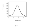
- FIG. 3D shows the result of rocking curve measurement performed on the piezoelectric thin film F2 according to this embodiment.
- the half width of the rocking curve of Hf (002) is about 2 deg.
- Hf as the lower electrode E1
- the crystallinity of the piezoelectric thin film F2 mainly formed of GaN formed on the lower electrode E1 can be enhanced.
- Hf has a hexagonal crystal structure, and the peak of Hf (002) is strongly observed by XRD (X-ray diffraction, X-ray diffraction).
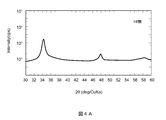
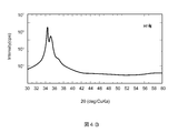
- FIG. 4A is a graph showing the results of X-ray diffraction performed on a comparative GaN film formed directly on the substrate without forming the lower electrode E1.
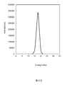
- FIG. 4B is a graph showing the results of X-ray diffraction performed on the piezoelectric thin film F2 according to this embodiment. 4A and 4B, the horizontal axis indicates the angle of the reflected wave with respect to the incident wave, and the vertical axis indicates the intensity of the reflected wave.
- the vibration part 120 according to the present embodiment includes the lower electrode E1 mainly composed of Hf, whereby the intensity of the diffraction peak is improved, and the crystallinity of the piezoelectric thin film F2 is increased. I understand that.
- the half value width in the rocking curve measurement of GaN (002) was 10.55 deg, and the average value of the piezoelectric constant was 0.83 pc / N.
- the full width at half maximum in the rocking curve measurement was about 2 deg, and the average value of the piezoelectric constant was 3.18 pc / N.
- GaN has a wurtzite structure, and the peak of GaN (002) is strongly observed by XRD.
- the vibration unit 120 forms a piezoelectric thin film F2 mainly composed of GaN on the lower electrode E1 mainly composed of Hf. It can be seen that the piezoelectric constant can be obtained.
- FIG. 5 is a diagram showing a laminated structure of the vibration unit 120 according to the present embodiment.
- the lower electrode E1 according to the present embodiment is mainly composed of a first layer E11 (which is an example of a first hafnium layer) that has a surface in contact with the substrate F1 as a main component of a single metal of Hf, and a single metal of Hf.
- a second layer E13 (which is an example of a second hafnium layer) having a surface in contact with the piezoelectric thin film F2 as a component, and an intermediate layer E12 (an aluminum layer) formed between the first layer and the second layer.
- the intermediate layer E12 is preferably a layer containing Al (aluminum) as a main component, but is not limited to this.
- Al aluminum
- an AlCu (aluminum-copper) alloy or Cu (copper) has a lower resistivity than Hf. It may be a metal layer.
- the first layer E11, the second layer E13, and the intermediate layer E12 are all preferably formed by sputtering.
- the film formation conditions for sputtering the first layer E11 and the second layer E13 are the same as the film formation conditions for the lower electrode E1 in the first embodiment.
- a vapor deposition method may be used.
- the vibration unit 120 according to the present embodiment can reduce the resistance value by including the intermediate layer E12 in the lower electrode E1. Therefore, a low-loss piezoelectric resonator can be manufactured by using the vibration unit 120 according to this embodiment.
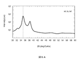
- FIG. 6A is a graph showing the results of X-ray diffraction performed on the piezoelectric thin film F2 according to this embodiment.
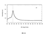
- FIG. 6B is a graph showing the results of X-ray diffraction performed on the piezoelectric thin film F2 according to the first embodiment.
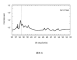
- FIG. 6C is a graph showing a result of X-ray diffraction performed on a GaN film as a comparative example in the case where the vibrating unit 120 has a configuration not including the first layer E11.
- the horizontal axis indicates the angle of the reflected wave with respect to the incident wave
- the vertical axis indicates the intensity of the reflected wave.
- the piezoelectric thin film F2 according to the present embodiment and the piezoelectric thin film F2 according to the first embodiment both have a maximum intensity of about 10 5 cps at the diffraction peak. Therefore, even when the vibration unit 120 includes the intermediate layer E12, it can be said that there is almost no influence on the crystallinity of the piezoelectric thin film F2.
- the intermediate layer E12 is formed directly on the substrate F1 without the first layer E11, so that the maximum intensity at the diffraction peak is about 10 3. It has dropped to cps. This is because when the intermediate layer E12 is directly formed on the substrate F1, the orientation of the intermediate layer E12 is deteriorated. As a result, the orientation of the second layer E13 and the GaN film formed on the intermediate layer E12 is reduced. This is thought to be because it gets worse.
- the vibration unit 120 includes the intermediate layer E12 between the first layer E11 and the second layer E13 formed from Hf, so that the crystallinity of the piezoelectric thin film F2 is not deteriorated.
- the resistance value of the lower electrode E1 can be lowered.
- the vibration unit 120 according to an embodiment of the present invention is provided between the substrate F1, the substrate F1, the piezoelectric thin film F2 mainly composed of gallium nitride, and the piezoelectric thin film F2 and the substrate F1.
- a lower electrode E1 that includes at least one hafnium layer mainly composed of a single metal of hafnium, and that is in contact with the piezoelectric thin film F2 in at least one hafnium layer. Accordingly, the vibration unit 120 according to an embodiment of the present invention can be formed by a simple process using a sputtering method.
- Hf has good lattice matching with GaN, which is the main reason why the vibration unit 120 can obtain good crystallinity and piezoelectricity. Further, as shown in FIG. 3, Hf was the best even when compared with a film mainly composed of TiN, Ti, or HfN having a small lattice mismatch like Hf.
- the closest atomic spacing is 3.2 ⁇ for GaN, 3.0 ⁇ for TiN, 3.0 for Ti, 3.2 H for HfN, and 3.2 H for Hf.
- the at least one hafnium layer is formed of a first layer E11 having a surface in contact with the substrate F1 and a second layer E13 having a surface in contact with the piezoelectric thin film F2, and the lower electrode E1 is formed by: It is preferable to further include an intermediate layer E12 formed mainly between aluminum and formed between the first layer E11 and the second layer E13. Since the lower electrode E1 includes the intermediate layer E12, the vibration unit 120 can reduce the resistance value.
- the vibration unit 120 further includes an upper electrode E2 provided to face the lower electrode E1 with the piezoelectric thin film F2 interposed therebetween.
- the resonator 10 according to an embodiment of the present invention can be formed by a simple process using a sputtering method by including the above-described vibrating portion 120.
- the piezoelectric element manufacturing method includes a step of forming a lower electrode E1 including a hafnium layer mainly composed of hafnium on a substrate F1 by sputtering, and nitriding the lower electrode E1. Forming a piezoelectric thin film F2 containing gallium as a main component by sputtering. Accordingly, since the piezoelectric thin film F2 containing GaN as a main component can be formed at a low temperature, the lower electrode E1 can be formed by a simple apparatus or process.
- each embodiment described above is for facilitating understanding of the present invention, and is not intended to limit the present invention.
- the present invention can be changed / improved without departing from the spirit thereof, and the present invention includes equivalents thereof.
- those obtained by appropriately modifying the design of each embodiment by those skilled in the art are also included in the scope of the present invention as long as they include the features of the present invention.
- each element included in each embodiment and its arrangement, material, condition, shape, size, and the like are not limited to those illustrated, and can be changed as appropriate.
- Each embodiment is an exemplification, and it is needless to say that a partial replacement or combination of configurations shown in different embodiments is possible, and these are also included in the scope of the present invention as long as they include the features of the present invention. .
Landscapes
- Engineering & Computer Science (AREA)
- Manufacturing & Machinery (AREA)
- Physics & Mathematics (AREA)
- Acoustics & Sound (AREA)
- Chemical & Material Sciences (AREA)
- Ceramic Engineering (AREA)
- Piezo-Electric Or Mechanical Vibrators, Or Delay Or Filter Circuits (AREA)
Abstract
GaNを圧電体として用いた窒化ガリウム構造体において、容易なプロセスで形成できる下部電極を提供することができる。 基板と、基板と対向して設けられ、窒化ガリウムを主成分とする窒化ガリウム層と、窒化ガリウム層と基板との間に設けられ、ハフニウムの単体金属を主成分とする少なくとも1層以上のハフニウム層を含み、少なくとも1層以上のハフニウム層において窒化ガリウム層と接触する第1電極と、を備える。
Description
本発明は、窒化ガリウム構造体、圧電素子、圧電素子の製造方法、及び圧電素子を用いた共振子に関する。
LED等の原料として用いられるGaN(窒化ガリウム)は、Q値が良好な圧電体である。GaN膜の成膜方法は、MOVPEやMBE、MPCVDのような手法が一般的である。これらの手法において、GaN膜の成膜温度は900℃以上であるため、GaN膜を圧電材料として用いた場合、基板とGaN膜との間に下部電極を形成することが非常に困難である。
非特許文献1には、GaN膜とSi基板との間に下部電極を形成する方法が開示されている。非特許文献1では、まずSi基板上にGaN膜を成膜させる。その後、成膜したGaN膜の一部をエッチング等によって除去して形成した孔に、W(タングステン)を充填し、さらに充填したWの上にSiO2を蒸着させ、その上に再度、GaN膜を形成する。
Azadeh Ansari, Che-Yu Liu, Chien-Chung Lin, Hao-Chung Kuo, Pei-Cheng Ku and Mina Rais-Zadeh, "GaN Micromechanical Resonators with Meshed Metal Bottom Electrode", Materials 2015, 8, p1204-1212
非特許文献1に記載の方法では、GaNの成膜にMOCVD法を用いており、その成膜温度は1070℃と高温である。また、非特許文献1の記載の方法で圧電素子を形成する場合、その製造プロセスが非常に複雑になる。
本発明はこのような事情に鑑みてなされたものであり、GaNを用いた窒化ガリウム構造体において、例えば成膜温度が600℃以下である容易なプロセスで形成できる下部電極を提供することを目的とする。
本発明の一側面に係る窒化ガリウム構造体は、基板と、基板と対向して設けられ、窒化ガリウムを主成分とする窒化ガリウム層と、窒化ガリウム層と基板との間に設けられ、ハフニウムの単体金属を主成分とする少なくとも1層以上のハフニウム層を含み、少なくとも1層以上のハフニウム層において窒化ガリウム層と接触する第1電極と、を備える。
本発明によれば、GaNを用いた窒化ガリウム構造体において、容易なプロセスで形成できる下部電極を提供することができる。
[第1の実施形態]
(1.共振子の構成)
以下、添付の図面を参照して本発明の第1実施形態について説明する。図1は、本発明の第1実施形態に係る窒化ガリウム構造体の一例である圧電素子を用いて形成した共振子10の一例を概略的に示す平面図である。共振子10は、MEMS技術を用いて製造されるMEMS振動子であり、図1の直交座標系におけるXY平面内で面内振動する。なお、本発明に係る圧電素子が用いられるのは図1に示される厚み広がり振動モードを用いた共振子に限定されず、厚み縦振動モード、ラム波振動モード、屈曲振動モード、表面波振動モードに用いられても良い。これらはタイミングデバイス、RFフィルタ、デュプレクサ、超音波トランスデューサーに応用される。さらに、アクチュエーター機能を持った圧電ミラーや圧電ジャイロ、圧力センサー機能を持った圧電マイクロフォンや超音波振動センサー等に用いられても良い。
(1.共振子の構成)
以下、添付の図面を参照して本発明の第1実施形態について説明する。図1は、本発明の第1実施形態に係る窒化ガリウム構造体の一例である圧電素子を用いて形成した共振子10の一例を概略的に示す平面図である。共振子10は、MEMS技術を用いて製造されるMEMS振動子であり、図1の直交座標系におけるXY平面内で面内振動する。なお、本発明に係る圧電素子が用いられるのは図1に示される厚み広がり振動モードを用いた共振子に限定されず、厚み縦振動モード、ラム波振動モード、屈曲振動モード、表面波振動モードに用いられても良い。これらはタイミングデバイス、RFフィルタ、デュプレクサ、超音波トランスデューサーに応用される。さらに、アクチュエーター機能を持った圧電ミラーや圧電ジャイロ、圧力センサー機能を持った圧電マイクロフォンや超音波振動センサー等に用いられても良い。
図1に示すように、共振子10は、振動部120(圧電素子の一例である。)と、保持部140と、保持腕110を備えている。
振動部120は、XY平面に沿って平面状に広がる板状の輪郭を有している。振動部120は、保持部140の内側に設けられており、振動部120と保持部140との間には、所定の間隔で空間が形成されている。
保持部140は、XY平面に沿って振動部120の外側を囲むように、矩形の枠状に形成される。例えば、保持部140は、角柱形状の枠体から一体に形成されている。なお、保持部140は、振動部120の周囲の少なくとも一部に設けられていればよく、枠状の形状に限定されない。
保持腕110は、保持部140の内側に設けられ、振動部120と保持部140とを接続する。
(2.振動部の積層構造)
次に、図2を用いて本実施形態に係る振動部120の積層構造について説明する。図2は、図1のAA´断面図である。
次に、図2を用いて本実施形態に係る振動部120の積層構造について説明する。図2は、図1のAA´断面図である。
本実施形態において、振動部120は、基板F1上に、下部電極E1(第1電極、及びハフニウム層の一例である。)が積層されて形成される。そして、下部電極E1の上には下部電極E1を覆うように圧電薄膜F2(窒化ガリウム層、圧電体層の一例である。)が積層されており、さらに圧電薄膜F2の上には、上部電極E2(第2電極の一例である。)が積層されている。
基板F1は、例えば、厚さ10μm程度の縮退したn形Si(シリコン)半導体から形成されている。n型ドーパントとしてP(リン)やAs(ヒ素)、Sb(アンチモン)などを含むことができる。なお、基板F1は縮退したSiを主成分とする基板であることが好ましいがこれに限定されない。例えば基板F1は、非縮退のSiや、サファイア等の単結晶から形成されてもよいし、ガラスや酸化膜付きのSiといった非晶質な材料から形成されても良い。
下部電極E1は、Hf(ハフニウム)の単体金属を主成分とするハフニウム層から形成される。ハフニウム層は、基板F1との接触面及び圧電薄膜F2との接触面を有している。
上部電極E2は、例えばMo(モリブデン)やAl(アルミニウム)、Au(金)、W(タングステン)、Pt(プラチナ)等を用いて形成される。
圧電薄膜F2は、GaN(窒化ガリウム)を主成分とし、印加された電圧を振動に変換する圧電体の薄膜である。圧電薄膜F2は、下部電極E1、上部電極E2によって圧電薄膜F2に印加される電界に応じて、XY平面の面内方向に伸縮する。この圧電薄膜F2の伸縮によって、振動部120は、Y軸方向に輪郭振動する。
なお、図2に示す積層構造は、半導体素子に用いられてもよい。当該積層構造は、例えば、トランジスタや発光素子などの半導体素子において、図2における圧電薄膜F2が半導体層として、また、下部電極E1が当該半導体層に接続される電極ないし配線層として用いられてもよい。
(3.成膜方法)
次に、本実施形態に係る、振動部120のうち、下部電極E1及び圧電薄膜F2の成膜方法について説明する。
本実施形態では、下部電極E1及び圧電薄膜F2は、スパッタ法によって成膜される。まず、基板F1上に以下の条件でスパッタリングを行い、下部電極E1を成膜する。
・ターゲット Hfの単体金属
・圧力 0.25Pa
・温度 400℃
・出力 180W
・時間 0.25時間
次に、本実施形態に係る、振動部120のうち、下部電極E1及び圧電薄膜F2の成膜方法について説明する。
本実施形態では、下部電極E1及び圧電薄膜F2は、スパッタ法によって成膜される。まず、基板F1上に以下の条件でスパッタリングを行い、下部電極E1を成膜する。
・ターゲット Hfの単体金属
・圧力 0.25Pa
・温度 400℃
・出力 180W
・時間 0.25時間
次に、形成された下部電極E1上に以下の条件でスパッタリングを行い、圧電薄膜F2を成膜する。
・ターゲット GaN焼結
・圧力 0.25Pa
・温度 500℃
・窒素濃度 50%(Ar:N2=1:1)
・出力 100W
・時間 3時間
圧電薄膜F2上に上部電極E2を形成した後、上部電極E2をエッチング等によって所望の形状に加工する。
・ターゲット GaN焼結
・圧力 0.25Pa
・温度 500℃
・窒素濃度 50%(Ar:N2=1:1)
・出力 100W
・時間 3時間
圧電薄膜F2上に上部電極E2を形成した後、上部電極E2をエッチング等によって所望の形状に加工する。
以上のように、本実施形態に係る振動部120は、下部電極E1と圧電薄膜F2とをスパッタリングによって成膜する。従って、GaNを低温で成膜することが可能になるため、下部電極E1を簡易な装置ないしプロセスによって形成することができる。
(4.比較例)
図3を参照し、本実施形態に係る下部電極E1上に形成した圧電薄膜F2の配向性と、比較例の下部電極上に形成したGaN膜の配向性とを、X線回折によって検証した結果を説明する。比較例の下部電極は、Ti(チタン)、TiN(窒化チタン)、HfN(窒化ハフニウム)をそれぞれ用いて形成したものである。図3A~3Dにおいて、横軸は反射面に対する入射波の角度を示し、縦軸は反射波の強度を示している。
図3を参照し、本実施形態に係る下部電極E1上に形成した圧電薄膜F2の配向性と、比較例の下部電極上に形成したGaN膜の配向性とを、X線回折によって検証した結果を説明する。比較例の下部電極は、Ti(チタン)、TiN(窒化チタン)、HfN(窒化ハフニウム)をそれぞれ用いて形成したものである。図3A~3Dにおいて、横軸は反射面に対する入射波の角度を示し、縦軸は反射波の強度を示している。
図3Aは、Tiを用いて形成した下部電極上に形成したGaN膜に対して、ロッキングカーブ測定を行った結果を示すグラフである。同様に、図3Bは下部電極にTiNを用いた場合、図3Cは下部電極にHfNを用いた場合におけるロッキングカーブ測定の結果を示している。図3A~3Cから明らかなように、いずれの場合もロッキングカーブの半値幅は10deg以上である。
他方で、図3Dは本実施形態に係る圧電薄膜F2に対してロッキングカーブ測定を行った結果を示している。この場合、Hf(002)のロッキングカーブの半値幅は2deg程度である。このように本実施形態によれば、下部電極E1としてHfを用いることで、下部電極E1上に形成される、GaNを主成分とする圧電薄膜F2の結晶性を高めることができる。なお、Hfは六方晶構造をとり、Hf(002)のピークがXRD(X―ray diffraction、X線回折)で強く観測される。
次に、図4を参照して、振動部120がHfを主成分とする下部電極E1を備えることの効果を検証した結果をさらに説明する。
図4Aは、下部電極E1を形成せずに基板上に直接形成した比較例のGaN膜に対してX線回折を行った結果を示すグラフである。また、図4Bは本実施形態に係る圧電薄膜F2に対してX線回折を行った結果)を示すグラフである。図4A、4Bにおいて、横軸は入射波に対する反射波の角度を示し、縦軸は反射波の強度を示している。
図4A及び4Bから明らかなように、比較例、すなわち、下部電極を有さないGaN膜における回折ピークの最大強度が1129cpsであるのに対して、本実施形態に係る圧電薄膜F2における回折ピークの最大強度は、276396cpsである。従って図4のグラフから、本実施形態に係る振動部120はHfを主成分とする下部電極E1を備えることによって、回折ピークの強度が向上することから、圧電薄膜F2の結晶性が高まっていることが分かる。
さらに、比較例のGaN膜では、GaN(002)のロッキングカーブ測定における半値幅は10.55deg、圧電定数の平均値は0.83pc/Nであった。他方で本実施形態に係る圧電薄膜F2においては、ロッキングカーブ測定における半値幅は2deg程度、圧電定数の平均値は3.18pc/Nであった。なお、GaNはウルツ鉱型構造をとり、GaN(002)のピークがXRDで強く観測される。
これらの結果から、本実施形態に係る振動部120はHfを主成分とする下部電極E1の上に、GaNを主成分とする圧電薄膜F2を形成することによって、良好な結晶性と、良好な圧電定数を得られることが分かる。
[第2の実施形態]
第2の実施形態以降では第1の実施形態と共通の事柄についての記述を省略し、異なる点についてのみ説明する。特に、同様の構成による同様の作用効果については実施形態毎には逐次言及しない。
第2の実施形態以降では第1の実施形態と共通の事柄についての記述を省略し、異なる点についてのみ説明する。特に、同様の構成による同様の作用効果については実施形態毎には逐次言及しない。
図5は、本実施形態に係る振動部120の積層構造を示す図である。本実施形態に係る下部電極E1は、Hfの単体金属を主成分とし、基板F1と接触する面を有する第1層E11(第1ハフニウム層の一例である。)と、Hfの単体金属を主成分とし、圧電薄膜F2と接触する面を有する第2層E13(第2ハフニウム層の一例である。)と、第1層と第2層との間に形成された中間層E12(アルミニウム層の一例である。)とから形成される。なお、中間層E12はAl(アルミニウム)を主成分とする層であることが好ましいがこれに限定されず、例えばAlCu(アルミニウム-銅)合金やCu(銅)等、Hfよりも低い抵抗率を持つ金属層であってもよい。
第1層E11、第2層E13、及び中間層E12はいずれもスパッタ法によって形成されることが好ましい。なお、第1層E11、及び第2層E13のスパッタリングにおける成膜条件は、第1実施形態における下部電極E1の成膜条件と同一である。他の成膜方法として、蒸着法で形成しても良い。
本実施形態に係る振動部120は、下部電極E1に中間層E12を備えることによって、抵抗値を下げることができる。従って本実施形態に係る振動部120を用いることで、低損失な圧電共振子を製造することが可能になる。
次に、図6を用いて本実施形態に係る振動部120が、中間層E12を有することによる圧電薄膜F2の結晶性への影響について説明する。図6Aは、本実施形態に係る圧電薄膜F2に対してX線回折を行った結果を示すグラフである。図6Bは第1実施形態に係る圧電薄膜F2に対してX線回折を行った結果を示すグラフである。図6Cは比較例として、振動部120が第1層E11を備えない構成である場合のGaN膜に対してX線回折を行った結果を示すグラフである。図6A~6Cにおいて、横軸は入射波に対する反射波の角度を示し、縦軸は反射波の強度を示している。
図6A、6Bの結果から明らかなように、本実施形態に係る圧電薄膜F2と第1実施形態に係る圧電薄膜F2とでは、回折ピークにおける最大強度はいずれも約105cpsを示している。従って、振動部120が中間層E12を備えた場合でも、圧電薄膜F2の結晶性への影響はほとんどないといえる。
他方で、図6Cの結果から、比較例のGaN膜では、第1層E11を備えずに、基板F1上に直接、中間層E12が形成されることによって、回折ピークにおける最大強度は約103cpsまで低下している。これは、基板F1に直接中間層E12を形成した場合には、中間層E12の配向性が悪くなるため、その結果、中間層E12上に形成される第2層E13及びGaN膜の配向性が悪くなってしまうためであると考えられる。
以上のように、本実施形態に係る振動部120は、Hfから形成される第1層E11、第2層E13の間に中間層E12を備えることで、圧電薄膜F2の結晶性を劣化させずに、下部電極E1の抵抗値を下げることができる。
以上、本発明の例示的な実施形態について説明した。本発明の一実施形態に係る振動部120は、基板F1と、基板F1と対向して設けられ、窒化ガリウムを主成分とする圧電薄膜F2と、圧電薄膜F2と基板F1との間に設けられ、ハフニウムの単体金属を主成分とする少なくとも1層以上のハフニウム層を含み、少なくとも1層以上のハフニウム層において、圧電薄膜F2と接触する下部電極E1を備える。これによって本発明の一実施形態に係る振動部120は、スパッタ法を用いて簡易なプロセスで形成することができる。HfはGaNとの格子整合が良いことが、振動部120が良好な結晶性と圧電性を得ることができる主な理由と考えられる。また、図3に示したように、Hfと同様に格子のミスマッチが小さいTiN、Ti又はHfNを主成分とする膜と比較しても、Hfが最も良好であった。なお、最近接原子間隔は、GaNが3.2Å、TiNが3.0Å、 Tiが3.0Å、HfNが3.2Å、Hfが3.2Åである。
さらに、上述の少なくとも1層以上のハフニウム層は、基板F1と接触する面を有する第1層E11と、圧電薄膜F2と接触する面を有する第2層E13とから形成され、下部電極E1は、第1層E11と第2層E13との間に形成された、アルミニウムを主成分とする中間層E12をさらに有することが好ましい。下部電極E1が中間層E12を備えることによって、振動部120は抵抗値を下げることができる。
また、振動部120は、圧電薄膜F2を挟んで下部電極E1と対向して設けられた上部電極E2をさらに備えることが好ましい。
さらに本発明の一実施形態に係る共振子10は、上述の振動部120を備えることによって、スパッタ法を用いて簡易なプロセスで形成することができる。
また、本発明の一実施形態に係る圧電素子製造方法は、基板F1の上に、ハフニウムを主成分とするハフニウム層を含む下部電極E1をスパッタリングによって形成する工程と、下部電極E1の上に窒化ガリウムを主成分とする圧電薄膜F2をスパッタリングによって形成する工程と、を含む。これによって、GaNを主成分とする圧電薄膜F2を低温で成膜することができるため、下部電極E1を簡易な装置ないしプロセスによって形成することができる。
なお、以上説明した各実施形態は、本発明の理解を容易にするためのものであり、本発明を限定して解釈するためのものではない。本発明は、その趣旨を逸脱することなく、変更/改良され得るととともに、本発明にはその等価物も含まれる。即ち、各実施形態に当業者が適宜設計変更を加えたものも、本発明の特徴を備えている限り、本発明の範囲に包含される。例えば、各実施形態が備える各要素およびその配置、材料、条件、形状、サイズなどは、例示したものに限定されるわけではなく適宜変更することができる。また、各実施形態は例示であり、異なる実施形態で示した構成の部分的な置換または組み合わせが可能であることは言うまでもなく、これらも本発明の特徴を含む限り本発明の範囲に包含される。
10 共振子
120 振動部
F1 基板
F2 圧電薄膜
E1 下部電極
E11 第1層
E12 中間層
E13 第2層
E2 上部電極
120 振動部
F1 基板
F2 圧電薄膜
E1 下部電極
E11 第1層
E12 中間層
E13 第2層
E2 上部電極
Claims (6)
- 基板と、
前記基板と対向して設けられ、窒化ガリウムを主成分とする窒化ガリウム層と、
前記窒化ガリウム層と前記基板との間に設けられ、ハフニウムを主成分とする少なくとも1層以上のハフニウム層を含み、前記少なくとも1層以上のハフニウム層において前記窒化ガリウム層と接触する第1電極と、
を備える窒化ガリウム構造体。 - 請求項1に記載の窒化ガリウム構造体を備える圧電素子。
- 前記少なくとも1層以上のハフニウム層は、
前記基板と接触する第1ハフニウム層と、前記窒化ガリウム層と接触する第2ハフニウム層と、を含み、
前記第1電極は、
前記第1ハフニウム層と前記第2ハフニウム層との間に形成された、アルミニウムを主成分とするアルミニウム層をさらに有する、請求項2に記載の圧電素子。 - 前記窒化ガリウム層を挟んで前記第1電極と対向して設けられた第2電極をさらに備える、請求項2または3に記載の圧電素子。
- 請求項2~4いずれか一項記載の圧電素子を備える共振子。
- 基板の上に、ハフニウムを主成分とするハフニウム層を含む電極をスパッタリングによって形成する工程と、
前記電極の上に窒化ガリウムを主成分とする圧電体層をスパッタリングによって形成する工程と、
を含む圧電素子製造方法。
Priority Applications (2)
| Application Number | Priority Date | Filing Date | Title |
|---|---|---|---|
| JP2018504584A JP6666994B2 (ja) | 2016-03-11 | 2017-03-09 | 圧電素子、及び圧電素子の製造方法 |
| US16/126,248 US11451211B2 (en) | 2016-03-11 | 2018-09-10 | Gallium nitride structure, piezoelectric element, method of manufacturing piezoelectric element, and resonator using piezoelectric element |
Applications Claiming Priority (2)
| Application Number | Priority Date | Filing Date | Title |
|---|---|---|---|
| JP2016048236 | 2016-03-11 | ||
| JP2016-048236 | 2016-03-11 |
Related Child Applications (1)
| Application Number | Title | Priority Date | Filing Date |
|---|---|---|---|
| US16/126,248 Continuation US11451211B2 (en) | 2016-03-11 | 2018-09-10 | Gallium nitride structure, piezoelectric element, method of manufacturing piezoelectric element, and resonator using piezoelectric element |
Publications (1)
| Publication Number | Publication Date |
|---|---|
| WO2017155032A1 true WO2017155032A1 (ja) | 2017-09-14 |
Family
ID=59790561
Family Applications (1)
| Application Number | Title | Priority Date | Filing Date |
|---|---|---|---|
| PCT/JP2017/009459 Ceased WO2017155032A1 (ja) | 2016-03-11 | 2017-03-09 | 窒化ガリウム構造体、圧電素子、圧電素子の製造方法、及び圧電素子を用いた共振子 |
Country Status (3)
| Country | Link |
|---|---|
| US (1) | US11451211B2 (ja) |
| JP (1) | JP6666994B2 (ja) |
| WO (1) | WO2017155032A1 (ja) |
Citations (2)
| Publication number | Priority date | Publication date | Assignee | Title |
|---|---|---|---|---|
| JP2004269313A (ja) * | 2003-03-07 | 2004-09-30 | Hitachi Cable Ltd | 窒化ガリウム結晶基板の製造方法 |
| JP2005136115A (ja) * | 2003-10-30 | 2005-05-26 | Tdk Corp | 電子デバイス及びその製造方法 |
Family Cites Families (7)
| Publication number | Priority date | Publication date | Assignee | Title |
|---|---|---|---|---|
| US7388318B2 (en) * | 2002-06-20 | 2008-06-17 | Ube Industries, Ltd. | Thin film piezoelectric resonator, thin film piezoelectric device, and manufacturing method thereof |
| JP5073772B2 (ja) * | 2009-09-16 | 2012-11-14 | 日本電波工業株式会社 | 圧電デバイス |
| KR101712094B1 (ko) * | 2009-11-27 | 2017-03-03 | 포항공과대학교 산학협력단 | 질화물갈륨계 수직 발광다이오드 및 그 제조 방법 |
| WO2011146015A1 (en) * | 2010-05-18 | 2011-11-24 | Agency For Science, Technology And Research | Method of forming a light emitting diode structure and a light emitting diode structure |
| JP6205871B2 (ja) * | 2013-06-05 | 2017-10-04 | ソニー株式会社 | 磁気記録媒体 |
| US9929279B2 (en) * | 2014-02-05 | 2018-03-27 | Semiconductor Energy Laboratory Co., Ltd. | Semiconductor device and manufacturing method thereof |
| US10340885B2 (en) * | 2014-05-08 | 2019-07-02 | Avago Technologies International Sales Pte. Limited | Bulk acoustic wave devices with temperature-compensating niobium alloy electrodes |
-
2017
- 2017-03-09 WO PCT/JP2017/009459 patent/WO2017155032A1/ja not_active Ceased
- 2017-03-09 JP JP2018504584A patent/JP6666994B2/ja active Active
-
2018
- 2018-09-10 US US16/126,248 patent/US11451211B2/en active Active
Patent Citations (2)
| Publication number | Priority date | Publication date | Assignee | Title |
|---|---|---|---|---|
| JP2004269313A (ja) * | 2003-03-07 | 2004-09-30 | Hitachi Cable Ltd | 窒化ガリウム結晶基板の製造方法 |
| JP2005136115A (ja) * | 2003-10-30 | 2005-05-26 | Tdk Corp | 電子デバイス及びその製造方法 |
Also Published As
| Publication number | Publication date |
|---|---|
| JP6666994B2 (ja) | 2020-03-18 |
| JPWO2017155032A1 (ja) | 2018-12-20 |
| US20190007026A1 (en) | 2019-01-03 |
| US11451211B2 (en) | 2022-09-20 |
Similar Documents
| Publication | Publication Date | Title |
|---|---|---|
| US11495726B2 (en) | Piezoelectric element, and resonator using piezoelectric element | |
| US11629046B2 (en) | MEMS device | |
| CN111244263B (zh) | 压电薄膜元件 | |
| KR101386754B1 (ko) | 탄성파 소자 | |
| CN107112977B (zh) | 压电膜以及压电振子 | |
| US7489067B2 (en) | Component with a piezoelectric functional layer | |
| US9862592B2 (en) | MEMS transducer and method for manufacturing the same | |
| US11753296B2 (en) | MEMS device and method for manufacturing mems device | |
| JP7269719B2 (ja) | 圧電膜およびその製造方法、圧電デバイス、共振器、フィルタ並びにマルチプレクサ | |
| US11909379B2 (en) | MEMS device having a connection portion formed of a eutectic alloy | |
| JP6225544B2 (ja) | 圧電素子の製造方法 | |
| JP2005136534A (ja) | 薄膜バルク波共振器 | |
| JP2005136115A (ja) | 電子デバイス及びその製造方法 | |
| US9071222B2 (en) | Method for forming an electrode | |
| US20220368301A1 (en) | Method of manufacturing collective substrate and collective substrate | |
| JP6698159B2 (ja) | 圧電膜及びその製造方法並びに圧電膜を用いた圧電部品 | |
| JP6666994B2 (ja) | 圧電素子、及び圧電素子の製造方法 | |
| US20210371273A1 (en) | Resonance device and resonance device manufacturing method | |
| WO2017149675A1 (ja) | 圧電膜、その製造方法、及び圧電膜を用いた圧電部品 | |
| JP6998718B2 (ja) | 圧電素子、圧電素子の製造方法、及び圧電素子を用いた共振子 | |
| JP2009231615A (ja) | 圧電素子の製造方法、圧電素子、電子機器 | |
| JP2018056349A (ja) | 圧電膜及びその製造方法並びに圧電膜を用いた圧電部品 | |
| CN118830346A (zh) | 膜构造体以及电子器件 | |
| KR20200113508A (ko) | 고순도 AlxGa1-xN (0.5≤x≤1) 압전 박막을 제조하는 방법 및 이 박막을 이용하는 장치 |
Legal Events
| Date | Code | Title | Description |
|---|---|---|---|
| WWE | Wipo information: entry into national phase |
Ref document number: 2018504584 Country of ref document: JP |
|
| NENP | Non-entry into the national phase |
Ref country code: DE |
|
| 121 | Ep: the epo has been informed by wipo that ep was designated in this application |
Ref document number: 17763372 Country of ref document: EP Kind code of ref document: A1 |
|
| 122 | Ep: pct application non-entry in european phase |
Ref document number: 17763372 Country of ref document: EP Kind code of ref document: A1 |