WO2017154195A1 - 半導体装置 - Google Patents
半導体装置 Download PDFInfo
- Publication number
- WO2017154195A1 WO2017154195A1 PCT/JP2016/057749 JP2016057749W WO2017154195A1 WO 2017154195 A1 WO2017154195 A1 WO 2017154195A1 JP 2016057749 W JP2016057749 W JP 2016057749W WO 2017154195 A1 WO2017154195 A1 WO 2017154195A1
- Authority
- WO
- WIPO (PCT)
- Prior art keywords
- wiring board
- output
- ground
- terminal
- semiconductor device
- Prior art date
- Legal status (The legal status is an assumption and is not a legal conclusion. Google has not performed a legal analysis and makes no representation as to the accuracy of the status listed.)
- Ceased
Links
Images



Classifications
-
- H—ELECTRICITY
- H10—SEMICONDUCTOR DEVICES; ELECTRIC SOLID-STATE DEVICES NOT OTHERWISE PROVIDED FOR
- H10W—GENERIC PACKAGES, INTERCONNECTIONS, CONNECTORS OR OTHER CONSTRUCTIONAL DETAILS OF DEVICES COVERED BY CLASS H10
- H10W72/00—Interconnections or connectors in packages
-
- H—ELECTRICITY
- H10—SEMICONDUCTOR DEVICES; ELECTRIC SOLID-STATE DEVICES NOT OTHERWISE PROVIDED FOR
- H10W—GENERIC PACKAGES, INTERCONNECTIONS, CONNECTORS OR OTHER CONSTRUCTIONAL DETAILS OF DEVICES COVERED BY CLASS H10
- H10W20/00—Interconnections in chips, wafers or substrates
- H10W20/40—Interconnections external to wafers or substrates, e.g. back-end-of-line [BEOL] metallisations or vias connecting to gate electrodes
- H10W20/41—Interconnections external to wafers or substrates, e.g. back-end-of-line [BEOL] metallisations or vias connecting to gate electrodes characterised by their conductive parts
- H10W20/427—Power or ground buses
-
- H—ELECTRICITY
- H10—SEMICONDUCTOR DEVICES; ELECTRIC SOLID-STATE DEVICES NOT OTHERWISE PROVIDED FOR
- H10W—GENERIC PACKAGES, INTERCONNECTIONS, CONNECTORS OR OTHER CONSTRUCTIONAL DETAILS OF DEVICES COVERED BY CLASS H10
- H10W70/00—Package substrates; Interposers; Redistribution layers [RDL]
- H10W70/40—Leadframes
- H10W70/421—Shapes or dispositions
-
- H—ELECTRICITY
- H10—SEMICONDUCTOR DEVICES; ELECTRIC SOLID-STATE DEVICES NOT OTHERWISE PROVIDED FOR
- H10W—GENERIC PACKAGES, INTERCONNECTIONS, CONNECTORS OR OTHER CONSTRUCTIONAL DETAILS OF DEVICES COVERED BY CLASS H10
- H10W70/00—Package substrates; Interposers; Redistribution layers [RDL]
- H10W70/40—Leadframes
- H10W70/481—Leadframes for devices being provided for in groups H10D8/00 - H10D48/00
-
- H—ELECTRICITY
- H10—SEMICONDUCTOR DEVICES; ELECTRIC SOLID-STATE DEVICES NOT OTHERWISE PROVIDED FOR
- H10W—GENERIC PACKAGES, INTERCONNECTIONS, CONNECTORS OR OTHER CONSTRUCTIONAL DETAILS OF DEVICES COVERED BY CLASS H10
- H10W90/00—Package configurations
-
- H—ELECTRICITY
- H10—SEMICONDUCTOR DEVICES; ELECTRIC SOLID-STATE DEVICES NOT OTHERWISE PROVIDED FOR
- H10W—GENERIC PACKAGES, INTERCONNECTIONS, CONNECTORS OR OTHER CONSTRUCTIONAL DETAILS OF DEVICES COVERED BY CLASS H10
- H10W90/00—Package configurations
- H10W90/811—Multiple chips on leadframes
-
- H—ELECTRICITY
- H10—SEMICONDUCTOR DEVICES; ELECTRIC SOLID-STATE DEVICES NOT OTHERWISE PROVIDED FOR
- H10W—GENERIC PACKAGES, INTERCONNECTIONS, CONNECTORS OR OTHER CONSTRUCTIONAL DETAILS OF DEVICES COVERED BY CLASS H10
- H10W70/00—Package substrates; Interposers; Redistribution layers [RDL]
- H10W70/40—Leadframes
- H10W70/464—Additional interconnections in combination with leadframes
- H10W70/465—Bumps or wires
-
- H—ELECTRICITY
- H10—SEMICONDUCTOR DEVICES; ELECTRIC SOLID-STATE DEVICES NOT OTHERWISE PROVIDED FOR
- H10W—GENERIC PACKAGES, INTERCONNECTIONS, CONNECTORS OR OTHER CONSTRUCTIONAL DETAILS OF DEVICES COVERED BY CLASS H10
- H10W70/00—Package substrates; Interposers; Redistribution layers [RDL]
- H10W70/40—Leadframes
- H10W70/464—Additional interconnections in combination with leadframes
- H10W70/466—Tape carriers or flat leads
-
- H—ELECTRICITY
- H10—SEMICONDUCTOR DEVICES; ELECTRIC SOLID-STATE DEVICES NOT OTHERWISE PROVIDED FOR
- H10W—GENERIC PACKAGES, INTERCONNECTIONS, CONNECTORS OR OTHER CONSTRUCTIONAL DETAILS OF DEVICES COVERED BY CLASS H10
- H10W72/00—Interconnections or connectors in packages
- H10W72/071—Connecting or disconnecting
- H10W72/075—Connecting or disconnecting of bond wires
- H10W72/07551—Connecting or disconnecting of bond wires characterised by changes in properties of the bond wires during the connecting
- H10W72/07552—Connecting or disconnecting of bond wires characterised by changes in properties of the bond wires during the connecting changes in structures or sizes
-
- H—ELECTRICITY
- H10—SEMICONDUCTOR DEVICES; ELECTRIC SOLID-STATE DEVICES NOT OTHERWISE PROVIDED FOR
- H10W—GENERIC PACKAGES, INTERCONNECTIONS, CONNECTORS OR OTHER CONSTRUCTIONAL DETAILS OF DEVICES COVERED BY CLASS H10
- H10W72/00—Interconnections or connectors in packages
- H10W72/50—Bond wires
- H10W72/521—Structures or relative sizes of bond wires
- H10W72/527—Multiple bond wires having different sizes
-
- H—ELECTRICITY
- H10—SEMICONDUCTOR DEVICES; ELECTRIC SOLID-STATE DEVICES NOT OTHERWISE PROVIDED FOR
- H10W—GENERIC PACKAGES, INTERCONNECTIONS, CONNECTORS OR OTHER CONSTRUCTIONAL DETAILS OF DEVICES COVERED BY CLASS H10
- H10W72/00—Interconnections or connectors in packages
- H10W72/90—Bond pads, in general
- H10W72/921—Structures or relative sizes of bond pads
- H10W72/926—Multiple bond pads having different sizes
-
- H—ELECTRICITY
- H10—SEMICONDUCTOR DEVICES; ELECTRIC SOLID-STATE DEVICES NOT OTHERWISE PROVIDED FOR
- H10W—GENERIC PACKAGES, INTERCONNECTIONS, CONNECTORS OR OTHER CONSTRUCTIONAL DETAILS OF DEVICES COVERED BY CLASS H10
- H10W90/00—Package configurations
- H10W90/701—Package configurations characterised by the relative positions of pads or connectors relative to package parts
- H10W90/751—Package configurations characterised by the relative positions of pads or connectors relative to package parts of bond wires
- H10W90/756—Package configurations characterised by the relative positions of pads or connectors relative to package parts of bond wires between a chip and a stacked lead frame, conducting package substrate or heat sink
-
- H—ELECTRICITY
- H10—SEMICONDUCTOR DEVICES; ELECTRIC SOLID-STATE DEVICES NOT OTHERWISE PROVIDED FOR
- H10W—GENERIC PACKAGES, INTERCONNECTIONS, CONNECTORS OR OTHER CONSTRUCTIONAL DETAILS OF DEVICES COVERED BY CLASS H10
- H10W90/00—Package configurations
- H10W90/701—Package configurations characterised by the relative positions of pads or connectors relative to package parts
- H10W90/761—Package configurations characterised by the relative positions of pads or connectors relative to package parts of strap connectors
- H10W90/766—Package configurations characterised by the relative positions of pads or connectors relative to package parts of strap connectors between a chip and a stacked lead frame, conducting package substrate or heat sink
Definitions
- the present invention relates to a semiconductor device.
- the semiconductor device 200 includes power supply terminals 201 and 205, output terminals 202, 204 and 206, and ground terminals 203 and 207.
- these three types of terminals protrude in the same direction from the sealing resin 230 of the device main body 220.
- the gate terminals 208 to 213 protrude from the sealing resin 230 of the apparatus main body 220 in the opposite direction to the above three types of terminals (for example, Patent Document 1).
- the semiconductor device 200 includes a first current path 301 through which a current flows from the power supply terminal 201 through the circuit of the apparatus main body 220 to the output terminal 202, and a second current path 302 through which a current flows between the output terminal 202 and the ground terminal 203. And have.
- the semiconductor device 200 includes a first current path 303 in which current flows from the power supply terminal 205 to the output terminal 204 through the circuit of the apparatus main body 220, and a second current path 304 in which current flows between the output terminal 204 and the ground terminal 203.
- the semiconductor device 200 includes a first current path 305 in which a current flows from the power supply terminal 205 through the circuit of the apparatus main body 220 to the output terminal 206, and a second current path 306 in which a current flows between the output terminal 206 and the ground terminal 207.
- the first current path 301 has a folded portion 301A for changing the direction in which the current flows.
- the second current path 302 has a folded portion 302A for changing the direction in which the current flows.
- each current path becomes long. Further, a place for providing the folded portions 301A and 302A in the apparatus main body 220 is required. Therefore, the dimensions of the semiconductor device 200, particularly the dimensions in the terminal arrangement direction (left and right direction in FIG. 5), become large, and it may be difficult to reduce the size of the semiconductor device 200.
- the present invention has been made to solve the above problems, and an object of the present invention is to provide a semiconductor device capable of reducing the length of the current path and reducing the size.
- one embodiment of the present invention includes at least one circuit unit including a device main body, a power supply terminal protruding from the device main body, an output terminal, and a ground terminal, and the output terminal and the A ground terminal protrudes in opposite directions with respect to the device body, and the power supply terminal protrudes in the same direction as the ground terminal and is shifted in a direction perpendicular to the arrangement direction of the output terminal and the ground terminal. It is a semiconductor device located.
- the output terminal and the ground terminal protrude in opposite directions with respect to the device body, the power supply terminal protrudes in the same direction as the ground terminal, and the arrangement of the output terminal and the ground terminal Since the position is shifted in the direction orthogonal to the direction, the conventional folded portion does not appear in the current path. Thereby, the length of the current path can be shortened. In addition, the size of the semiconductor device can be reduced.
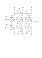
- FIG. 3 is a plan configuration diagram illustrating an example of a semiconductor device according to the present embodiment.
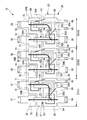
- FIG. 4 is an example of a circuit diagram in the semiconductor device according to the present embodiment. It is a plane block diagram which shows the other example of the semiconductor device by this embodiment. It is another example of the circuit diagram in the semiconductor device by this embodiment. It is a plane block diagram which shows an example of the conventional semiconductor device.
- the semiconductor device 10 includes a device main body 20, power terminals 31, 32, 33 projecting from the device main body 20, output terminals 34, 35, 36, and ground terminals 37, 38, 39. Are provided with circuit units 41, 42, and 43, respectively.
- the device main body 20 is formed by integrating device units 21, 22, and 23 corresponding to the circuit units 41, 42, and 43, respectively.
- the circuit units 41, 42, 43 are arranged in this order along the longitudinal direction of the semiconductor device 10 (left-right direction in FIG. 1).
- the first circuit unit 41 includes a first device unit 21, a first power supply terminal 31 that protrudes from the first device unit 21, a first output terminal 34, and a first ground terminal 37.
- the second circuit unit 42 includes a second device unit 22, a second power supply terminal 32, a second output terminal 35, and a second ground terminal 38 protruding from the second device unit 22.
- the third circuit unit 43 includes a third device unit 23 and a third power supply terminal 33, a third output terminal 36, and a third ground terminal 39 protruding from the third device unit 23.
- the first circuit unit 41, the second circuit unit 42, and the third circuit unit 43 have substantially the same shape when seen in a plan view.
- the apparatus body 20 may include a sealing resin 50 that covers the circuit units 41, 42, and 43. In that case, the power supply terminals 31, 32, 33, the output terminals 34, 35, 36 and the ground terminals 37, 38, 39 protrude from the sealing resin 50.
- the output terminals 34, 35, 36 and the ground terminals 37, 38, 39 protrude in opposite directions with respect to the apparatus main body 20.
- the output terminals 34, 35, 36 and the ground terminals 37, 38, 39 protrude from the side surface along the longitudinal direction of the apparatus body 20 perpendicularly to the side surface and opposite to each other.
- the power terminals 31, 32, 33 protrude in the same direction as the ground terminals 37, 38, 39.
- the power supply terminals 31, 32, and 33 are shifted from each other in a direction orthogonal to the arrangement direction of the output terminals 34, 35, and 36 and the ground terminals 37, 38, and 39.
- the arrangement direction of the output terminals 34, 35, 36 and the ground terminals 37, 38, 39 is a direction from the first output terminal 34 toward the first ground terminal 37 and a direction from the second output terminal 35 toward the second ground terminal 38. And the direction from the third output terminal 36 to the third ground terminal 39. That is, the power supply terminals 31, 32, 33 are located in a direction perpendicular to the arrangement direction of the output terminals 34, 35, 36 and the ground terminals 37, 38, 39. This means that they are not on a straight line connecting the terminals 34, 35, 36 and the ground terminals 37, 38, 39.
- the circuit units 41, 42, and 43 may have gate terminals 61 to 66 protruding from the device main body 20 (device units 21, 22, and 23).
- the power supply terminals 31, 32 and 33 and the gate terminals 61 to 66 protrude in opposite directions with respect to the apparatus main body 20.
- the power supply terminals 31, 32, 33 and the gate terminals 61 to 66 protrude from the side surface along the longitudinal direction of the apparatus body 20 in the opposite directions perpendicular to the side surface.
- the gate terminals 61 to 66 protrude from the sealing resin 50.
- the widths of the power terminals 31, 32, 33, the output terminals 34, 35, 36 and the ground terminals 37, 38, 39 are preferably larger than the widths of the gate terminals 61-66.
- the length of the first current path 71, the length of the first current path 73, and the length of the first current path 75 correspond to each other that the lengths of these three current paths are equal to each other, This means that the difference in path length is very small.
- the length of the second current path 72, the length of the second current path 74, and the length of the second current path 76 correspond to each other that the lengths of these three current paths are equal to each other, This means that the difference in path length is very small.
- the apparatus body 20 includes a power supply wiring board 24 common to the three apparatus units 21, 22, 23, ground wiring boards 25, 26, 27 provided individually in the apparatus units 21, 22, and 23, and an apparatus unit 21. , 22 and 23, respectively, output wiring boards 28, 29 and 30 provided individually.
- the power supply wiring board 24, the ground wiring boards 25, 26, and 27 and the output wiring boards 28, 29, and 30 are arranged with a space therebetween.
- the power wiring board 24 extends in the longitudinal direction of the apparatus main body 20. When viewed in plan, the power supply wiring board 24 has a periodic uneven shape along its longitudinal direction.
- the power supply wiring board 24 includes three narrow portions 24A and three wide portions 24B that are continuous in a direction orthogonal to the arrangement direction of the output terminals 34, 35, 36 and the ground terminals 37, 38, 39.
- the narrow portion 24A is narrow in the arrangement direction of the output terminals 34, 35, 36 and the ground terminals 37, 38, 39.
- the wide portion 24B is wider than the narrow portion 24A in the arrangement direction of the output terminals 34, 35, 36 and the ground terminals 37, 38, 39.
- the wide portion 24B protrudes to one side (the upper side in FIG.
- the power wiring board 24 extends over the entire three circuit units 41, 42, 43.
- the three power terminals 31, 32, 33 are connected to the wide portions 24B of the power wiring board 24 and project from the wide portions 24B. That is, the three power terminals 31, 32, 33 and the power wiring board 24 are integrally formed.
- the ground wiring boards 25, 26, and 27 are disposed adjacent to the narrow portion 24 ⁇ / b> A of the power wiring board 24 on the surface side of the power wiring board 24 where the wide portion 24 ⁇ / b> B protrudes.
- the ground terminals 37, 38, 39 are connected to the ground wiring boards 25, 26, 27 and project from the ground wiring boards 25, 26, 27. That is, the ground terminals 37, 38, 39 and the ground wiring boards 25, 26, 27 are integrally formed.
- the output wiring boards 28, 29, and 30 are arranged on the surface of the power supply wiring board 24 opposite to the surface from which the wide portion 24B protrudes.
- the output wiring boards 28, 29, and 30 have a wide width and narrow portions 28A, 29A, and 30A continuous in a direction orthogonal to the arrangement direction of the output terminals 34, 35, and 36 and the ground terminals 37, 38, and 39 when viewed in plan. Part 28B, 29B, 30B.
- the narrow portions 28A, 29A, 30A are narrow in the arrangement direction of the output terminals 34, 35, 36 and the ground terminals 37, 38, 39.
- the wide portions 28B, 29B, 30B are wider than the narrow portions 28A, 29A, 30A in the arrangement direction of the output terminals 34, 35, 36 and the ground terminals 37, 38, 39.
- the wide portions 28B, 29B, 30B protrude to one side (the lower side in FIG. 1) of the narrow portions 28A, 29A, 30A in the arrangement direction of the output terminals 34, 35, 36 and the ground terminals 37, 38, 39. Yes.
- the output terminals 34, 35, 36 are connected to the wide portions 28B, 29B, 30B of the output wiring boards 28, 29, 30 and protrude from the wide portions 28B, 29B, 30B. That is, the output terminals 34, 35, 36 and the output wiring boards 28, 29, 30 are integrally formed.
- the ground wiring boards 25, 26, 27 are arranged so as to face the wide portions 28 B, 29 B, 30 B of the output wiring boards 28, 29, 30 via the narrow portions 24 A of the power supply wiring board 24.
- the wide portion 24B of the power supply wiring board 24 is disposed so as to face the narrow portions 28A, 29A, 30A of the output wiring boards 28, 29, 30.
- the device body 20 includes gate wiring boards 81 to 86 provided in the device units 21, 22, and 23, respectively.
- the gate terminals 61 to 66 are connected to the gate wiring boards 81 to 86 and project from the gate wiring boards 81 to 86.
- the first gate wiring board 81 is disposed adjacent to the narrow portion 28 ⁇ / b> A of the first output wiring board 28.
- the second gate wiring board 82 is disposed between the first output wiring board 28 and the second output wiring board 29.
- the third gate wiring board 83 is disposed adjacent to the narrow portion 29 ⁇ / b> A of the second output wiring board 29.
- the fourth gate wiring board 84 is disposed between the second output wiring board 29 and the third output wiring board 30.
- the fifth gate wiring board 85 is disposed adjacent to the narrow portion 30 ⁇ / b> A of the third output wiring board 30.
- the sixth gate wiring board 86 is arranged along the surface of the third output wiring board 30 in the arrangement direction of the third output terminal 36 and the third ground terminal 39.
- Semiconductor elements 91, 92, 93 are mounted on the first main surface 24a of the power wiring board 24 in the vicinity of the base end portions of the power terminals 31, 32, 33 (wide portion 24B). These semiconductor elements 91, 92, 93 are electrically connected to the narrow portions 28 A, 29 A, 30 A of the output wiring boards 28, 29, 30 via connectors 101, 102, 103.
- the semiconductor elements 91, 92, 93 are electrically connected to the gate wiring boards 82, 84, 86 via the connectors 104, 105, 106.
- the semiconductor elements 94 are disposed on the first main surfaces 28 a, 29 a, and 30 a of the portions near the base ends of the output terminals 34, 35, and 36 (wide portions 28 B, 29 B, and 30 B). , 95, 96 are implemented. These semiconductor elements 94, 95, and 96 are electrically connected to the ground wiring boards 25, 26, and 27 through connectors 107, 108, and 109.
- the semiconductor elements 94, 95, and 96 are electrically connected to the gate wiring boards 81, 83, and 85 through the connectors 110, 111, and 112.
- bonding wires are used as the connectors 101, 102, 103, 107, 108, 109. Further, bonding wires are used as the connectors 104, 105, 106, 110, 111, and 112.
- the front ends of the power terminals 31, 32, 33 extend in the thickness (plate thickness) direction of the power wiring board 24.
- the distal end portions of the output terminals 34, 35, 36 extend in the thickness (plate thickness) direction of the output wiring boards 28, 29, 30.
- the front ends of the ground terminals 37, 38, 39 extend in the thickness (plate thickness) direction of the ground wiring boards 25, 26, 27.
- the first current path 71 is from the first power supply terminal 31, the power supply wiring board 24, the first semiconductor element 91, the first connector 101, the first output wiring board 28, and the first output terminal 34. Composed.
- the first current path 73 is from the second power supply terminal 32, the power supply wiring board 24, the second semiconductor element 92, the second connector 102, the second output wiring board 29, and the second output terminal 35. Composed.
- the first current path 75 is from the third power supply terminal 33, the power supply wiring board 24, the third semiconductor element 93, the third connector 103, the third output wiring board 30, and the third output terminal 36. Composed.
- the second current path 72 includes the first output terminal 34, the first output wiring board 28, the fourth semiconductor element 94, the fourth connector 107, the first ground wiring board 25, and the first ground terminal.
- the second current path 74 includes the second output terminal 35, the second output wiring board 29, the fifth semiconductor element 95, the fifth connector 108, the second ground wiring board 26, and the second ground terminal.
- the second current path 76 includes a third output terminal 36, a third output wiring board 30, a sixth semiconductor element 96, a sixth connector 109, a third ground wiring board 27, and a third ground terminal. 39.
- the semiconductor elements 91, 92, 93 arranged in the three wide portions 24 B of the power supply wiring board 24 are spaced apart in a direction orthogonal to the arrangement direction of the output terminals 34, 35, 36 and the ground terminals 37, 38, 39.
- the first element group is configured by being vacated.
- the semiconductor elements 94, 95, and 96 disposed in the wide portions 28B, 29B, and 30B of the three output wiring boards 28, 29, and 30 are output terminals 34, 35, and 36 and ground terminals 37, 38, and 39, respectively.
- the second element group is configured by being spaced apart in a direction orthogonal to the arrangement direction.
- the sealing resin 50 is provided on the second main surface (first main surface) of the power wiring board 24, the output wiring boards 28, 29, and 30 and the ground wiring boards 25, 26, and 27.
- the power supply wiring board 24, the output wiring boards 28, 29, and 30 and the ground wiring boards 25, 26, and 27 are sealed so that the surface opposite to the surface and the lower surface of the apparatus main body 20 are exposed.
- the sealing resin 50 has through holes 51, 51 penetrating in the thickness direction of the power wiring board 24, the output wiring boards 28, 29, 30 and the ground wiring boards 25, 26, 27. May be formed.
- the through holes 51 and 51 of the sealing resin 50 are formed at both ends of the sealing resin 50 in the direction perpendicular to the arrangement direction of the output terminals 34, 35 and 36 and the ground terminals 37, 38 and 39. It is preferable that
- the materials of 38 and 39 and the gate terminals 61 to 66 are not particularly limited, but may be materials used for general lead frames, for example.
- the sealing resin 50 is not particularly limited, but may be a material generally used for sealing a semiconductor device, for example.
- a circuit diagram of the semiconductor device 10 of the present embodiment is, for example, as shown in FIG. 1 and 2, the first semiconductor element 91, the second semiconductor element 92, the third semiconductor element 93, the fourth semiconductor element 94, the fifth semiconductor element 95, and the sixth semiconductor element 96 include a drain electrode and a source.
- a switching element having an electrode and a gate electrode.
- the semiconductor device 10 of this embodiment can be used for operation control of a motor (for example, a three-phase motor).
- the power supply terminals 31, 32, and 33 are connected to a DC power supply (not shown).
- a direct current flows through the power supply terminals 31, 32, and 33 and a gate signal is intermittently applied to the gate electrodes of the semiconductor elements 91, 92, and 93 that are switching elements, the first current paths 71, 73, and 75 are applied.
- a direct current flows intermittently from the power supply terminals 31, 32, 33 toward the output terminals 34, 35, 36.
- a gate signal is intermittently applied to the gate electrodes of the semiconductor elements 94, 95, and 96 that are switching elements, the output terminals 34, 35, and 36 are connected to the second current paths 72, 74, and 76.
- An alternating current flows between the ground terminals 37, 38 and 39.
- the semiconductor device 10 including the three circuit units 41, 42, and 43 is illustrated, but the present embodiment is not limited to this.
- the semiconductor device of the present embodiment only needs to include at least one circuit unit.
- the connectors 101, 102, 103, 107, 108, and 109 are illustrated, but the present embodiment is not limited to this.
- the connectors 101, 102, 103, 107, 108, and 109 of the connectors in the present embodiment may be conductive plate materials.
- the power supply wiring board 24 and the output wiring boards 28, 29, and 30 are connected by capacitors 121, 122, and 123, and the output wiring boards 28, 29, and 30 are connected.
- the ground wiring boards 25, 26, and 27 may be connected by capacitors 124, 125, and 126. That is, the circuit units 41, 42, and 43 of this embodiment may include the capacitors 121 to 126.
- capacitors 121 to 123 are connected in parallel with the semiconductor elements 91 to 93 between the power supply wiring board 24 and the output wiring boards 28 to 30.
- the capacitors 124 to 126 are connected in parallel with the semiconductor elements 94 to 96 between the output wiring boards 28, 29, 30 and the ground wiring boards 25, 26, 27.
- the output terminals 34, 35, 36 and the ground terminals 37, 38, 39 protrude in opposite directions with respect to the device body 20, and the power terminals 31, 32, 33 are It protrudes in the same direction as the ground terminals 37, 38, 39 and is shifted in a direction perpendicular to the arrangement direction of the output terminals 34, 35, 36 and the ground terminals 37, 38, 39.
- the conventional folded portion does not appear in the first current paths 71, 73, 75 and the second current paths 72, 74, 76. Thereby, the length of the first current paths 71, 73, 75 and the second current paths 72, 74, 76 can be shortened.
- the semiconductor device 10 can be reduced in size. Further, since the lengths of the first current paths 71, 73, 75 and the second current paths 72, 74, 76 are shortened, the impedance and inductance of the semiconductor device 10 can be reduced.
- the three circuit units 41, 42, and 43 have the gate terminals 61 to 66 protruding from the device main body 20, and the power supply terminals 31, 32, and 33 and the gate terminals 61 to 66 are included. Projecting in opposite directions with respect to the apparatus main body 20. Therefore, the semiconductor device 10 is arranged in the longitudinal direction while ensuring the distance between the power supply terminals 31, 32, 33 and the ground terminals 37, 38, 39 and the distance between the output terminals 34, 35, 36 and the gate terminals 61 to 66. Can be reduced in size.
- the power supply terminals 31, 32, 33, the output terminals 34, 35, 36, and the ground terminals 37, 38, 39 are wider than the gate terminals 61-66. For this reason, the semiconductor device 10 can be made compact while suppressing electrical loss in the semiconductor device 10. Since a large current flows through the power supply terminals 31, 32, 33, the output terminals 34, 35, 36 and the ground terminals 37, 38, 39, the electrical resistance at these terminals can be kept small by widening these terminals. Thus, electrical loss at these terminals can be suppressed. On the other hand, since only a small current flows through the gate terminals 61 to 66, even if these terminals are made narrow, electrical loss at these terminals can be suppressed.
- the three circuit units 41, 42, and 43 are provided. For this reason, the unit for controlling operation
- the lengths of the first current paths 71, 73, 75 correspond to each other, and the second current paths 72, 74, 76. Correspond to each other. For this reason, in the circuit units 41, 42, and 43, the variation in loss due to the difference in the current path is reduced. Thereby, the output (electric power) of the semiconductor device 10 can be increased.
- the arrangement of the power wiring board 24, the ground wiring boards 25, 26, and 27, and the output wiring boards 28, 29, and 30, and the semiconductor element The arrangement of 91 to 96 is the same. Therefore, the semiconductor elements 91 to 96 can be efficiently mounted on the power supply wiring board 24 and the output wiring boards 28, 29, and 30.
- the power supply wiring board 24 and the output wiring boards 28, 29, and 30 can be efficiently electrically connected via the connectors 101, 102, and 103.
- the ground wiring boards 25, 26, 27 and the output wiring boards 28, 29, 30 can be efficiently electrically connected via the connectors 107, 108, 109.
- the ground wiring boards 25, 26, 27 are arranged so as to face the wide portions 28 B, 29 B, 30 B of the output wiring boards 28, 29, 30, and the power wiring board 24 is wide.
- the portion 24B is disposed so as to face the narrow portions 28A, 29A, 30A of the output wiring boards 28, 29, 30. For this reason, the first current paths 71, 73, 75 and the second current paths 72, 74, 76 can be simplified.
- the power wiring board 24 has a plurality of narrow portions 24A and wide portions 24B. For this reason, the heat generated in the three semiconductor elements 91, 92, and 93 disposed in the wide portion 24 ⁇ / b> B of the power supply wiring board 24 can be evenly released by the entire power supply wiring board 24. That is, the heat dissipation efficiency can be improved.
- the semiconductor elements 91, 92, 93 disposed on the first main surface 24a of the wide portion 24B of the power wiring board 24 and the narrow portions of the output wiring boards 28, 29, 30 are provided.
- 28A, 29A, and 30A are connected by connectors 101, 102, and 103, and semiconductor elements are arranged on the first main surfaces 28a, 29a, and 30a of the wide portions 28B, 29B, and 30B of the output wiring boards 28, 29, and 30 94, 95, 96 and ground wiring boards 25, 26, 27 are connected by connectors 107, 108, 109.
- the heat generated in the semiconductor elements 91, 92, 93 can be efficiently transmitted to the narrow portions 28A, 29A, 30A of the output wiring boards 28, 29, 30 through the connectors 101, 102, 103. Further, the heat generated in the semiconductor elements 94, 95, and 96 can be efficiently transferred to the ground wiring boards 25, 26, and 27 through the connectors 107, 108, and 109. Therefore, the heat dissipation efficiency of the semiconductor device 10 can be further improved.
- the connectors 101, 102, 103, 107, 108, 109 are conductive plate materials. Since the plate material has a smaller electrical resistance than the bonding wire, the electrical loss in the semiconductor device 10 can be reduced. Further, since the plate material has a higher thermal conductivity than the bonding wire, the heat dissipation efficiency of the semiconductor device 10 can be further improved.
- the three power terminals 31, 32, 33 and the power wiring board 24 are integrally formed, and the output terminals 34, 35, 36 and the output wiring boards 28, 29, 30 are formed.
- the ground terminals 37, 38, and 39 and the ground wiring boards 25, 26, and 27 are integrally formed. For this reason, the semiconductor device 10 can be made compact while suppressing electrical loss in the semiconductor device 10.
- the device main body 20 has the second main surface (one main surface) of the power supply wiring board 24, the output wiring boards 28, 29, and 30 and the ground wiring boards 25, 26, and 27.
- a sealing resin 50 that seals the power wiring board 24, the output wiring boards 28, 29, and 30 and the ground wiring boards 25, 26, and 27 is provided so as to be exposed, and the power wiring board 24 and the output wiring are provided on the sealing resin 50.
- Through holes 51 and 51 are formed through the plates 28, 29 and 30 and the ground wiring boards 25, 26 and 27 in the thickness direction. For this reason, the semiconductor device 10 can be fixed to the heat dissipation member by screwing using the through holes 51, 51.
- the second main surface (the lower surface of the apparatus main body 20) of the power supply wiring board 24, the output wiring boards 28, 29, and 30 and the ground wiring boards 25, 26, and 27 can be pressed against the heat radiating member.
- the through holes 51 and 51 of the sealing resin 50 are perpendicular to the arrangement direction of the output terminals 34, 35 and 36 and the ground terminals 37, 38 and 39 in the sealing resin 50. Are formed at both ends. For this reason, the surface contact of the second main surface (the lower surface of the apparatus main body 20) of the power supply wiring board 24, the output wiring boards 28, 29 and 30, and the ground wiring boards 25, 26 and 27 and the heat radiating member can be ensured. Thereby, the heat generated in the semiconductor elements 91 to 96 can be more efficiently released from the second main surface of these wiring boards to the heat radiating member.
- the power terminals 31, 32, 33, the output terminals 34, 35, 36, and the ground terminals 37, 38, 39 are respectively connected to the power wiring board 24, the output wiring board 28, 29, 30, the first main surface of the power wiring board 24, the output wiring boards 28, 29, 30 and the ground wiring boards 25, 26, 27 facing away from the second main surface of the ground wiring boards 25, 26, 27.
- the power wiring board 24, the output wiring boards 28, 29, and 30, and the ground wiring boards 25, 26, and 27 extend in the thickness direction so as to protrude from the wiring board. For this reason, the semiconductor device 10 can be connected to a circuit board or the like at a position away from the heat dissipation member.
- the power supply wiring board 24 and the output wiring boards 28, 29, and 30 are connected by the capacitors 121, 122, and 123, and the output wiring boards 28, 29, and 30 are connected to the ground wiring board 25, 26, 27 are connected by capacitors 124, 125, 126.
- the semiconductor elements 91 to 96 are switching elements such as MOF-FETs or IGBTs that are mounted on in-vehicle electrical components, currents intermittently flow due to the switching of the semiconductor elements 91 to 96.
- the semiconductor device 10 by providing the capacitors 121 to 126, voltage fluctuations during switching of the semiconductor elements 91 to 96 can be reduced.
- the semiconductor elements 91, 92, 93 disposed in the plurality of wide portions 24 ⁇ / b> B of the power wiring board 24 are output terminals 34, 35, 36 and ground terminals 37, 38, 39.
- the semiconductor elements 94 are arranged in the direction orthogonal to the arrangement direction of the first element group to form a first element group, and are arranged in each of the wide portions 28B, 29B, 30B of the plurality of output wiring boards 28, 29, 30.
- 95, 96 are arranged at intervals in a direction orthogonal to the arrangement direction of the output terminals 34, 35, 36 and the ground terminals 37, 38, 39 to constitute a second element group.
- the semiconductor elements 91, constituting the first element group in the direction perpendicular to the arrangement direction of the output terminals 34, 35, 36 and the ground terminals 37, 38, 39 are the centers of the semiconductor elements 95, 96 constituting the second element group. 92 and 93 between two centers. For this reason, the first current paths 71, 73, 75 and the second current paths 72, 74, 76 can be further simplified. Further, it is possible to equalize the heat distribution in the apparatus main body 20 based on the heat generated in the plurality of semiconductor elements 91 to 96. That is, heat concentration in the device body 20 can be prevented, and the heat dissipation efficiency of the semiconductor device 10 can be improved.
Landscapes
- Inverter Devices (AREA)
- Semiconductor Integrated Circuits (AREA)
Abstract
Description
半導体装置200は、電流が電源端子205から装置本体220の回路を通って出力端子204まで流れる第一電流経路303や、電流が出力端子204とグランド端子203との間を流れる第二電流経路304を有する。
半導体装置200は、電流が電源端子205から装置本体220の回路を通って出力端子206まで流れる第一電流経路305や、電流が出力端子206とグランド端子207との間を流れる第二電流経路306を有する。
図1に示すように、本実施形態の半導体装置10は、装置本体20と、装置本体20から突出する電源端子31,32,33、出力端子34,35,36及びグランド端子37,38,39と、をそれぞれ有する回路ユニット41,42,43を備えている。
装置本体20は、回路ユニット41,42,43のそれぞれに対応する装置単位21,22,23が一体化されてなるものである。回路ユニット41,42,43は、半導体装置10の長手方向(図1における左右方向)に沿って、この順に配置されている。
第二回路ユニット42は、第二装置単位22と、第二装置単位22から突出する第二電源端子32、第二出力端子35及び第二グランド端子38と、を有する。
第三回路ユニット43は、第三装置単位23と、第三装置単位23から突出する第三電源端子33、第三出力端子36及び第三グランド端子39と、を有する。
第一回路ユニット41と、第二回路ユニット42と、第三回路ユニット43とは、平面視した場合、略等しい形状をなしている。
第二電流経路72の長さと、第二電流経路74の長さと、第二電流経路76の長さとが互いに対応するとは、これら3つの電流経路の長さが互いに等しいことと、これら3つの電流経路の長さの差が微小であることを意味する。
電源配線板24と、グランド配線板25,26,27と、出力配線板28,29,30とは、互いに間隔を空けて配置されている。
電源配線板24は、3つの回路ユニット41,42,43全体にわたって延在している。
3つの電源端子31,32,33は、電源配線板24の各幅広部24Bに接続され、各幅広部24Bから突出している。すなわち、3つの電源端子31,32,33と電源配線板24とが一体に形成されている。
グランド端子37,38,39は、グランド配線板25,26,27に接続され、グランド配線板25,26,27から突出している。すなわち、グランド端子37,38,39とグランド配線板25,26,27とが一体に形成されている。
出力配線板28,29,30は、平面視した場合、出力端子34,35,36及びグランド端子37,38,39の配列方向に直交する方向に連続する幅狭部28A,29A,30Aと幅広部28B,29B,30Bとを有する。幅狭部28A,29A,30Aは、出力端子34,35,36及びグランド端子37,38,39の配列方向において幅が狭い。幅広部28B,29B,30Bは、出力端子34,35,36及びグランド端子37,38,39の配列方向において、幅狭部28A,29A,30Aよりも幅が広い。幅広部28B,29B,30Bは、出力端子34,35,36及びグランド端子37,38,39の配列方向において、幅狭部28A,29A,30Aの一方側(図1において下側)に突出している。
出力端子34,35,36は、出力配線板28,29,30の幅広部28B,29B,30Bに接続され、幅広部28B,29B,30Bから突出している。すなわち、出力端子34,35,36と出力配線板28,29,30とが一体に形成されている。
電源配線板24の幅広部24Bは、出力配線板28,29,30の幅狭部28A,29A,30Aに向かい合うように配置されている。
ゲート端子61~66は、ゲート配線板81~86に接続され、ゲート配線板81~86から突出している。
第二回路ユニット42において、第三ゲート配線板83は、第二出力配線板29の幅狭部29Aに隣接するように配置されている。また、第四ゲート配線板84は、第二出力配線板29と第三出力配線板30の間に配置されている。
第三回路ユニット43において、第五ゲート配線板85は、第三出力配線板30の幅狭部30Aに隣接するように配置されている。また、第六ゲート配線板86は、第三出力配線板30における、第三出力端子36及び第三グランド端子39の配列方向の面に沿って配置されている。
出力端子34,35,36の先端部は、出力配線板28,29,30の厚み(板厚)方向に延びている。
グランド端子37,38,39の各先端部は、グランド配線板25,26,27の厚み(板厚)方向に延びている。
第二回路ユニット42において、第一電流経路73は、第二電源端子32、電源配線板24、第二半導体素子92、第二接続子102、第二出力配線板29及び第二出力端子35から構成される。
第三回路ユニット43において、第一電流経路75は、第三電源端子33、電源配線板24、第三半導体素子93、第三接続子103、第三出力配線板30及び第三出力端子36から構成される。
第二回路ユニット42において、第二電流経路74は、第二出力端子35、第二出力配線板29、第五半導体素子95、第五接続子108、第二グランド配線板26及び第二グランド端子38から構成される。
第三回路ユニット43において、第二電流経路76は、第三出力端子36、第三出力配線板30、第六半導体素子96、第六接続子109、第三グランド配線板27及び第三グランド端子39から構成される。
一方、3つの出力配線板28,29,30の幅広部28B,29B,30Bのそれぞれに配された半導体素子94,95,96は出力端子34,35,36及びグランド端子37,38,39の配列方向に直交する方向に間隔を空けて配列されて第二素子群を構成している。
また、第二素子群を構成する第六半導体素子96の中心が、出力端子34,35,36及びグランド端子37,38,39の配列方向に直交する方向において第一素子群を構成する第二半導体素子92と第三半導体素子93の中心間に位置している。
電源端子31,32,33に直流電流が流れ、スイッチング素子である半導体素子91,92,93のゲート電極に対してゲート信号が断続的に印加されると、第一電流経路71,73,75においては、電源端子31,32,33から出力端子34,35,36に向けて、断続的に直流電流が流れる。一方、スイッチング素子である半導体素子94,95,96のゲート電極に対してゲート信号が断続的に印加されると、第二電流経路72,74,76においては、出力端子34,35,36とグランド端子37,38,39との間で交流電流が流れる。
図4において、コンデンサ121~123は、電源配線板24と出力配線板28~30との間において半導体素子91~93と並列に接続されている。また、コンデンサ124~126は、出力配線板28,29,30とグランド配線板25,26,27との間において半導体素子94~96と並列に接続されている。
20 装置本体
21,22,23 装置単位
24 電源配線板
25,26,27 グランド配線板
28,29,30 出力配線板
31,32,33 電源端子
34,35,36 出力端子
37,38,39 グランド端子
41,42,43 回路ユニット
50 封止樹脂
51 貫通孔
61,62,63,64,65,66 ゲート端子
71,73,75 第一電流経路
72,74,76 第二電流経路
81,82,83,84,85,86 ゲート配線板
91,92,93,94,95,96 半導体素子
101,102,103,104,105,106,107,108,109,110,111,112 接続子
121,122,123,124,125,126 コンデンサ
Claims (15)
- 装置本体と、前記装置本体から突出する電源端子、出力端子及びグランド端子と、を有する回路ユニットを少なくとも1つ備え、
前記出力端子と前記グランド端子とが、前記装置本体に対して互いに逆向きに突出し、
前記電源端子は、前記グランド端子と同じ向きに突出すると共に、前記出力端子及び前記グランド端子の配列方向に直交する方向にずれて位置することを特徴とする半導体装置。 - 前記回路ユニットが、前記装置本体から突出するゲート端子を有し、
前記電源端子と前記ゲート端子とが、前記装置本体に対して互いに逆向きに突出していることを特徴とする請求項1に記載の半導体装置。 - 前記電源端子、前記出力端子及び前記グランド端子の幅は、前記ゲート端子の幅よりも大きいことを特徴とする請求項2に記載の半導体装置。
- 前記回路ユニットを複数備えたことを特徴とする請求項1から請求項3のいずれか一項に記載の半導体装置。
- 前記複数の回路ユニットのそれぞれを構成する前記電源端子から前記出力端子に至る第一電流経路の長さが互いに対応し、かつ前記複数の回路ユニットのそれぞれを構成する前記出力端子から前記グランド端子に至る第二電流経路の長さが互いに対応することを特徴とする請求項4に記載の半導体装置。
- 前記装置本体は、前記電源端子に接続された電源配線板と、前記グランド端子に接続されたグランド配線板と、前記出力端子に接続された出力配線板と、を備え、
前記電源配線板は、前記出力端子及び前記グランド端子の配列方向に直交する方向に連続する幅狭部と幅広部を有し、
前記出力配線板は、前記出力端子及び前記グランド端子の配列方向に直交する方向に連続する幅狭部と幅広部を有し、
前記グランド配線板は、前記出力配線板の幅広部に向かい合うように配置され、
前記電源配線板の幅広部は、前記出力配線板の幅狭部に向かい合うように配置されたことを特徴とする請求項1から5のいずれか1項に記載の半導体装置。 - 前記電源配線板は、前記幅狭部及び前記幅広部を複数有することを特徴とする請求項6に記載の半導体装置。
- 前記電源配線板の前記幅広部の第一主面に配された半導体素子と、前記出力配線板の幅狭部とが接続子で接続され、
前記出力配線板の幅広部の第一主面に配された半導体素子と、前記グランド配線板とが接続子で接続されたことを特徴とする請求項6又は7に記載の半導体装置。 - 前記接続子が、導電性を有する板材である請求項8に記載の半導体装置。
- 前記電源端子と前記電源配線板とが一体に形成され、
前記出力端子と前記出力配線板とが一体に形成され、
前記グランド端子と前記グランド配線板とが一体に形成されていることを特徴とする請求項6から9のいずれか一項に記載の半導体装置。 - 前記装置本体は、前記電源配線板、前記出力配線板、前記グランド配線板の第二主面が露出するように、前記電源配線板、前記出力配線板、前記グランド配線板を封止する樹脂を備え、
前記樹脂に前記電源配線板、前記出力配線板、前記グランド配線板の厚み方向に貫通する貫通孔が形成されていることを特徴とする請求項6から10のいずれか1項に記載の半導体装置。 - 前記貫通孔は、前記樹脂における前記出力端子及び前記グランド端子の配列方向に直交する方向の両端に形成されていることを特徴とする請求項11に記載の半導体装置。
- 前記電源端子、前記出力端子、前記グランド端子の各先端部は、前記電源配線板、前記出力配線板、前記グランド配線板の前記第二主面とは反対に向く、前記電源配線板、前記出力配線板、前記グランド配線板の第一主面から突出するように前記電源配線板、前記出力配線板、前記グランド配線板の厚み方向に延びていることを特徴とする請求項11又は12に記載の半導体装置。
- 前記電源配線板と前記出力配線板とがコンデンサによって接続され、
前記出力配線板と前記グランド配線板とがコンデンサによって接続されていることを特徴とする請求項6から13のいずれか1項に記載の半導体装置。 - 前記電源配線板の複数の前記幅広部のそれぞれに配された半導体素子は前記出力端子及び前記グランド端子の配列方向に直交する方向に間隔を空けて配列されて第一素子群を構成し、
複数の前記出力配線板の前記幅広部のそれぞれに配された半導体素子は前記出力端子及び前記グランド端子の配列方向に直交する方向に間隔を空けて配列されて第二素子群を構成し、
前記第二素子群を構成する前記半導体素子の中心が、前記出力端子及び前記グランド端子の配列方向に直交する方向において前記第一素子群を構成する2つの前記半導体素子の中心間に位置していることを特徴とする請求項6から14のいずれか1項に記載の半導体装置。
Priority Applications (5)
| Application Number | Priority Date | Filing Date | Title |
|---|---|---|---|
| PCT/JP2016/057749 WO2017154195A1 (ja) | 2016-03-11 | 2016-03-11 | 半導体装置 |
| US15/506,426 US10103096B2 (en) | 2016-03-11 | 2016-03-11 | Semiconductor device |
| JP2016575994A JP6236553B1 (ja) | 2016-03-11 | 2016-03-11 | 半導体装置 |
| CN201680002603.2A CN107431066B (zh) | 2016-03-11 | 2016-03-11 | 半导体装置 |
| NL2018489A NL2018489B1 (en) | 2016-03-11 | 2017-03-09 | Semiconductor device |
Applications Claiming Priority (1)
| Application Number | Priority Date | Filing Date | Title |
|---|---|---|---|
| PCT/JP2016/057749 WO2017154195A1 (ja) | 2016-03-11 | 2016-03-11 | 半導体装置 |
Publications (1)
| Publication Number | Publication Date |
|---|---|
| WO2017154195A1 true WO2017154195A1 (ja) | 2017-09-14 |
Family
ID=59031354
Family Applications (1)
| Application Number | Title | Priority Date | Filing Date |
|---|---|---|---|
| PCT/JP2016/057749 Ceased WO2017154195A1 (ja) | 2016-03-11 | 2016-03-11 | 半導体装置 |
Country Status (5)
| Country | Link |
|---|---|
| US (1) | US10103096B2 (ja) |
| JP (1) | JP6236553B1 (ja) |
| CN (1) | CN107431066B (ja) |
| NL (1) | NL2018489B1 (ja) |
| WO (1) | WO2017154195A1 (ja) |
Cited By (1)
| Publication number | Priority date | Publication date | Assignee | Title |
|---|---|---|---|---|
| WO2025027682A1 (ja) * | 2023-07-28 | 2025-02-06 | 日立Astemo株式会社 | 半導体基板及び電力変換装置 |
Families Citing this family (1)
| Publication number | Priority date | Publication date | Assignee | Title |
|---|---|---|---|---|
| USD920937S1 (en) * | 2019-03-29 | 2021-06-01 | Shindengen Electric Manufacturing Co., Ltd. | Power module device containing semiconductor elements |
Citations (4)
| Publication number | Priority date | Publication date | Assignee | Title |
|---|---|---|---|---|
| JP2010104204A (ja) * | 2008-10-27 | 2010-05-06 | Denso Corp | 電力変換装置 |
| JP2011238906A (ja) * | 2010-04-14 | 2011-11-24 | Denso Corp | 半導体モジュール |
| JP2013051376A (ja) * | 2011-08-31 | 2013-03-14 | Denso Corp | 電子装置の製造方法 |
| JP2015106601A (ja) * | 2013-11-29 | 2015-06-08 | 本田技研工業株式会社 | 半導体装置 |
Family Cites Families (9)
| Publication number | Priority date | Publication date | Assignee | Title |
|---|---|---|---|---|
| US5544038A (en) | 1992-09-21 | 1996-08-06 | General Electric Company | Synchronous rectifier package for high-efficiency operation |
| JP2001308264A (ja) | 2000-04-21 | 2001-11-02 | Toyota Industries Corp | 半導体装置 |
| JP5407674B2 (ja) * | 2009-09-02 | 2014-02-05 | サンケン電気株式会社 | 半導体装置 |
| JP2011134990A (ja) * | 2009-12-25 | 2011-07-07 | Renesas Electronics Corp | 半導体装置およびその製造方法 |
| JP5067679B2 (ja) * | 2010-05-21 | 2012-11-07 | 株式会社デンソー | 半導体モジュール、および、それを用いた駆動装置 |
| JP5267959B2 (ja) | 2011-05-30 | 2013-08-21 | 株式会社デンソー | 半導体モジュール、及び、それを用いた駆動装置 |
| JP6112491B2 (ja) | 2012-04-26 | 2017-04-12 | パナソニックIpマネジメント株式会社 | 半導体装置および電力変換装置 |
| WO2013179547A1 (ja) | 2012-06-01 | 2013-12-05 | パナソニック株式会社 | パワー半導体装置 |
| JP6062565B1 (ja) * | 2015-05-29 | 2017-01-18 | 新電元工業株式会社 | 半導体装置およびその製造方法 |
-
2016
- 2016-03-11 US US15/506,426 patent/US10103096B2/en active Active
- 2016-03-11 CN CN201680002603.2A patent/CN107431066B/zh active Active
- 2016-03-11 JP JP2016575994A patent/JP6236553B1/ja active Active
- 2016-03-11 WO PCT/JP2016/057749 patent/WO2017154195A1/ja not_active Ceased
-
2017
- 2017-03-09 NL NL2018489A patent/NL2018489B1/en active
Patent Citations (4)
| Publication number | Priority date | Publication date | Assignee | Title |
|---|---|---|---|---|
| JP2010104204A (ja) * | 2008-10-27 | 2010-05-06 | Denso Corp | 電力変換装置 |
| JP2011238906A (ja) * | 2010-04-14 | 2011-11-24 | Denso Corp | 半導体モジュール |
| JP2013051376A (ja) * | 2011-08-31 | 2013-03-14 | Denso Corp | 電子装置の製造方法 |
| JP2015106601A (ja) * | 2013-11-29 | 2015-06-08 | 本田技研工業株式会社 | 半導体装置 |
Cited By (1)
| Publication number | Priority date | Publication date | Assignee | Title |
|---|---|---|---|---|
| WO2025027682A1 (ja) * | 2023-07-28 | 2025-02-06 | 日立Astemo株式会社 | 半導体基板及び電力変換装置 |
Also Published As
| Publication number | Publication date |
|---|---|
| US10103096B2 (en) | 2018-10-16 |
| JP6236553B1 (ja) | 2017-11-29 |
| NL2018489B1 (en) | 2018-01-11 |
| CN107431066A (zh) | 2017-12-01 |
| US20180166376A1 (en) | 2018-06-14 |
| JPWO2017154195A1 (ja) | 2018-03-22 |
| CN107431066B (zh) | 2019-08-30 |
| NL2018489A (en) | 2017-09-20 |
Similar Documents
| Publication | Publication Date | Title |
|---|---|---|
| JP6275292B1 (ja) | 半導体装置及びその製造方法 | |
| US20210013183A1 (en) | Semiconductor module | |
| CN108353501B (zh) | 电路结构体 | |
| US10438872B2 (en) | Semiconductor device and lead frame | |
| JP6236553B1 (ja) | 半導体装置 | |
| WO2022145097A1 (ja) | パワー半導体装置 | |
| CN109429543B (zh) | 功率转换装置 | |
| CN113906832B (zh) | 基板结构体 | |
| JP2021057592A5 (ja) | ||
| CN111466158B (zh) | 用于电机的控制器 | |
| KR102021811B1 (ko) | 전기 접속부들을 연결하기 위한 시스템 | |
| WO2021200211A1 (ja) | 半導体モジュール | |
| JP6493751B2 (ja) | 電力変換装置 | |
| JP2019102477A (ja) | 回路モジュール | |
| WO2018229822A1 (ja) | パワーモジュール | |
| CN109300884B (zh) | 并联式电力模块、电力装置及电力系统 | |
| JP6898588B2 (ja) | 半導体装置 | |
| WO2021059525A1 (ja) | 電子装置 |
Legal Events
| Date | Code | Title | Description |
|---|---|---|---|
| ENP | Entry into the national phase |
Ref document number: 2016575994 Country of ref document: JP Kind code of ref document: A |
|
| WWE | Wipo information: entry into national phase |
Ref document number: 15506426 Country of ref document: US |
|
| NENP | Non-entry into the national phase |
Ref country code: DE |
|
| 121 | Ep: the epo has been informed by wipo that ep was designated in this application |
Ref document number: 16893522 Country of ref document: EP Kind code of ref document: A1 |
|
| 122 | Ep: pct application non-entry in european phase |
Ref document number: 16893522 Country of ref document: EP Kind code of ref document: A1 |