WO2017150452A1 - 半導体装置および半導体装置の製造方法 - Google Patents
半導体装置および半導体装置の製造方法 Download PDFInfo
- Publication number
- WO2017150452A1 WO2017150452A1 PCT/JP2017/007510 JP2017007510W WO2017150452A1 WO 2017150452 A1 WO2017150452 A1 WO 2017150452A1 JP 2017007510 W JP2017007510 W JP 2017007510W WO 2017150452 A1 WO2017150452 A1 WO 2017150452A1
- Authority
- WO
- WIPO (PCT)
- Prior art keywords
- silicon dioxide
- dioxide film
- film
- semiconductor device
- concentration
- Prior art date
- Legal status (The legal status is an assumption and is not a legal conclusion. Google has not performed a legal analysis and makes no representation as to the accuracy of the status listed.)
- Ceased
Links
Images





Classifications
-
- H—ELECTRICITY
- H10—SEMICONDUCTOR DEVICES; ELECTRIC SOLID-STATE DEVICES NOT OTHERWISE PROVIDED FOR
- H10P—GENERIC PROCESSES OR APPARATUS FOR THE MANUFACTURE OR TREATMENT OF DEVICES COVERED BY CLASS H10
- H10P14/00—Formation of materials, e.g. in the shape of layers or pillars
- H10P14/60—Formation of materials, e.g. in the shape of layers or pillars of insulating materials
- H10P14/63—Formation of materials, e.g. in the shape of layers or pillars of insulating materials characterised by the formation processes
- H10P14/6326—Deposition processes
- H10P14/6328—Deposition from the gas or vapour phase
- H10P14/6334—Deposition from the gas or vapour phase using decomposition or reaction of gaseous or vapour phase compounds, i.e. chemical vapour deposition
- H10P14/6336—Deposition from the gas or vapour phase using decomposition or reaction of gaseous or vapour phase compounds, i.e. chemical vapour deposition in the presence of a plasma [PECVD]
-
- H—ELECTRICITY
- H10—SEMICONDUCTOR DEVICES; ELECTRIC SOLID-STATE DEVICES NOT OTHERWISE PROVIDED FOR
- H10P—GENERIC PROCESSES OR APPARATUS FOR THE MANUFACTURE OR TREATMENT OF DEVICES COVERED BY CLASS H10
- H10P14/00—Formation of materials, e.g. in the shape of layers or pillars
- H10P14/60—Formation of materials, e.g. in the shape of layers or pillars of insulating materials
- H10P14/69—Inorganic materials
- H10P14/692—Inorganic materials composed of oxides, glassy oxides or oxide-based glasses
- H10P14/6921—Inorganic materials composed of oxides, glassy oxides or oxide-based glasses containing silicon
- H10P14/69215—Inorganic materials composed of oxides, glassy oxides or oxide-based glasses containing silicon the material being a silicon oxide, e.g. SiO2
-
- C—CHEMISTRY; METALLURGY
- C23—COATING METALLIC MATERIAL; COATING MATERIAL WITH METALLIC MATERIAL; CHEMICAL SURFACE TREATMENT; DIFFUSION TREATMENT OF METALLIC MATERIAL; COATING BY VACUUM EVAPORATION, BY SPUTTERING, BY ION IMPLANTATION OR BY CHEMICAL VAPOUR DEPOSITION, IN GENERAL; INHIBITING CORROSION OF METALLIC MATERIAL OR INCRUSTATION IN GENERAL
- C23C—COATING METALLIC MATERIAL; COATING MATERIAL WITH METALLIC MATERIAL; SURFACE TREATMENT OF METALLIC MATERIAL BY DIFFUSION INTO THE SURFACE, BY CHEMICAL CONVERSION OR SUBSTITUTION; COATING BY VACUUM EVAPORATION, BY SPUTTERING, BY ION IMPLANTATION OR BY CHEMICAL VAPOUR DEPOSITION, IN GENERAL
- C23C16/00—Chemical coating by decomposition of gaseous compounds, without leaving reaction products of surface material in the coating, i.e. chemical vapour deposition [CVD] processes
- C23C16/22—Chemical coating by decomposition of gaseous compounds, without leaving reaction products of surface material in the coating, i.e. chemical vapour deposition [CVD] processes characterised by the deposition of inorganic material, other than metallic material
- C23C16/30—Deposition of compounds, mixtures or solid solutions, e.g. borides, carbides, nitrides
- C23C16/40—Oxides
- C23C16/401—Oxides containing silicon
- C23C16/402—Silicon dioxide
-
- H—ELECTRICITY
- H10—SEMICONDUCTOR DEVICES; ELECTRIC SOLID-STATE DEVICES NOT OTHERWISE PROVIDED FOR
- H10D—INORGANIC ELECTRIC SEMICONDUCTOR DEVICES
- H10D30/00—Field-effect transistors [FET]
- H10D30/01—Manufacture or treatment
- H10D30/021—Manufacture or treatment of FETs having insulated gates [IGFET]
-
- H—ELECTRICITY
- H10—SEMICONDUCTOR DEVICES; ELECTRIC SOLID-STATE DEVICES NOT OTHERWISE PROVIDED FOR
- H10D—INORGANIC ELECTRIC SEMICONDUCTOR DEVICES
- H10D30/00—Field-effect transistors [FET]
- H10D30/01—Manufacture or treatment
- H10D30/021—Manufacture or treatment of FETs having insulated gates [IGFET]
- H10D30/028—Manufacture or treatment of FETs having insulated gates [IGFET] of double-diffused metal oxide semiconductor [DMOS] FETs
- H10D30/0291—Manufacture or treatment of FETs having insulated gates [IGFET] of double-diffused metal oxide semiconductor [DMOS] FETs of vertical DMOS [VDMOS] FETs
-
- H—ELECTRICITY
- H10—SEMICONDUCTOR DEVICES; ELECTRIC SOLID-STATE DEVICES NOT OTHERWISE PROVIDED FOR
- H10D—INORGANIC ELECTRIC SEMICONDUCTOR DEVICES
- H10D30/00—Field-effect transistors [FET]
- H10D30/60—Insulated-gate field-effect transistors [IGFET]
-
- H—ELECTRICITY
- H10—SEMICONDUCTOR DEVICES; ELECTRIC SOLID-STATE DEVICES NOT OTHERWISE PROVIDED FOR
- H10D—INORGANIC ELECTRIC SEMICONDUCTOR DEVICES
- H10D30/00—Field-effect transistors [FET]
- H10D30/60—Insulated-gate field-effect transistors [IGFET]
- H10D30/64—Double-diffused metal-oxide semiconductor [DMOS] FETs
- H10D30/66—Vertical DMOS [VDMOS] FETs
-
- H—ELECTRICITY
- H10—SEMICONDUCTOR DEVICES; ELECTRIC SOLID-STATE DEVICES NOT OTHERWISE PROVIDED FOR
- H10D—INORGANIC ELECTRIC SEMICONDUCTOR DEVICES
- H10D30/00—Field-effect transistors [FET]
- H10D30/60—Insulated-gate field-effect transistors [IGFET]
- H10D30/64—Double-diffused metal-oxide semiconductor [DMOS] FETs
- H10D30/66—Vertical DMOS [VDMOS] FETs
- H10D30/668—Vertical DMOS [VDMOS] FETs having trench gate electrodes, e.g. UMOS transistors
-
- H—ELECTRICITY
- H10—SEMICONDUCTOR DEVICES; ELECTRIC SOLID-STATE DEVICES NOT OTHERWISE PROVIDED FOR
- H10D—INORGANIC ELECTRIC SEMICONDUCTOR DEVICES
- H10D62/00—Semiconductor bodies, or regions thereof, of devices having potential barriers
- H10D62/80—Semiconductor bodies, or regions thereof, of devices having potential barriers characterised by the materials
- H10D62/81—Semiconductor bodies, or regions thereof, of devices having potential barriers characterised by the materials of structures exhibiting quantum-confinement effects, e.g. single quantum wells; of structures having periodic or quasi-periodic potential variation
-
- H—ELECTRICITY
- H10—SEMICONDUCTOR DEVICES; ELECTRIC SOLID-STATE DEVICES NOT OTHERWISE PROVIDED FOR
- H10D—INORGANIC ELECTRIC SEMICONDUCTOR DEVICES
- H10D62/00—Semiconductor bodies, or regions thereof, of devices having potential barriers
- H10D62/80—Semiconductor bodies, or regions thereof, of devices having potential barriers characterised by the materials
- H10D62/85—Semiconductor bodies, or regions thereof, of devices having potential barriers characterised by the materials being Group III-V materials, e.g. GaAs
- H10D62/8503—Nitride Group III-V materials, e.g. AlN or GaN
-
- H—ELECTRICITY
- H10—SEMICONDUCTOR DEVICES; ELECTRIC SOLID-STATE DEVICES NOT OTHERWISE PROVIDED FOR
- H10D—INORGANIC ELECTRIC SEMICONDUCTOR DEVICES
- H10D64/00—Electrodes of devices having potential barriers
- H10D64/01—Manufacture or treatment
- H10D64/013—Manufacture or treatment of electrodes having a conductor capacitively coupled to a semiconductor by an insulator
- H10D64/01358—Manufacture or treatment of electrodes having a conductor capacitively coupled to a semiconductor by an insulator the insulator being formed after the semiconductor body, the semiconductor being a Group III-V material
-
- H—ELECTRICITY
- H10—SEMICONDUCTOR DEVICES; ELECTRIC SOLID-STATE DEVICES NOT OTHERWISE PROVIDED FOR
- H10D—INORGANIC ELECTRIC SEMICONDUCTOR DEVICES
- H10D64/00—Electrodes of devices having potential barriers
- H10D64/60—Electrodes characterised by their materials
- H10D64/66—Electrodes having a conductor capacitively coupled to a semiconductor by an insulator, e.g. MIS electrodes
- H10D64/665—Electrodes having a conductor capacitively coupled to a semiconductor by an insulator, e.g. MIS electrodes the conductor comprising a layer of elemental metal contacting the insulator, e.g. tungsten or molybdenum
-
- H—ELECTRICITY
- H10—SEMICONDUCTOR DEVICES; ELECTRIC SOLID-STATE DEVICES NOT OTHERWISE PROVIDED FOR
- H10D—INORGANIC ELECTRIC SEMICONDUCTOR DEVICES
- H10D64/00—Electrodes of devices having potential barriers
- H10D64/60—Electrodes characterised by their materials
- H10D64/66—Electrodes having a conductor capacitively coupled to a semiconductor by an insulator, e.g. MIS electrodes
- H10D64/68—Electrodes having a conductor capacitively coupled to a semiconductor by an insulator, e.g. MIS electrodes characterised by the insulator, e.g. by the gate insulator
-
- H—ELECTRICITY
- H10—SEMICONDUCTOR DEVICES; ELECTRIC SOLID-STATE DEVICES NOT OTHERWISE PROVIDED FOR
- H10P—GENERIC PROCESSES OR APPARATUS FOR THE MANUFACTURE OR TREATMENT OF DEVICES COVERED BY CLASS H10
- H10P14/00—Formation of materials, e.g. in the shape of layers or pillars
- H10P14/60—Formation of materials, e.g. in the shape of layers or pillars of insulating materials
- H10P14/66—Formation of materials, e.g. in the shape of layers or pillars of insulating materials characterised by the type of materials
- H10P14/668—Formation of materials, e.g. in the shape of layers or pillars of insulating materials characterised by the type of materials the materials being characterised by the deposition precursor materials
- H10P14/6681—Formation of materials, e.g. in the shape of layers or pillars of insulating materials characterised by the type of materials the materials being characterised by the deposition precursor materials the precursor containing a compound comprising Si
-
- H—ELECTRICITY
- H10—SEMICONDUCTOR DEVICES; ELECTRIC SOLID-STATE DEVICES NOT OTHERWISE PROVIDED FOR
- H10P—GENERIC PROCESSES OR APPARATUS FOR THE MANUFACTURE OR TREATMENT OF DEVICES COVERED BY CLASS H10
- H10P14/00—Formation of materials, e.g. in the shape of layers or pillars
- H10P14/60—Formation of materials, e.g. in the shape of layers or pillars of insulating materials
- H10P14/66—Formation of materials, e.g. in the shape of layers or pillars of insulating materials characterised by the type of materials
- H10P14/668—Formation of materials, e.g. in the shape of layers or pillars of insulating materials characterised by the type of materials the materials being characterised by the deposition precursor materials
- H10P14/6681—Formation of materials, e.g. in the shape of layers or pillars of insulating materials characterised by the type of materials the materials being characterised by the deposition precursor materials the precursor containing a compound comprising Si
- H10P14/6684—Formation of materials, e.g. in the shape of layers or pillars of insulating materials characterised by the type of materials the materials being characterised by the deposition precursor materials the precursor containing a compound comprising Si the compound comprising silicon and oxygen
- H10P14/6686—Formation of materials, e.g. in the shape of layers or pillars of insulating materials characterised by the type of materials the materials being characterised by the deposition precursor materials the precursor containing a compound comprising Si the compound comprising silicon and oxygen the compound being a molecule comprising at least one silicon-oxygen bond and the compound having hydrogen or an organic group attached to the silicon or oxygen, e.g. a siloxane
-
- H—ELECTRICITY
- H10—SEMICONDUCTOR DEVICES; ELECTRIC SOLID-STATE DEVICES NOT OTHERWISE PROVIDED FOR
- H10P—GENERIC PROCESSES OR APPARATUS FOR THE MANUFACTURE OR TREATMENT OF DEVICES COVERED BY CLASS H10
- H10P14/00—Formation of materials, e.g. in the shape of layers or pillars
- H10P14/60—Formation of materials, e.g. in the shape of layers or pillars of insulating materials
- H10P14/69—Inorganic materials
- H10P14/692—Inorganic materials composed of oxides, glassy oxides or oxide-based glasses
- H10P14/6921—Inorganic materials composed of oxides, glassy oxides or oxide-based glasses containing silicon
- H10P14/6922—Inorganic materials composed of oxides, glassy oxides or oxide-based glasses containing silicon the material containing Si, O and at least one of H, N, C, F or other non-metal elements, e.g. SiOC, SiOC:H or SiONC
-
- H—ELECTRICITY
- H10—SEMICONDUCTOR DEVICES; ELECTRIC SOLID-STATE DEVICES NOT OTHERWISE PROVIDED FOR
- H10D—INORGANIC ELECTRIC SEMICONDUCTOR DEVICES
- H10D62/00—Semiconductor bodies, or regions thereof, of devices having potential barriers
- H10D62/60—Impurity distributions or concentrations
-
- H—ELECTRICITY
- H10—SEMICONDUCTOR DEVICES; ELECTRIC SOLID-STATE DEVICES NOT OTHERWISE PROVIDED FOR
- H10D—INORGANIC ELECTRIC SEMICONDUCTOR DEVICES
- H10D62/00—Semiconductor bodies, or regions thereof, of devices having potential barriers
- H10D62/80—Semiconductor bodies, or regions thereof, of devices having potential barriers characterised by the materials
- H10D62/82—Heterojunctions
-
- H—ELECTRICITY
- H10—SEMICONDUCTOR DEVICES; ELECTRIC SOLID-STATE DEVICES NOT OTHERWISE PROVIDED FOR
- H10D—INORGANIC ELECTRIC SEMICONDUCTOR DEVICES
- H10D62/00—Semiconductor bodies, or regions thereof, of devices having potential barriers
- H10D62/80—Semiconductor bodies, or regions thereof, of devices having potential barriers characterised by the materials
- H10D62/85—Semiconductor bodies, or regions thereof, of devices having potential barriers characterised by the materials being Group III-V materials, e.g. GaAs
-
- H—ELECTRICITY
- H10—SEMICONDUCTOR DEVICES; ELECTRIC SOLID-STATE DEVICES NOT OTHERWISE PROVIDED FOR
- H10D—INORGANIC ELECTRIC SEMICONDUCTOR DEVICES
- H10D64/00—Electrodes of devices having potential barriers
- H10D64/60—Electrodes characterised by their materials
- H10D64/62—Electrodes ohmically coupled to a semiconductor
-
- H—ELECTRICITY
- H10—SEMICONDUCTOR DEVICES; ELECTRIC SOLID-STATE DEVICES NOT OTHERWISE PROVIDED FOR
- H10P—GENERIC PROCESSES OR APPARATUS FOR THE MANUFACTURE OR TREATMENT OF DEVICES COVERED BY CLASS H10
- H10P30/00—Ion implantation into wafers, substrates or parts of devices
- H10P30/20—Ion implantation into wafers, substrates or parts of devices into semiconductor materials, e.g. for doping
- H10P30/202—Ion implantation into wafers, substrates or parts of devices into semiconductor materials, e.g. for doping characterised by the semiconductor materials
- H10P30/206—Ion implantation into wafers, substrates or parts of devices into semiconductor materials, e.g. for doping characterised by the semiconductor materials into Group III-V semiconductors
-
- H—ELECTRICITY
- H10—SEMICONDUCTOR DEVICES; ELECTRIC SOLID-STATE DEVICES NOT OTHERWISE PROVIDED FOR
- H10P—GENERIC PROCESSES OR APPARATUS FOR THE MANUFACTURE OR TREATMENT OF DEVICES COVERED BY CLASS H10
- H10P30/00—Ion implantation into wafers, substrates or parts of devices
- H10P30/20—Ion implantation into wafers, substrates or parts of devices into semiconductor materials, e.g. for doping
- H10P30/21—Ion implantation into wafers, substrates or parts of devices into semiconductor materials, e.g. for doping of electrically active species
-
- H—ELECTRICITY
- H10—SEMICONDUCTOR DEVICES; ELECTRIC SOLID-STATE DEVICES NOT OTHERWISE PROVIDED FOR
- H10P—GENERIC PROCESSES OR APPARATUS FOR THE MANUFACTURE OR TREATMENT OF DEVICES COVERED BY CLASS H10
- H10P30/00—Ion implantation into wafers, substrates or parts of devices
- H10P30/20—Ion implantation into wafers, substrates or parts of devices into semiconductor materials, e.g. for doping
- H10P30/28—Ion implantation into wafers, substrates or parts of devices into semiconductor materials, e.g. for doping characterised by an annealing step, e.g. for activation of dopants
Definitions
- the present invention relates to a semiconductor device and a method for manufacturing the semiconductor device.
- Patent Document 1 JP-A-2015-162578
- silicon dioxide (SiO 2 ) film When a silicon dioxide (SiO 2 ) film is formed over a semiconductor substrate using TEOS (tetraethyl orthosilicate: Si (OC 2 H 5 ) 4 ), carbon (C) may be mixed into the silicon dioxide film.
- TEOS tetraethyl orthosilicate: Si (OC 2 H 5 ) 4
- carbon (C) may be mixed into the silicon dioxide film.
- carbon can function as a fixed charge.
- MOSFET Metal-Oxide-Semiconductor Field-Effect Transistor
- a semiconductor device using a gallium nitride semiconductor layer may comprise a silicon dioxide film.
- the silicon dioxide film may be provided at least partially in direct contact with the gallium nitride semiconductor layer.
- the silicon dioxide film may have impurity atoms.
- the silicon dioxide film may contain carbon having a concentration greater than 0 cm ⁇ 3 and less than 2E + 18 cm ⁇ 3 as impurity atoms.
- the silicon dioxide film may contain gallium having a concentration of 1E + 17 cm ⁇ 3 or less as impurity atoms.
- the concentration of the impurity atoms may be a concentration at an arbitrary upper position that is 10 nm or more from the front surface of the gallium nitride semiconductor layer and less than half the thickness of the silicon dioxide film.
- the semiconductor device may further include a gate electrode.
- the gate electrode may be provided in direct contact with the silicon dioxide film.
- the gallium nitride semiconductor layer may have a p-type well region on the front surface side where the silicon dioxide film is provided.
- the p-type well region may have a p-type impurity for the gallium nitride semiconductor layer.
- the silicon dioxide film may be a gate insulating film.
- the gate insulating film may be provided between the gate electrode and the p-type well region.
- the silicon dioxide film may be an interlayer insulating film.
- the interlayer insulating film may be provided on the gallium nitride semiconductor layer.
- a method for manufacturing a semiconductor device having a gallium nitride semiconductor layer may include a step of forming a silicon dioxide film.
- the silicon dioxide film may have impurity atoms. At least a portion of the silicon oxide may be formed so as to be in direct contact with the gallium nitride semiconductor layer.
- the silicon dioxide film may contain carbon having a concentration of less than 2E + 18 cm ⁇ 3 as impurity atoms.
- the silicon dioxide film may contain carbon having a concentration of 5E + 17 cm ⁇ 3 or more as impurity atoms.
- the silicon dioxide film may contain gallium having a concentration of 1E + 17 cm ⁇ 3 or less as impurity atoms.
- the step of forming the silicon dioxide film may include a step of supplying TEOS gas as a silicon raw material.
- the step of forming the silicon dioxide film may include a step of supplying oxygen gas as an oxygen source and forming the silicon dioxide film by plasma CVD.
- the silicon dioxide film may be formed on the gallium nitride semiconductor layer at a deposition rate of 5 nm / min or less.
- the gallium nitride semiconductor layer may be heated at a temperature of 300 ° C. to 400 ° C.
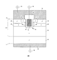
- FIG. It is a figure which shows the cross section of the unit structure in the vertical MOSFET100 of 1st Embodiment. It is a figure which shows the manufacturing flow 200 of the vertical MOSFET100 of 1st Embodiment. It is a figure which shows the outline
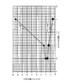
- FIG. It is a figure which shows the film-forming rate [nm / min] (vertical axis) of the silicon dioxide film with respect to the flow rate [sccm] (horizontal axis) of TEOS gas. It is a figure which shows the outline
- FIG. 4 is a diagram showing a carbon concentration [cm ⁇ 3 ] in a silicon dioxide film 36. 4 is a diagram showing a gallium concentration [cm ⁇ 3 ] in the silicon dioxide film 36. It is a figure which shows the cross section of the unit structure in the vertical MOSFET500 of 2nd Embodiment. It is a figure which shows the manufacturing flow 600 of the vertical MOSFET 500 of 2nd Embodiment.
- FIG. 1 is a diagram illustrating a cross section of a unit structure in the vertical MOSFET 100 according to the first embodiment.
- the semiconductor device of this example is a planar gate type vertical MOSFET 100 using gallium nitride.
- gallium nitride is abbreviated as GaN.
- the vertical MOSFET 100 of this example includes a GaN n + type substrate 10, an epitaxial layer 20 as a GaN semiconductor layer, a gate insulating film 32 and an interlayer insulating film 34, a gate electrode 42, a source electrode 52, and a drain electrode. 62.
- n or p means that electrons or holes are majority carriers, respectively.
- + means that the carrier concentration is higher than that in which it is not described, and ⁇ means that the carrier concentration is lower than that in which it is not described.
- E means a power of 10, for example, 1E + 16 means 1 ⁇ 10 16 .
- the n + type substrate 10 of this example is a GaN free-standing substrate.
- the GaN free-standing substrate may mean a substrate formed using only GaN, not a substrate having a GaN layer supported on a sapphire substrate or the like. However, the GaN free-standing substrate may have impurities of an element different from GaN.
- the n + type substrate 10 of this example includes one or more types of silicon (Si) and germanium (Ge) which are n-type impurities for GaN.
- p-type impurities for GaN are, for example, magnesium (Mg), calcium (Ca), beryllium (Be), and zinc (Zn).
- magnesium (Mg) is used as the p-type impurity.
- the epitaxial layer 20 is a GaN layer epitaxially formed on the n + type substrate 10.
- a direction from the n + type substrate 10 toward the epitaxial layer 20 is referred to as “up” or “upward”, and a direction opposite to the direction is referred to as “down” or “downward”.
- a portion positioned “upper” or “upper” may be referred to as “top”.
- a portion located “down” or “down” may be referred to as “bottom”.
- n - top type drift region 22, n - is the vicinity of the interface between the type drift region 22 and the gate insulating film 32 - n in the type drift region 22. Further, n - the bottom of the type drift region 22, n - is the vicinity of the interface between the type drift region 22 - n + -type substrate 10 and the n in the type drift region 22.
- the n + type substrate 10 and the epitaxial layer 20 are described as separate components.
- a configuration in which the n + type substrate 10 and the epitaxial layer 20 are combined may be referred to as a GaN substrate.
- the top of the GaN substrate corresponds to the vicinity of the front surface 21 of this example.
- the bottom of the GaN substrate corresponds to the vicinity of the back surface 11 of this example.
- the epitaxial layer 20 of this example has an n ⁇ type drift region 22, an n + type source region 24, a p + type contact region 26, and a p type well region 28 on the front surface 21 side.
- the n ⁇ type drift region 22 is an n ⁇ type region.
- At least a part of the p-type well region 28 may be exposed on the front surface 21 of the epitaxial layer 20.
- a gate insulating film 32 is provided on the p-type well region 28 exposed on the front surface 21.
- the vicinity of the p-type well region 28 exposed on the front surface 21 may function as a channel formation region 29.
- the p + type contact region 26 is provided at a position shallower than the p type well region 28.
- being shallower than the p-type well region 28 means that the bottom of the p + -type contact region 26 is located above the bottom of the p-type well region 28.
- the p + -type contact region 26 may have a function of reducing the contact resistance between the epitaxial layer 20 and the source electrode 52. In the vicinity of the interface between the p + -type contact region 26 and the source electrode 52, an alloy of GaN and the metal of the source electrode 52 may be formed.
- the n + type source region 24 is provided at a position shallower than the p + type contact region 26 and the p type well region 28.
- the shallower than the p + -type contact region 26 and the p-type well region 28 means that the bottom of the n + -type source region 24 is above the bottom of the p + -type contact region 26 and the p-type well region 28.
- the side of the n + type source region 24 is in contact with the p + type contact region 26 and the p type well region 28.
- the n + -type source region 24 may provide a path for electrons from the channel formation region 29 to the source electrode 52 during channel formation.
- the gate insulating film 32 in this example is a silicon dioxide film.
- the gate insulating film 32 of this example is provided so that the entire bottom is in direct contact with the front surface 21 of the epitaxial layer 20.
- the gate insulating film 32 in this example is provided between the gate electrode 42 and the p-type well region 28.
- the gate insulating film 32 in this example is a silicon dioxide film (SiO 2 ) formed by reacting TEOS gas and oxygen.
- the silicon dioxide film of this example has impurity atoms.
- the silicon dioxide film of this example includes carbon having a concentration of less than 2E + 18 [cm ⁇ 3 ].
- Carbon may function as a negative fixed charge in the silicon dioxide film by being combined with oxygen.
- the fixed charges in the gate insulating film 32 change the gate threshold voltage (V th ) from the design value. Therefore, it is desirable to suppress the fixed charges in the gate insulating film 32 as much as possible.
- the concentration of carbon in the silicon dioxide film is less than 2E + 18 [cm ⁇ 3 ], more preferably 1E + 18 [cm ⁇ 3 ] or less. Thereby, the deviation from the design value of the gate threshold voltage (V th ) can be suppressed. Moreover, it is possible to prevent the gate threshold voltage (V th ) from varying for each different channel formation region 29.
- the gate electrode 42 is provided in direct contact with the gate insulating film 32.
- the gate electrode 42 of this example extends in the back or front direction of the paper and is electrically connected to the gate terminal 40.
- the gate terminal 40 may receive an on signal for generating a channel in the channel formation region 29 or an off signal gate signal for eliminating the channel.
- the interlayer insulating film 34 is provided on the gate electrode 42 and the epitaxial layer 20.
- the interlayer insulating film 34 may electrically insulate the gate electrode 42 and the source electrode 52 from each other.
- the interlayer insulating film 34 of this example covers the top of the gate electrode 42 and the sides of the gate electrode 42 and the gate insulating film 32.
- the bottom of the interlayer insulating film 34 in this example is in direct contact with the front surface 21 of the epitaxial layer 20.
- the interlayer insulating film 34 may be any one of a silicon oxide film, a silicon nitride film, and a resin film.
- the interlayer insulating film 34 in this example is a silicon dioxide film formed by the same method as the gate insulating film 32.
- the source electrode 52 is provided on the front surface 21 and the interlayer insulating film 34.
- the bottom of the source electrode 52 in this example is in direct contact with the n + type source region 24 and the p + type contact region 26.
- the source electrode 52 in this example is electrically connected to the source terminal 50.
- the source terminal 50 may have a ground potential.
- the drain electrode 62 is provided in direct contact with the bottom surface 11 of the n + type substrate 10.
- the drain electrode 62 in this example is electrically connected to the drain terminal 60.
- a voltage corresponding to the energization current of the vertical MOSFET 100 may be applied to the drain terminal 60.
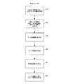
- FIG. 2 is a diagram showing a manufacturing flow 200 of the vertical MOSFET 100 of the first embodiment. In the manufacturing method of this example, steps S10 to S60 are performed in this order.
- Step S ⁇ b> 10 is a step of forming the epitaxial layer 20 on the n + type substrate 10.
- the n + type substrate 10 may have an n type impurity concentration of 1E + 19 [cm ⁇ 3 ] or more and 1E + 20 [cm ⁇ 3 ] or less.
- the n-type impurity concentration of the epitaxial layer 20 may be about 1E + 16 [cm ⁇ 3 ].
- the epitaxial layer 20 may be formed by MOCVD (Metal Organic Chemical Vapor Deposition).
- MOCVD Metal Organic Chemical Vapor Deposition
- the epitaxial layer 20 is formed by MOCVD using trimethyl gallium (TMG), ammonia (NH 3 ), and a suitable carrier gas.
- TMG trimethyl gallium
- NH 3 ammonia
- the thickness of the n + type substrate 10 may be 100 [ ⁇ m] to 300 [ ⁇ m]
- the thickness of the epitaxial layer 20 may be 10 [ ⁇ m].
- Step S20 is a step of forming the n + type source region 24, the p + type contact region 26, and the p type well region 28.
- the epitaxial layer 20 is doped with p-type and n-type impurities, and then the epitaxial layer 20 is annealed. Thereby, the n + type source region 24, the p + type contact region 26, and the p type well region 28 are formed.
- Mg ions accelerated at 180 [keV] are implanted at a concentration of 2E + 14 [cm ⁇ 2 ].
- Mg ions accelerated at 45 [keV] are implanted at a concentration of 2E + 15 [cm ⁇ 2 ].
- Si ions accelerated at 45 [keV] are implanted at a concentration of 5E + 15 [cm ⁇ 2 ].
- a photoresist mask having a predetermined opening pattern may be used for ion implantation.
- a cap layer is provided on the front surface 21 after ion implantation.
- the cap layer may be silicon dioxide.
- the epitaxial layer 20 is annealed. Accordingly, the n + type source region 24 having an n type impurity concentration of 1E + 20 [cm ⁇ 3 ], the p + type contact region 26 having a p type impurity concentration of 4E + 19 [cm ⁇ 3 ], and a p type impurity concentration of 1E + 17 [ cm ⁇ 3 ] p-type well region 28 may be formed. Note that the cap layer may be removed after annealing.
- Step S30 is a step of forming the gate insulating film 32.
- the gate insulating film 32 in this example is a silicon dioxide film.
- the silicon dioxide film is patterned into the shape of the gate insulating film 32 after being formed.
- the step of forming the silicon dioxide film includes a step of supplying TEOS gas as a silicon raw material.
- the epitaxial layer 20 in this example is made of a GaN material. Therefore, the gate insulating film 32 (silicon dioxide film) cannot be formed on the epitaxial layer 20 by thermally oxidizing the epitaxial layer 20.
- the step of forming the silicon dioxide film further includes the step of supplying oxygen gas as an oxygen source and forming the silicon dioxide film by plasma CVD (Chemical Vapor Deposition). That is, in this example, a silicon dioxide film is formed by plasma CVD using TEOS gas as a silicon source and oxygen (O 2 ) gas as an oxygen source.
- plasma CVD Chemical Vapor Deposition
- the gallium of the epitaxial layer 20 is taken into the silicon dioxide film.
- gallium functions as a positive charge.
- the concentration of gallium in the silicon dioxide film can be reduced by devising the film formation rate as described later. Thereby, the deviation from the design value of the gate threshold voltage (V th ) can be suppressed.
- the formation of the silicon dioxide film of this example will be described in detail with reference to FIGS.
- Step S40 is a step of forming the gate electrode.
- the gate electrode 42 may be polysilicon. Polysilicon may be deposited on the gate insulating film 32 and then patterned into the shape of the gate electrode 42.
- Step S50 is a step in which the interlayer insulating film 34 is formed.
- the interlayer insulating film 34 in this example is a silicon dioxide film formed by the same plasma CVD as the gate insulating film 32. After the interlayer insulating film 34 is formed on the gate electrode 42, the interlayer insulating film 34 may be patterned so as to remain on the top of the gate electrode 42 and the sides of the gate electrode 42 and the gate insulating film 32.
- Step S60 is a step of forming the source electrode 52 and the drain electrode 62.
- the source electrode 52 and the drain electrode 62 in this example may be a laminate of a Ti (titanium) layer and an Al (aluminum) layer.
- a Ti layer may be provided in direct contact with the front surface 21, and an Al layer may be provided on the Ti layer.
- the drain electrode 62 a Ti layer may be provided in direct contact with the back surface 11, and an Al layer may be provided under the Ti layer. Thereby, the vertical MOSFET 100 is completed.
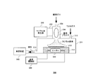
- FIG. 3 is a diagram showing an outline of a manufacturing apparatus 300 for forming a silicon dioxide film.
- the manufacturing apparatus 300 of this example includes a reaction chamber 311, a temperature adjustment unit 330, a vacuum device 340, a microwave generator 350, a waveguide 352, and a plasma generation chamber 354.
- the reaction chamber 311 has a pedestal 312 made of Al.
- the work 310 may be fixed on the pedestal 312 using electrostatic attraction.
- Work 310 includes n + type substrate 10 and epitaxial layer 20.
- a heater 320 is provided inside the pedestal 312.
- the temperature adjusting unit 330 can control the temperature of the heater 320 in a range of 100 [° C.] to 450 [° C.]. Since the pedestal 312 has very good thermal conductivity, the temperature of the heater 320 can be regarded as the temperature of the workpiece 310.
- the temperature adjusting unit 330 in this example heats the workpiece 310 at a temperature of 300 [° C.] or more and 400 [° C.] or less in the step of forming the silicon dioxide film as the gate insulating film 32 and the interlayer insulating film 34.
- the vacuum device 340 sucks the gas in the reaction chamber 311 from the exhaust port 314.
- the vacuum apparatus 340 may control the atmospheric pressure in the reaction chamber 311 from 200 [Pa] to 300 [Pa].
- the microwave generator 350 is connected to the plasma generation chamber 354 through the waveguide 352.
- the microwave generator 350 converts oxygen (O 2 ) introduced into the plasma generation chamber 354 from the inlet 356 into plasma.
- Plasmaized oxygen travels into the reaction chamber 311.
- Plasmaized oxygen is shown as radical oxygen in the reaction chamber 311.
- TEOS gas is introduced from the inlet 316 into the reaction chamber 311.
- TEOS reacts with radical oxygen.
- a silicon dioxide film is deposited on the front surface 21 of the epitaxial layer 20.
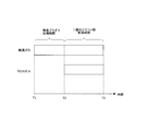
- FIG. 4 is a diagram for explaining an oxygen plasma treatment period and a silicon dioxide film formation period in the manufacturing apparatus 300.
- the horizontal axis indicates time, and the vertical axis indicates the type of gas.
- oxygen gas is continuously supplied to the reaction chamber 311 at a flow rate of 90 [sccm] from time T1 to time T3.
- the period from time T1 to time T2 is an oxygen plasma treatment period.
- TEOS gas is supplied to the reaction chamber 311 at a flow rate of 0.25 [sccm] to 2 [sccm].
- the period from time T2 to time T3 is the silicon dioxide film formation period.
- FIG. 5 is a diagram showing the deposition rate [nm / min] (vertical axis) of the silicon dioxide film with respect to the flow rate [sccm] (horizontal axis) of the TEOS gas.
- the upper graph shown by the square plot is the result when the workpiece 310 is heated at 300 [° C.].
- the lower graph shown by the rhombus plot is a result when the workpiece 310 is heated at 400 [° C.].
- a silicon dioxide film as an interlayer insulating film may be formed using TEOS gas in plasma CVD.
- the silicon dioxide film can be formed at a lower temperature than the thermal oxide film. Further, the silicon dioxide film can be formed with low damage to the formation film formation surface and the structure located below the formation film formation surface.
- a silicon dioxide film formed using TEOS gas in plasma CVD has a problem of capturing fixed charges such as carbon. Therefore, a silicon dioxide film formed using TEOS gas in plasma CVD is used as an interlayer insulating film, but not used as a gate insulating film.
- the higher the film formation rate of silicon dioxide the easier the carbon in the TEOS gas is taken into the silicon dioxide film. Therefore, in this example, the flow rate of the TEOS gas and the temperature of the work 310 are controlled in consideration of the film formation rate. This controlled the carbon concentration in silicon dioxide.
- gallium contamination in the silicon dioxide film is an inherent problem when the silicon dioxide film is formed on the GaN layer. That is, gallium is not mixed into the silicon dioxide film in the MOSFET of the Si substrate and the MOSFET of the SiC substrate.
- the silicon dioxide film is formed on the epitaxial layer 20 at a deposition rate of 5 [nm / min] or less.
- the film formation rate may be 5 [nm / min], 2.5 [nm / min], or 1 [nm / min].
- the inventor of the present application reduces the fixed charge to an allowable amount when the flow rate of the TEOS gas is 0.5 [sccm] or less. I found out.
- the flat band voltage Vfb which is an index for evaluating the charge amount in the film, could be 1 [V] or less.
- the flow rate of TEOS gas is 0.25 [sccm] or more and 1 [ sccm] or less.
- the flow rate of the TEOS gas may be 0.25 [sccm] or more and 0.5 [sccm] or less.
- the maximum value of the flow rate of the TEOS gas may be 0.5 [sccm] or more and 1 [sccm] or less when the temperature of the work 310 is 300 [° C.] or more and 400 [° C.] or less. It can be said that the minimum value of the gas flow rate may be 0.25 [sccm].
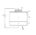
- FIG. 6A is a diagram illustrating an outline of the element 400 in which a flat band voltage is measured.
- an n ⁇ -type GaN epitaxial layer 20 was provided on a GaN n + -type substrate 10.
- the epitaxial layer 20 is not provided with the n + type source region 24, the p + type contact region 26, and the p type well region 28.
- a silicon dioxide film 36 was formed on the epitaxial layer 20 by the above-described method. Note that the temperature of the workpiece 310 during the formation of the silicon dioxide film 36 was set to 300 [° C.].
- an Al metal layer 44 was provided on the silicon dioxide film 36.
- a variable voltage was applied between the metal layer 44 and the n + type substrate 10 to evaluate the capacitance-voltage (CV) characteristics of the element 400 as a MOS capacitor.
- the element 400 three types of elements 400 with a TEOS gas flow rate of 2 [sccm], 1 [sccm], and 0.5 [sccm] were prepared. First, the CV characteristics of the three types of elements 400 were evaluated. Next, the three types of elements 400 were annealed at 400 [° C.]. Note that 10 [vol%] hydrogen (H 2 ) and 90 [vol%] nitrogen (N 2 ) were used as the atmosphere gas during annealing. The atmospheric pressure was 1 atm. Then, the CV characteristics of the three types of elements 400 after annealing were evaluated.
- carbon in the silicon dioxide film 36 is considered to function as a negative charge.
- carbon and hydrogen are combined in the silicon dioxide film 36, carbon is considered to function as a positive charge.
- gallium in the silicon dioxide film 36 functions as a negative charge.
- FIG. 6B is a diagram showing a flat band voltage V fb [V] (vertical axis) with respect to the flow rate [sccm] (horizontal axis) of the TEOS gas.
- V fb flat band voltage
- the flow rate of TEOS gas was 2 [sccm], 1 [sccm], and 0.5 [sccm]
- V fb before and after annealing was measured, respectively.
- the upper graph shown by the diamond plot is V fb before annealing.
- the lower graph shown by the square plot is V fb after annealing.
- V fb When V fb is positive, it means that the negative charge is larger than the positive charge in the silicon dioxide film 36. That is, when V fb is positive, the main fixed charge in the silicon dioxide film 36 is a negative charge. Further, when V fb is negative, it means that the positive charge in the silicon dioxide film 36 is larger than the negative charge. That is, when V fb is negative, the main fixed charge in the silicon dioxide film 36 is a positive charge.
- V fb The smaller the absolute value of V fb, the smaller the fixed charge in the silicon dioxide film 36.
- V fb was the smallest as compared with other flow rate examples. Specifically, V fb was 1 [V] under the condition of 0.5 [sccm] before annealing. Further, V fb became ⁇ 1.2 [V] under the condition of 0.5 [sccm] after annealing.
- the absolute value of V fb of the silicon dioxide film 36 as the gate insulating film 32 in the vertical MOSFET 100 may be regarded as 1 [V].
- the absolute value of V fb also decreases as the TEOS gas flow rate decreases from 2 [sccm] to 0.5 [sccm], so the TEOS gas flow rate is 0.5 [ It can be said that the absolute value of V fb is 1 [V] or less at [sccm] or less. Therefore, it can be said that the absolute value of V fb is also 1 [V] or less in the silicon dioxide film 36 formed with the TEOS gas flow rate of 0.25 [sccm].
- FIG. 7 is a diagram showing the carbon concentration [cm ⁇ 3 ] in the silicon dioxide film 36.
- the horizontal axis indicates the depth [nm] from the upper surface of the silicon dioxide film 36.
- the vertical axis represents the carbon concentration [cm ⁇ 3 ].
- the carbon concentration was evaluated by SIMS (Secondary Ion Mass Spectrometry).
- the temperature of the workpiece 310 when the silicon dioxide film 36 was formed was 300 [° C.].
- three types of elements 400 were prepared in which the flow rate of the TEOS gas was 2 [sccm], 0.5 [sccm], and 0.25 [sccm]. Data of 2 [sccm] and 0.5 [sccm] are indicated by thin lines, and data of 0.25 [sccm] are indicated by thick lines.
- the position of the interface between the silicon dioxide film 36 and the epitaxial layer 20 varies depending on the flow rate of the TEOS gas.
- the position of the interface at 2 [sccm] is a position having a depth of 144 [nm].
- the position of the interface at 0.5 [sccm] is a position at a depth of 111 [nm].
- the position of the interface at 0.25 [sccm] is a position at a depth of 94 [nm].
- the detection limit of carbon was 5E + 17 [cm ⁇ 3 ].
- the impurity concentration below the detection limit is also detected, but the impurity concentration below the detection limit is not reliable and accurate.
- the region of 0 [nm] to 30 [nm] on the horizontal axis normal data could not be obtained due to the influence of surface contamination. Therefore, the numerical value of the area is not taken into consideration.
- the carbon in the silicon dioxide film 36 was less than 2E + 18 [cm ⁇ 3 ].
- the carbon concentration may be evaluated by a numerical value excluding the influence of noise and abnormal values.
- the arithmetic average or logarithmic average of the carbon concentration from the interface to a position on a predetermined length in the silicon dioxide film 36 may be the carbon concentration of the silicon dioxide film 36.
- the carbon concentration in the case of 0.25 [sccm] is 1E + 18 [cm ⁇ 3 ] or less.
- the flow rate of TEOS gas is 0.5 [sccm]
- the carbon concentration in the silicon dioxide film 36 is 1E + 18 [cm ⁇ 3 ] or less considering that noise and abnormal values are acquired. can do.
- the carbon concentration of the silicon dioxide film 36 formed using TEOS gas is equal to or higher than a predetermined concentration.
- the carbon concentration of the silicon dioxide film 36 formed using TEOS gas is larger than 0 [cm ⁇ 3 ]. Therefore, the silicon dioxide film 36 of this example is silicon dioxide at any position above the interface that is less than 64 nm from the interface with the epitaxial layer 20 (or less than half the thickness of the silicon dioxide film 36).
- carbon concentration of the membrane 36, 0 may be large 2E + 18 less than [cm -3] from [cm -3], 1E + 17 [cm -3] or more 2E + 18 may be less than [cm -3], 3E + 17 [cm - 3 ] or more and less than 2E + 18 [cm ⁇ 3 ], or 5E + 17 [cm ⁇ 3 ] or more and less than 2E + 18 [cm ⁇ 3 ].
- FIG. 8 is a diagram showing the gallium concentration [cm ⁇ 3 ] in the silicon dioxide film 36.
- the horizontal axis indicates the depth [nm] from the upper surface of the silicon dioxide film 36.
- the vertical axis represents the gallium concentration [cm ⁇ 3 ].
- the gallium concentration is measured by SIMS (Secondary Ion Mass. Evaluation was carried out by Spectrometry).
- the temperature of the workpiece 310 when the silicon dioxide film 36 was formed was 300 [° C.].
- three types of elements 400 were prepared in which the flow rate of the TEOS gas was 2 [sccm], 0.5 [sccm], and 0.25 [sccm]. Data of 2 [sccm] and 0.5 [sccm] are indicated by thin lines, and data of 0.25 [sccm] are indicated by thick lines.
- the detection limit of gallium was 8E + 15 [cm ⁇ 3 ].
- the interface between the silicon dioxide film 36 and the epitaxial layer 20 is matched in each data of 2 [sccm], 0.5 [sccm], and 0.25 [sccm].
- the gallium concentration attenuates from the peak and gradually approaches a constant value.
- the intersection with the graph when the constant value of the gallium concentration is extrapolated to the left in the horizontal axis is the interface between the silicon dioxide film 36 and the epitaxial layer 20.
- the interface corresponds to a position of 128 [nm] on the horizontal axis. In the region of 0 [nm] to 60 [nm] on the horizontal axis, normal data could not be obtained due to the influence of surface contamination. Therefore, the numerical value of the area is not taken into consideration.
- gallium is more easily taken into the silicon dioxide film 36 as the flow rate of the TEOS gas increases.
- the gallium concentration in the silicon dioxide film 36 is 1E + 17 [cm ⁇ 3 ] at a position 10 [nm] or more above the front surface 21 of the GaN epitaxial layer 20. It became the following. Since the gallium concentration is too high in the vicinity of the interface between the silicon dioxide film 36 and the GaN epitaxial layer 20, a position at a depth of 118 [nm] away from the interface by 10 [nm] was selected in this experimental example.
- the gallium concentration in the range from the position of depth 118 [nm] to the position of depth 60 [nm] was 1E + 17 [cm ⁇ 3 ] or less. According to the result of this experiment, it can be said that the gallium concentration in this range is 3E + 16 [cm ⁇ 3 ] or less in the case of 0.25 [sccm]. Further, in consideration of noise and abnormal values, it can be said that the gallium concentration in the range is 2E + 16 [cm ⁇ 3 ] or less in the case of 0.25 [sccm].
- the gallium concentration of the silicon dioxide film 36 is 1E + 17 [cm ⁇ 3 ] or less at all positions above the interface that is 10 nm or more and less than 68 nm from the interface with the epitaxial layer 20.
- the thickness of the silicon dioxide film 36 of this example is 128 nm, the half thickness is 64 nm. Therefore, the gallium concentration of the silicon dioxide film 36 is 1E + 17 [cm ⁇ 3 ] or less at an arbitrary position above 10 nm or more and less than half the thickness of the silicon dioxide film 36 from the interface with the epitaxial layer 20.
- the above-mentioned carbon concentration range is also satisfied from the interface with the epitaxial layer 20 to the position of half the thickness of the silicon dioxide film 36 (that is, 64 nm above the interface). Therefore, the concentration of impurity atoms contained in the silicon dioxide film 36 is in the above range at any position above the interface with the epitaxial layer 20 that is 10 nm or more and less than half the thickness of the silicon dioxide film 36. The concentration and the gallium concentration may be met.
- FIG. 9 is a diagram showing a cross section of a unit structure in the vertical MOSFET 500 of the second embodiment.
- the semiconductor device of this example is a trench gate type vertical MOSFET 500 using GaN.
- a trench portion 70 is provided in the epitaxial layer 20.
- the gate insulating film 32 which is a silicon dioxide film, is provided in direct contact with the bottom and sides of the trench portion 70.
- the gate electrode 42 is provided in the trench portion 70 in contact with the gate insulating film 32.
- the gate insulating film 32 on the side of the trench portion 70 is located between the side of the gate electrode 42 and the n + -type source region 24 and the p-type well region 28.
- the channel formation region 29 is located in the p-type well region 28 on the side portion of the trench portion 70.
- the interlayer insulating film 34 is provided on the trench portion 70.
- the interlayer insulating film 34 in this example is in direct contact with the upper portions of the gate insulating film 32 and the gate electrode 42 and the upper portion of the n + type source region 24. This is different from the first embodiment. Other points may be the same as in the first embodiment.
- the silicon dioxide film as the gate insulating film 32 and the interlayer insulating film 34 may be the silicon dioxide film of the first embodiment.
- FIG. 10 is a diagram showing a manufacturing flow 600 of the vertical MOSFET 500 of the second embodiment.
- This example has step S12 which forms trench part 70 between step S10 and step S30.
- the step S42 for forming the n + -type source region 24, the p + -type contact region 26 and the p-type well region 28 (corresponding to step S20 in the manufacturing flow 200) is a step for forming the gate electrode 42. It is located between S40 and step S50 of forming the interlayer insulating film 34. This is different from the first embodiment. Other points may be the same as in the first embodiment. Also in this example, the same effect as that of the first embodiment can be obtained.
- Pedestal 314 ... Exhaust port, 316 ... Inlet port, 320 ... Heater, 330 ... Temperature control unit, 340 ... ⁇ true Empty device, 350 ... Microwave generator, 352 ... Waveguide, 354 ... Plasma generation chamber, 356 ... Inlet, 400 ... Element, 500 ... Vertical MOSFET, 600 ... Manufacturing flow
Landscapes
- Chemical & Material Sciences (AREA)
- Engineering & Computer Science (AREA)
- Mechanical Engineering (AREA)
- Chemical Kinetics & Catalysis (AREA)
- General Chemical & Material Sciences (AREA)
- Materials Engineering (AREA)
- Inorganic Chemistry (AREA)
- Metallurgy (AREA)
- Organic Chemistry (AREA)
- Insulated Gate Type Field-Effect Transistor (AREA)
- Physics & Mathematics (AREA)
- Plasma & Fusion (AREA)
- Formation Of Insulating Films (AREA)
Abstract
TEOS(オルトケイ酸テトラエチル:Si(OC2H5)4)を用いて半導体基板上にSiO2膜を形成する場合、当該SiO2膜に炭素(C)が混入する場合がある。SiO2膜に炭素は固定電荷として機能し得る。例えば、MOSFET(Metal-Oxide-Semiconductor Field-Effect Transistor)のゲート絶縁膜としてのSiO2膜に炭素(C)が混入した場合、ゲート閾値電圧(Vth)が変動する問題がある。窒化ガリウム半導体層を用いた半導体装置であって、少なくとも一部が窒化ガリウム半導体層に直接接して設けられ、不純物原子を有する二酸化シリコン膜を備え、二酸化シリコン膜は、不純物原子として、0cm-3より大きく2E+18cm-3未満の濃度の炭素と、1E+17cm-3以下の濃度のガリウムを含む半導体装置を提供する。
Description
本発明は、半導体装置および半導体装置の製造方法に関する。
従来、熱酸化法により二酸化シリコンのゲート絶縁膜を形成していた(例えば、特許文献1参照)。
[先行技術文献]
[特許文献]
[特許文献1] 特開2015-162578号公報
[先行技術文献]
[特許文献]
[特許文献1] 特開2015-162578号公報
TEOS(オルトケイ酸テトラエチル:Si(OC2H5)4)を用いて半導体基板上に二酸化シリコン(SiO2)膜を形成する場合、当該二酸化シリコン膜に炭素(C)が混入する場合がある。二酸化シリコン膜において、炭素は固定電荷として機能し得る。例えば、MOSFET(Metal-Oxide-Semiconductor Field-Effect Transistor)のゲート絶縁膜として二酸化シリコン膜を用いる場合、二酸化シリコン膜中の炭素に起因してゲート閾値電圧(Vth)が変動する問題がある。
本発明の第1の態様においては、窒化ガリウム半導体層を用いた半導体装置を提供する。窒化ガリウム半導体層は、二酸化シリコン膜を備えてよい。二酸化シリコン膜は、少なくとも一部が窒化ガリウム半導体層に直接接して設けられてよい。二酸化シリコン膜は、不純物原子を有してよい。二酸化シリコン膜は、不純物原子として、0cm-3より大きく2E+18cm-3未満の濃度の炭素を含んでよい。二酸化シリコン膜は、不純物原子として、1E+17cm-3以下の濃度のガリウムを含んでよい。
不純物原子の濃度は、窒化ガリウム半導体層のおもて面から10nm以上、二酸化シリコン膜の半分の厚さ未満である上方の任意の位置における濃度であってよい。
半導体装置は、ゲート電極をさらに備えてよい。ゲート電極は、二酸化シリコン膜上に直接接して設けられてよい。窒化ガリウム半導体層は、二酸化シリコン膜が設けられたおもて面側にp型ウェル領域を有してよい。p型ウェル領域は、窒化ガリウム半導体層に対するp型不純物を有してよい。二酸化シリコン膜は、ゲート絶縁膜であってよい。ゲート絶縁膜は、ゲート電極とp型ウェル領域との間に設けられてよい。
二酸化シリコン膜は、層間絶縁膜であってよい。層間絶縁膜は、窒化ガリウム半導体層上に設けられてよい。
本発明の第2の態様においては、窒化ガリウム半導体層を有する半導体装置の製造方法を提供する。半導体装置の製造方法は、二酸化シリコン膜を形成する段階を備えてよい。二酸化シリコン膜は、不純物原子を有してよい。シリコン酸化の少なくとも一部は、窒化ガリウム半導体層に直接接するように形成されてよい。二酸化シリコン膜は、不純物原子として、2E+18cm-3未満の濃度の炭素を含んでよい。二酸化シリコン膜は、不純物原子として、5E+17cm-3以上の濃度の炭素を含んでもよい。二酸化シリコン膜は、不純物原子として、1E+17cm-3以下の濃度のガリウムを含んでよい。
二酸化シリコン膜を形成する段階は、シリコンの原料としてTEOSガスを供給する段階を含んでよい。
二酸化シリコン膜を形成する段階は、酸素の原料として酸素ガスを供給し、プラズマCVDにより二酸化シリコン膜を形成する段階を含んでよい。
二酸化シリコン膜を形成する段階において、窒化ガリウム半導体層上に二酸化シリコン膜を5nm/min以下の成膜レートで形成してよい。
二酸化シリコン膜を形成する段階において、窒化ガリウム半導体層を300℃以上400℃以下の温度で加熱してよい。
なお、上記の発明の概要は、本発明の必要な特徴の全てを列挙したものではない。また、これらの特徴群のサブコンビネーションもまた、発明となりうる。
以下、発明の実施の形態を通じて本発明を説明するが、以下の実施形態は請求の範囲にかかる発明を限定するものではない。また、実施形態の中で説明されている特徴の組み合わせの全てが発明の解決手段に必須であるとは限らない。
図1は、第1実施形態の縦型MOSFET100における単位構造断面を示す図である。本例の半導体装置は、窒化ガリウムを用いたプレーナーゲート型の縦型MOSFET100である。なお、以下において、窒化ガリウムをGaNと略記する。本例の縦型MOSFET100は、GaNのn+型基板10と、GaN半導体層としてのエピタキシャル層20と、ゲート絶縁膜32および層間絶縁膜34と、ゲート電極42と、ソース電極52と、ドレイン電極62とを備える。
本例において、nまたはpは、それぞれ電子または正孔が多数キャリアであることを意味する。また、nまたはpの右肩に記載した+または-について、+はそれが記載されていないものよりもキャリア濃度が高く、-はそれが記載されていないものよりもキャリア濃度が低いことを意味する。また、本例において、Eは10のべき乗を意味し、例えば1E+16は、1×10¹⁶を意味する。
本例のn+型基板10は、GaNの自立基板である。GaNの自立基板とは、サファイア基板等の上に支持されたGaN層を有する基板ではなく、GaNのみを用いて形成した基板を意味してよい。ただし、GaNの自立基板は、GaNとは異なる元素の不純物を有してもよい。
本例のn+型基板10は、GaNに対するn型不純物であるシリコン(Si)およびゲルマニウム(Ge)の一種類以上を含む。なお、GaNに対するp型不純物は、例えば、マグネシウム(Mg)、カルシウム(Ca)、ベリリウム(Be)および亜鉛(Zn)である。本例においては、p型不純物としてマグネシウム(Mg)を用いる。
エピタキシャル層20は、n+型基板10上にエピタキシャル形成されたGaN層である。本例においては、n+型基板10からエピタキシャル層20に向かう方向を「上」または「上方」と称し、当該方向とは反対の方向を「下」または「下方」と称する。また、本例では、領域または構成物において、「上」または「上方」に位置する部分を「頂部」と称する場合がある。また、領域または構成物において、「下」または「下方」に位置する部分を「底部」と称する場合がある。例えば、n-型ドリフト領域22の頂部は、n-型ドリフト領域22におけるn-型ドリフト領域22とゲート絶縁膜32との界面近傍である。また、n-型ドリフト領域22の底部は、n-型ドリフト領域22におけるn+型基板10とn-型ドリフト領域22との界面近傍である。
なお、本例においては、説明の便宜上、n+型基板10とエピタキシャル層20とを別個の構成物として記載する。しかしながら、他の例においては、n+型基板10とエピタキシャル層20とを合わせた構成を、GaN基板と称してもよい。当該他の例において、GaN基板の頂部は、本例のおもて面21近傍に対応する。また、GaN基板の底部は、本例のうら面11近傍に対応する。
本例のエピタキシャル層20は、おもて面21側にn-型ドリフト領域22と、n+型ソース領域24と、p+型コンタクト領域26と、p型ウェル領域28とを有する。n-型ドリフト領域22は、n-型の領域である。p型ウェル領域28は、少なくとも一部がエピタキシャル層20のおもて面21に露出してよい。本例において、おもて面21に露出したp型ウェル領域28上には、ゲート絶縁膜32が設けられる。おもて面21に露出したp型ウェル領域28の近傍は、チャネル形成領域29として機能してよい。
p+型コンタクト領域26は、p型ウェル領域28よりも浅い位置に設けられる。本例において、p型ウェル領域28よりも浅いとは、p+型コンタクト領域26の底部がp型ウェル領域28の底部よりも上方に位置することを意味する。p+型コンタクト領域26は、エピタキシャル層20とソース電極52とのコンタクト抵抗を下げる機能を有してよい。p+型コンタクト領域26とソース電極52との界面付近においては、GaNとソース電極52の金属との合金が形成されてよい。
n+型ソース領域24は、p+型コンタクト領域26およびp型ウェル領域28よりも浅い位置に設けられる。本例において、p+型コンタクト領域26およびp型ウェル領域28よりも浅いとは、n+型ソース領域24の底部が、p+型コンタクト領域26およびp型ウェル領域28の底部よりも上方に位置することを意味する。また、本例において、n+型ソース領域24の側部は、p+型コンタクト領域26およびp型ウェル領域28に接する。n+型ソース領域24は、チャネル形成時に電子がチャネル形成領域29からソース電極52に至る経路を提供してよい。
本例のゲート絶縁膜32は、二酸化シリコン膜である。本例のゲート絶縁膜32は、底部全体がエピタキシャル層20のおもて面21に直接接して設けられる。本例のゲート絶縁膜32は、ゲート電極42とp型ウェル領域28との間に設けられる。本例のゲート絶縁膜32は、TEOSガスと酸素とを反応させて形成した二酸化シリコン膜(SiO2)である。本例の二酸化シリコン膜は、不純物原子を有する。具体的には、本例の二酸化シリコン膜は、2E+18[cm-3]未満の濃度の炭素を含む。
炭素は、酸素と結びつくことにより、二酸化シリコン膜中において負の固定電荷として機能する場合がある。ゲート絶縁膜32中の固定電荷はゲート閾値電圧(Vth)を設計値から変動させる。それゆえ、ゲート絶縁膜32中の固定電荷はできるだけ抑制することが望ましい。本例では、二酸化シリコン膜中の炭素の濃度を2E+18[cm-3]未満、さらに望ましくは、1E+18[cm-3]以下とする。これにより、ゲート閾値電圧(Vth)の設計値からのずれを抑制することができる。また、異なるチャネル形成領域29毎にゲート閾値電圧(Vth)がばらつくことを防ぐことができる。
ゲート電極42は、ゲート絶縁膜32上に直接接して設けられる。本例のゲート電極42は、紙面奥または手前方向に延伸して、ゲート端子40に電気的に接続する。ゲート端子40には、チャネル形成領域29においてチャネルを生成するオン信号またはチャネルを消滅させるオフ信号のゲート信号が入力されてよい。
層間絶縁膜34は、ゲート電極42およびエピタキシャル層20上に設けられる。層間絶縁膜34は、ゲート電極42とソース電極52とを電気的に絶縁してよい。本例の層間絶縁膜34は、ゲート電極42の頂部と、ゲート電極42およびゲート絶縁膜32の側部とを覆う。本例の層間絶縁膜34の底部は、エピタキシャル層20のおもて面21に直接接する。
層間絶縁膜34は、酸化シリコン膜、窒化シリコン膜および樹脂膜のいずれかであってよい。本例の層間絶縁膜34は、ゲート絶縁膜32と同じ手法で形成された二酸化シリコン膜である。
ソース電極52は、おもて面21および層間絶縁膜34上に設けられる。本例のソース電極52の底部は、n+型ソース領域24およびp+型コンタクト領域26に直接接する。本例のソース電極52は、ソース端子50に電気的に接続する。ソース端子50は、接地電位を有してよい。ドレイン電極62は、n+型基板10のうら面11下に直接接して設けられる。本例のドレイン電極62は、ドレイン端子60に電気的に接続する。ドレイン端子60には、縦型MOSFET100の通電電流に応じた電圧が印加されてよい。
図2は、第1実施形態の縦型MOSFET100の製造フロー200を示す図である。本例の製造方法において、段階S10から段階S60はこの順に行われる。
段階S10は、n+型基板10上にエピタキシャル層20を形成する段階である。n+型基板10のn型不純物濃度は、1E+19[cm-3]以上1E+20[cm-3]以下であってよい。エピタキシャル層20のn型不純物濃度は、1E+16[cm-3]程度であってよい。エピタキシャル層20は、MOCVD(Metal Organic Chemical Vapor Deposition)により形成されてよい。例えば、エピタキシャル層20は、トリメチルガリウム(TMG)、アンモニア(NH3)および適切なキャリアガスを用いて、MOCVDにより形成される。縦型MOSFET100が1200Vの耐圧を有する場合、n+型基板10の厚みは100[μm]~300[μm]とし、エピタキシャル層20の厚みは10[μm]としてよい。
段階S20は、n+型ソース領域24、p+型コンタクト領域26およびp型ウェル領域28を形成する段階である。段階S20では、エピタキシャル層20にp型およびn型不純物をドーピングし、その後、エピタキシャル層20をアニールする。これにより、n+型ソース領域24、p+型コンタクト領域26およびp型ウェル領域28を形成する。
本例では、p型ウェル領域28を形成するべく、180[keV]で加速したMgイオンを2E+14[cm-2]の濃度で注入する。また、p+型コンタクト領域26を形成するべく、45[keV]で加速したMgイオンを2E+15[cm-2]の濃度で注入する。さらに、n+型ソース領域24を形成するべく、45[keV]で加速したSiイオンを5E+15[cm-2]の濃度で注入する。なお、イオン注入に際しては、所定の開口パターンを有するフォトレジストマスクを用いてよい。
イオン注入後に、おもて面21にキャップ層を設ける。キャップ層は、二酸化シリコンであってよい。その後、エピタキシャル層20をアニールする。これにより、n型不純物濃度が1E+20[cm-3]のn+型ソース領域24、p型不純物濃度が4E+19[cm-3]のp+型コンタクト領域26、および、p型不純物濃度が1E+17[cm-3]のp型ウェル領域28を形成してよい。なお、アニール後においてキャップ層は除去してよい。
段階S30は、ゲート絶縁膜32を形成する段階である。上述の様に、本例のゲート絶縁膜32は、二酸化シリコン膜である。二酸化シリコン膜は、成膜後において、ゲート絶縁膜32の形状にパターニングする。
本例において、二酸化シリコン膜を形成する段階は、シリコンの原料としてTEOSガスを供給する段階を含む。本例のエピタキシャル層20は、GaN材料からなる。それゆえ、エピタキシャル層20を熱酸化することによりエピタキシャル層20上にゲート絶縁膜32(二酸化シリコン膜)を形成することはできない。
本例において、二酸化シリコン膜を形成する段階は、酸素の原料として酸素ガスを供給し、プラズマCVD(Chemical Vapor Deposition)により二酸化シリコン膜を形成する段階をさらに含む。すなわち、本例においては、シリコンの原料としてTEOSガスを用い、かつ、酸素の原料として酸素(O2)ガスを用いて、プラズマCVDにより二酸化シリコン膜を形成する。
ただし、本例の二酸化シリコン成膜においては、エピタキシャル層20のガリウムが二酸化シリコン膜中に取り込まれる。二酸化シリコン膜中において、ガリウムは正電荷として機能する。本例では、後述のように成膜レートを工夫することにより、二酸化シリコン膜中のガリウムの濃度を減少させることができる。これにより、ゲート閾値電圧(Vth)の設計値からのずれを抑制することができる。なお、本例の二酸化シリコン膜の形成については、図3から図5において詳しく述べる。
段階S40は、ゲート電極42を形成する段階である。ゲート電極42はポリシリコンであってよい。ゲート絶縁膜32上にポリシリコンを成膜した後に、ゲート電極42の形状にパターニングしてよい。
段階S50は、層間絶縁膜34を形成する段階である。本例の層間絶縁膜34は、ゲート絶縁膜32と同じプラズマCVDにより形成された二酸化シリコン膜である。ゲート電極42上に層間絶縁膜34を成膜した後、ゲート電極42の頂部とゲート電極42およびゲート絶縁膜32の側部とに残るように、層間絶縁膜34をパターニングしてよい。
段階S60は、ソース電極52およびドレイン電極62を形成する段階である。本例のソース電極52およびドレイン電極62は、Ti(チタン)層およびAl(アルミニウム)層の積層体であってよい。ソース電極52においては、Ti層がおもて面21に直接接して設けられ、Al層が当該Ti層上に設けられてよい。また、ドレイン電極62においては、Ti層がうら面11に直接接して設けられ、Al層が当該Ti層の下に設けられてよい。これにより、縦型MOSFET100が完成する。
図3は、二酸化シリコン膜を形成する製造装置300の概要を示す図である。本例の製造装置300は、反応チャンバ311、温度調節部330、真空装置340、マイクロ波発生器350、導波路352およびプラズマ発生チャンバ354を有する。
反応チャンバ311は、内部にAlからなるペデスタル312を有する。ワーク(work)310は、ペデスタル312上において静電吸着を利用して固定されてよい。ワーク310は、n+型基板10およびエピタキシャル層20を含む。ペデスタル312内部にはヒータ320が設けられる。
温度調節部330はヒータ320の温度を100[℃]から450[℃]の範囲で制御することができる。ペデスタル312は熱伝導性が非常に優れているので、ヒータ320の温度はワーク310の温度と見なすことができる。本例の温度調節部330は、ゲート絶縁膜32および層間絶縁膜34としての二酸化シリコン膜を形成する段階において、ワーク310を300[℃]以上400[℃]以下の温度で加熱する。真空装置340は、反応チャンバ311内の気体を排気口314から吸引する。真空装置340は、反応チャンバ311内の気圧を200[Pa]から300[Pa]に制御してよい。
マイクロ波発生器350は、導波路352を介してプラズマ発生チャンバ354に接続している。マイクロ波発生器350は、導入口356からプラズマ発生チャンバ354に導入される酸素(O2)をプラズマ化する。プラズマ化された酸素は反応チャンバ311内部へ進む。プラズマ化された酸素を、反応チャンバ311内においてラジカル酸素として示す。
導入口316から反応チャンバ311へは、TEOSガスが導入される。反応チャンバ311内において、TEOSはラジカル酸素と反応する。これにより、エピタキシャル層20のおもて面21において二酸化シリコン膜が堆積する。
図4は、製造装置300における酸素プラズマ処理期間と二酸化シリコン膜形成期間とを説明する図である。横軸は時間を示し、縦軸はガスの種類を示す。本例では、時刻T1から時刻T3まで連続的に反応チャンバ311に流量90[sccm]で酸素ガスを供給する。本例において、時刻T1から時刻T2までは酸素プラズマ処理期間である。また、時刻T2から時刻T3まで、流量0.25[sccm]から2[sccm]で反応チャンバ311にTEOSガスを供給する。本例において、時刻T2から時刻T3までは二酸化シリコン膜形成期間である。
図5は、TEOSガスの流量[sccm](横軸)に対する二酸化シリコン膜の成膜レート[nm/min](縦軸)を示す図である。四角のプロットで示す上側のグラフは、ワーク310を300[℃]で加熱した場合の結果である。また、ひし形のプロットで示す下側のグラフは、ワーク310を400[℃]で加熱した場合の結果である。
TEOSガスの流量と、エピタキシャル層20のおもて面21への単位時間当たりの吸着率とには、正の相関がある。それゆえ、TEOSガスの流量が高いほど、成膜レートは高くなる。また、ワーク310の温度と、エピタキシャル層20のおもて面21への単位時間当たりの吸着率とには、負の相関がある。それゆえ、ワーク310の温度が高いほど、成膜レートは低くなる。図5から明らかなように、400[℃]の成膜レートが300[℃]の成膜レートよりも低い。
Si基板を用いたMOSFETにおいては、プラズマCVDにおいてTEOSガスを用いて層間絶縁膜としての二酸化シリコン膜を作成する場合がある。当該二酸化シリコン膜は、熱酸化膜と比べて低温で形成することができる。また、当該二酸化シリコン膜は、形成成膜面およびこれよりも以下に位置する構造物に対して低ダメージで形成することができる。しかしながら、上述の様にプラズマCVDにおいてTEOSガスを用いて形成する二酸化シリコン膜は、炭素等の固定電荷を取り込む問題がある。それゆえ、プラズマCVDにおいてTEOSガスを用いて形成する二酸化シリコン膜は、層間絶縁膜に用いられるものの、ゲート絶縁膜には用いられなかった。
本願の発明者の実験結果によれば、二酸化シリコンの成膜レートが高いほど、TEOSガス中の炭素は二酸化シリコン膜中に取り込まれやすいことが判明した。それゆえ、本例では、成膜レートを考慮してTEOSガスの流量とワーク310の温度とを制御する。これにより、二酸化シリコン中の炭素濃度を制御した。
また、本願の発明者の実験結果によれば、二酸化シリコンの成膜レートが高いほど、ガリウムは二酸化シリコン膜中に取り込まれやすいことが判明した。なお、二酸化シリコン膜へのガリウムの混入は、GaN層上に二酸化シリコン膜を形成する場合に固有の課題である。つまり、二酸化シリコン膜へのガリウムの混入は、Si基板のMOSFETおよびSiC基板のMOSFET等では生じない。
そこで、本例においては、二酸化シリコン膜を形成する段階において、エピタキシャル層20上に二酸化シリコン膜を5[nm/min]以下の成膜レートで形成する。具体的には、成膜レートを、5[nm/min]、2.5[nm/min]または1[nm/min]としてよい。本願の発明者は、後述するように、ワーク310の温度が300[℃]である場合、TEOSガスの流量は、0.5[sccm]以下とすると、固定電荷が許容可能な量にまで低減することを見出した。具体的には、膜中の電荷量等を評価する指標であるフラットバンド電圧Vfbを、1[V]以下とすることができた。
本実験結果によれは、5[nm/min]の成膜レートを実現するべく、ワーク310の温度が400[℃]である場合、TEOSガスの流量は、0.25[sccm]以上1[sccm]以下としてよい。また、ワーク310の温度が300[℃]である場合、TEOSガスの流量は、0.25[sccm]以上0.5[sccm]以下としてよい。本実験結果を考慮すると、ワーク310の温度が300[℃]以上400[℃]以下において、TEOSガスの流量の最大値は0.5[sccm]以上1[sccm]以下としてよいと言え、TEOSガスの流量の最小値は、0.25[sccm]としてよいと言える。
図6Aは、フラットバンド電圧を測定した素子400の概要を示す図である。本実験においては、GaNのn+型基板10上にn-型GaNのエピタキシャル層20を設けた。なお、エピタキシャル層20に、n+型ソース領域24、p+型コンタクト領域26およびp型ウェル領域28は設けていない。さらに、当該エピタキシャル層20上に上述の手法で二酸化シリコン膜36を成膜した。なお、二酸化シリコン膜36の成膜時におけるワーク310の温度は、300[℃]とした。加えて、二酸化シリコン膜36上にAlの金属層44を設けた。
金属層44とn+型基板10との間に可変電圧を印加して、MOSキャパシタとしての素子400の容量‐電圧(C‐V)特性を評価した。素子400は、TEOSガスの流量を2[sccm]、1[sccm]および0.5[sccm]とした3種類の素子400を準備した。最初に、3種類の素子400のC‐V特性を評価した。次に、当該3種類の素子400を、400[℃]でアニールした。なお、アニール時の雰囲気ガスは、10[vol%]の水素(H2)および90[vol%]の窒素(N2)を用いた。また、雰囲気圧力は1気圧とした。そして、アニール後の3種類の素子400のC‐V特性を評価した。
上述のように、二酸化シリコン膜36中の炭素は負電荷として機能すると考えられている。これに対して、二酸化シリコン膜36中において、炭素と水素とが結合した場合に、炭素は正電荷として機能すると考えられている。また、上術のように二酸化シリコン膜36中のガリウムは負電荷として機能すると考えられている。
図6Bは、TEOSガスの流量[sccm](横軸)に対するフラットバンド電圧Vfb[V](縦軸)を示す図である。上述の様に、本実験においては、TEOSガスの流量を2[sccm]、1[sccm]および0.5[sccm]として、それぞれアニール前およびアニール後のVfbを測定した。ひし形のプロットで示す上側のグラフが、アニール前のVfbである。また、四角のプロットで示す下側のグラフが、アニール後のVfbである。
Vfbが正である場合、二酸化シリコン膜36において負電荷が正電荷よりも多いことを意味する。つまり、Vfbが正のとき、二酸化シリコン膜36中の主要な固定電荷は負電荷である。また、Vfbが負である場合、二酸化シリコン膜36において正電荷が負電荷よりも多いことを意味する。つまり、Vfbが負のとき、二酸化シリコン膜36中の主要な固定電荷は正電荷である。
Vfbの絶対値が小さいほど、二酸化シリコン膜36中には固定電荷が少ない。本例においては、TEOSガスの流量が0.5[sccm]の場合に、他の流量の例と比較してVfbが最も小さくなった。具体的には、アニール前における0.5[sccm]の条件でVfbが1[V]となった。また、アニール後における0.5[sccm]の条件でVfbが-1.2[V]となった。
縦型MOSFET100の製造においては水素雰囲気下でのアニールは行われない。それゆえ、縦型MOSFET100におけるゲート絶縁膜32としての二酸化シリコン膜36のVfbの絶対値は1[V]であると見なしてよい。加えて、実験結果から明らかなように、TEOSガスの流量が2[sccm]から0.5[sccm]と減少するにつれてVfbの絶対値も減少するので、TEOSガスの流量が0.5[sccm]以下においてVfbの絶対値は1[V]以下であると言うことができる。それゆえ、TEOSガスの流量が0.25[sccm]で形成された二酸化シリコン膜36も、Vfbの絶対値は1[V]以下であると言える。
図7は、二酸化シリコン膜36における炭素濃度[cm-3]を示す図である。横軸は、二酸化シリコン膜36の上面からの深さ[nm]を示す。縦軸は、炭素濃度[cm-3]を示す。炭素濃度は、SIMS(Secondary Ion Mass Spectrometry)により評価した。二酸化シリコン膜36成膜時のワーク310の温度は、300[℃]とした。図6Aと同様に、TEOSガスの流量を2[sccm]、0.5[sccm]および0.25[sccm]とした3種類の素子400を準備した。2[sccm]および0.5[sccm]のデータを細線で示し、0.25[sccm]のデータを太線で示した。
図7の横軸において、二酸化シリコン膜36とエピタキシャル層20との界面の位置は、TEOSガスの流量に応じて異なる。2[sccm]における当該界面の位置は、深さ144[nm]の位置である。0.5[sccm]における当該界面の位置は、深さ111[nm]の位置である。また、0.25[sccm]における当該界面の位置は、深さ94[nm]の位置である。
本実験において、炭素の検出限界は5E+17[cm-3]であった。なお、本実験では検出限界以下の不純物濃度も検出されているが、検出限界以下の不純物濃度は信頼性のある正確な濃度ではない。また、横軸の0[nm]以上30[nm]以下の領域では、表面汚染の影響で正常なデータが得られなかった。それゆえ、当該領域の数値は、考慮に入れないものとする。
本実験結果から明らかなように、TEOSガスの流量が多いほど、二酸化シリコン膜36中に炭素が取り込まれやすいと言える。本実験において、0.25[sccm]の場合に、二酸化シリコン膜36における炭素は、2E+18[cm-3]未満となった。なお、実験では、ノイズおよび異常値も取得した上でデータがプロットされている。それゆえ、ノイズおよび異常値の影響を排除した数値で炭素濃度を評価してもよい。例えば、二酸化シリコン膜36において界面から所定の長さ上の位置までにおける炭素濃度の算術平均または対数平均が、二酸化シリコン膜36の炭素濃度であるとしてよい。例えば、界面から50[nm]上の位置までの算術平均で評価するならば、0.25[sccm]の場合の炭素濃度は、1E+18[cm-3]以下であると言える。TEOSガスの流量が0.5[sccm]の場合においても、ノイズおよび異常値が取得されていることを考慮すれば、二酸化シリコン膜36における炭素濃度は1E+18[cm-3]以下であると評価することができる。
なお、TEOSガスの流量が、0.25[sccm]の場合、深さ30nmの位置は、深さ94nmである界面から64nm上方に位置する(94(界面)nm-30nm=64nm)。すなわち、エピタキシャル層20との界面から64nm未満である界面の上方の任意の位置において、二酸化シリコン膜36の炭素濃度は、2E+18[cm-3]未満である。また、本例の二酸化シリコン膜36の厚みは94nmであるので、その半分の厚さは47nmである。それゆえ、エピタキシャル層20との界面から二酸化シリコン膜36の半分の厚さ未満である上方の任意の位置において、二酸化シリコン膜36の炭素濃度は2E+18[cm-3]未満である。
TEOSガスは、シランガスと異なり炭素を含む。それゆえ、TEOSガスを用いて形成された二酸化シリコン膜36の炭素濃度は、所定の濃度以上である。例えば、TEOSガスを用いて形成された二酸化シリコン膜36の炭素濃度は、0[cm-3]より大きいと言える。それゆえ、本例の二酸化シリコン膜36は、エピタキシャル層20との界面から64nm未満である(または、二酸化シリコン膜36の半分の厚さ未満である)界面の上方の任意の位置において、二酸化シリコン膜36の炭素濃度は、0[cm-3]より大きく2E+18[cm-3]未満であってよく、1E+17[cm-3]以上2E+18[cm-3]未満であってよく、3E+17[cm-3]以上2E+18[cm-3]未満であってよく、5E+17[cm-3]以上2E+18[cm-3]未満であってもよい。
図8は、二酸化シリコン膜36におけるガリウム濃度[cm-3]を示す図である。横軸は、二酸化シリコン膜36の上面からの深さ[nm]を示す。縦軸は、ガリウム濃度[cm-3]を示す。ガリウム濃度は、SIMS(Secondary Ion Mass
Spectrometry)により評価した。二酸化シリコン膜36成膜時のワーク310の温度は、300[℃]とした。図6Aと同様に、TEOSガスの流量を2[sccm]、0.5[sccm]および0.25[sccm]とした3種類の素子400を準備した。2[sccm]および0.5[sccm]のデータを細線で示し、0.25[sccm]のデータを太線で示した。
Spectrometry)により評価した。二酸化シリコン膜36成膜時のワーク310の温度は、300[℃]とした。図6Aと同様に、TEOSガスの流量を2[sccm]、0.5[sccm]および0.25[sccm]とした3種類の素子400を準備した。2[sccm]および0.5[sccm]のデータを細線で示し、0.25[sccm]のデータを太線で示した。
本実験において、ガリウムの検出限界は8E+15[cm-3]であった。なお、図8においては、二酸化シリコン膜36とエピタキシャル層20との界面を、2[sccm]、0.5[sccm]および0.25[sccm]の各データにおいて一致させている。横軸右方向において、グラフを外挿すると、ガリウム濃度はピークから減衰して一定値に漸近する。本実験においては、ガリウム濃度の当該一定値を横軸左方向に外挿した場合のグラフとの交点が、二酸化シリコン膜36とエピタキシャル層20との界面である。界面は、横軸の128[nm]の位置に相当する。なお、横軸の0[nm]以上60[nm]以下の領域では、表面汚染の影響で正常なデータが得られなかった。それゆえ、当該領域の数値は、考慮に入れないものとする。
本実験結果から明らかなように、TEOSガスの流量が多いほど、二酸化シリコン膜36中にガリウムが取り込まれやすいと言える。本実験において、0.25[sccm]の場合に、GaNのエピタキシャル層20のおもて面21から10[nm]以上上方の位置において、二酸化シリコン膜36におけるガリウム濃度が1E+17[cm-3]以下となった。なお、二酸化シリコン膜36とGaNエピタキシャル層20との界面近傍ではガリウムの濃度が高すぎるので、本実験例では界面から10[nm]離れた深さ118[nm]の位置を選択した。
すなわち、0.25[sccm]の場合に、深さ118[nm]の位置から深さ60[nm]の位置までの範囲におけるガリウム濃度が1E+17[cm-3]以下となった。本実験結果によれば、0.25[sccm]の場合に、当該範囲におけるガリウム濃度は、3E+16[cm-3]以下であるとも言える。さらに、ノイズおよび異常値を考慮すれば、0.25[sccm]の場合に、当該範囲におけるガリウム濃度は、2E+16[cm-3]以下でもあるとも言える。
なお、TEOSガスの流量が0.25[sccm]の場合、深さ60nmの位置は、深さ位置128nmである界面から68nm上方に位置する(128(界面)nm-60nm=68nm)。すなわち、エピタキシャル層20との界面から10nm以上68nm未満である界面の上方の全ての位置において、二酸化シリコン膜36のガリウム濃度は1E+17[cm-3]以下である。また、本例の二酸化シリコン膜36の厚みは128nmであるので、その半分の厚さは64nmである。それゆえ、エピタキシャル層20との界面から10nm以上二酸化シリコン膜36の半分の厚さ未満である上方の任意の位置において、二酸化シリコン膜36のガリウム濃度は1E+17[cm-3]以下である。
なお、エピタキシャル層20との界面から二酸化シリコン膜36の半分の厚さ(即ち、界面から64nm上方)の位置までにおいては、上述の炭素濃度の範囲も満たす。それゆえ、二酸化シリコン膜36中に含まれる不純物原子の濃度は、エピタキシャル層20との界面から10nm以上二酸化シリコン膜36の半分の厚さ未満である上方の任意の位置において、上述の範囲の炭素濃度およびガリウム濃度を満たしてよい。
図9は、第2実施形態の縦型MOSFET500における単位構造断面を示す図である。本例の半導体装置は、GaNを用いたトレンチゲート型の縦型MOSFET500である。本例においては、エピタキシャル層20中にトレンチ部70が設けられる。二酸化シリコン膜であるゲート絶縁膜32は、トレンチ部70の底部および側部に直接接して設けられる。ゲート電極42は、ゲート絶縁膜32に接して、トレンチ部70の内部に設けられる。トレンチ部70の側部におけるゲート絶縁膜32は、ゲート電極42の側部とn+型ソース領域24およびp型ウェル領域28との間に位置する。チャネル形成領域29は、トレンチ部70の側部におけるp型ウェル領域28に位置する。層間絶縁膜34は、トレンチ部70上に設けられる。本例の層間絶縁膜34は、ゲート絶縁膜32およびゲート電極42の上部と、n+型ソース領域24の上部とに直接接する。係る点が、第1実施形態と異なる。他の点は、第1実施形態と同じであってよい。ゲート絶縁膜32および層間絶縁膜34としての二酸化シリコン膜は、第1実施形態の二酸化シリコン膜であってよい。
図10は、第2実施形態の縦型MOSFET500の製造フロー600を示す図である。本例は、段階S10と段階S30との間にトレンチ部70を形成する段階S12を有する。また、本例において、n+型ソース領域24、p+型コンタクト領域26およびp型ウェル領域28を形成する段階S42(製造フロー200における段階S20に相当する)は、ゲート電極42を形成する段階S40と層間絶縁膜34を形成する段階S50との間に位置する。係る点が、第1実施形態と異なる。他の点は、第1実施形態と同じであってよい。本例においても、第1実施形態と同様の効果を得ることができる。
以上、本発明を実施の形態を用いて説明したが、本発明の技術的範囲は上記実施の形態に記載の範囲には限定されない。上記実施の形態に、多様な変更又は改良を加えることが可能であることが当業者に明らかである。その様な変更又は改良を加えた形態も本発明の技術的範囲に含まれ得ることが、請求の範囲の記載から明らかである。
請求の範囲、明細書、および図面中において示した装置、システム、プログラム、および方法における動作、手順、ステップ、および段階等の各処理の実行順序は、特段「より前に」、「先立って」等と明示しておらず、また、前の処理の出力を後の処理で用いるのでない限り、任意の順序で実現しうることに留意すべきである。請求の範囲、明細書、および図面中の動作フローに関して、便宜上「まず、」、「次に、」等を用いて説明したとしても、この順序で実施することが必須であることを意味するものではない。
10・・n+型基板、11・・うら面、20・・エピタキシャル層、21・・おもて面、22・・n-型ドリフト領域、24・・n+型ソース領域、26・・p+型コンタクト領域、28・・p型ウェル領域、29・・チャネル形成領域、32・・ゲート絶縁膜、34・・層間絶縁膜、36・・二酸化シリコン膜、40・・ゲート端子、42・・ゲート電極、44・・金属層、50・・ソース端子、52・・ソース電極、60・・ドレイン端子、62・・ドレイン電極、70・・トレンチ部、100・・縦型MOSFET、200・・製造フロー、300・・製造装置、310・・ワーク、311・・反応チャンバ、312・・ペデスタル、314・・排気口、316・・導入口、320・・ヒータ、330・・温度調節部、340・・真空装置、350・・マイクロ波発生器、352・・導波路、354・・プラズマ発生チャンバ、356・・導入口、400・・素子、500・・縦型MOSFET、600・・製造フロー
Claims (8)
- 窒化ガリウム半導体層を用いた半導体装置であって、
少なくとも一部が前記窒化ガリウム半導体層に直接接して設けられ、不純物原子を有する二酸化シリコン膜を備え、
前記二酸化シリコン膜は、前記不純物原子として0cm-3より大きく2E+18cm-3未満の濃度の炭素と、1E+17cm-3以下の濃度のガリウムとを含む
半導体装置。 - 前記不純物原子の濃度は、前記窒化ガリウム半導体層のおもて面から10nm以上前記二酸化シリコン膜の半分の厚さ未満である上方の任意の位置における濃度である
請求項1に記載の半導体装置。 - 前記二酸化シリコン膜上に直接接して設けられたゲート電極をさらに備え、
前記窒化ガリウム半導体層は、前記二酸化シリコン膜が設けられたおもて面側に、前記窒化ガリウム半導体層に対するp型不純物を有するp型ウェル領域を有し、
前記二酸化シリコン膜は、前記ゲート電極と前記p型ウェル領域との間に設けられるゲート絶縁膜である
請求項1または2に記載の半導体装置。 - 前記二酸化シリコン膜は、前記窒化ガリウム半導体層上に設けられる層間絶縁膜である
請求項1または2に記載の半導体装置。 - 窒化ガリウム半導体層を有する半導体装置の製造方法であって、
不純物原子を有する二酸化シリコン膜を、前記二酸化シリコン膜の少なくとも一部が前記窒化ガリウム半導体層に直接接するように形成する段階を備え、
前記二酸化シリコン膜を形成する段階は、シリコンの原料としてTEOSガスを供給する段階を含み、
前記二酸化シリコン膜は、前記不純物原子として2E+18cm-3未満の濃度の炭素と、1E+17cm-3以下の濃度のガリウムとを含む
半導体装置の製造方法。 - 前記二酸化シリコン膜を形成する段階は、酸素の原料として酸素ガスを供給し、プラズマCVDにより前記二酸化シリコン膜を形成する段階を含む
請求項5に記載の半導体装置の製造方法。 - 前記二酸化シリコン膜を形成する段階において、前記窒化ガリウム半導体層上に前記二酸化シリコン膜を5nm/min以下の成膜レートで形成する
請求項5または6に記載の半導体装置の製造方法。 - 前記二酸化シリコン膜を形成する段階において、前記窒化ガリウム半導体層を300℃以上400℃以下の温度で加熱する
請求項5から7のいずれか一項に記載の半導体装置の製造方法。
Priority Applications (1)
| Application Number | Priority Date | Filing Date | Title |
|---|---|---|---|
| US15/908,823 US10176981B2 (en) | 2016-02-29 | 2018-03-01 | Semiconductor device and semiconductor device manufacturing method |
Applications Claiming Priority (2)
| Application Number | Priority Date | Filing Date | Title |
|---|---|---|---|
| JP2016-037588 | 2016-02-29 | ||
| JP2016037588A JP6226004B2 (ja) | 2016-02-29 | 2016-02-29 | 半導体装置および半導体装置の製造方法 |
Related Child Applications (1)
| Application Number | Title | Priority Date | Filing Date |
|---|---|---|---|
| US15/908,823 Continuation US10176981B2 (en) | 2016-02-29 | 2018-03-01 | Semiconductor device and semiconductor device manufacturing method |
Publications (1)
| Publication Number | Publication Date |
|---|---|
| WO2017150452A1 true WO2017150452A1 (ja) | 2017-09-08 |
Family
ID=59742983
Family Applications (1)
| Application Number | Title | Priority Date | Filing Date |
|---|---|---|---|
| PCT/JP2017/007510 Ceased WO2017150452A1 (ja) | 2016-02-29 | 2017-02-27 | 半導体装置および半導体装置の製造方法 |
Country Status (3)
| Country | Link |
|---|---|
| US (1) | US10176981B2 (ja) |
| JP (1) | JP6226004B2 (ja) |
| WO (1) | WO2017150452A1 (ja) |
Cited By (2)
| Publication number | Priority date | Publication date | Assignee | Title |
|---|---|---|---|---|
| JP2020013883A (ja) * | 2018-07-18 | 2020-01-23 | サンケン電気株式会社 | 半導体装置 |
| JP2020035928A (ja) * | 2018-08-30 | 2020-03-05 | 富士電機株式会社 | 窒化ガリウム系半導体装置および窒化ガリウム系半導体装置の製造方法 |
Families Citing this family (4)
| Publication number | Priority date | Publication date | Assignee | Title |
|---|---|---|---|---|
| JP6226004B2 (ja) * | 2016-02-29 | 2017-11-08 | 富士電機株式会社 | 半導体装置および半導体装置の製造方法 |
| JP7141056B2 (ja) * | 2018-08-30 | 2022-09-22 | 富士電機株式会社 | 窒化ガリウム系半導体装置および窒化ガリウム系半導体装置の製造方法 |
| JP7600569B2 (ja) * | 2020-08-31 | 2024-12-17 | 富士電機株式会社 | 窒化物半導体装置および窒化物半導体装置の製造方法 |
| KR102731015B1 (ko) * | 2020-09-08 | 2024-11-15 | 한국전기연구원 | 증착 후 NO 열처리를 적용한 트렌치 게이트형 SiC MOSFET 디바이스 제조 방법 |
Citations (2)
| Publication number | Priority date | Publication date | Assignee | Title |
|---|---|---|---|---|
| JPH09153462A (ja) * | 1995-12-01 | 1997-06-10 | Semiconductor Energy Lab Co Ltd | 半導体装置製造方法 |
| JP2016018888A (ja) * | 2014-07-08 | 2016-02-01 | 豊田合成株式会社 | 半導体装置およびその製造方法 |
Family Cites Families (8)
| Publication number | Priority date | Publication date | Assignee | Title |
|---|---|---|---|---|
| JP3486421B2 (ja) * | 1990-11-16 | 2004-01-13 | セイコーエプソン株式会社 | 薄膜半導体装置の製造方法 |
| JP3402937B2 (ja) * | 1996-06-28 | 2003-05-06 | 三洋電機株式会社 | 半導体装置の製造方法 |
| JP2000357690A (ja) * | 1999-06-15 | 2000-12-26 | Matsushita Electric Ind Co Ltd | 絶縁膜、その形成方法およびその絶縁膜を用いた半導体装置 |
| JP4377139B2 (ja) * | 2003-02-19 | 2009-12-02 | 株式会社 日立ディスプレイズ | 表示装置 |
| JP4748070B2 (ja) * | 2007-01-26 | 2011-08-17 | トヨタ自動車株式会社 | 半導体基板の製造方法 |
| US9142668B2 (en) * | 2013-03-13 | 2015-09-22 | Cree, Inc. | Field effect transistor devices with buried well protection regions |
| JP2015162578A (ja) | 2014-02-27 | 2015-09-07 | 住友電気工業株式会社 | ワイドバンドギャップ半導体装置およびその製造方法 |
| JP6226004B2 (ja) * | 2016-02-29 | 2017-11-08 | 富士電機株式会社 | 半導体装置および半導体装置の製造方法 |
-
2016
- 2016-02-29 JP JP2016037588A patent/JP6226004B2/ja active Active
-
2017
- 2017-02-27 WO PCT/JP2017/007510 patent/WO2017150452A1/ja not_active Ceased
-
2018
- 2018-03-01 US US15/908,823 patent/US10176981B2/en active Active
Patent Citations (2)
| Publication number | Priority date | Publication date | Assignee | Title |
|---|---|---|---|---|
| JPH09153462A (ja) * | 1995-12-01 | 1997-06-10 | Semiconductor Energy Lab Co Ltd | 半導体装置製造方法 |
| JP2016018888A (ja) * | 2014-07-08 | 2016-02-01 | 豊田合成株式会社 | 半導体装置およびその製造方法 |
Non-Patent Citations (1)
| Title |
|---|
| M. PLACIDI ET AL.: "Deposited Thin Si02 for Gate Oxide on n-Type and p-Type GaN", JOURNAL OF THE ELECTROCHEMICAL SOCIETY, vol. 157, no. 11, 16 September 2010 (2010-09-16), pages H1008 - H1013, XP055413907 * |
Cited By (4)
| Publication number | Priority date | Publication date | Assignee | Title |
|---|---|---|---|---|
| JP2020013883A (ja) * | 2018-07-18 | 2020-01-23 | サンケン電気株式会社 | 半導体装置 |
| JP7143660B2 (ja) | 2018-07-18 | 2022-09-29 | サンケン電気株式会社 | 半導体装置 |
| JP2020035928A (ja) * | 2018-08-30 | 2020-03-05 | 富士電機株式会社 | 窒化ガリウム系半導体装置および窒化ガリウム系半導体装置の製造方法 |
| JP7107106B2 (ja) | 2018-08-30 | 2022-07-27 | 富士電機株式会社 | 窒化ガリウム系半導体装置および窒化ガリウム系半導体装置の製造方法 |
Also Published As
| Publication number | Publication date |
|---|---|
| JP2017168470A (ja) | 2017-09-21 |
| US10176981B2 (en) | 2019-01-08 |
| US20180190487A1 (en) | 2018-07-05 |
| JP6226004B2 (ja) | 2017-11-08 |
Similar Documents
| Publication | Publication Date | Title |
|---|---|---|
| JP6226004B2 (ja) | 半導体装置および半導体装置の製造方法 | |
| CN108364861B (zh) | 制造半导体装置的方法 | |
| US9548204B2 (en) | Semiconductor device, manufacturing method of the same and method of suppressing decrease of flat band voltage | |
| US10332966B2 (en) | Semiconductor device, method of manufacturing the same and power converter | |
| CN107017300B (zh) | 金属氧化物半导体场效应晶体管 | |
| US10153356B2 (en) | Method of manufacturing semiconductor device, and semiconductor device | |
| US20090242938A1 (en) | Field effect transistor | |
| US10256323B2 (en) | Method of manufacturing semiconductor device including an n type semiconductor region formed in a p type semiconductor layer | |
| JP6106908B2 (ja) | 半導体装置の製造方法 | |
| US9905432B2 (en) | Semiconductor device, method for manufacturing the same and power converter | |
| JP6183310B2 (ja) | 半導体装置およびその製造方法 | |
| JP2017045943A (ja) | 窒化物半導体装置の製造方法 | |
| US10153352B2 (en) | Semiconductor device | |
| US10749003B2 (en) | Manufacturing method of semiconductor device and semiconductor device | |
| JP7107106B2 (ja) | 窒化ガリウム系半導体装置および窒化ガリウム系半導体装置の製造方法 | |
| JP2006278580A (ja) | 半導体装置およびその製造方法、容量素子およびその製造方法、並びにmis型半導体装置およびその製造方法。 | |
| US20160336434A1 (en) | Semiconductor device and method of manufacturing semiconductor device | |
| CN108574001B (zh) | 半导体装置 | |
| JP6962063B2 (ja) | 半導体装置及び半導体装置の製造方法 | |
| US9852925B2 (en) | Method of manufacturing semiconductor device | |
| US9966447B2 (en) | Method of manufacturing semiconductor device by plasma treatment and heat treatment, and semiconductor device |
Legal Events
| Date | Code | Title | Description |
|---|---|---|---|
| NENP | Non-entry into the national phase |
Ref country code: DE |
|
| 121 | Ep: the epo has been informed by wipo that ep was designated in this application |
Ref document number: 17759918 Country of ref document: EP Kind code of ref document: A1 |
|
| 122 | Ep: pct application non-entry in european phase |
Ref document number: 17759918 Country of ref document: EP Kind code of ref document: A1 |