WO2017141903A1 - Stratifié optique, plaque polarisante, et dispositif d'affichage - Google Patents
Stratifié optique, plaque polarisante, et dispositif d'affichage Download PDFInfo
- Publication number
- WO2017141903A1 WO2017141903A1 PCT/JP2017/005308 JP2017005308W WO2017141903A1 WO 2017141903 A1 WO2017141903 A1 WO 2017141903A1 JP 2017005308 W JP2017005308 W JP 2017005308W WO 2017141903 A1 WO2017141903 A1 WO 2017141903A1
- Authority
- WO
- WIPO (PCT)
- Prior art keywords
- optical
- functional layer
- optical functional
- optical laminate
- layer
- Prior art date
Links
- 230000003287 optical effect Effects 0.000 title claims abstract description 157
- 239000002346 layers by function Substances 0.000 claims abstract description 76
- 239000002245 particle Substances 0.000 claims abstract description 76
- 229920005989 resin Polymers 0.000 claims abstract description 63
- 239000011347 resin Substances 0.000 claims abstract description 63
- 239000000758 substrate Substances 0.000 claims abstract description 25
- 230000014509 gene expression Effects 0.000 claims abstract description 10
- 239000010410 layer Substances 0.000 claims description 43
- 239000010419 fine particle Substances 0.000 claims description 36
- 238000005259 measurement Methods 0.000 claims description 20
- 238000000034 method Methods 0.000 claims description 13
- 239000004927 clay Substances 0.000 claims description 9
- 239000011342 resin composition Substances 0.000 claims description 8
- 230000003373 anti-fouling effect Effects 0.000 claims description 7
- 239000002105 nanoparticle Substances 0.000 claims description 4
- 230000005855 radiation Effects 0.000 claims 1
- 238000010030 laminating Methods 0.000 abstract description 4
- 238000005305 interferometry Methods 0.000 abstract 1
- 230000004313 glare Effects 0.000 description 40
- 238000000576 coating method Methods 0.000 description 24
- 239000011248 coating agent Substances 0.000 description 23
- 239000000463 material Substances 0.000 description 22
- 230000000052 comparative effect Effects 0.000 description 21
- -1 polyethylene terephthalate Polymers 0.000 description 16
- 239000002585 base Substances 0.000 description 13
- 239000004973 liquid crystal related substance Substances 0.000 description 12
- VYPSYNLAJGMNEJ-UHFFFAOYSA-N Silicium dioxide Chemical compound O=[Si]=O VYPSYNLAJGMNEJ-UHFFFAOYSA-N 0.000 description 11
- 238000011156 evaluation Methods 0.000 description 11
- 239000000178 monomer Substances 0.000 description 10
- 239000008119 colloidal silica Substances 0.000 description 9
- 239000000945 filler Substances 0.000 description 8
- NIXOWILDQLNWCW-UHFFFAOYSA-M Acrylate Chemical compound [O-]C(=O)C=C NIXOWILDQLNWCW-UHFFFAOYSA-M 0.000 description 7
- 230000002776 aggregation Effects 0.000 description 7
- 238000004220 aggregation Methods 0.000 description 6
- 230000007423 decrease Effects 0.000 description 6
- 229910021647 smectite Inorganic materials 0.000 description 6
- 230000005865 ionizing radiation Effects 0.000 description 5
- 239000007788 liquid Substances 0.000 description 5
- 239000007787 solid Substances 0.000 description 5
- 239000002904 solvent Substances 0.000 description 5
- XLOMVQKBTHCTTD-UHFFFAOYSA-N Zinc monoxide Chemical compound [Zn]=O XLOMVQKBTHCTTD-UHFFFAOYSA-N 0.000 description 4
- 239000003795 chemical substances by application Substances 0.000 description 4
- 210000002858 crystal cell Anatomy 0.000 description 4
- 238000009826 distribution Methods 0.000 description 4
- 239000000203 mixture Substances 0.000 description 4
- 239000003973 paint Substances 0.000 description 4
- 229920003023 plastic Polymers 0.000 description 4
- 238000011282 treatment Methods 0.000 description 4
- 229920002284 Cellulose triacetate Polymers 0.000 description 3
- YCKRFDGAMUMZLT-UHFFFAOYSA-N Fluorine atom Chemical compound [F] YCKRFDGAMUMZLT-UHFFFAOYSA-N 0.000 description 3
- YXFVVABEGXRONW-UHFFFAOYSA-N Toluene Chemical compound CC1=CC=CC=C1 YXFVVABEGXRONW-UHFFFAOYSA-N 0.000 description 3
- NNLVGZFZQQXQNW-ADJNRHBOSA-N [(2r,3r,4s,5r,6s)-4,5-diacetyloxy-3-[(2s,3r,4s,5r,6r)-3,4,5-triacetyloxy-6-(acetyloxymethyl)oxan-2-yl]oxy-6-[(2r,3r,4s,5r,6s)-4,5,6-triacetyloxy-2-(acetyloxymethyl)oxan-3-yl]oxyoxan-2-yl]methyl acetate Chemical compound O([C@@H]1O[C@@H]([C@H]([C@H](OC(C)=O)[C@H]1OC(C)=O)O[C@H]1[C@@H]([C@@H](OC(C)=O)[C@H](OC(C)=O)[C@@H](COC(C)=O)O1)OC(C)=O)COC(=O)C)[C@@H]1[C@@H](COC(C)=O)O[C@@H](OC(C)=O)[C@H](OC(C)=O)[C@H]1OC(C)=O NNLVGZFZQQXQNW-ADJNRHBOSA-N 0.000 description 3
- HVVWZTWDBSEWIH-UHFFFAOYSA-N [2-(hydroxymethyl)-3-prop-2-enoyloxy-2-(prop-2-enoyloxymethyl)propyl] prop-2-enoate Chemical compound C=CC(=O)OCC(CO)(COC(=O)C=C)COC(=O)C=C HVVWZTWDBSEWIH-UHFFFAOYSA-N 0.000 description 3
- NIXOWILDQLNWCW-UHFFFAOYSA-N acrylic acid group Chemical group C(C=C)(=O)O NIXOWILDQLNWCW-UHFFFAOYSA-N 0.000 description 3
- 239000000853 adhesive Substances 0.000 description 3
- 230000001070 adhesive effect Effects 0.000 description 3
- 239000012790 adhesive layer Substances 0.000 description 3
- 150000001875 compounds Chemical class 0.000 description 3
- 238000001035 drying Methods 0.000 description 3
- UHESRSKEBRADOO-UHFFFAOYSA-N ethyl carbamate;prop-2-enoic acid Chemical compound OC(=O)C=C.CCOC(N)=O UHESRSKEBRADOO-UHFFFAOYSA-N 0.000 description 3
- 229910052731 fluorine Inorganic materials 0.000 description 3
- 239000011737 fluorine Substances 0.000 description 3
- 239000012766 organic filler Substances 0.000 description 3
- 229920000728 polyester Polymers 0.000 description 3
- 229920000139 polyethylene terephthalate Polymers 0.000 description 3
- 239000005020 polyethylene terephthalate Substances 0.000 description 3
- KCTAWXVAICEBSD-UHFFFAOYSA-N prop-2-enoyloxy prop-2-eneperoxoate Chemical compound C=CC(=O)OOOC(=O)C=C KCTAWXVAICEBSD-UHFFFAOYSA-N 0.000 description 3
- 238000002834 transmittance Methods 0.000 description 3
- KWOLFJPFCHCOCG-UHFFFAOYSA-N Acetophenone Chemical compound CC(=O)C1=CC=CC=C1 KWOLFJPFCHCOCG-UHFFFAOYSA-N 0.000 description 2
- 239000004593 Epoxy Chemical class 0.000 description 2
- XEEYBQQBJWHFJM-UHFFFAOYSA-N Iron Chemical compound [Fe] XEEYBQQBJWHFJM-UHFFFAOYSA-N 0.000 description 2
- BAPJBEWLBFYGME-UHFFFAOYSA-N Methyl acrylate Chemical compound COC(=O)C=C BAPJBEWLBFYGME-UHFFFAOYSA-N 0.000 description 2
- 239000004698 Polyethylene Substances 0.000 description 2
- 239000004642 Polyimide Substances 0.000 description 2
- 239000004743 Polypropylene Substances 0.000 description 2
- 239000004372 Polyvinyl alcohol Substances 0.000 description 2
- 239000006087 Silane Coupling Agent Substances 0.000 description 2
- PPBRXRYQALVLMV-UHFFFAOYSA-N Styrene Chemical compound C=CC1=CC=CC=C1 PPBRXRYQALVLMV-UHFFFAOYSA-N 0.000 description 2
- PNEYBMLMFCGWSK-UHFFFAOYSA-N aluminium oxide Inorganic materials [O-2].[O-2].[O-2].[Al+3].[Al+3] PNEYBMLMFCGWSK-UHFFFAOYSA-N 0.000 description 2
- 239000002216 antistatic agent Substances 0.000 description 2
- ISAOCJYIOMOJEB-UHFFFAOYSA-N benzoin Chemical compound C=1C=CC=CC=1C(O)C(=O)C1=CC=CC=C1 ISAOCJYIOMOJEB-UHFFFAOYSA-N 0.000 description 2
- 230000015572 biosynthetic process Effects 0.000 description 2
- 238000005341 cation exchange Methods 0.000 description 2
- GUJOJGAPFQRJSV-UHFFFAOYSA-N dialuminum;dioxosilane;oxygen(2-);hydrate Chemical compound O.[O-2].[O-2].[O-2].[Al+3].[Al+3].O=[Si]=O.O=[Si]=O.O=[Si]=O.O=[Si]=O GUJOJGAPFQRJSV-UHFFFAOYSA-N 0.000 description 2
- 125000000524 functional group Chemical group 0.000 description 2
- 239000003999 initiator Substances 0.000 description 2
- 238000002156 mixing Methods 0.000 description 2
- 230000004048 modification Effects 0.000 description 2
- 238000012986 modification Methods 0.000 description 2
- UHOVQNZJYSORNB-UHFFFAOYSA-N monobenzene Natural products C1=CC=CC=C1 UHOVQNZJYSORNB-UHFFFAOYSA-N 0.000 description 2
- 229910052901 montmorillonite Inorganic materials 0.000 description 2
- 229930014626 natural product Natural products 0.000 description 2
- 150000004010 onium ions Chemical class 0.000 description 2
- 239000003960 organic solvent Substances 0.000 description 2
- 230000000704 physical effect Effects 0.000 description 2
- 229920003229 poly(methyl methacrylate) Polymers 0.000 description 2
- 229920000647 polyepoxide Polymers 0.000 description 2
- 229920000573 polyethylene Polymers 0.000 description 2
- 229920001721 polyimide Polymers 0.000 description 2
- 239000003505 polymerization initiator Substances 0.000 description 2
- 238000006116 polymerization reaction Methods 0.000 description 2
- 239000004926 polymethyl methacrylate Substances 0.000 description 2
- 229920005862 polyol Polymers 0.000 description 2
- 229920002451 polyvinyl alcohol Polymers 0.000 description 2
- 239000002562 thickening agent Substances 0.000 description 2
- 230000000007 visual effect Effects 0.000 description 2
- 239000011787 zinc oxide Substances 0.000 description 2
- UNMJLQGKEDTEKJ-UHFFFAOYSA-N (3-ethyloxetan-3-yl)methanol Chemical compound CCC1(CO)COC1 UNMJLQGKEDTEKJ-UHFFFAOYSA-N 0.000 description 1
- HDPLHDGYGLENEI-UHFFFAOYSA-N 2-[1-(oxiran-2-ylmethoxy)propan-2-yloxymethyl]oxirane Chemical compound C1OC1COC(C)COCC1CO1 HDPLHDGYGLENEI-UHFFFAOYSA-N 0.000 description 1
- SHKUUQIDMUMQQK-UHFFFAOYSA-N 2-[4-(oxiran-2-ylmethoxy)butoxymethyl]oxirane Chemical class C1OC1COCCCCOCC1CO1 SHKUUQIDMUMQQK-UHFFFAOYSA-N 0.000 description 1
- KUAUJXBLDYVELT-UHFFFAOYSA-N 2-[[2,2-dimethyl-3-(oxiran-2-ylmethoxy)propoxy]methyl]oxirane Chemical compound C1OC1COCC(C)(C)COCC1CO1 KUAUJXBLDYVELT-UHFFFAOYSA-N 0.000 description 1
- BQZJOQXSCSZQPS-UHFFFAOYSA-N 2-methoxy-1,2-diphenylethanone Chemical compound C=1C=CC=CC=1C(OC)C(=O)C1=CC=CC=C1 BQZJOQXSCSZQPS-UHFFFAOYSA-N 0.000 description 1
- CEXQWAAGPPNOQF-UHFFFAOYSA-N 2-phenoxyethyl 2-methylprop-2-enoate Chemical compound CC(=C)C(=O)OCCOC1=CC=CC=C1 CEXQWAAGPPNOQF-UHFFFAOYSA-N 0.000 description 1
- DBCAQXHNJOFNGC-UHFFFAOYSA-N 4-bromo-1,1,1-trifluorobutane Chemical compound FC(F)(F)CCCBr DBCAQXHNJOFNGC-UHFFFAOYSA-N 0.000 description 1
- 239000004925 Acrylic resin Substances 0.000 description 1
- 229920000178 Acrylic resin Polymers 0.000 description 1
- LCFVJGUPQDGYKZ-UHFFFAOYSA-N Bisphenol A diglycidyl ether Chemical compound C=1C=C(OCC2OC2)C=CC=1C(C)(C)C(C=C1)=CC=C1OCC1CO1 LCFVJGUPQDGYKZ-UHFFFAOYSA-N 0.000 description 1
- 229920000298 Cellophane Polymers 0.000 description 1
- LCGLNKUTAGEVQW-UHFFFAOYSA-N Dimethyl ether Chemical compound COC LCGLNKUTAGEVQW-UHFFFAOYSA-N 0.000 description 1
- 125000002066 L-histidyl group Chemical group [H]N1C([H])=NC(C([H])([H])[C@](C(=O)[*])([H])N([H])[H])=C1[H] 0.000 description 1
- CERQOIWHTDAKMF-UHFFFAOYSA-M Methacrylate Chemical compound CC(=C)C([O-])=O CERQOIWHTDAKMF-UHFFFAOYSA-M 0.000 description 1
- VVQNEPGJFQJSBK-UHFFFAOYSA-N Methyl methacrylate Chemical compound COC(=O)C(C)=C VVQNEPGJFQJSBK-UHFFFAOYSA-N 0.000 description 1
- 239000002033 PVDF binder Substances 0.000 description 1
- 239000004695 Polyether sulfone Substances 0.000 description 1
- 239000004721 Polyphenylene oxide Substances 0.000 description 1
- 239000004793 Polystyrene Substances 0.000 description 1
- 244000028419 Styrax benzoin Species 0.000 description 1
- 235000000126 Styrax benzoin Nutrition 0.000 description 1
- 229920007962 Styrene Methyl Methacrylate Polymers 0.000 description 1
- 235000008411 Sumatra benzointree Nutrition 0.000 description 1
- OKKRPWIIYQTPQF-UHFFFAOYSA-N Trimethylolpropane trimethacrylate Chemical compound CC(=C)C(=O)OCC(CC)(COC(=O)C(C)=C)COC(=O)C(C)=C OKKRPWIIYQTPQF-UHFFFAOYSA-N 0.000 description 1
- QYKIQEUNHZKYBP-UHFFFAOYSA-N Vinyl ether Chemical group C=COC=C QYKIQEUNHZKYBP-UHFFFAOYSA-N 0.000 description 1
- MPIAGWXWVAHQBB-UHFFFAOYSA-N [3-prop-2-enoyloxy-2-[[3-prop-2-enoyloxy-2,2-bis(prop-2-enoyloxymethyl)propoxy]methyl]-2-(prop-2-enoyloxymethyl)propyl] prop-2-enoate Chemical compound C=CC(=O)OCC(COC(=O)C=C)(COC(=O)C=C)COCC(COC(=O)C=C)(COC(=O)C=C)COC(=O)C=C MPIAGWXWVAHQBB-UHFFFAOYSA-N 0.000 description 1
- RJDOZRNNYVAULJ-UHFFFAOYSA-L [O--].[O--].[O--].[O--].[O--].[O--].[O--].[O--].[O--].[O--].[F-].[F-].[Mg++].[Mg++].[Mg++].[Al+3].[Si+4].[Si+4].[Si+4].[K+] Chemical compound [O--].[O--].[O--].[O--].[O--].[O--].[O--].[O--].[O--].[O--].[F-].[F-].[Mg++].[Mg++].[Mg++].[Al+3].[Si+4].[Si+4].[Si+4].[K+] RJDOZRNNYVAULJ-UHFFFAOYSA-L 0.000 description 1
- 150000001252 acrylic acid derivatives Chemical class 0.000 description 1
- 239000003522 acrylic cement Substances 0.000 description 1
- 125000003647 acryloyl group Chemical group O=C([*])C([H])=C([H])[H] 0.000 description 1
- 238000005054 agglomeration Methods 0.000 description 1
- 230000004931 aggregating effect Effects 0.000 description 1
- 150000001298 alcohols Chemical class 0.000 description 1
- 239000003513 alkali Substances 0.000 description 1
- 239000004760 aramid Substances 0.000 description 1
- 150000004945 aromatic hydrocarbons Chemical class 0.000 description 1
- 229920003235 aromatic polyamide Polymers 0.000 description 1
- QVGXLLKOCUKJST-UHFFFAOYSA-N atomic oxygen Chemical compound [O] QVGXLLKOCUKJST-UHFFFAOYSA-N 0.000 description 1
- 230000008901 benefit Effects 0.000 description 1
- 229960002130 benzoin Drugs 0.000 description 1
- RWCCWEUUXYIKHB-UHFFFAOYSA-N benzophenone Chemical compound C=1C=CC=CC=1C(=O)C1=CC=CC=C1 RWCCWEUUXYIKHB-UHFFFAOYSA-N 0.000 description 1
- 239000012965 benzophenone Substances 0.000 description 1
- VNSBYDPZHCQWNB-UHFFFAOYSA-N calcium;aluminum;dioxido(oxo)silane;sodium;hydrate Chemical compound O.[Na].[Al].[Ca+2].[O-][Si]([O-])=O VNSBYDPZHCQWNB-UHFFFAOYSA-N 0.000 description 1
- 125000002091 cationic group Chemical group 0.000 description 1
- 238000010538 cationic polymerization reaction Methods 0.000 description 1
- 239000002734 clay mineral Substances 0.000 description 1
- 239000000470 constituent Substances 0.000 description 1
- 229920001577 copolymer Polymers 0.000 description 1
- 238000003851 corona treatment Methods 0.000 description 1
- 238000012937 correction Methods 0.000 description 1
- 229910001610 cryolite Inorganic materials 0.000 description 1
- OIWOHHBRDFKZNC-UHFFFAOYSA-N cyclohexyl 2-methylprop-2-enoate Chemical compound CC(=C)C(=O)OC1CCCCC1 OIWOHHBRDFKZNC-UHFFFAOYSA-N 0.000 description 1
- 230000007547 defect Effects 0.000 description 1
- 238000000151 deposition Methods 0.000 description 1
- 230000008021 deposition Effects 0.000 description 1
- 238000010586 diagram Methods 0.000 description 1
- 239000012954 diazonium Substances 0.000 description 1
- 238000009792 diffusion process Methods 0.000 description 1
- 239000006185 dispersion Substances 0.000 description 1
- 230000000694 effects Effects 0.000 description 1
- 125000003700 epoxy group Chemical group 0.000 description 1
- 239000003822 epoxy resin Substances 0.000 description 1
- 150000002148 esters Chemical class 0.000 description 1
- 150000002170 ethers Chemical class 0.000 description 1
- STVZJERGLQHEKB-UHFFFAOYSA-N ethylene glycol dimethacrylate Substances CC(=C)C(=O)OCCOC(=O)C(C)=C STVZJERGLQHEKB-UHFFFAOYSA-N 0.000 description 1
- 125000000816 ethylene group Chemical group [H]C([H])([*:1])C([H])([H])[*:2] 0.000 description 1
- 235000019382 gum benzoic Nutrition 0.000 description 1
- 229910000271 hectorite Inorganic materials 0.000 description 1
- KWLMIXQRALPRBC-UHFFFAOYSA-L hectorite Chemical compound [Li+].[OH-].[OH-].[Na+].[Mg+2].O1[Si]2([O-])O[Si]1([O-])O[Si]([O-])(O1)O[Si]1([O-])O2 KWLMIXQRALPRBC-UHFFFAOYSA-L 0.000 description 1
- 238000005286 illumination Methods 0.000 description 1
- 229910003437 indium oxide Inorganic materials 0.000 description 1
- PJXISJQVUVHSOJ-UHFFFAOYSA-N indium(iii) oxide Chemical compound [O-2].[O-2].[O-2].[In+3].[In+3] PJXISJQVUVHSOJ-UHFFFAOYSA-N 0.000 description 1
- 230000005764 inhibitory process Effects 0.000 description 1
- 229910052742 iron Inorganic materials 0.000 description 1
- 150000002576 ketones Chemical class 0.000 description 1
- 238000004519 manufacturing process Methods 0.000 description 1
- 238000000691 measurement method Methods 0.000 description 1
- 229910044991 metal oxide Inorganic materials 0.000 description 1
- 150000004706 metal oxides Chemical class 0.000 description 1
- 125000000956 methoxy group Chemical group [H]C([H])([H])O* 0.000 description 1
- ADFPJHOAARPYLP-UHFFFAOYSA-N methyl 2-methylprop-2-enoate;styrene Chemical group COC(=O)C(C)=C.C=CC1=CC=CC=C1 ADFPJHOAARPYLP-UHFFFAOYSA-N 0.000 description 1
- 125000002496 methyl group Chemical group [H]C([H])([H])* 0.000 description 1
- 239000010445 mica Substances 0.000 description 1
- 229910052618 mica group Inorganic materials 0.000 description 1
- 229910000273 nontronite Inorganic materials 0.000 description 1
- JFNLZVQOOSMTJK-KNVOCYPGSA-N norbornene Chemical compound C1[C@@H]2CC[C@H]1C=C2 JFNLZVQOOSMTJK-KNVOCYPGSA-N 0.000 description 1
- 239000003921 oil Substances 0.000 description 1
- 125000003566 oxetanyl group Chemical group 0.000 description 1
- 229910052760 oxygen Inorganic materials 0.000 description 1
- 239000001301 oxygen Substances 0.000 description 1
- 239000010702 perfluoropolyether Substances 0.000 description 1
- 238000009832 plasma treatment Methods 0.000 description 1
- 239000004417 polycarbonate Substances 0.000 description 1
- 229920000515 polycarbonate Polymers 0.000 description 1
- 229920000570 polyether Polymers 0.000 description 1
- 229920006393 polyether sulfone Polymers 0.000 description 1
- 239000011112 polyethylene naphthalate Substances 0.000 description 1
- 229920013716 polyethylene resin Polymers 0.000 description 1
- 230000000379 polymerizing effect Effects 0.000 description 1
- 229920001155 polypropylene Polymers 0.000 description 1
- 229920001296 polysiloxane Polymers 0.000 description 1
- 229920002223 polystyrene Polymers 0.000 description 1
- 229920005990 polystyrene resin Polymers 0.000 description 1
- 229920002635 polyurethane Polymers 0.000 description 1
- 239000004814 polyurethane Substances 0.000 description 1
- 239000004800 polyvinyl chloride Substances 0.000 description 1
- 229920002981 polyvinylidene fluoride Polymers 0.000 description 1
- QCTJRYGLPAFRMS-UHFFFAOYSA-N prop-2-enoic acid;1,3,5-triazine-2,4,6-triamine Chemical compound OC(=O)C=C.NC1=NC(N)=NC(N)=N1 QCTJRYGLPAFRMS-UHFFFAOYSA-N 0.000 description 1
- 150000003242 quaternary ammonium salts Chemical class 0.000 description 1
- 239000007870 radical polymerization initiator Substances 0.000 description 1
- 229910000275 saponite Inorganic materials 0.000 description 1
- 238000004062 sedimentation Methods 0.000 description 1
- 229910000077 silane Inorganic materials 0.000 description 1
- 229910052814 silicon oxide Inorganic materials 0.000 description 1
- 239000002210 silicon-based material Substances 0.000 description 1
- 229920002050 silicone resin Polymers 0.000 description 1
- 238000004544 sputter deposition Methods 0.000 description 1
- 238000005728 strengthening Methods 0.000 description 1
- 229920003066 styrene-(meth)acrylic acid ester copolymer Polymers 0.000 description 1
- 239000000126 substance Substances 0.000 description 1
- 238000006467 substitution reaction Methods 0.000 description 1
- 239000004094 surface-active agent Substances 0.000 description 1
- 238000012360 testing method Methods 0.000 description 1
- YRHRIQCWCFGUEQ-UHFFFAOYSA-N thioxanthen-9-one Chemical compound C1=CC=C2C(=O)C3=CC=CC=C3SC2=C1 YRHRIQCWCFGUEQ-UHFFFAOYSA-N 0.000 description 1
- XOLBLPGZBRYERU-UHFFFAOYSA-N tin dioxide Chemical compound O=[Sn]=O XOLBLPGZBRYERU-UHFFFAOYSA-N 0.000 description 1
- 229910001887 tin oxide Inorganic materials 0.000 description 1
- LLZRNZOLAXHGLL-UHFFFAOYSA-J titanic acid Chemical compound O[Ti](O)(O)O LLZRNZOLAXHGLL-UHFFFAOYSA-J 0.000 description 1
- 238000009827 uniform distribution Methods 0.000 description 1
- 229920006305 unsaturated polyester Chemical class 0.000 description 1
- 229910052902 vermiculite Inorganic materials 0.000 description 1
- 239000010455 vermiculite Substances 0.000 description 1
- 235000019354 vermiculite Nutrition 0.000 description 1
- XLYOFNOQVPJJNP-UHFFFAOYSA-N water Substances O XLYOFNOQVPJJNP-UHFFFAOYSA-N 0.000 description 1
Images


Classifications
-
- B—PERFORMING OPERATIONS; TRANSPORTING
- B32—LAYERED PRODUCTS
- B32B—LAYERED PRODUCTS, i.e. PRODUCTS BUILT-UP OF STRATA OF FLAT OR NON-FLAT, e.g. CELLULAR OR HONEYCOMB, FORM
- B32B3/00—Layered products comprising a layer with external or internal discontinuities or unevennesses, or a layer of non-planar shape; Layered products comprising a layer having particular features of form
- B32B3/26—Layered products comprising a layer with external or internal discontinuities or unevennesses, or a layer of non-planar shape; Layered products comprising a layer having particular features of form characterised by a particular shape of the outline of the cross-section of a continuous layer; characterised by a layer with cavities or internal voids ; characterised by an apertured layer
- B32B3/30—Layered products comprising a layer with external or internal discontinuities or unevennesses, or a layer of non-planar shape; Layered products comprising a layer having particular features of form characterised by a particular shape of the outline of the cross-section of a continuous layer; characterised by a layer with cavities or internal voids ; characterised by an apertured layer characterised by a layer formed with recesses or projections, e.g. hollows, grooves, protuberances, ribs
-
- G—PHYSICS
- G02—OPTICS
- G02B—OPTICAL ELEMENTS, SYSTEMS OR APPARATUS
- G02B1/00—Optical elements characterised by the material of which they are made; Optical coatings for optical elements
- G02B1/10—Optical coatings produced by application to, or surface treatment of, optical elements
- G02B1/11—Anti-reflection coatings
- G02B1/111—Anti-reflection coatings using layers comprising organic materials
-
- B—PERFORMING OPERATIONS; TRANSPORTING
- B32—LAYERED PRODUCTS
- B32B—LAYERED PRODUCTS, i.e. PRODUCTS BUILT-UP OF STRATA OF FLAT OR NON-FLAT, e.g. CELLULAR OR HONEYCOMB, FORM
- B32B27/00—Layered products comprising a layer of synthetic resin
- B32B27/18—Layered products comprising a layer of synthetic resin characterised by the use of special additives
- B32B27/20—Layered products comprising a layer of synthetic resin characterised by the use of special additives using fillers, pigments, thixotroping agents
-
- G—PHYSICS
- G02—OPTICS
- G02B—OPTICAL ELEMENTS, SYSTEMS OR APPARATUS
- G02B1/00—Optical elements characterised by the material of which they are made; Optical coatings for optical elements
- G02B1/10—Optical coatings produced by application to, or surface treatment of, optical elements
- G02B1/16—Optical coatings produced by application to, or surface treatment of, optical elements having an anti-static effect, e.g. electrically conducting coatings
-
- G—PHYSICS
- G02—OPTICS
- G02B—OPTICAL ELEMENTS, SYSTEMS OR APPARATUS
- G02B1/00—Optical elements characterised by the material of which they are made; Optical coatings for optical elements
- G02B1/10—Optical coatings produced by application to, or surface treatment of, optical elements
- G02B1/18—Coatings for keeping optical surfaces clean, e.g. hydrophobic or photo-catalytic films
-
- G—PHYSICS
- G02—OPTICS
- G02B—OPTICAL ELEMENTS, SYSTEMS OR APPARATUS
- G02B5/00—Optical elements other than lenses
- G02B5/02—Diffusing elements; Afocal elements
-
- G—PHYSICS
- G02—OPTICS
- G02B—OPTICAL ELEMENTS, SYSTEMS OR APPARATUS
- G02B5/00—Optical elements other than lenses
- G02B5/30—Polarising elements
-
- G—PHYSICS
- G02—OPTICS
- G02B—OPTICAL ELEMENTS, SYSTEMS OR APPARATUS
- G02B5/00—Optical elements other than lenses
- G02B5/30—Polarising elements
- G02B5/3025—Polarisers, i.e. arrangements capable of producing a definite output polarisation state from an unpolarised input state
- G02B5/3033—Polarisers, i.e. arrangements capable of producing a definite output polarisation state from an unpolarised input state in the form of a thin sheet or foil, e.g. Polaroid
- G02B5/3041—Polarisers, i.e. arrangements capable of producing a definite output polarisation state from an unpolarised input state in the form of a thin sheet or foil, e.g. Polaroid comprising multiple thin layers, e.g. multilayer stacks
- G02B5/305—Polarisers, i.e. arrangements capable of producing a definite output polarisation state from an unpolarised input state in the form of a thin sheet or foil, e.g. Polaroid comprising multiple thin layers, e.g. multilayer stacks including organic materials, e.g. polymeric layers
-
- G—PHYSICS
- G02—OPTICS
- G02F—OPTICAL DEVICES OR ARRANGEMENTS FOR THE CONTROL OF LIGHT BY MODIFICATION OF THE OPTICAL PROPERTIES OF THE MEDIA OF THE ELEMENTS INVOLVED THEREIN; NON-LINEAR OPTICS; FREQUENCY-CHANGING OF LIGHT; OPTICAL LOGIC ELEMENTS; OPTICAL ANALOGUE/DIGITAL CONVERTERS
- G02F1/00—Devices or arrangements for the control of the intensity, colour, phase, polarisation or direction of light arriving from an independent light source, e.g. switching, gating or modulating; Non-linear optics
- G02F1/01—Devices or arrangements for the control of the intensity, colour, phase, polarisation or direction of light arriving from an independent light source, e.g. switching, gating or modulating; Non-linear optics for the control of the intensity, phase, polarisation or colour
- G02F1/13—Devices or arrangements for the control of the intensity, colour, phase, polarisation or direction of light arriving from an independent light source, e.g. switching, gating or modulating; Non-linear optics for the control of the intensity, phase, polarisation or colour based on liquid crystals, e.g. single liquid crystal display cells
- G02F1/133—Constructional arrangements; Operation of liquid crystal cells; Circuit arrangements
- G02F1/1333—Constructional arrangements; Manufacturing methods
- G02F1/1335—Structural association of cells with optical devices, e.g. polarisers or reflectors
-
- G—PHYSICS
- G09—EDUCATION; CRYPTOGRAPHY; DISPLAY; ADVERTISING; SEALS
- G09F—DISPLAYING; ADVERTISING; SIGNS; LABELS OR NAME-PLATES; SEALS
- G09F9/00—Indicating arrangements for variable information in which the information is built-up on a support by selection or combination of individual elements
-
- B—PERFORMING OPERATIONS; TRANSPORTING
- B32—LAYERED PRODUCTS
- B32B—LAYERED PRODUCTS, i.e. PRODUCTS BUILT-UP OF STRATA OF FLAT OR NON-FLAT, e.g. CELLULAR OR HONEYCOMB, FORM
- B32B2264/00—Composition or properties of particles which form a particulate layer or are present as additives
- B32B2264/10—Inorganic particles
-
- B—PERFORMING OPERATIONS; TRANSPORTING
- B32—LAYERED PRODUCTS
- B32B—LAYERED PRODUCTS, i.e. PRODUCTS BUILT-UP OF STRATA OF FLAT OR NON-FLAT, e.g. CELLULAR OR HONEYCOMB, FORM
- B32B2307/00—Properties of the layers or laminate
- B32B2307/40—Properties of the layers or laminate having particular optical properties
-
- G—PHYSICS
- G02—OPTICS
- G02F—OPTICAL DEVICES OR ARRANGEMENTS FOR THE CONTROL OF LIGHT BY MODIFICATION OF THE OPTICAL PROPERTIES OF THE MEDIA OF THE ELEMENTS INVOLVED THEREIN; NON-LINEAR OPTICS; FREQUENCY-CHANGING OF LIGHT; OPTICAL LOGIC ELEMENTS; OPTICAL ANALOGUE/DIGITAL CONVERTERS
- G02F1/00—Devices or arrangements for the control of the intensity, colour, phase, polarisation or direction of light arriving from an independent light source, e.g. switching, gating or modulating; Non-linear optics
- G02F1/01—Devices or arrangements for the control of the intensity, colour, phase, polarisation or direction of light arriving from an independent light source, e.g. switching, gating or modulating; Non-linear optics for the control of the intensity, phase, polarisation or colour
- G02F1/13—Devices or arrangements for the control of the intensity, colour, phase, polarisation or direction of light arriving from an independent light source, e.g. switching, gating or modulating; Non-linear optics for the control of the intensity, phase, polarisation or colour based on liquid crystals, e.g. single liquid crystal display cells
- G02F1/133—Constructional arrangements; Operation of liquid crystal cells; Circuit arrangements
- G02F1/1333—Constructional arrangements; Manufacturing methods
- G02F1/1335—Structural association of cells with optical devices, e.g. polarisers or reflectors
- G02F1/133502—Antiglare, refractive index matching layers
-
- G—PHYSICS
- G02—OPTICS
- G02F—OPTICAL DEVICES OR ARRANGEMENTS FOR THE CONTROL OF LIGHT BY MODIFICATION OF THE OPTICAL PROPERTIES OF THE MEDIA OF THE ELEMENTS INVOLVED THEREIN; NON-LINEAR OPTICS; FREQUENCY-CHANGING OF LIGHT; OPTICAL LOGIC ELEMENTS; OPTICAL ANALOGUE/DIGITAL CONVERTERS
- G02F1/00—Devices or arrangements for the control of the intensity, colour, phase, polarisation or direction of light arriving from an independent light source, e.g. switching, gating or modulating; Non-linear optics
- G02F1/01—Devices or arrangements for the control of the intensity, colour, phase, polarisation or direction of light arriving from an independent light source, e.g. switching, gating or modulating; Non-linear optics for the control of the intensity, phase, polarisation or colour
- G02F1/13—Devices or arrangements for the control of the intensity, colour, phase, polarisation or direction of light arriving from an independent light source, e.g. switching, gating or modulating; Non-linear optics for the control of the intensity, phase, polarisation or colour based on liquid crystals, e.g. single liquid crystal display cells
- G02F1/133—Constructional arrangements; Operation of liquid crystal cells; Circuit arrangements
- G02F1/1333—Constructional arrangements; Manufacturing methods
- G02F1/1335—Structural association of cells with optical devices, e.g. polarisers or reflectors
- G02F1/133504—Diffusing, scattering, diffracting elements
-
- G—PHYSICS
- G02—OPTICS
- G02F—OPTICAL DEVICES OR ARRANGEMENTS FOR THE CONTROL OF LIGHT BY MODIFICATION OF THE OPTICAL PROPERTIES OF THE MEDIA OF THE ELEMENTS INVOLVED THEREIN; NON-LINEAR OPTICS; FREQUENCY-CHANGING OF LIGHT; OPTICAL LOGIC ELEMENTS; OPTICAL ANALOGUE/DIGITAL CONVERTERS
- G02F1/00—Devices or arrangements for the control of the intensity, colour, phase, polarisation or direction of light arriving from an independent light source, e.g. switching, gating or modulating; Non-linear optics
- G02F1/01—Devices or arrangements for the control of the intensity, colour, phase, polarisation or direction of light arriving from an independent light source, e.g. switching, gating or modulating; Non-linear optics for the control of the intensity, phase, polarisation or colour
- G02F1/13—Devices or arrangements for the control of the intensity, colour, phase, polarisation or direction of light arriving from an independent light source, e.g. switching, gating or modulating; Non-linear optics for the control of the intensity, phase, polarisation or colour based on liquid crystals, e.g. single liquid crystal display cells
- G02F1/133—Constructional arrangements; Operation of liquid crystal cells; Circuit arrangements
- G02F1/1333—Constructional arrangements; Manufacturing methods
- G02F1/1335—Structural association of cells with optical devices, e.g. polarisers or reflectors
- G02F1/133528—Polarisers
Definitions
- the present invention relates to an optical laminate suitable for an antiglare film, and a polarizing plate and a display device using the same.
- Anti-glare film exhibits anti-glare properties by scattering external light with its surface uneven structure.
- the uneven structure on the surface of the antiglare film is formed by aggregating particles (fillers) in the resin layer.
- Anti-glare films are required to have functions such as glare resistance and high contrast in addition to anti-glare properties.
- the particle shape (filler) shape, particle size, refractive index, paint physical properties (viscosity), coating process, etc. the surface uneven structure (external scattering) and internal scattering are optimized to achieve anti-glare properties. Improvements in glare resistance and contrast have been made. However, the antiglare property, glare resistance and contrast are in a trade-off relationship.
- Antiglare property is enhanced by using a filler with a large particle size, increasing the amount of filler added, and strengthening the filler aggregation.
- the anti-glare property is increased by increasing the uneven size, but the glare resistance is deteriorated due to an increase in the lens effect.
- the glare resistance is improved due to the increase in internal scattering due to the use of a filler having a large refractive index difference from the resin and the increase in the amount of filler added, but the contrast decreases because the diffused light increases.
- Contrast improves by reducing internal scattering, but glare resistance deteriorates.
- the contrast is improved by providing a low reflection layer, it is disadvantageous in terms of cost because of the multilayer structure.
- the present invention provides an optical laminate capable of suppressing glare while maintaining antiglare properties and contrast when applied to an image display panel, particularly a high-definition image display panel of 200 ppi or more, and the same.
- An object is to provide a polarizing plate and an image display device used.
- the present invention relates to an optical laminate in which at least one optical functional layer is laminated on a translucent substrate.
- an uneven shape is formed on at least one surface of the optical functional layer
- the optical functional layer contains two kinds of inorganic fine particles and resin particles
- the optical laminate has the following conditions: An internal haze X satisfying the formulas (1) to (4) and a total haze Y, Y> X (1) Y ⁇ X + 25 (2) Y ⁇ 50 (3) 7 ⁇ X ⁇ 25 (4)
- the transmitted image sharpness using an optical comb with a width of 0.5 mm is 15 to 55%, and the unevenness height of the outermost surface of the optical functional layer is 0.1 ⁇ m or more when measured by the optical interference method.
- the number of convex portions is 900 or more per 1 mm 2 of the measurement area.
- a polarizing plate and an image display device according to the present invention are provided with the above optical laminate.
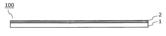
- FIG. 1 is a cross-sectional view illustrating a schematic configuration of an optical layered body according to an embodiment.
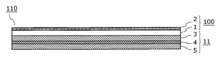
- FIG. 2 is a cross-sectional view illustrating a schematic configuration of the polarizing plate according to the embodiment.
- FIG. 3 is a cross-sectional view illustrating a schematic configuration of the display device according to the embodiment.
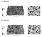
- FIG. 4 is a diagram showing the uneven shape on the surface of the optical functional layer of the optical layered body according to Example 5 and Comparative Example 5.
- FIG. 5 is a graph plotting the amount of resin particles added and the amount of colloidal silica added in Examples 1 to 13 and Comparative Examples 1 to 3, 7 and 8 shown in Table 2.
- FIG. 1 is a cross-sectional view showing a schematic configuration of an optical layered body according to an embodiment.
- the optical laminate 100 according to the embodiment includes a translucent substrate 1 and at least one optical functional layer 2 laminated on the translucent substrate 1. Fine irregularities are formed on the surface of the optical functional layer 2.
- the optical function layer 2 exhibits anti-glare properties by irregularly reflecting the diplomacy by the unevenness.
- polyethylene terephthalate PET
- triacetyl cellulose TAC
- polyethylene naphthalate PEN
- polymethyl methacrylate PMMA
- PC polycarbonate
- PI polyimide
- PE polypropylene
- resin films such as (PP), polyvinyl alcohol (PVA), polyvinyl chloride (PVC), cycloolefin copolymer (COC), norbornene resin, polyethersulfone, cellophane, and aromatic polyamide can be suitably used.
- the total light transmittance (JIS K7105) of the translucent substrate is preferably 80% or more, and more preferably 90% or more.
- the thickness of the translucent substrate is preferably 1 to 700 ⁇ m and more preferably 25 to 250 ⁇ m in view of the productivity and handling properties of the optical laminate.
- the translucent substrate is preferably subjected to a surface modification treatment in order to improve adhesion with the optical functional layer.
- a surface modification treatment include alkali treatment, corona treatment, plasma treatment, sputtering treatment, application of a surfactant and a silane coupling agent, Si deposition, and the like.
- the optical functional layer contains a base resin, resin particles (organic filler), and two types of inorganic fine particles.
- the optical functional layer is formed by applying a base resin that is cured by irradiation with ionizing radiation or ultraviolet rays, a resin composition in which resin particles and two kinds of inorganic fine particles are mixed, to a translucent substrate, and curing the coating film. Formed by.
- the base resin a resin that can be cured by irradiation with ionizing radiation or ultraviolet rays can be used.
- Resin materials that are cured by irradiation with ionizing radiation include radical polymerizable functional groups such as acryloyl group, methacryloyl group, acryloyloxy group, and methacryloyloxy group, and cationic polymerizable functional groups such as epoxy group, vinyl ether group, and oxetane group.
- radical polymerizable functional groups such as acryloyl group, methacryloyl group, acryloyloxy group, and methacryloyloxy group
- cationic polymerizable functional groups such as epoxy group, vinyl ether group, and oxetane group.
- Monomers, oligomers and prepolymers can be used alone or in admixture.
- Examples of the monomer include methyl acrylate, methyl methacrylate, methoxypolyethylene methacrylate, cyclohexyl methacrylate, phenoxyethyl methacrylate, ethylene glycol dimethacrylate, dipentaerythritol hexaacrylate, trimethylolpropane trimethacrylate, pentaerythritol triacrylate and the like.
- polyester acrylate polyurethane acrylate, polyfunctional urethane acrylate, epoxy acrylate, polyether acrylate, acrylate compounds such as alkit acrylate, melamine acrylate, silicone acrylate, unsaturated polyester, tetramethylene glycol diglycidyl ether, Epoxy compounds such as propylene glycol diglycidyl ether, neopentyl glycol diglycidyl ether, bisphenol A diglycidyl ether and various alicyclic epoxies, 3-ethyl-3-hydroxymethyloxetane, 1,4-bis ⁇ [((3- Oxeta such as ethyl-3-oxetanyl) methoxy] methyl ⁇ benzene, di [1-ethyl (3-oxetanyl)] methyl ether
- the compounds can be exemplified.
- Photopolymerization initiators include radical polymerization initiators such as acetophenone, benzophenone, thioxanthone, benzoin, and benzoin methyl ether, and cationic polymerization starts such as aromatic diazonium salts, aromatic sulfonium salts, aromatic iodonium salts, and metallocene compounds.
- the agents can be used alone or in combination.
- Resin particles added to the optical functional layer aggregate in the base resin to form a fine concavo-convex structure on the surface of the optical functional layer.
- the resin particles are made of a translucent resin material such as acrylic resin, polystyrene resin, styrene- (meth) acrylic acid ester copolymer, polyethylene resin, epoxy resin, silicone resin, polyvinylidene fluoride, and polyfluorinated ethylene resin. Things can be used.
- the refractive index of the resin particle material is preferably 1.40 to 1.75. In order to adjust the refractive index and dispersion of the resin particles, two or more kinds of resin particles having different materials (refractive index) may be mixed and used.
- the refractive index n f of the resin particles and the refractive index nz of the base resin preferably satisfy the following condition ( ⁇ ), and more preferably satisfy the following condition ( ⁇ ).
- refractive index n z of a resin material as a base material is not satisfied conditions (alpha), increasing the amount of resin particles to obtain the desired internal haze Necessary, and image sharpness deteriorates.
- the average particle size of the resin particles is preferably 0.3 to 10.0 ⁇ m, and more preferably 1.0 to 7.0 ⁇ m.
- the average particle diameter of the resin particles is less than 0.3 ⁇ m, the antiglare property decreases.
- the average particle diameter of the resin particles exceeds 10.0 ⁇ m, the area ratio of the uneven height on the surface of the optical functional layer cannot be controlled, and the glare resistance is deteriorated.
- the content of the resin particles in the solid content of the optical functional layer is 5.0 to 13.0%.
- the content of the resin particles is less than 5.0%, the unevenness of the surface of the optical functional layer is reduced and the antiglare property is lowered.
- the content of the resin particles exceeds 13.0%, the glare resistance decreases.
- the first inorganic fine particles and the second inorganic fine particles are added as two types of inorganic fine particles to the base resin of the optical functional layer.
- colloidal silica, alumina, and zinc oxide can be used alone or in combination.
- the first inorganic fine particles By adding the first inorganic fine particles, excessive aggregation of the resin particles can be suppressed, and the uneven structure formed on the surface of the optical functional layer can be made uniform, that is, locally increasing unevenness can be suppressed.
- the glare resistance By adding the first inorganic fine particles, the glare resistance can be improved while maintaining the antiglare property and the high contrast.
- the first inorganic fine particles are preferably inorganic nanoparticles having an average particle size of 10 to 100 nm.
- the average particle size is more preferably about 20 nm.
- alumina or zinc oxide is used as the first inorganic fine particles, the average particle size is about 40 nm. More preferably.
- the amount of the first inorganic fine particles added is preferably 0.05 to 10%, more preferably 0.1 to 3.0%, based on the total weight of the optical functional layer forming resin composition. . If the addition amount of the first inorganic fine particles is out of this range, the area ratio of the uneven height on the surface of the optical functional layer cannot be controlled, and the glare resistance deteriorates.
- the second inorganic fine particles are preferably inorganic nanoparticles having an average particle diameter of 10 to 200 nm.
- the addition amount of the second inorganic fine particles is preferably 0.1 to 5.0%.
- swellable clay can be used as the second inorganic fine particles.
- the swellable clay is not particularly limited as long as it has a cation exchange capacity and swells by taking in a solvent between the layers of the swellable clay, even if it is a natural product, it is a synthetic product (including substitution products and derivatives). May be.
- the mixture of a natural product and a synthetic product may be sufficient.
- swellable clay examples include mica, synthetic mica, vermiculite, montmorillonite, iron montmorillonite, beidellite, saponite, hectorite, stevensite, nontronite, magadiite, isallite, kanemite, layered titanic acid, smectite, and synthetic smectite. Etc. These swellable clays may be used alone or in combination.
- the layered organic clay refers to an organic onium ion introduced between the layers of the swellable clay.
- the organic onium ion is not limited as long as it can be organicized using the cation exchange property of the swellable clay.
- synthetic smectite layered organic clay mineral
- Synthetic smectite functions as a thickener that increases the viscosity of the optical functional layer forming resin composition. Addition of the synthetic smectite as a thickener suppresses the sedimentation of the resin particles and the first inorganic fine particles, and contributes to the formation of an uneven structure on the surface of the optical functional layer.
- the first inorganic fine particles and the second inorganic fine particles form aggregates in the optical functional layer.
- This agglomerate suppresses the aggregation of resin particles, and the unevenness height of the uneven shape on the surface of the optical functional layer is leveled, so that the scattering of light on the surface of the optical functional layer is made uniform and the glare resistance is improved. it can.
- a leveling agent may be added to the resin composition for forming the optical functional layer.
- the leveling agent has a function of being oriented on the surface of the coating film in the drying process, uniforming the surface tension of the coating film, and reducing surface defects of the coating film.
- an organic solvent may be appropriately added to the resin composition for forming the optical functional layer.
- the organic solvent include alcohols, esters, ketones, ethers, aromatic hydrocarbons and the like.
- the film thickness of the optical functional layer is preferably 1.0 to 12.0 ⁇ m, and more preferably 3.0 to 10.0 ⁇ m.
- the film thickness of the optical functional layer is less than 1 ⁇ m, curing failure due to oxygen inhibition occurs, and the scratch resistance of the optical functional layer tends to be lowered.
- the film thickness of the optical functional layer exceeds 12.0 ⁇ m, curling due to curing shrinkage of the base resin layer becomes strong, which is not preferable.
- the film thickness of the optical functional layer is preferably 100 to 140% of the average particle diameter of the resin particles, and more preferably 100 to 130% of the average particle diameter of the resin particles.
- the film thickness of the optical functional layer is less than 100% of the average particle diameter of the resin particles, the antiglare property with low whiteness and outstanding quality is obtained.
- the film thickness of the optical functional layer exceeds 140% of the average particle diameter of the resin particles, it becomes difficult to suppress the aggregation of the resin particles, resulting in insufficient glare resistance.
- the internal haze X and the total haze Y satisfy the following conditions (1) to (4) at the same time.
- the surface of the optical functional layer has large irregularities and the glare resistance is insufficient.
- the transmitted image definition of the optical layered body according to the present embodiment is 15 to 55% measured using an optical comb having a width of 0.5 mm.
- the transmitted image definition is less than 15%, the glare resistance is deteriorated.
- the transmitted image clarity exceeds 55%, the antiglare property deteriorates.
- the number of convex portions having a concavo-convex height of 0.1 ⁇ m or more is 900 or more per 1 mm 2 of the measurement area.
- the uneven height refers to the level difference between the concave and convex portions in the direction orthogonal to the measurement surface, based on the average level (height 0) of all the uneven heights on the measurement surface.
- the number of convex portions having a concavo-convex height of 0.1 ⁇ m or more is less than 900 per 1 mm 2 of the measurement area, the area occupied by one convex portion increases due to the aggregation of resin particles.
- an optical laminate is used as the antiglare film, the glare resistance is deteriorated.
- corrugated height is 0.7 micrometer or more is 60 or less per 1 mm ⁇ 2 > of measurement areas.
- the number of convex portions having an uneven height of 0.7 ⁇ m or more is 60 or less per 1 mm 2 of the measurement area, the number of locally uneven portions is reduced, and the glare resistance is improved.
- corrugated height is 0.1 micrometer or more is 310 micrometers 2 or less.
- the average area of the convex portions becomes small, and the convex portions Due to the uniform distribution, the glare resistance is improved.
- FIG. 2 is a cross-sectional view showing a schematic configuration of the polarizing plate according to the embodiment.
- the polarizing plate 110 includes the optical laminate 100 and the polarizing film 11.
- the optical laminated body 100 is shown in FIG. 1, and a polarizing film (polarizing substrate) 11 is provided on the surface of the translucent substrate 1 on which the optical functional layer 2 is not provided.
- the polarizing film 11 is obtained by, for example, laminating a transparent substrate 3, a polarizing layer 4, and a transparent substrate 5 in this order.
- the materials for the transparent substrates 3 and 5 and the polarizing layer 4 are not particularly limited, and those usually used for polarizing films can be used as appropriate.
- FIG. 3 is a cross-sectional view illustrating a schematic configuration of the display device according to the embodiment.
- the display device 120 is obtained by laminating the optical laminate 100, the polarizing film 11, the liquid crystal cell 13, the polarizing film (polarizing substrate) 12, and the backlight unit 14 in this order.
- the polarizing film 12 is obtained by, for example, laminating a transparent base material 6, a polarizing layer 7, and a transparent base material 8 in this order.
- the materials of the transparent substrates 6 and 8 and the polarizing layer 7 are not particularly limited, and those usually used for a polarizing film can be appropriately used.
- the liquid crystal cell 13 includes a liquid crystal panel in which liquid crystal molecules are sealed between a pair of transparent substrates having transparent electrodes, and a color filter, and changes the orientation of the liquid crystal molecules according to the voltage applied between the transparent electrodes. By controlling the light transmittance, the light transmittance of each pixel is controlled to form an image.
- the backlight unit 14 includes a light source and a light diffusing plate (both not shown), and is an illumination device that uniformly diffuses light emitted from the light source and emits it from the emission surface.
- the display device 120 illustrated in FIG. 3 may further include a diffusion film, a prism sheet, a brightness enhancement film, a retardation film for compensating for a retardation of a liquid crystal cell or a polarizing plate, and a touch sensor.
- the optical layered body according to the present embodiment further includes at least one layer of a refractive index adjusting layer such as a low refractive index layer, an antistatic layer, and an antifouling layer in addition to the optical functional layer for suppressing glare. Also good.
- a refractive index adjusting layer such as a low refractive index layer, an antistatic layer, and an antifouling layer in addition to the optical functional layer for suppressing glare. Also good.
- the low refractive index layer is a functional layer that is provided on the optical functional layer that suppresses glare and reduces the reflectance by reducing the refractive index of the surface.
- the low refractive index layer is formed by applying a coating solution containing an ionizing radiation curable material such as polyester acrylate monomer, epoxy acrylate monomer, urethane acrylate monomer, polyol acrylate monomer and a polymerization initiator, and polymerizing the coating film. It can be formed by curing.
- the low refractive particles include LiF, MgF, 3NaF.AlF or AlF (all with a refractive index of 1.4), or Na 3 AlF 6 (cryolite, with a refractive index of 1.33).
- Low refractive index fine particles made of a low refractive material such as the above may be dispersed.
- particles having voids inside the particles can be suitably used.
- the voids can be made to have a refractive index of air ( ⁇ 1), so that they can be low refractive index particles having a very low refractive index.
- the refractive index can be lowered by using low refractive index silica particles having voids inside.
- the antistatic layer is coated with a coating liquid containing an ionizing radiation curable material such as a polyester acrylate monomer, an epoxy acrylate monomer, a urethane acrylate monomer, a polyol acrylate monomer, a polymerization initiator, and an antistatic agent. It can be formed by curing by polymerization.
- an antistatic agent include antimony-doped tin oxide (ATO), metal oxide fine particles such as tin-doped indium oxide (ITO), polymer-type conductive compositions, and quaternary ammonium salts. Can be used.
- the antistatic layer may be provided on the outermost surface of the optical layered body, or may be provided between the optical functional layer that suppresses glare and the translucent substrate.
- the antifouling layer is provided on the outermost surface of the optical laminate and enhances the antifouling property by imparting water repellency and / or oil repellency to the optical laminate.
- the antifouling layer can be formed by dry coating or wet coating silicon oxide, fluorine-containing silane compound, fluoroalkylsilazane, fluoroalkylsilane, fluorine-containing silicon-based compound, perfluoropolyether group-containing silane coupling agent, etc. .
- antistatic layer and antifouling layer In addition to the low refractive index layer, antistatic layer and antifouling layer described above, or in addition to the low refractive index layer, antistatic layer and antifouling layer, at least an infrared absorbing layer, an ultraviolet absorbing layer, a color correction layer, etc.
- One layer may be provided.
- Base resin UV / EB curable resin
- Light acrylate PE-3A penentaerythritol triacrylate, manufactured by Kyoeisha Chemical Co., Ltd.
- Resin particles (organic filler) Cross-linked styrene monodisperse particles SX350H (manufactured by Soken Chemical Co., Ltd.), average particle size 3.50 ⁇ m, refractive index 1.595 Techpolymer SSX2035JXE (Sekisui Plastics Co., Ltd.), average particle size 3.35 ⁇ m, refractive index 1.565 Techpolymer SSX504 TNR (Sekisui Plastics Co., Ltd.), average particle size 3.60 ⁇ m, refractive index 1.555 Techpolymer XX-104CR (Sekisui Plastics Co., Ltd.), average particle size 3.50 ⁇ m, refractive index 1.595 Techpoly
- Colloidal silica Organosilica sol MEK-ST-40 (manufactured by Nissan Chemical Industries, Ltd.), average particle size of 10 to 15 nm ⁇
- Synthetic smectite Lucentite SAN (Coop Chemical Co., Ltd.)
- Fluorine-based leveling agent MegaFuck F-471 (manufactured by DIC Corporation) 0.1% ⁇
- Solvent Toluene
- Table 1 shows the composition of the resin particles used in Examples 1 to 13 and Comparative Examples 1 to 8.
- Table 2 shows the composition, coating thickness, haze value, transmitted image definition, and outermost surface of the optical functional layer of the optical functional layer forming coating solutions used in Examples 1 to 13 and Comparative Examples 1 to 8. The measured value of the number of the convex parts whose uneven
- the addition ratio of each component shown to Table 1 and 2 is a ratio (mass%) which occupies for the total solid content mass of the coating liquid for optical function layer formation.
- the total solid content of the coating solution for forming an optical functional layer refers to a component excluding the solvent. Therefore, the blending ratio (mass%) of the resin particles, the first inorganic fine particles, and the second inorganic fine particles in the total solid content of the coating liquid for forming the optical functional layer, and the cured film of the coating liquid for forming the optical functional layer
- the content ratio (% by mass) of the resin particles, the first inorganic fine particles, and the second inorganic fine particles in the optical functional layer is the same.
- Measurement methods for the film thickness, haze value, transmitted image definition, and number of convex portions having an uneven height of 0.1 ⁇ m or more present on the outermost surface of the optical functional layer are as follows.
- the film thickness of the optical functional layer was measured using a linear gauge (D-10HS, manufactured by Ozaki Manufacturing Co., Ltd.).
- the haze value was measured using a haze meter (NDH2000, manufactured by Nippon Denshoku Industries Co., Ltd.) according to JIS K7105.
- the haze value of the optical laminated film was defined as the total haze.
- the value obtained by subtracting the haze value of the transparent sheet with adhesive from the haze value measured by pasting the transparent sheet with adhesive on the surface provided with the fine uneven shape of the optical laminated film was defined as the internal haze.
- a polyethylene terephthalate film (thickness 38 ⁇ m) coated with an acrylic adhesive material (thickness 10 ⁇ m) was used as the transparent sheet with an adhesive material.
- the transmitted image definition was measured according to JIS K7105 using an image clarity measuring device (ICM-1T, manufactured by Suga Test Instruments Co., Ltd.) with an optical comb width of 0.5 mm.
- the unevenness of the outermost surface of the optical functional layer is determined by optical interference using a non-contact surface / layer cross-sectional shape measurement system (measuring device: Bart Scan R3300FL-Lite-AC, analysis software: VertScan4, manufactured by Ryoka System Co., Ltd.) Measured by the method.
- the measurement data was analyzed using the analysis software of the apparatus, and the number of convex portions having a concavo-convex height of 0.1 ⁇ m or more was measured with the analysis software.
- Table 3 shows the measurement conditions and analysis conditions of the measurement system.
- Antiglare properties, glare resistance, luminance ratio, and film thickness conditions were evaluated according to the following evaluation methods.
- Anti-glare property is 50 cm vertically from the center of the black acrylic plate after the optical laminates of the examples and comparative examples are bonded to a black acrylic plate (Sumipex 960, manufactured by Sumitomo Chemical Co., Ltd.) via a transparent adhesive layer.
- a black acrylic plate Silicon 960, manufactured by Sumitomo Chemical Co., Ltd.
- the presence / absence of reflection of his / her image (face) on a black acrylic plate when viewed from a distant place under the condition of illuminance of 250 lx was evaluated by visual judgment of arbitrary 100 people.
- the evaluation result was “ ⁇ ” when the number of people who did not feel the reflection was 70 or more, “ ⁇ ” when the number was 30 or more and less than 70, and “X” when the number was less than 30.
- the glare resistance is determined by the screen surface of the liquid crystal monitor (iPad3 (3rd generation) manufactured by Apple Incorporated, 264 ppi, “iPad” is a registered trademark) through the optical laminated body of each example and each comparative example through a transparent adhesive layer. After being bonded together, the liquid crystal monitor was put in a green display state, and the presence or absence of glare when the liquid crystal monitor was viewed from a location 50 cm vertically away from the center of the screen surface in a dark room was evaluated by visual judgment of any 100 people. . The evaluation results were “ ⁇ ” when the number of people who did not feel glare was 70 or more, “ ⁇ ” when the number was 30 or more and less than 70, and “X” when the number was less than 30.
- the luminance ratio is a liquid crystal monitor (iPad3 (3rd generation) manufactured by Apple Incorporated, 264ppi “iPad” is a registered trademark) through the optical laminate and the translucent substrate of each example and each comparative example through a transparent adhesive layer. After being pasted on the screen surface, the liquid crystal monitor was put in a white display state, and the luminance was measured with a spectroradiometer (SU-UL1R manufactured by Topcon Corporation) from a location 70 cm vertically away from the center of the screen surface in a dark room. . When the luminance of the translucent substrate is 100%, the case of 95% or more is “ ⁇ ”, and the case of less than 95% is “X”.
- the total haze (Y) and the internal haze (X) of the optical laminates according to Examples 1 to 13 satisfy all the conditional expressions (1) to (4) described above, and the transmitted image is clear.
- the degree was also in the range of 15 to 55%, and the number of convex portions with a concavo-convex height of 0.1 ⁇ m or more per 1 mm 2 of the measurement area was 900 or more. Therefore, the optical laminates according to Examples 1 to 13 were all excellent in glare resistance, antiglare property and luminance ratio.
- FIG. 4 shows the optical laminate according to Example 5 and Comparative Example 5 measured by the optical interference method using the non-contact surface / layer cross-sectional shape measurement system described above, and the uneven shape on the surface of the optical functional layer was output as an image.
- the image shown in the left column of FIG. 4 is obtained by outputting the uneven shape on the surface of the optical function layer as a three-dimensional image, and the dark portion corresponds to the portion where the unevenness is large with respect to the reference surface.
- the image shown in the right column of FIG. 4 is an image showing the distribution of convex portions with an uneven height of 0.1 ⁇ m or more on the surface of the optical functional layer, and the dark and light portions have an uneven height of 0.1 ⁇ m or more. Represents a convex part. 4A and 4B correspond to Example 5 and Comparative Example 5, respectively.
- the area of each convex portion decreases and the distribution of the convex portions becomes uniform.
- the area of each convex portion increases, so that locally large portions (dark portions in FIG. 4) may increase.
- the number of convex portions having a concavo-convex height of 0.1 ⁇ m or more is 900 or more per 1 mm 2 of the measurement area, so that the convex portions are not localized and uniform. As a result, the glare resistance is considered to be improved.
- Table 4 classifies the number of convex portions on the surface of the optical laminates according to Examples 1, 4 to 10, 13 and Comparative Examples 4, 5, and 8 for each height threshold.
- the number of convex portions having a concavo-convex height equal to or higher than the value described in the height threshold column among the convex portions formed on the surface of the optical laminate is shown.
- Table 5 shows the area distribution of the convex portions formed on the surface of the optical laminates according to Examples 1, 4 to 10, 13 and Comparative Examples 4, 5, and 8, and the average area of the convex portions.
- the numerical value of the area distribution in Table 5 is obtained by measuring the area of a convex portion having a height of 0.1 ⁇ m or more existing within a predetermined reference area using the non-contact surface / layer cross-sectional shape measurement system described above, and is 100 ⁇ m 2 .
- the frequency of appearance is tabulated for each area range.
- “a to b” in the area range means “a” to “b”.
- the area range “0 to 100” means 0 or more and less than 100.
- the average area of Table 5 was calculated from these measured values by measuring the area and number of convex portions having a height of 0.1 ⁇ m or more using the non-contact surface / layer cross-sectional shape measurement system described above. is there.
- the average area of all the convex portions having the uneven height of 0.1 ⁇ m or more is 310 ⁇ m 2 or less.
- the average area of all the convex portions having the uneven height of 0.1 ⁇ m or more is larger than 310 ⁇ m 2 .
- FIG. 5 is a graph plotting the amount of resin particles added and the amount of colloidal silica added in Examples 1 to 13 and Comparative Examples 1 to 3, 7 and 8 shown in Table 2.
- the examples are plotted with black circles, and the comparative examples are plotted with crosses.
- the plots of the addition amount of the resin particles and the addition amount of colloidal silica in Examples 1 to 13 are regions below the straight line shown by the broken line in FIG. 5 (except on the horizontal axis).
- the amount of the resin particles is in the range of 5.0 to 13.0%, even when used as an antiglare film for a high-definition image display device of 200 ppi or more, It was confirmed that excellent performance can be obtained in all of the antiglare property and contrast. That is, when the resin particle content in the optical functional layer forming resin composition is A (%) and the colloidal silica content is B (%), the following conditional expressions (5) and (6) are satisfied.
- conditional expression (5) is a straight line that passes through both the plots of the addition amount of the resin particles and the addition amount of colloidal silica in Examples 2 and 14. 0 ⁇ B ⁇ 0.313A ⁇ 1.06 (5) 5.0 ⁇ A ⁇ 13.0 (6)
- the optical laminates according to Examples 1 to 13 are used as an antiglare film for a high-definition image display device of 200 ppi or more, the optical laminates have a glare resistance, an antiglare resistance and a contrast. It was confirmed that excellent performance can be exhibited in all.
- optical laminate according to the present invention can be used as an antiglare film for use in a high-definition (for example, 200 ppi or more) image display device.
Landscapes
- Physics & Mathematics (AREA)
- General Physics & Mathematics (AREA)
- Optics & Photonics (AREA)
- Nonlinear Science (AREA)
- Chemical & Material Sciences (AREA)
- Engineering & Computer Science (AREA)
- Crystallography & Structural Chemistry (AREA)
- Mathematical Physics (AREA)
- Chemical Kinetics & Catalysis (AREA)
- Theoretical Computer Science (AREA)
- Optical Elements Other Than Lenses (AREA)
- Laminated Bodies (AREA)
- Polarising Elements (AREA)
- Devices For Indicating Variable Information By Combining Individual Elements (AREA)
- Liquid Crystal (AREA)
- Surface Treatment Of Optical Elements (AREA)
Abstract
Priority Applications (4)
| Application Number | Priority Date | Filing Date | Title |
|---|---|---|---|
| KR1020187023107A KR101943810B1 (ko) | 2016-02-16 | 2017-02-14 | 광학 적층체, 편광판 및 표시 장치 |
| JP2017531798A JP6221018B1 (ja) | 2016-02-16 | 2017-02-14 | 光学積層体、偏光板及び表示装置 |
| CN201780011162.7A CN108603954B (zh) | 2016-02-16 | 2017-02-14 | 光学层叠体、偏光板及显示装置 |
| US16/058,891 US10591644B2 (en) | 2016-02-16 | 2018-08-08 | Optical laminate, polarizer, and display apparatus |
Applications Claiming Priority (2)
| Application Number | Priority Date | Filing Date | Title |
|---|---|---|---|
| JP2016027340 | 2016-02-16 | ||
| JP2016-027340 | 2016-02-16 |
Related Child Applications (1)
| Application Number | Title | Priority Date | Filing Date |
|---|---|---|---|
| US16/058,891 Continuation US10591644B2 (en) | 2016-02-16 | 2018-08-08 | Optical laminate, polarizer, and display apparatus |
Publications (1)
| Publication Number | Publication Date |
|---|---|
| WO2017141903A1 true WO2017141903A1 (fr) | 2017-08-24 |
Family
ID=59625937
Family Applications (1)
| Application Number | Title | Priority Date | Filing Date |
|---|---|---|---|
| PCT/JP2017/005308 WO2017141903A1 (fr) | 2016-02-16 | 2017-02-14 | Stratifié optique, plaque polarisante, et dispositif d'affichage |
Country Status (6)
| Country | Link |
|---|---|
| US (1) | US10591644B2 (fr) |
| JP (1) | JP6221018B1 (fr) |
| KR (1) | KR101943810B1 (fr) |
| CN (1) | CN108603954B (fr) |
| TW (1) | TWI623797B (fr) |
| WO (1) | WO2017141903A1 (fr) |
Cited By (8)
| Publication number | Priority date | Publication date | Assignee | Title |
|---|---|---|---|---|
| JP2019105694A (ja) * | 2017-12-11 | 2019-06-27 | 株式会社ダイセル | 防眩フィルム並びにその製造方法及び用途 |
| JP2019168667A (ja) * | 2018-03-21 | 2019-10-03 | 立景光電股▲ふん▼有限公司 | 表示パネル及び表示パネルを製造する方法 |
| WO2019221000A1 (fr) * | 2018-05-15 | 2019-11-21 | 株式会社ポラテクノ | Composition de résine photosensible et film antireflet |
| EP3734332A4 (fr) * | 2018-05-11 | 2021-02-17 | Lg Chem, Ltd. | Film antireflet et appareil d'affichage |
| WO2021095746A1 (fr) * | 2019-11-11 | 2021-05-20 | 日東電工株式会社 | Film antireflet ainsi que procédés de conception et de fabrication de celui-ci, élément optique, dispositif d'affichage d'image |
| WO2021095745A1 (fr) * | 2019-11-11 | 2021-05-20 | 日東電工株式会社 | Film antireflet ainsi que procédés de conception et de fabrication de celui-ci, élément optique, dispositif d'affichage d'image |
| JP2021525395A (ja) * | 2019-01-14 | 2021-09-24 | エルジー・ケム・リミテッド | 偏光板、およびディスプレイ装置 |
| EP3754387A4 (fr) * | 2018-11-15 | 2021-11-17 | Lg Chem, Ltd. | Stratifié optique, plaque polarisante et dispositif d'affichage |
Families Citing this family (3)
| Publication number | Priority date | Publication date | Assignee | Title |
|---|---|---|---|---|
| TWI652167B (zh) | 2016-02-10 | 2019-03-01 | 凸版巴川光學薄膜股份有限公司 | 光學積層體、偏光板及顯示裝置 |
| JP7286269B2 (ja) * | 2018-03-23 | 2023-06-05 | 恵和株式会社 | バックライトユニット |
| JP2020056921A (ja) * | 2018-10-02 | 2020-04-09 | 凸版印刷株式会社 | 湿度応答性可逆変形構造体及びその製造方法 |
Citations (4)
| Publication number | Priority date | Publication date | Assignee | Title |
|---|---|---|---|---|
| JP2005300576A (ja) * | 2004-04-06 | 2005-10-27 | Konica Minolta Opto Inc | 防眩性反射防止フィルム、偏光板及び表示装置 |
| JP2007045142A (ja) * | 2005-02-22 | 2007-02-22 | Fujifilm Corp | 防眩性フィルム、反射防止フィルム、その製造方法、該フィルムを用いた偏光板および該偏光板を用いた液晶表示装置 |
| JP2008292987A (ja) * | 2007-04-24 | 2008-12-04 | Tomoegawa Paper Co Ltd | 光学積層体 |
| JP5066535B2 (ja) * | 2007-01-31 | 2012-11-07 | 株式会社巴川製紙所 | 光学積層フィルム |
Family Cites Families (16)
| Publication number | Priority date | Publication date | Assignee | Title |
|---|---|---|---|---|
| US7166656B2 (en) | 2001-11-13 | 2007-01-23 | Eastman Kodak Company | Smectite clay intercalated with polyether block polyamide copolymer |
| US6767952B2 (en) | 2001-11-13 | 2004-07-27 | Eastman Kodak Company | Article utilizing block copolymer intercalated clay |
| TW200641387A (en) | 2005-02-21 | 2006-12-01 | Dainippon Printing Co Ltd | Anti-glare optical multilayer body |
| US20080137206A1 (en) | 2005-02-22 | 2008-06-12 | Fujifilm Corporation | Film, Manufacturing Method Thereof, Polarization Plate Using the Film, and Liquid Crystal, and Display Device Using the Polarizing Plate |
| US8057907B2 (en) | 2006-03-06 | 2011-11-15 | Fujifilm Corporation | Optical film, coating composition, polarizing plate and image display device |
| US20100246011A1 (en) | 2006-03-29 | 2010-09-30 | Tomoegawa Co., Ltd. | Optical film |
| US8778489B2 (en) * | 2007-03-31 | 2014-07-15 | Tomoegawa Co., Ltd. | Optical layered product |
| JP2008276205A (ja) * | 2007-03-31 | 2008-11-13 | Tomoegawa Paper Co Ltd | 光学積層体 |
| JP5525886B2 (ja) * | 2009-03-30 | 2014-06-18 | 富士フイルム株式会社 | 防眩フィルムの製造方法、防眩フィルム、偏光板、画像表示装置及び透過型/半透過型液晶表示装置 |
| US8325296B2 (en) | 2009-03-30 | 2012-12-04 | Fujifilm Corporation | Light-transmitting substrate, optical film, polarizing plate and image display device |
| JP5008734B2 (ja) * | 2010-03-18 | 2012-08-22 | 大日本印刷株式会社 | 防眩性フィルム、防眩性フィルムの製造方法、偏光板及び画像表示装置 |
| WO2011135853A1 (fr) * | 2010-04-27 | 2011-11-03 | 株式会社巴川製紙所 | Stratifié optique, plaque de polarisation et dispositif d'affichage |
| JP2011232683A (ja) | 2010-04-30 | 2011-11-17 | Tomoegawa Paper Co Ltd | 光学積層体、偏光板および表示装置 |
| JP5974894B2 (ja) * | 2010-10-22 | 2016-08-23 | 大日本印刷株式会社 | 防眩性フィルム、偏光板及び画像表示装置 |
| CA3185265A1 (fr) * | 2014-10-02 | 2016-04-07 | Ventana Medical Systems, Inc. | Polymeres et conjugues comprenant ces polymeres |
| TWI652167B (zh) | 2016-02-10 | 2019-03-01 | 凸版巴川光學薄膜股份有限公司 | 光學積層體、偏光板及顯示裝置 |
-
2017
- 2017-02-14 CN CN201780011162.7A patent/CN108603954B/zh active Active
- 2017-02-14 JP JP2017531798A patent/JP6221018B1/ja active Active
- 2017-02-14 KR KR1020187023107A patent/KR101943810B1/ko active IP Right Grant
- 2017-02-14 WO PCT/JP2017/005308 patent/WO2017141903A1/fr active Application Filing
- 2017-02-14 TW TW106104695A patent/TWI623797B/zh active
-
2018
- 2018-08-08 US US16/058,891 patent/US10591644B2/en active Active
Patent Citations (4)
| Publication number | Priority date | Publication date | Assignee | Title |
|---|---|---|---|---|
| JP2005300576A (ja) * | 2004-04-06 | 2005-10-27 | Konica Minolta Opto Inc | 防眩性反射防止フィルム、偏光板及び表示装置 |
| JP2007045142A (ja) * | 2005-02-22 | 2007-02-22 | Fujifilm Corp | 防眩性フィルム、反射防止フィルム、その製造方法、該フィルムを用いた偏光板および該偏光板を用いた液晶表示装置 |
| JP5066535B2 (ja) * | 2007-01-31 | 2012-11-07 | 株式会社巴川製紙所 | 光学積層フィルム |
| JP2008292987A (ja) * | 2007-04-24 | 2008-12-04 | Tomoegawa Paper Co Ltd | 光学積層体 |
Cited By (13)
| Publication number | Priority date | Publication date | Assignee | Title |
|---|---|---|---|---|
| JP2019105694A (ja) * | 2017-12-11 | 2019-06-27 | 株式会社ダイセル | 防眩フィルム並びにその製造方法及び用途 |
| US11772365B2 (en) | 2017-12-11 | 2023-10-03 | Daicel Corporation | Anti-glare film, method for producing same, and use of same |
| JP2019168667A (ja) * | 2018-03-21 | 2019-10-03 | 立景光電股▲ふん▼有限公司 | 表示パネル及び表示パネルを製造する方法 |
| US10514571B2 (en) | 2018-03-21 | 2019-12-24 | Himax Display, Inc. | Display panel and method of fabricating a display panel |
| EP3734332A4 (fr) * | 2018-05-11 | 2021-02-17 | Lg Chem, Ltd. | Film antireflet et appareil d'affichage |
| JP2021513109A (ja) * | 2018-05-11 | 2021-05-20 | エルジー・ケム・リミテッド | 防眩フィルムおよびディスプレイ装置 |
| JP7134549B2 (ja) | 2018-05-11 | 2022-09-12 | エルジー・ケム・リミテッド | 防眩フィルムおよびディスプレイ装置 |
| WO2019221000A1 (fr) * | 2018-05-15 | 2019-11-21 | 株式会社ポラテクノ | Composition de résine photosensible et film antireflet |
| EP3754387A4 (fr) * | 2018-11-15 | 2021-11-17 | Lg Chem, Ltd. | Stratifié optique, plaque polarisante et dispositif d'affichage |
| JP2021525395A (ja) * | 2019-01-14 | 2021-09-24 | エルジー・ケム・リミテッド | 偏光板、およびディスプレイ装置 |
| CN114651197A (zh) * | 2019-11-11 | 2022-06-21 | 日东电工株式会社 | 防眩性膜、防眩性膜的设计方法、防眩性膜的制造方法、光学构件及影像显示设备 |
| WO2021095745A1 (fr) * | 2019-11-11 | 2021-05-20 | 日東電工株式会社 | Film antireflet ainsi que procédés de conception et de fabrication de celui-ci, élément optique, dispositif d'affichage d'image |
| WO2021095746A1 (fr) * | 2019-11-11 | 2021-05-20 | 日東電工株式会社 | Film antireflet ainsi que procédés de conception et de fabrication de celui-ci, élément optique, dispositif d'affichage d'image |
Also Published As
| Publication number | Publication date |
|---|---|
| CN108603954A (zh) | 2018-09-28 |
| TW201732396A (zh) | 2017-09-16 |
| CN108603954B (zh) | 2019-12-13 |
| JPWO2017141903A1 (ja) | 2018-02-22 |
| JP6221018B1 (ja) | 2017-10-25 |
| US10591644B2 (en) | 2020-03-17 |
| KR101943810B1 (ko) | 2019-01-29 |
| US20180348408A1 (en) | 2018-12-06 |
| TWI623797B (zh) | 2018-05-11 |
| KR20180099883A (ko) | 2018-09-05 |
Similar Documents
| Publication | Publication Date | Title |
|---|---|---|
| JP6221018B1 (ja) | 光学積層体、偏光板及び表示装置 | |
| JP6698552B2 (ja) | 光学積層体、偏光板及び表示装置 | |
| JP6221017B1 (ja) | 光学積層体、偏光板及び表示装置 | |
| KR102026541B1 (ko) | 광학 적층체, 편광판 및 표시 장치 | |
| KR102194639B1 (ko) | 광학 적층체, 편광판 및 표시 장치 | |
| WO2020100958A1 (fr) | Film antireflet, son procédé de fabrication, élément optique et dispositif d'affichage d'image | |
| TWI834758B (zh) | 防眩性薄膜、防眩性薄膜之製造方法、光學構件及影像顯示裝置 |
Legal Events
| Date | Code | Title | Description |
|---|---|---|---|
| ENP | Entry into the national phase |
Ref document number: 2017531798 Country of ref document: JP Kind code of ref document: A |
|
| 121 | Ep: the epo has been informed by wipo that ep was designated in this application |
Ref document number: 17753160 Country of ref document: EP Kind code of ref document: A1 |
|
| ENP | Entry into the national phase |
Ref document number: 20187023107 Country of ref document: KR Kind code of ref document: A |
|
| WWE | Wipo information: entry into national phase |
Ref document number: 1020187023107 Country of ref document: KR |
|
| NENP | Non-entry into the national phase |
Ref country code: DE |
|
| 122 | Ep: pct application non-entry in european phase |
Ref document number: 17753160 Country of ref document: EP Kind code of ref document: A1 |