WO2017138241A1 - 積層トランス及び積層トランス製造方法 - Google Patents
積層トランス及び積層トランス製造方法 Download PDFInfo
- Publication number
- WO2017138241A1 WO2017138241A1 PCT/JP2016/086911 JP2016086911W WO2017138241A1 WO 2017138241 A1 WO2017138241 A1 WO 2017138241A1 JP 2016086911 W JP2016086911 W JP 2016086911W WO 2017138241 A1 WO2017138241 A1 WO 2017138241A1
- Authority
- WO
- WIPO (PCT)
- Prior art keywords
- coil
- pattern
- layer
- magnetic
- patterns
- Prior art date
- Legal status (The legal status is an assumption and is not a legal conclusion. Google has not performed a legal analysis and makes no representation as to the accuracy of the status listed.)
- Ceased
Links
Images





Classifications
-
- H—ELECTRICITY
- H01—ELECTRIC ELEMENTS
- H01F—MAGNETS; INDUCTANCES; TRANSFORMERS; SELECTION OF MATERIALS FOR THEIR MAGNETIC PROPERTIES
- H01F27/00—Details of transformers or inductances, in general
- H01F27/28—Coils; Windings; Conductive connections
- H01F27/2804—Printed windings
-
- H—ELECTRICITY
- H01—ELECTRIC ELEMENTS
- H01F—MAGNETS; INDUCTANCES; TRANSFORMERS; SELECTION OF MATERIALS FOR THEIR MAGNETIC PROPERTIES
- H01F17/00—Fixed inductances of the signal type
- H01F17/0006—Printed inductances
- H01F17/0013—Printed inductances with stacked layers
-
- H—ELECTRICITY
- H01—ELECTRIC ELEMENTS
- H01F—MAGNETS; INDUCTANCES; TRANSFORMERS; SELECTION OF MATERIALS FOR THEIR MAGNETIC PROPERTIES
- H01F17/00—Fixed inductances of the signal type
- H01F17/04—Fixed inductances of the signal type with magnetic core
-
- H—ELECTRICITY
- H01—ELECTRIC ELEMENTS
- H01F—MAGNETS; INDUCTANCES; TRANSFORMERS; SELECTION OF MATERIALS FOR THEIR MAGNETIC PROPERTIES
- H01F27/00—Details of transformers or inductances, in general
- H01F27/24—Magnetic cores
-
- H—ELECTRICITY
- H01—ELECTRIC ELEMENTS
- H01F—MAGNETS; INDUCTANCES; TRANSFORMERS; SELECTION OF MATERIALS FOR THEIR MAGNETIC PROPERTIES
- H01F41/00—Apparatus or processes specially adapted for manufacturing or assembling magnets, inductances or transformers; Apparatus or processes specially adapted for manufacturing materials characterised by their magnetic properties
- H01F41/02—Apparatus or processes specially adapted for manufacturing or assembling magnets, inductances or transformers; Apparatus or processes specially adapted for manufacturing materials characterised by their magnetic properties for manufacturing cores, coils, or magnets
- H01F41/04—Apparatus or processes specially adapted for manufacturing or assembling magnets, inductances or transformers; Apparatus or processes specially adapted for manufacturing materials characterised by their magnetic properties for manufacturing cores, coils, or magnets for manufacturing coils
- H01F41/041—Printed circuit coils
-
- H—ELECTRICITY
- H01—ELECTRIC ELEMENTS
- H01F—MAGNETS; INDUCTANCES; TRANSFORMERS; SELECTION OF MATERIALS FOR THEIR MAGNETIC PROPERTIES
- H01F41/00—Apparatus or processes specially adapted for manufacturing or assembling magnets, inductances or transformers; Apparatus or processes specially adapted for manufacturing materials characterised by their magnetic properties
- H01F41/02—Apparatus or processes specially adapted for manufacturing or assembling magnets, inductances or transformers; Apparatus or processes specially adapted for manufacturing materials characterised by their magnetic properties for manufacturing cores, coils, or magnets
- H01F41/04—Apparatus or processes specially adapted for manufacturing or assembling magnets, inductances or transformers; Apparatus or processes specially adapted for manufacturing materials characterised by their magnetic properties for manufacturing cores, coils, or magnets for manufacturing coils
- H01F41/041—Printed circuit coils
- H01F41/043—Printed circuit coils by thick film techniques
-
- H—ELECTRICITY
- H01—ELECTRIC ELEMENTS
- H01F—MAGNETS; INDUCTANCES; TRANSFORMERS; SELECTION OF MATERIALS FOR THEIR MAGNETIC PROPERTIES
- H01F41/00—Apparatus or processes specially adapted for manufacturing or assembling magnets, inductances or transformers; Apparatus or processes specially adapted for manufacturing materials characterised by their magnetic properties
- H01F41/02—Apparatus or processes specially adapted for manufacturing or assembling magnets, inductances or transformers; Apparatus or processes specially adapted for manufacturing materials characterised by their magnetic properties for manufacturing cores, coils, or magnets
- H01F41/04—Apparatus or processes specially adapted for manufacturing or assembling magnets, inductances or transformers; Apparatus or processes specially adapted for manufacturing materials characterised by their magnetic properties for manufacturing cores, coils, or magnets for manufacturing coils
- H01F41/041—Printed circuit coils
- H01F41/046—Printed circuit coils structurally combined with ferromagnetic material
-
- H—ELECTRICITY
- H01—ELECTRIC ELEMENTS
- H01F—MAGNETS; INDUCTANCES; TRANSFORMERS; SELECTION OF MATERIALS FOR THEIR MAGNETIC PROPERTIES
- H01F17/00—Fixed inductances of the signal type
- H01F17/0006—Printed inductances
- H01F17/0013—Printed inductances with stacked layers
- H01F2017/002—Details of via holes for interconnecting the layers
-
- H—ELECTRICITY
- H01—ELECTRIC ELEMENTS
- H01F—MAGNETS; INDUCTANCES; TRANSFORMERS; SELECTION OF MATERIALS FOR THEIR MAGNETIC PROPERTIES
- H01F27/00—Details of transformers or inductances, in general
- H01F27/28—Coils; Windings; Conductive connections
- H01F27/2804—Printed windings
- H01F2027/2809—Printed windings on stacked layers
-
- H—ELECTRICITY
- H01—ELECTRIC ELEMENTS
- H01F—MAGNETS; INDUCTANCES; TRANSFORMERS; SELECTION OF MATERIALS FOR THEIR MAGNETIC PROPERTIES
- H01F27/00—Details of transformers or inductances, in general
- H01F27/28—Coils; Windings; Conductive connections
- H01F27/2804—Printed windings
- H01F2027/2819—Planar transformers with printed windings, e.g. surrounded by two cores and to be mounted on printed circuit
Definitions
- the present invention relates to a laminated transformer and a laminated transformer manufacturing method.
- transformers for example, generally have a structure in which a coil is wound around a magnetic core, so that it is difficult to reduce the size, and it is particularly difficult to reduce the height. Therefore, in recent years, a transformer having a laminated structure (that is, a laminated transformer) has been developed in order to reduce the size and the height.
- the disclosed technology has been made in view of the above, and an object of the present invention is to provide a laminated transformer having high coupling between a primary coil and a secondary coil.
- the laminated transformer has a magnetic layer and a coil layer.
- the coil layer is laminated on the magnetic layer. Inside the coil layer, there are formed a primary coil that circulates spirally while being superimposed in the stacking direction, and a secondary coil that circulates spirally while being superimposed in the stacking direction.
- the secondary coil is formed inside the primary coil.
- the inner side of the secondary coil is filled with a magnetic material.
- the space between the primary coil and the secondary coil and the outside of the primary coil are filled with a nonmagnetic material.
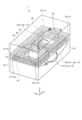
- FIG. 1 is a diagram illustrating an example of a structure of a laminated transformer according to an embodiment.
- FIG. 2 is an exploded perspective view of the laminated transformer of one embodiment.
- FIG. 3 is a diagram illustrating an example of a print pattern according to an embodiment.
- FIG. 4 is a diagram illustrating an example of a print pattern according to an embodiment.
- FIG. 5 is a diagram illustrating an example of a print pattern according to an embodiment.
- FIG. 6 is a diagram illustrating an example of a print pattern according to an embodiment.
- FIG. 7 is a diagram illustrating an example of a print pattern according to an embodiment.
- FIG. 8 is a diagram illustrating an example of a printing pattern according to an embodiment.
- FIG. 9 is a diagram illustrating an example of a print pattern according to an embodiment.
- FIG. 10 is a diagram illustrating an example of a printing pattern according to an embodiment.
- FIG. 11 is a diagram illustrating an example of a print pattern according to an embodiment.
- FIG. 1 is a diagram illustrating an example of a structure of a laminated transformer according to an embodiment.
- the laminated transformer 1 shown in FIG. 1 includes magnetic layers 15-1 and 15-2 and a coil layer 10.
- the magnetic layers 15-1 and 15-2 and the coil layer 10 are stacked on each other with the coil layer 10 sandwiched between the magnetic layer 15-1 and the magnetic layer 15-2.
- the magnetic layer 15-1 and the magnetic layer 15-2 may be collectively referred to as the magnetic layer 15 unless they are particularly distinguished.
- the material of the magnetic layer 15 is, for example, magnetic ferrite.
- a primary coil C1 that spirally circulates while being superimposed in the Z direction (that is, the stacking direction) is formed.
- a secondary coil C ⁇ b> 2 that spirals around in the Z direction is formed inside the coil layer 10.
- two primary coils C1 are formed side by side in the X direction
- two secondary coils C2 are formed side by side in the X direction.
- the two primary coils C1 arranged in the X direction are connected, for example, near the middle of the coil layer 10 in the Z direction.
- the two secondary coils C2 arranged in the X direction are connected to each other at the lowermost portion of the coil layer 10 in the Z direction, for example.
- the material of the primary coil C1 and the secondary coil C2 is silver, for example.
- the winding direction of the primary coil C1 and the winding direction of the secondary coil C2 are opposite to each other. Moreover, in the location where the primary coil C1 exists in the coil layer 10, the secondary coil C2 is formed inside the primary coil C1.
- the input end C1-in of the primary coil C1 and the input end C2-in of the secondary coil C2 are provided, for example, on any one of the four side surfaces of the coil layer 10.
- the output end C1-out of the primary coil C1 and the output end C2-out of the secondary coil C2 are, for example, side surfaces provided with the input ends C1-in and C2-in among the four side surfaces of the coil layer 10. Are provided on the same side surface facing each other.
- the inside of the secondary coil C ⁇ b> 2 is filled with the magnetic body 20.
- the material of the magnetic body 20 filled inside the secondary coil C2 is, for example, magnetic ferrite.
- the space between the primary coil C1 and the secondary coil C2 is filled with a nonmagnetic material 25.
- the outside of the primary coil C ⁇ b> 1 is also filled with the nonmagnetic material 25.
- the outer side of the primary coil C ⁇ b> 1 is filled with the nonmagnetic material 25, whereby the side surface of the coil layer 10 is formed with the nonmagnetic material 25.
- the material of the nonmagnetic material 25 is, for example, nonmagnetic ferrite.
- Such a coil layer 10 is prepared in accordance with ⁇ Laminated transformer manufacturing method> described below.
- first region a region between the primary coil C1 and the secondary coil C2 (hereinafter sometimes referred to as “first region”) and a region outside the primary coil C1 (hereinafter referred to as “first”).
- first region a region between the primary coil C1 and the secondary coil C2
- first region a region outside the primary coil C1
- second region a region outside the primary coil C1
- the “minor loop” which is an unnecessary magnetic flux that circulates in the laminated transformer 1 through the outside of the primary coil C1 and the secondary coil C2 is caused by the nonmagnetic material 25 filled in the first region and the second region. Blocked. That is, by filling the first region and the second region with the nonmagnetic material 25, the occurrence of minor loops can be prevented.
- the minor loop becomes a disturbance to the main loop and becomes a factor of reducing the coupling between the primary coil C1 and the secondary coil C2. Therefore, by preventing the occurrence of the minor loop, the coupling between the primary coil C1 and the secondary coil C2 can be increased compared to when the minor loop is generated.
- FIG. 2 is an exploded perspective view of the laminated transformer of one embodiment.
- the coil layer 10 includes a plurality of layers from the L1 layer that forms the lowermost surface of the coil layer 10 to the L10 layer that forms the uppermost surface of the coil layer 10. . That is, the coil layer 10 has a laminated structure in which the layers from the L1 layer to the L10 layer are sequentially laminated in the Z direction. The L1 to L10 layers have the same thickness.
- the laminated transformer 1 has a laminated structure in which the magnetic layer 15-1, the coil layer 10, and the magnetic layer 15-2 are sequentially laminated in the Z direction. When the laminated transformer 1 is viewed in the thickness direction (that is, the Z direction), the L1 to L10 layers have the same thickness.
- the nonmagnetic material 25 filled on the outside of the primary coil C1 is formed by screen printing as a coil pattern (that is, a conductor pattern), a magnetic pattern, and a nonmagnetic pattern as follows. Therefore, each of the L1 to L10 layers corresponds to a “printed pattern layer” formed by screen-printing a coil pattern, a magnetic pattern, and a nonmagnetic pattern.
- These print pattern layers are laminated on the magnetic layer 15-1 as shown in FIG.
- the coil pattern is formed by screen printing of paste-like silver
- the magnetic pattern is formed by screen printing of paste-like magnetic ferrite
- the non-magnetic pattern is formed by screen printing of paste-like non-magnetic ferrite.
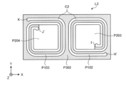
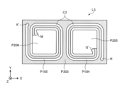
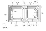
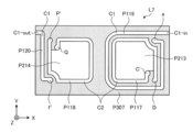
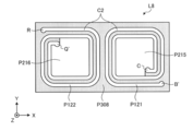
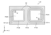
- FIGS. 3 to 12 are diagrams showing an example of a printing pattern according to an embodiment.
- the layers L1 to L10 shown in FIGS. 3 to 12 are screen-printed on the magnetic layer 15-1 in order from the L1 layer. That is, the L1 layer corresponds to the lowermost layer of the coil layer 10, and the L10 layer corresponds to the uppermost layer of the coil layer 10.
- the L1 layer is formed by screen printing a coil pattern P101, magnetic patterns P201 and P202, and a nonmagnetic pattern P301.
- the coil pattern P101 is a coil pattern of the secondary coil C2.
- magnetic patterns P201 and P202 are formed in all regions inside the coil pattern P101, and nonmagnetic patterns P301 are formed in all regions other than the coil pattern P101 and the magnetic patterns P201 and P202.
- two secondary coils C2 arranged in the X direction are connected to each other.
- the magnetic patterns P201 and P202 and the nonmagnetic pattern P301 have the same thickness as the L1 layer, and the coil pattern P101 is thinner than the L1 layer.
- the upper surface of the coil pattern P101, the upper surfaces of the magnetic patterns P201 and P202, and the upper surface of the nonmagnetic pattern P301 coincide with each other.
- the L2 layer is formed by screen printing coil patterns P102 and P103, magnetic patterns P203 and P204, and nonmagnetic pattern P302.
- the coil patterns P102 and P103 are coil patterns of the secondary coil C2.
- the magnetic pattern P203 is formed in all the regions inside the coil pattern P102
- the magnetic pattern P204 is formed in all the regions inside the coil pattern P103, except for the coil patterns P102 and P103 and the magnetic patterns P203 and P204.
- a nonmagnetic pattern P302 is formed in all the regions.
- the magnetic patterns P203 and P204 and the nonmagnetic pattern P302 have the same thickness as the L2 layer, and the coil patterns P102 and P103 are thinner than the L2 layer. Further, the upper surfaces of the coil patterns P102 and P103, the upper surfaces of the magnetic patterns P203 and P204, and the upper surface of the nonmagnetic pattern P302 coincide with each other.
- the L3 layer is formed by screen printing coil patterns P104 and P105, magnetic patterns P205 and P206, and nonmagnetic pattern P303.
- the coil patterns P104 and P105 are coil patterns of the secondary coil C2.
- the magnetic pattern P205 is formed in all the areas inside the coil pattern P104
- the magnetic pattern P206 is formed in all the areas inside the coil pattern P105, except for the coil patterns P104 and P105 and the magnetic patterns P205 and P206.
- the nonmagnetic pattern P303 is formed in all the regions.
- the magnetic patterns P205 and P206 and the nonmagnetic pattern P303 have the same thickness as the L3 layer, and the coil patterns P104 and P105 are thinner than the L3 layer. Further, the upper surfaces of the coil patterns P104 and P105, the upper surfaces of the magnetic patterns P205 and P206, and the upper surface of the nonmagnetic pattern P303 coincide with each other.
- the L4 layer is formed by screen printing coil patterns P106, P107, P108, magnetic patterns P207, P208, and nonmagnetic pattern P304.
- the coil pattern P108 is a coil pattern of the primary coil C1
- the coil patterns P106 and P107 are coil patterns of the secondary coil C2.
- two primary coils C1 arranged in the X direction are connected to each other.
- the L4 layer corresponds to an intermediate layer in the coil layer 10.
- the magnetic pattern P207 is formed in all the regions inside the coil pattern P106
- the magnetic pattern P208 is formed in all the regions inside the coil pattern P107
- the coil patterns P106, P107, P108 and the magnetic patterns P207, Nonmagnetic patterns P304 are formed in all regions other than P208.
- the magnetic patterns P207, P208 and the nonmagnetic pattern P304 have the same thickness as the L4 layer, and the coil patterns P106, P107, P108 are thinner than the L4 layer. Further, the upper surfaces of the coil patterns P106, P107, and P108, the upper surfaces of the magnetic patterns P207 and P208, and the upper surface of the nonmagnetic pattern P304 coincide with each other.
- the L5 layer is formed by screen printing coil patterns P109, P110, P111, P112, magnetic patterns P209, P210, and nonmagnetic pattern P305.
- the coil patterns P111 and P112 are coil patterns of the primary coil C1
- the coil patterns P109 and P110 are coil patterns of the secondary coil C2.
- the magnetic pattern P209 is formed in all regions inside the coil pattern P109
- the magnetic pattern P210 is formed in all regions inside the coil pattern P110
- the coil patterns P109, P110, P111, P112, and the magnetic pattern are formed.
- a nonmagnetic pattern P305 is formed in all regions other than P209 and P210.
- the nonmagnetic pattern P305 is formed.
- the magnetic patterns P209, P210 and the nonmagnetic pattern P305 have the same thickness as the L5 layer, and the coil patterns P109, P110, P111, P112 are thinner than the L5 layer. .
- the upper surfaces of the coil patterns P109, P110, P111, and P112, the upper surfaces of the magnetic patterns P209 and P210, and the upper surface of the nonmagnetic pattern P305 are coincident with each other.
- the L6 layer is formed by screen printing coil patterns P113, P114, P115, P116, magnetic patterns P211, P212, and nonmagnetic pattern P306.
- the coil patterns P115 and P116 are coil patterns of the primary coil C1
- the coil patterns P113 and P114 are coil patterns of the secondary coil C2.
- the magnetic pattern P211 is formed in all regions inside the coil pattern P113
- the magnetic pattern P212 is formed in all regions inside the coil pattern P114
- the coil patterns P113, P114, P115, P116 and the magnetic pattern are formed.
- a nonmagnetic pattern P306 is formed in all regions other than P211 and P212.
- the non-magnetic pattern P306 is formed.
- the magnetic patterns P211 and P212 and the nonmagnetic pattern P306 have the same thickness as the L6 layer, and the coil patterns P113, P114, P115, and P116 are thinner than the L6 layer. . Further, the upper surfaces of the coil patterns P113, P114, P115, and P116, the upper surfaces of the magnetic patterns P211 and P212, and the upper surface of the nonmagnetic pattern P306 coincide with each other.
- the L7 layer is formed by screen printing coil patterns P117, P118, P119, P120, magnetic patterns P213, P214, and nonmagnetic pattern P307.
- the coil patterns P119 and P120 are coil patterns of the primary coil C1
- the coil patterns P117 and P118 are coil patterns of the secondary coil C2.
- the magnetic pattern P213 is formed in all regions inside the coil pattern P117
- the magnetic pattern P214 is formed in all regions inside the coil pattern P118
- the coil patterns P117, P118, P119, P120 and the magnetic pattern are formed.
- a nonmagnetic pattern P307 is formed in all regions other than P213 and P214.
- the non-magnetic pattern P307 is formed. Further, in the L7 layer, an input end C1-in of the primary coil C1 and an output end C1-out of the primary coil C1 are formed. That is, in the primary coil C1, the input end C1-in and the output end C1-out are formed in the same layer.
- the magnetic patterns P213, P214 and the nonmagnetic pattern P307 have the same thickness as the L7 layer, and the coil patterns P117, P118, P119, and P120 are thinner than the L7 layer. .
- the upper surfaces of the coil patterns P117, P118, P119, and P120, the upper surfaces of the magnetic patterns P213 and P214, and the upper surface of the nonmagnetic pattern P307 are coincident with each other.
- the L8 layer is formed by screen printing coil patterns P121, P122, magnetic patterns P215, P216, and nonmagnetic pattern P308.
- the coil patterns P121 and P122 are coil patterns of the secondary coil C2.
- the magnetic pattern P215 is formed in all the regions inside the coil pattern P121
- the magnetic pattern P216 is formed in all the regions inside the coil pattern P122, except for the coil patterns P121 and P122 and the magnetic patterns P215 and P216.
- the nonmagnetic pattern P308 is formed in all the regions.
- the magnetic patterns P215, P216 and the nonmagnetic pattern P308 have the same thickness as the L8 layer, and the coil patterns P121, P122 are thinner than the L8 layer.
- the upper surfaces of the coil patterns P121 and P122, the upper surfaces of the magnetic patterns P215 and P216, and the upper surface of the nonmagnetic pattern P308 coincide with each other.
- the L9 layer is formed by screen-printing the coil patterns P123 and P124, the magnetic patterns P217 and P218, and the nonmagnetic pattern P309.
- the coil patterns P123 and P124 are coil patterns of the secondary coil C2.
- the magnetic pattern P217 is formed in all the regions inside the coil pattern P123
- the magnetic pattern P218 is formed in all the regions inside the coil pattern P124, except for the coil patterns P123 and P124 and the magnetic patterns P217 and P218.
- a nonmagnetic pattern P309 is formed in all the regions.
- the magnetic patterns P217 and P218 and the nonmagnetic pattern P309 have the same thickness as the L9 layer, and the coil patterns P123 and P124 are thinner than the L9 layer. Further, the upper surfaces of the coil patterns P123 and P124, the upper surfaces of the magnetic patterns P217 and P218, and the upper surface of the nonmagnetic pattern P309 coincide with each other.
- the L10 layer is formed by screen printing coil patterns P125 and P126, magnetic patterns P219 and P220, and nonmagnetic pattern P310.
- Coil patterns P125 and P126 are coil patterns of secondary coil C2.
- the magnetic pattern P219 is formed in all the regions inside the coil pattern P125
- the magnetic pattern P220 is formed in all the regions inside the coil pattern P126, except for the coil patterns P125 and P126 and the magnetic patterns P219 and P220.
- the nonmagnetic pattern P310 is formed in all the regions.
- an input end C2-in of the secondary coil C2 and an output end C2-out of the secondary coil C2 are formed. That is, in the secondary coil C2, the input end C2-in and the output end C2-out are formed in the same layer.
- the magnetic patterns P219 and P220 and the nonmagnetic pattern P310 have the same thickness as the L10 layer, and the coil patterns P125 and P126 are thinner than the L10 layer.
- the upper surfaces of the coil patterns P125 and P126, the upper surfaces of the magnetic patterns P219 and P220, and the upper surface of the nonmagnetic pattern P310 coincide with each other.
- the end J and the end J ′ are interlayer-connected, and the end I ′ and the end I are interlayer-connected, so that the coil Pattern P101 and coil patterns P102 and P103 are interlayer-connected.
- the end-to-end interlayer connection is made via via conductors.
- the end portion H ′ and the end portion H are interlayer-connected, whereby the coil pattern P102 and the coil pattern P104 are interlayer-connected.
- the part K and the end part K ′ are interlayer-connected, whereby the coil pattern P103 and the coil pattern P105 are interlayer-connected.
- the end portion G ′ and the end portion G are connected to each other, whereby the coil pattern P104 and the coil pattern P106 are connected to each other.
- the part M and the end part M ′ are interlayer-connected, so that the coil pattern P105 and the coil pattern P107 are interlayer-connected.
- the end portion F ′ and the end portion F are connected to each other, whereby the coil pattern P106 and the coil pattern P109 are connected to each other.
- the portion N and the end N ′ are interlayer-connected, whereby the coil pattern P107 and the coil pattern P110 are interlayer-connected, the end c ′ and the end c are interlayer-connected, and the end d and the end d ′ Are connected to each other by layers, whereby the coil pattern P108 and the coil patterns P111 and P112 are connected by layers.
- the end portion E ′ and the end portion E are interlayer-connected, whereby the coil pattern P109 and the coil pattern P113 are interlayer-connected.
- Coil pattern P110 and coil pattern P114 are interlayer-connected by connecting layer O and end O 'to each other, and coil pattern P111 and coil pattern are connected by layer-connecting end b' and end b.
- P115 is interlayer-connected, and end part e and end part e ′ are interlayer-connected, whereby coil pattern P112 and coil pattern P116 are interlayer-connected.
- the end portion D ′ and the end portion D are connected to each other, whereby the coil pattern P113 and the coil pattern P117 are connected to each other.
- Coil pattern P114 and coil pattern P118 are interlayer-connected by connecting layer P and end P ′ to each other, and coil pattern P115 and coil pattern are connected by layer-connecting end a ′ and end a.
- P119 is connected to the interlayer, and the end f and end f ′ are connected to each other, whereby the coil pattern P116 and the coil pattern P120 are connected to each other.
- the end portion C ′ and the end portion C are connected to each other, whereby the coil pattern P117 and the coil pattern P121 are connected to each other.
- the part Q and the end part Q ′ are interlayer-connected, whereby the coil pattern P118 and the coil pattern P122 are interlayer-connected.
- the end portion B ′ and the end portion B are connected to each other, whereby the coil pattern P121 and the coil pattern P123 are connected to each other.
- the portion R and the end portion R ′ are interlayer-connected, whereby the coil pattern P122 and the coil pattern P124 are interlayer-connected.
- the end portion A ′ and the end portion A are interlayer-connected, whereby the coil pattern P123 and the coil pattern P125 are interlayer-connected.
- the portion S and the end portion S ′ are interlayer-connected, whereby the coil pattern P124 and the coil pattern P126 are interlayer-connected.
- a first primary coil C1 that spirals around in the Z direction in the coil layer 10 is formed. Further, the coil patterns P108, P112, P116, and P120 are connected to each other to form a second primary coil C1 that spirals around the coil layer 10 while overlapping in the Z direction.
- the coil patterns P101, P102, P104, P106, P109, P113, P117, P121, P123, and P125 are connected to each other so that the coil patterns 10 spirally wrap around in the Z direction.
- a secondary coil C2 of the eye is formed.
- the coil patterns P101, P103, P105, P107, P110, P114, P118, P122, P124, and P126 are connected to each other so that the coil patterns 10 spirally circulate while overlapping in the Z direction.
- a secondary coil C2 of the eye is formed.
- the first secondary coil C2 is formed inside the first primary coil C1
- the second secondary coil C2 is formed inside the second primary coil C1.
- the magnetic patterns P201, P203, P205, P207, P209, P211, P213, P215, P217, and P219 are interconnected to each other, and the first secondary coil C2
- the magnetic body 20 filled inside is formed.
- the magnetic patterns P202, P204, P206, P208, P210, P212, P214, P216, P218, and P220 are connected to each other, and the second secondary coil C2 is connected.
- the magnetic body 20 filled inside is formed.
- the nonmagnetic patterns P301, P302, P303, P304, P305, P306, P307, P308, P309, and P310 are interconnected to each other in the coil layer 10.
- a non-magnetic material 25 that is filled in a region other than the coil C1, the secondary coil C2, and the magnetic material 20 is formed.
- the magnetic material layer 15-1, a plurality of print pattern layers L1 to L10 formed by screen printing as described above, and the magnetic material layer 15-2 are stacked at a predetermined temperature (for example, silver
- the laminated transformer 1 is manufactured by low-temperature firing at a temperature that does not dissolve the 850-950 ° C.
- the coil layer is formed on the magnetic layer 15-1. 10 is formed.
- the laminated transformer 1 by manufacturing the coil pattern, the magnetic pattern, and the non-magnetic pattern, it is possible to efficiently produce a laminated transformer having a high coupling between the primary coil and the secondary coil.
Landscapes
- Engineering & Computer Science (AREA)
- Power Engineering (AREA)
- Manufacturing & Machinery (AREA)
- Microelectronics & Electronic Packaging (AREA)
- Coils Or Transformers For Communication (AREA)
- Manufacturing Cores, Coils, And Magnets (AREA)
Abstract
Description
図1は、一実施例の積層トランスの構造の一例を示す図である。図1に示す積層トランス1は、磁性体層15-1,15-2と、コイル層10とを有する。磁性体層15-1,15-2とコイル層10とは、磁性体層15-1と磁性体層15-2との間にコイル層10が挟まれた状態で、互いに積層される。以下では、磁性体層15-1と磁性体層15-2とを特に区別しない場合には、磁性体層15と総称することがある。磁性体層15の材料は、例えば、磁性フェライトである。
コイル層10において、一次コイルC1、二次コイルC2、二次コイルC2の内側に充填される磁性体20、一次コイルC1と二次コイルC2との間に充填される非磁性体25、及び、一次コイルC1の外側に充填される非磁性体25はそれぞれ、以下のように、コイルパターン(つまり、導体パターン)、磁性パターン、非磁性パターンとして、スクリーン印刷により形成される。よって、L1層~L10層の各層は、コイルパターン、磁性パターン、及び、非磁性パターンがスクリーン印刷されて形成された「印刷パターン層」に相当する。これらの印刷パターン層は、図2に示すように、磁性体層15-1の上に積層される。例えば、コイルパターンは、ペースト状の銀のスクリーン印刷により形成され、磁性パターンは、ペースト状の磁性フェライトのスクリーン印刷により形成され、非磁性パターンは、ペースト状の非磁性フェライトのスクリーン印刷により形成される。
10 コイル層
15-1,15-2 磁性体層
C1 一次コイル
C2 二次コイル
Claims (3)
- 磁性体層と、
前記磁性体層に積層されるコイル層であって、積層方向に重畳しながら螺旋状に周回する一次コイルと、前記積層方向に重畳しながら螺旋状に周回し、かつ、前記一次コイルの内側に形成される二次コイルと、が内部に形成された前記コイル層と、
前記コイル層において、前記二次コイルの内側に充填される磁性体と、
前記コイル層において、前記一次コイルと前記二次コイルとの間、及び、前記一次コイルの外側に充填される非磁性体と、
を具備する積層トランス。 - 前記コイル層は、前記一次コイルの第一コイルパターンと、前記第一コイルパターンの内側に前記二次コイルの第二コイルパターンとが印刷された複数の印刷パターン層により形成され、
1つの前記印刷パターン層は、2つの前記第一コイルパターンと、2つの前記第二コイルパターンとを有する、
請求項1に記載の積層トランス。 - 一次コイルの第一コイルパターン、二次コイルの第二コイルパターン、及び、磁性パターンをスクリーン印刷して印刷パターン層を形成する印刷工程と、
前記スクリーン印刷を繰り返し行って各パターンを積層することにより前記印刷パターン層が積層されたコイル層を形成するコイル層形成工程と、
前記コイル層と磁性体層とを積層する積層工程と、を具備し、
前記印刷工程では、
前記印刷パターン層において、前記第二コイルパターンの内側の領域に形成される磁性パターンをスクリーン印刷するとともに、前記第一コイルパターンと前記第二コイルパターンとの間の領域、及び、前記第一コイルパターンの外側の領域に形成される非磁性パターンをスクリーン印刷し、
前記コイル層形成工程では、
前記第一コイルパターン同士を層間接続することにより、積層方向に重畳しながら螺旋状に周回する前記一次コイルを形成し、
前記第二コイルパターン同士を層間接続することにより、前記一次コイルの内側で積層方向に重畳しながら螺旋状に周回する前記二次コイルを形成し、
前記磁性パターン同士を層間接続することにより、前記二次コイルの内側に充填される磁性体を形成し、
前記非磁性パターン同士を層間接続することにより、前記一次コイルと前記二次コイルとの間、及び、前記一次コイルの外側に充填される非磁性体を形成する、
積層トランス製造方法。
Priority Applications (4)
| Application Number | Priority Date | Filing Date | Title |
|---|---|---|---|
| KR1020187022749A KR20180111835A (ko) | 2016-02-09 | 2016-12-12 | 적층 트랜스 및 적층 트랜스 제조 방법 |
| JP2017566535A JPWO2017138241A1 (ja) | 2016-02-09 | 2016-12-12 | 積層トランス及び積層トランス製造方法 |
| CN201680081368.2A CN108701526A (zh) | 2016-02-09 | 2016-12-12 | 层叠变压器以及层叠变压器制造方法 |
| US16/055,632 US20180350507A1 (en) | 2016-02-09 | 2018-08-06 | Laminated transformer and method for manufacturing laminated transformer |
Applications Claiming Priority (2)
| Application Number | Priority Date | Filing Date | Title |
|---|---|---|---|
| JP2016-022367 | 2016-02-09 | ||
| JP2016022367 | 2016-02-09 |
Related Child Applications (1)
| Application Number | Title | Priority Date | Filing Date |
|---|---|---|---|
| US16/055,632 Continuation US20180350507A1 (en) | 2016-02-09 | 2018-08-06 | Laminated transformer and method for manufacturing laminated transformer |
Publications (1)
| Publication Number | Publication Date |
|---|---|
| WO2017138241A1 true WO2017138241A1 (ja) | 2017-08-17 |
Family
ID=59562997
Family Applications (1)
| Application Number | Title | Priority Date | Filing Date |
|---|---|---|---|
| PCT/JP2016/086911 Ceased WO2017138241A1 (ja) | 2016-02-09 | 2016-12-12 | 積層トランス及び積層トランス製造方法 |
Country Status (6)
| Country | Link |
|---|---|
| US (1) | US20180350507A1 (ja) |
| JP (1) | JPWO2017138241A1 (ja) |
| KR (1) | KR20180111835A (ja) |
| CN (1) | CN108701526A (ja) |
| TW (1) | TWI700713B (ja) |
| WO (1) | WO2017138241A1 (ja) |
Cited By (1)
| Publication number | Priority date | Publication date | Assignee | Title |
|---|---|---|---|---|
| JP2023045145A (ja) * | 2021-09-21 | 2023-04-03 | 株式会社東芝 | 絶縁デバイスおよびアイソレータ |
Families Citing this family (1)
| Publication number | Priority date | Publication date | Assignee | Title |
|---|---|---|---|---|
| US10650957B1 (en) * | 2018-10-31 | 2020-05-12 | Texas Instruments Incorporated | Additive deposition low temperature curable magnetic interconnecting layer for power components integration |
Citations (6)
| Publication number | Priority date | Publication date | Assignee | Title |
|---|---|---|---|---|
| JPH0677022A (ja) * | 1992-03-31 | 1994-03-18 | Tdk Corp | 複合積層部品用非磁性フェライトおよび複合積層部品 |
| JPH07201569A (ja) * | 1993-12-28 | 1995-08-04 | Taiyo Yuden Co Ltd | 積層型電子部品及びその製造方法 |
| JPH0837108A (ja) * | 1993-01-29 | 1996-02-06 | Kyocera Corp | 積層トランス |
| JPH08213239A (ja) * | 1995-02-03 | 1996-08-20 | Fuji Elelctrochem Co Ltd | 積層型チップトランスとその製作方法 |
| JPH08264321A (ja) * | 1995-03-24 | 1996-10-11 | Fuji Elelctrochem Co Ltd | チップトランス |
| WO2014061670A1 (ja) * | 2012-10-19 | 2014-04-24 | 株式会社村田製作所 | 積層コイル部品とその製造方法 |
Family Cites Families (2)
| Publication number | Priority date | Publication date | Assignee | Title |
|---|---|---|---|---|
| JPH09306770A (ja) * | 1996-05-20 | 1997-11-28 | Fuji Elelctrochem Co Ltd | 積層型チップトランスの製造方法 |
| JP4830531B2 (ja) * | 2006-02-22 | 2011-12-07 | パナソニック株式会社 | 積層コイル部品 |
-
2016
- 2016-12-12 KR KR1020187022749A patent/KR20180111835A/ko not_active Withdrawn
- 2016-12-12 JP JP2017566535A patent/JPWO2017138241A1/ja active Pending
- 2016-12-12 WO PCT/JP2016/086911 patent/WO2017138241A1/ja not_active Ceased
- 2016-12-12 CN CN201680081368.2A patent/CN108701526A/zh active Pending
-
2017
- 2017-01-05 TW TW106100311A patent/TWI700713B/zh active
-
2018
- 2018-08-06 US US16/055,632 patent/US20180350507A1/en not_active Abandoned
Patent Citations (6)
| Publication number | Priority date | Publication date | Assignee | Title |
|---|---|---|---|---|
| JPH0677022A (ja) * | 1992-03-31 | 1994-03-18 | Tdk Corp | 複合積層部品用非磁性フェライトおよび複合積層部品 |
| JPH0837108A (ja) * | 1993-01-29 | 1996-02-06 | Kyocera Corp | 積層トランス |
| JPH07201569A (ja) * | 1993-12-28 | 1995-08-04 | Taiyo Yuden Co Ltd | 積層型電子部品及びその製造方法 |
| JPH08213239A (ja) * | 1995-02-03 | 1996-08-20 | Fuji Elelctrochem Co Ltd | 積層型チップトランスとその製作方法 |
| JPH08264321A (ja) * | 1995-03-24 | 1996-10-11 | Fuji Elelctrochem Co Ltd | チップトランス |
| WO2014061670A1 (ja) * | 2012-10-19 | 2014-04-24 | 株式会社村田製作所 | 積層コイル部品とその製造方法 |
Cited By (3)
| Publication number | Priority date | Publication date | Assignee | Title |
|---|---|---|---|---|
| JP2023045145A (ja) * | 2021-09-21 | 2023-04-03 | 株式会社東芝 | 絶縁デバイスおよびアイソレータ |
| JP7574160B2 (ja) | 2021-09-21 | 2024-10-28 | 株式会社東芝 | 絶縁デバイスおよびアイソレータ |
| US12573545B2 (en) | 2021-09-21 | 2026-03-10 | Kabushiki Kaisha Toshiba | Insulating device and isolator |
Also Published As
| Publication number | Publication date |
|---|---|
| TW201802839A (zh) | 2018-01-16 |
| US20180350507A1 (en) | 2018-12-06 |
| KR20180111835A (ko) | 2018-10-11 |
| TWI700713B (zh) | 2020-08-01 |
| JPWO2017138241A1 (ja) | 2018-12-06 |
| CN108701526A (zh) | 2018-10-23 |
Similar Documents
| Publication | Publication Date | Title |
|---|---|---|
| US6515568B1 (en) | Multilayer component having inductive impedance | |
| JP5038489B2 (ja) | 埋め込み型ステップアップ・トロイダルトランス | |
| JP3621300B2 (ja) | 電源回路用積層インダクタ | |
| WO2017014065A1 (ja) | 積層インダクタ及び積層インダクタ製造方法 | |
| US20130113593A1 (en) | Multilayer type inductor and method of manufacturing the same | |
| WO2010084677A1 (ja) | 積層インダクタ | |
| WO2012111203A1 (ja) | 積層型インダクタ素子 | |
| CN107924755B (zh) | 变压器及具备其的谐振电路 | |
| WO2017138241A1 (ja) | 積層トランス及び積層トランス製造方法 | |
| KR101285646B1 (ko) | 적층 인덕터 | |
| JP5339398B2 (ja) | 積層インダクタ | |
| CN111788642B (zh) | 电感器结构及其形成方法 | |
| JP6233246B2 (ja) | 積層型電子部品 | |
| JP7147342B2 (ja) | トランス | |
| JP2006216916A (ja) | 積層インダクタ及び積層基板 | |
| JP4009142B2 (ja) | 磁心型積層インダクタ | |
| CN113574619B (zh) | 漏磁变压器 | |
| JP2002175917A (ja) | 積層インダクタおよびその製造方法 | |
| JP5098409B2 (ja) | 巻線型電子部品用コア、その製造方法及び巻線型電子部品 | |
| JP2008166624A (ja) | トランス及びそれを用いた共振型スイッチング電源 | |
| KR102030086B1 (ko) | 적층 인덕터 | |
| US9859050B2 (en) | Method for producing magnetic element with two magnetic cores for increasing coiling space and magnetic element thereof | |
| JP4747789B2 (ja) | トランス | |
| JP2009239159A (ja) | 積層型電子部品及びその製造方法 | |
| JP2004343036A (ja) | 積層インダクタ |
Legal Events
| Date | Code | Title | Description |
|---|---|---|---|
| 121 | Ep: the epo has been informed by wipo that ep was designated in this application |
Ref document number: 16889942 Country of ref document: EP Kind code of ref document: A1 |
|
| ENP | Entry into the national phase |
Ref document number: 2017566535 Country of ref document: JP Kind code of ref document: A |
|
| ENP | Entry into the national phase |
Ref document number: 20187022749 Country of ref document: KR Kind code of ref document: A |
|
| NENP | Non-entry into the national phase |
Ref country code: DE |
|
| 122 | Ep: pct application non-entry in european phase |
Ref document number: 16889942 Country of ref document: EP Kind code of ref document: A1 |