WO2017122473A1 - 半導体装置 - Google Patents
半導体装置 Download PDFInfo
- Publication number
- WO2017122473A1 WO2017122473A1 PCT/JP2016/086642 JP2016086642W WO2017122473A1 WO 2017122473 A1 WO2017122473 A1 WO 2017122473A1 JP 2016086642 W JP2016086642 W JP 2016086642W WO 2017122473 A1 WO2017122473 A1 WO 2017122473A1
- Authority
- WO
- WIPO (PCT)
- Prior art keywords
- terminal
- main surface
- main
- protrusion
- semiconductor device
- Prior art date
- Legal status (The legal status is an assumption and is not a legal conclusion. Google has not performed a legal analysis and makes no representation as to the accuracy of the status listed.)
- Ceased
Links
Images








Classifications
-
- H—ELECTRICITY
- H10—SEMICONDUCTOR DEVICES; ELECTRIC SOLID-STATE DEVICES NOT OTHERWISE PROVIDED FOR
- H10W—GENERIC PACKAGES, INTERCONNECTIONS, CONNECTORS OR OTHER CONSTRUCTIONAL DETAILS OF DEVICES COVERED BY CLASS H10
- H10W76/00—Containers; Fillings or auxiliary members therefor; Seals
- H10W76/10—Containers or parts thereof
- H10W76/12—Containers or parts thereof characterised by their shape
- H10W76/15—Containers comprising an insulating or insulated base
- H10W76/153—Containers comprising an insulating or insulated base having interconnections in passages through the insulating or insulated base
-
- H—ELECTRICITY
- H10—SEMICONDUCTOR DEVICES; ELECTRIC SOLID-STATE DEVICES NOT OTHERWISE PROVIDED FOR
- H10W—GENERIC PACKAGES, INTERCONNECTIONS, CONNECTORS OR OTHER CONSTRUCTIONAL DETAILS OF DEVICES COVERED BY CLASS H10
- H10W70/00—Package substrates; Interposers; Redistribution layers [RDL]
- H10W70/60—Insulating or insulated package substrates; Interposers; Redistribution layers
- H10W70/67—Insulating or insulated package substrates; Interposers; Redistribution layers characterised by their insulating layers or insulating parts
- H10W70/68—Shapes or dispositions thereof
-
- H—ELECTRICITY
- H10—SEMICONDUCTOR DEVICES; ELECTRIC SOLID-STATE DEVICES NOT OTHERWISE PROVIDED FOR
- H10W—GENERIC PACKAGES, INTERCONNECTIONS, CONNECTORS OR OTHER CONSTRUCTIONAL DETAILS OF DEVICES COVERED BY CLASS H10
- H10W70/00—Package substrates; Interposers; Redistribution layers [RDL]
- H10W70/60—Insulating or insulated package substrates; Interposers; Redistribution layers
- H10W70/67—Insulating or insulated package substrates; Interposers; Redistribution layers characterised by their insulating layers or insulating parts
- H10W70/68—Shapes or dispositions thereof
- H10W70/6875—Shapes or dispositions thereof being on a metallic substrate, e.g. insulated metal substrates [IMS]
-
- H—ELECTRICITY
- H10—SEMICONDUCTOR DEVICES; ELECTRIC SOLID-STATE DEVICES NOT OTHERWISE PROVIDED FOR
- H10W—GENERIC PACKAGES, INTERCONNECTIONS, CONNECTORS OR OTHER CONSTRUCTIONAL DETAILS OF DEVICES COVERED BY CLASS H10
- H10W76/00—Containers; Fillings or auxiliary members therefor; Seals
- H10W76/10—Containers or parts thereof
- H10W76/12—Containers or parts thereof characterised by their shape
- H10W76/15—Containers comprising an insulating or insulated base
-
- H—ELECTRICITY
- H10—SEMICONDUCTOR DEVICES; ELECTRIC SOLID-STATE DEVICES NOT OTHERWISE PROVIDED FOR
- H10W—GENERIC PACKAGES, INTERCONNECTIONS, CONNECTORS OR OTHER CONSTRUCTIONAL DETAILS OF DEVICES COVERED BY CLASS H10
- H10W90/00—Package configurations
-
- H—ELECTRICITY
- H10—SEMICONDUCTOR DEVICES; ELECTRIC SOLID-STATE DEVICES NOT OTHERWISE PROVIDED FOR
- H10W—GENERIC PACKAGES, INTERCONNECTIONS, CONNECTORS OR OTHER CONSTRUCTIONAL DETAILS OF DEVICES COVERED BY CLASS H10
- H10W90/00—Package configurations
- H10W90/701—Package configurations characterised by the relative positions of pads or connectors relative to package parts
-
- H—ELECTRICITY
- H02—GENERATION; CONVERSION OR DISTRIBUTION OF ELECTRIC POWER
- H02M—APPARATUS FOR CONVERSION BETWEEN AC AND AC, BETWEEN AC AND DC, OR BETWEEN DC AND DC, AND FOR USE WITH MAINS OR SIMILAR POWER SUPPLY SYSTEMS; CONVERSION OF DC OR AC INPUT POWER INTO SURGE OUTPUT POWER; CONTROL OR REGULATION THEREOF
- H02M7/00—Conversion of AC power input into DC power output; Conversion of DC power input into AC power output
- H02M7/42—Conversion of DC power input into AC power output without possibility of reversal
- H02M7/44—Conversion of DC power input into AC power output without possibility of reversal by static converters
- H02M7/48—Conversion of DC power input into AC power output without possibility of reversal by static converters using discharge tubes with control electrode or semiconductor devices with control electrode
- H02M7/53—Conversion of DC power input into AC power output without possibility of reversal by static converters using discharge tubes with control electrode or semiconductor devices with control electrode using devices of a triode or transistor type requiring continuous application of a control signal
- H02M7/537—Conversion of DC power input into AC power output without possibility of reversal by static converters using discharge tubes with control electrode or semiconductor devices with control electrode using devices of a triode or transistor type requiring continuous application of a control signal using semiconductor devices only, e.g. single switched pulse inverters
-
- H—ELECTRICITY
- H10—SEMICONDUCTOR DEVICES; ELECTRIC SOLID-STATE DEVICES NOT OTHERWISE PROVIDED FOR
- H10W—GENERIC PACKAGES, INTERCONNECTIONS, CONNECTORS OR OTHER CONSTRUCTIONAL DETAILS OF DEVICES COVERED BY CLASS H10
- H10W70/00—Package substrates; Interposers; Redistribution layers [RDL]
- H10W70/60—Insulating or insulated package substrates; Interposers; Redistribution layers
- H10W70/62—Insulating or insulated package substrates; Interposers; Redistribution layers characterised by their interconnections
- H10W70/65—Shapes or dispositions of interconnections
- H10W70/658—Shapes or dispositions of interconnections for devices provided for in groups H10D8/00 - H10D48/00
Definitions
- the present invention relates to a semiconductor device.
- Patent Document 1 Japanese Utility Model Laid-Open No. 5-15445
- a semiconductor device including a terminal portion having a through hole in a main surface portion and a case portion having a recess at a position facing the through hole.
- the case portion may have an end surface facing portion that faces the end surface of the terminal portion. You may provide an end surface projection part in at least one of an end surface and an end surface opposing part.
- the case portion may have a bottom portion on which the semiconductor chip is placed and the terminal portion is fixed.
- the case portion may include a lid portion that covers at least a part of the bottom portion and that is provided with an opening that exposes the main surface portion of the terminal portion.
- the case portion may include an insertion portion that is inserted between the main surface portion and the bottom portion of the terminal portion at the opening of the lid portion and has a depression at a position facing the through hole of the terminal portion.
- the end surface facing portion may be provided on the lid portion facing the end surface of the terminal portion.
- the end surface protrusion may have a tapered portion whose thickness gradually increases as the distance from the bottom portion increases.
- the insertion portion may have a main surface facing portion that faces the main surface portion of the terminal portion. You may provide a main surface protrusion part in at least one of a main surface part and a main surface opposing part. You may provide at least three main surface protrusion parts for every terminal part.
- the terminal portion may be connected to the main surface portion and have a side surface portion sandwiched between the side wall of the insertion portion and the inner wall of the lid portion.
- Side protrusions may be provided on at least one of the side surface of the terminal portion and the side wall of the insertion portion.
- the side protrusion may have a tapered portion whose thickness gradually increases as the distance from the end surface facing portion of the lid portion increases in the insertion direction.
- the terminal portion may further include a foot portion connected to the side surface portion and fixed to the bottom portion of the case portion.
- the case part may have a pressing part that presses the foot part toward the bottom part of the case part.
- the main surface protruding portion may be provided on the main surface facing portion of the insertion portion and may press the main surface portion of the terminal portion in a direction away from the bottom portion of the case portion.
- the side protrusions are inside a triangle surrounded by two main surface protrusions provided close to the side parts and the connection points of the pressing parts and the feet in a plane parallel to the side parts of the terminal parts. May be arranged.
- a plurality of terminal portions may be arranged along the insertion direction.
- Side protrusions may be provided corresponding to the respective terminal portions.
- a side surface groove portion that fits with the side surface protrusion portion may be provided on one of the side surface portion of the terminal portion and the side wall of the insertion portion.
- the foot portion has an extending portion that extends in the insertion direction, and a fixed portion that extends from either end portion in the insertion direction of the extending portion toward the bottom portion of the case portion and is fixed to the bottom portion. It's okay.
- the at least one terminal portion may be provided with a fixing portion at an end portion of the extending portion close to the end surface protrusion portion.
- the at least one terminal portion may be provided with a fixing portion at an end portion of the extending portion far from the end surface protrusion portion. In each terminal part, the position of the main surface protrusion part may differ according to the position of the fixing part.
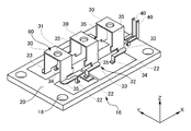
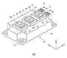
- FIG. 1 is a perspective view showing an outline of a semiconductor device 100 according to a first embodiment of the present invention.
- 2 is a perspective view showing an outline of a bottom portion 16 of a case portion 10 and a main terminal 60.
- FIG. 4 is a perspective view showing an outline of a lid part 24.
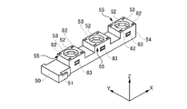
- FIG. 3 is a perspective view showing an outline of an insertion portion 50.
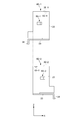
- FIG. FIG. 6 is an enlarged side view of a main terminal 60 and an end face facing portion 27. It is a schematic diagram which shows the position in the ZY surface of the end surface opposing part 27 and the end surface 61.
- FIG. 3 is an enlarged side view of a main surface opposing portion 55 and a main surface portion 30 of a main terminal 60.
- FIG. It is a schematic diagram which shows the cross section of the insertion part 50 and the main terminal 60 in a YZ surface. It is a figure which shows the shape in the XY plane and XZ plane of the side protrusion part 83.
- FIG. It is a figure which shows the main terminal 60 and the press part 26 in a YZ surface. It is a figure explaining the position of the side protrusion part 83.
- FIG. It is a figure which shows an example of the structure of the side part. It is a figure which shows the modification of the position which provides the side protrusion part 83.
- FIG. It is a perspective view which shows the outline
- FIG. 4 is a perspective view showing an outline of a main terminal 60 in the semiconductor device 200.
- FIG. 5 is a side view showing an example of a shape of an end surface protrusion 81.
- FIG. 2 is a diagram illustrating an example of a circuit 300 including an electronic circuit housed in a semiconductor device 100.
- FIG. 1 is a perspective view showing an outline of a semiconductor device 100 according to the first embodiment of the present invention.
- the semiconductor device 100 accommodates an electronic circuit such as a semiconductor chip inside.
- the semiconductor device 100 of this example includes a case unit 10, a plurality of main terminals 60, and a plurality of control terminals 40.
- the main terminal 60 is an example of a terminal portion.
- the case unit 10 accommodates an electronic circuit such as a semiconductor chip inside.
- the case portion 10 includes a bottom portion having a substrate on which an electronic circuit is placed, a lid portion 24, and an insertion portion 50.
- the lid portion 24 is fixed to the bottom portion by adhesion or the like and covers at least a part of the bottom portion.
- An electronic circuit is placed on the bottom covered with the lid 24.
- the lid 24 is made of an insulating material such as resin.
- a through hole 14 such as a screw hole for fixing the semiconductor device 100 to the outside is provided at a corner of the lid 24.
- a plane parallel to the front surface of the case portion 10 is defined as an XY plane.
- the longitudinal direction of the front surface of the case part 10 be an X direction
- a transversal direction be a Y direction.
- the lateral direction may be the X direction
- the longitudinal direction may be the Y direction.
- a direction perpendicular to the XY plane is taken as a Z direction.
- the Z direction may be referred to as the height direction.
- the direction from the bottom of the case portion 10 toward the front surface of the lid portion 24 may be referred to as “up”, and the direction from the front surface of the lid portion 24 toward the bottom portion may be referred to as “down”.
- the vertical direction does not necessarily match the gravity direction.
- the side with an arrow is the plus side and the opposite side is the minus side.
- the main terminal 60 is electrically connected to an electronic circuit covered with the lid 24.
- the main terminal 60 is formed of a conductive material.
- each main terminal 60 becomes a current path of a large current flowing in a power device such as an IGBT.
- At least a part of the main surface portion 30 of the main terminal 60 is exposed on the front surface of the case portion 10.
- the main terminal 60 of this example has a plate shape.
- the main surface portion 30 of the main terminal 60 is exposed on the front surface of the lid portion 24 and has a surface substantially parallel to the front surface.
- a through hole 31 is formed in the main surface portion 30 of the main terminal 60.
- the semiconductor device 100 is fixed to an external bus bar or the like by inserting screws or the like into the through holes 31.
- the main terminal 60 further has a side surface portion extending from the main surface portion 30 toward the bottom portion of the case portion 10.
- the side surface portion is electrically connected to an electronic circuit provided at the bottom of the case portion 10.
- the lid 24 is provided with an opening for exposing a part of the main terminal 60.
- the opening is a slit extending in the X direction on the front surface of the lid portion 24 and exposes the main surface portion 30 of the main terminal 60.
- the opening is provided in the center of the front surface of the lid 24 in the Y direction.
- the insertion portion 50 is provided so as to be inserted into the opening and to face the main surface portion 30 of the main terminal 60.
- the insertion portion 50 is disposed below the main surface portion 30.
- a recess is provided at a position facing the through hole 31 of the main surface portion 30.
- the lid portion 24 has the main terminal arrangement portion 12 on the front surface.
- the main terminal arrangement portion 12 is provided so as to protrude upward on the front surface of the lid portion 24.
- the main surface portion 30 of the main terminal 60 is exposed on the front surface of the main terminal arrangement portion 12.
- the main terminal placement portion 12 is also provided with an opening for inserting the insertion portion 50.
- the control terminal 40 has a linear shape with a width smaller than that of the main terminal 60. One end of the control terminal 40 is exposed on the front surface of the lid 24. The other end of the control terminal 40 is electrically connected to an electronic circuit placed on the bottom of the case unit 10.
- the lid portion 24 has a control terminal arrangement portion 13 that surrounds the control terminals 40 except for the tip.
- FIG. 2 is a perspective view showing an outline of the bottom portion 16 of the case portion 10 and the main terminal 60.
- the bottom 16 has a substrate 20 and an electronic circuit 22.
- substrate 20 has metal plates, such as a copper plate, and the insulating layer which covers the front surface of a metal plate. A metal layer may be further provided on the metal plate side of the insulating layer.
- the electronic circuit 22 is provided on the insulating layer. The electronic circuit 22 may have a pad connected to the main terminal 60 and the control terminal 40.
- a through hole 18 for fixing the semiconductor device 100 to the outside is provided at a corner portion of the substrate 20.
- the through hole 18 may be disposed so as to be substantially coaxial with the through hole 14 of the case portion 10.
- the semiconductor device 100 may include a plurality of main terminals 60.
- three main terminals 60 are arranged along the insertion direction of the insertion portion 50 (X direction in this example).
- Each main terminal 60 has a main surface portion 30, a side surface portion 35, and a foot portion 32.
- the main surface portion 30 is disposed in parallel with the XY plane.
- the side surface portion 35 is provided extending from both ends of the main surface portion 30 in the Y direction toward the bottom portion 16. Each side part 35 is arrange
- the foot portion 32 is connected to an end side of the side surface portion 35 on the bottom portion 16 side and is connected to the bottom portion 16.
- the foot 32 has elasticity so that the main terminal 60 can be tilted according to the applied force.
- the foot 32 supports the main terminal 60 so that it can be tilted in the XZ plane.
- the foot 32 may support the main terminal 60 so that it can be further tilted in the YZ plane.
- the foot part 32 of this example has an extending part 33 and a fixing part 34.
- the extending portion 33 is connected to a part of the end of the side surface portion 35 on the bottom 16 side, and is provided extending along the X direction.
- the extending portion 33 is provided on the outer side of each side surface portion 35 and extends from one end in the X direction of the end side of the side surface portion 35 on the bottom 16 side toward the other end in the X direction of the end side.
- the extending portion 33 has a plate shape parallel to the XY plane.
- the fixing portion 34 is provided at an end portion of the extending portion 33 on the side opposite to the end portion connected to the side surface portion 35.
- the fixing portion 34 is provided to extend from the end portion of the extending portion 33 toward the bottom portion 16.
- the lower end of the fixing portion 34 is fixed to the electronic circuit 22 with solder or the like.
- the main terminal 60 can be tilted in the XZ plane according to the applied force.
- the insertion part 50 is inserted into a space between two opposing side face parts 35.
- a foot portion 32 may be provided on each side surface portion 35.
- FIG. 3 is a perspective view showing an outline of the lid 24.
- the lid portion 24 has an opening 25 on the front surface in addition to the configuration shown in FIG.
- the opening 25 is formed by extending from one end in the X direction of the front surface of the lid portion 24 toward the other end.
- the main terminal arrangement portion 12 is provided on the front surface of the lid portion 24 on both sides of the opening 25 in the Y direction.
- the main terminal arrangement portion 12 is provided at a position corresponding to each main terminal 60.
- the main terminal 60 is exposed at the opening of the corresponding main terminal arrangement portion 12.
- the lid portion 24 is assembled so as to cover the bottom portion 16 from the upper side in the Z direction. At this time, each main terminal 60 is inserted into the opening along the side wall of the opening of the main terminal disposition portion 12.
- the control terminal 40 is also inserted into the opening along the side wall of the opening of the control terminal arrangement portion 13.
- Each main terminal arrangement part 12 has a ceiling part parallel to the XY plane.
- the lid portion 24 has a pressing portion 26 that extends from the ceiling portion toward the bottom portion 16.
- the pressing portion 26 is disposed along the side surface portion 35 of the main terminal 60 when the main terminal 60 is inserted into the opening of the main terminal arrangement portion 12.
- the pressing portion 26 may be disposed at the center of the side surface portion 35 in the X direction.
- the lower end of the pressing portion 26 comes into contact with the front surface of the extending portion 33 in the foot portion 32 of the main terminal 60. Thereby, the extending portion 33 can be pressed against the substrate 20 side of the bottom portion 16 to define the vertical position of the extending portion 33.
- a connecting portion 28 is provided between the main terminal arrangement portions 12 adjacent in the X direction.
- the connecting portion 28 has a thickness in the Z direction larger than the thickness of the ceiling portion of the main terminal arrangement portion 12.
- the connecting portion 28 has an end surface facing portion 27 exposed at the opening 25.
- the end surface facing portion 27 has a surface facing the end surface of the main terminal 60.
- the end surface of the main terminal 60 refers to a surface along the thickness direction of the plate-shaped terminal.
- the end surface facing portion 27 shown in FIG. 3 faces the end surface of the side surface portion 35 of the main terminal 60.
- the end surface facing portion 27 and the end surface of the main terminal 60 are parallel to the YZ plane.
- the end surface facing portion 27 has a longitudinal length in the Z direction.
- a terminal portion 29 is provided in place of the connecting portion 28 in the main terminal arrangement portion 12 arranged on the innermost side in the X direction. Similarly to the connecting portion 28, the end portion 29 also has an end face facing portion 27 exposed to the opening 25.
- Each end surface facing portion 27 is provided with an end surface protrusion 81.
- the end surface protrusion 81 has a predetermined thickness in the X direction.
- the end surface protrusion 81 may be formed integrally with the lid 24 using the same material as the lid 24.
- FIG. 4 is a perspective view showing an outline of the insertion portion 50.
- the insertion portion 50 has the same width in the Y direction and the same length in the X direction as the opening 25 provided on the front surface of the lid portion 24.
- the insertion part 50 is inserted into the opening 25 along the X direction.
- the insertion portion 50 is inserted between the main surface portion 30 of the main terminal 60 and the bottom portion 16.
- the insertion portion 50 has a main surface facing portion 55 that faces the main surface portion 30 of each main terminal 60. Each main surface facing portion 55 projects in the Z direction on the front surface of the insertion portion 50.
- the front surface 53 of each main surface facing portion 55 is provided with a recess 52 and a plurality of main surface protrusions 82.
- the recess 52 is provided at a position facing the through hole 31 of the main terminal 60.
- the recess 52 is provided in the center of the front surface 53 of the main surface facing portion 55.
- the recess 52 may have a larger diameter than the through hole 31.
- a nut or the like is disposed inside the recess 52.
- a screw or the like that has passed through the through hole 31 is fastened to a nut or the like inside the recess 52.
- the main surface portion 30 of the main terminal 60 is pressed against the main surface facing portion 55 by fastening screws or the like.
- the main surface protrusion 82 presses the main surface 30 from below.
- the main surface protrusion 82 is provided around the recess 52 on the front surface 53. At least three main surface protrusions 82 may be provided for each main terminal 60. Main surface protrusion 82 has a thickness in the Z direction.
- the main surface protrusion portion 82 may be formed integrally with the insertion portion 50 using the same material as the insertion portion 50.
- a plurality of main surface protrusions 82 may be provided on the front surface 53 of the main surface facing portion 55. When the front surface 53 of the main surface facing portion 55 is polygonal, a main surface protrusion 82 may be provided between each corner of the front surface 53 and the recess 52.
- the insertion portion 50 has a side protrusion 83 corresponding to at least one main terminal 60.
- side protrusions 83 are provided for all the main terminals 60.
- a side protrusion 83 is provided for each side portion 35.
- the side protrusion 83 has a thickness in the Y direction.
- the side protrusion 83 may be formed integrally with the insertion portion 50 using the same material as the insertion portion 50.
- the side protrusion 83 is provided at a position facing the side surface 35 of the main terminal 60 on the side wall 54 of the insertion portion 50 parallel to the XZ plane.
- the side protrusions 83 may be provided on the two side walls 54 on both sides of the insertion portion 50.
- the side surface portion 35 of the main terminal 60 is sandwiched between the side surface protruding portion 83 and the inner wall of the pressing portion 26 shown in FIG.
- the width of the side protrusion 83 in the X direction is larger than the width of the pressing portion 26 in the X direction.
- the width of the side protrusion 83 is at least twice the width of the pressing portion 26.
- the insertion part 50 may have a lock part 51 that fixes the insertion part 50 to the lid part 24 by fitting with the lid part 24.
- the lock portion 51 may be provided at an end portion of the insertion portion 50 on the side to be finally inserted into the opening 25.
- the lock part 51 of this example protrudes in the Y direction.
- the lock part 51 is fitted into a recess provided in the lid part 24.
- the insertion portion 50 may be fixed to the lid portion 24 with an adhesive or the like while being inserted into the opening 25.
- FIG. 5 is an enlarged side view of the main terminal 60 and the end face facing portion 27.
- FIG. 5 shows the XZ plane.
- the end surface protrusion 81 is provided on the end surface facing portion 27 that faces the end surface 61 of the main terminal 60.
- the end surface facing portion 27 has a surface that faces the opposite side to the insertion direction of the insertion portion 50 (that is, the X-axis minus direction) among the surfaces parallel to the YZ plane. That is, the end surface facing portion 27 and the end surface 61 of the main terminal 60 face each other in the insertion direction of the insertion portion 50.
- the end surface 61 of the main terminal 60 and the end surface projection 81 are shown separated from each other, but after the lid portion 24 is fixed to the bottom portion 16, the end surface 61 and the end surface projection 81 contact each other. .
- the end surface protrusion 81 has a tapered portion 84 whose thickness gradually increases as the distance from the bottom portion 16 increases.
- the taper portion 84 is formed at the end of the end surface protrusion 81 on the bottom 16 side. Thereby, when the cover part 24 is covered from above the bottom part 16, the main terminal 60 can be smoothly inserted into the opening 25 along the tapered part 84.
- a region other than the tapered portion 84 in the end surface protrusion 81 may have a constant thickness. That is, the end surface protrusion 81 has a surface parallel to the YZ surface.
- the end surface protrusion 81 may be formed above the center of the side surface portion 35 of the main terminal 60 in the Z direction.
- the end surface protrusion 81 may be formed at a position facing the upper end of the side surface portion 35.
- the main terminal 60 in this example is fixed to the bottom 16 at the tip 36 of the fixing portion 34. Since the extending portion 33 and the like have elasticity, the upper end of the main terminal 60 moves most in the X direction. By disposing the end surface protrusion 81 so as to face the upper half side of the main terminal 60, the position of the main terminal 60 in the X direction can be accurately defined.
- the end surface protrusion 81 may be provided on the end surface 61 of the main terminal 60.
- the end surface protrusion 81 may be provided on at least one of the end surface 61 and the end surface facing portion 27.
- the two end surface protrusions 81 may be provided so as to face each other.
- the end surface protrusion 81 provided on the end surface facing portion 27 may have a larger width in the Z direction than the end surface protrusion 81 provided on the end surface 61.
- FIG. 6 is a schematic diagram showing the positions of the end face facing portion 27 and the end face 61 on the ZY plane.
- FIG. 6 schematically shows the end face facing portion 27 and the like, and the relative sizes of the end face facing portion 27 and the like shown in FIGS. Moreover, in FIG. 6, the external shape of the end surface 61 is shown with the broken line.
- the end surface protrusion 81 is provided so as to overlap the end surface 61 of the side surface portion 35 of the main terminal 60 on the YZ plane.
- the end surface protrusion 81 has a width in the Y direction larger than the end surface 61.
- the end surface protrusion 81 has a width that is at least twice that of the end surface 61 in the Y direction.
- FIG. 7 is an enlarged side view of the main surface facing portion 55 and the main surface portion 30 of the main terminal 60.
- FIG. 7 shows the XZ plane. However, in FIG. 7, the side surface portion 35 of the main terminal 60 is omitted.
- the main surface protrusion portion 82 is provided on the front surface 53 of the main surface facing portion 55 that faces the main surface portion 30 of the main terminal 60.
- the main surface protrusion 82 may have a uniform thickness in the Z direction.
- the main surface portion 30 of the main terminal 60 and the main surface protrusion portion 82 are shown apart from each other, but after inserting and tightening screws or the like into the recess 52 and the through hole 31, the main surface portion 30. And the main surface protrusion 82 are in contact with each other.
- the main surface protruding portion 82 is provided on the main surface facing portion 55, but the main surface protruding portion 82 may be provided on the lower surface of the main surface portion 30 of the main terminal 60.
- the main surface protrusion portion 82 may be provided on at least one of the main surface portion 30 and the main surface facing portion 55.
- the two main surface protrusions 82 may be provided so as to face each other.
- the main surface protrusion 82 provided on the main surface facing portion 55 may be larger than the main surface protrusion 82 provided on the main surface 30.
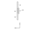
- FIG. 8 is a schematic diagram showing a cross section of the insertion portion 50 and the main terminal 60 on the YZ plane.
- the through hole 31 and the recess 52 are omitted.
- the central portion of the main surface portion 30 is pressed toward the front surface 53 side of the insertion portion 50 by a screw or the like.
- the edge of the main surface portion 30 is pressed upward by the plurality of main surface protrusions 82. Thereby, the position in the Z direction of the main surface part 30 can be specified with high accuracy.
- the side surface portion 35 of the main terminal 60 is connected to the main surface portion 30.
- the side surface portion 35 is sandwiched between the side wall 54 of the insertion portion 50 and the inner wall of the lid portion 24 (in the example shown in FIG. 3, the pressing portion 26).
- the side surface portion 35 is pressed against the inner wall of the lid portion 24 by the side surface protruding portion 83. Thereby, the position in the Y direction of the side part 35 can be prescribed
- Each main terminal 60 is pressed in the insertion direction of the insertion portion 50 (in this example, the positive direction of the X axis) in accordance with the insertion of the insertion portion 50 due to friction with the side protrusions 83. That is, as shown in FIG. 5, the end surface 61 of the main terminal 60 is pressed toward the end surface facing portion 27 side. For this reason, even if the position of the main terminal 60 in the X direction varies, by inserting the insertion portion 50, the main terminal 60 is pressed against the end surface protrusion 81 and moves to a predetermined position.
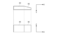
- FIG. 9 is a diagram showing the shape of the side protrusion 83 on the XY plane and the XZ plane.
- the side protrusion 83 has a tapered portion 85 whose thickness in the Y direction gradually increases as the distance from the end surface facing portion 27 of the lid 24 increases in the insertion direction of the insertion portion 50.
- the thickness of the region other than the tapered portion 85 of the side protrusion 83 may be constant.
- the taper part 85 is on the end face facing part 27 side of the side protrusion 83 (in this example, the X axis plus direction side, that is, the back side in the insertion direction of the insertion part 50). Provided at the end.
- main surface protrusion part 82 may also have a taper part similarly.
- the tapered portion is provided at the end of the main surface protrusion 82 on the end surface facing portion 27 side.
- FIG. 10 is a diagram showing the main terminal 60 and the pressing portion 26 on the YZ plane.
- the pressing portion 26 is provided by extending downward from the ceiling portion of the lid portion 24. The lower end of the pressing portion 26 abuts on the extending portion 33 of the main terminal 60.
- the pressing part 26 presses the foot part 32 of the main terminal 60 in a direction approaching the bottom part 16. Further, the main surface protrusion 82 presses the end of the main surface 30 of the main terminal 60 in a direction away from the bottom 16. For this reason, as for the side part 35, the leg part 32 side is pulled below, and the main surface part 30 side is pulled upwards. In this state, the side protrusion 83 presses the side surface 35 against the end surface of the pressing portion 26. Thereby, the position in the Z direction and Y direction of the side part 35 can be prescribed
- FIG. 11 is a diagram for explaining the position of the side protrusion 83.
- FIG. 11 shows the side surface portion 35 of the main terminal 60 in the XZ plane.
- two main surface protrusions 82 that are close to the side surface portion 35 are provided to face the main surface portion 30 of the main terminal 60.
- the insertion portion 50 is omitted, and the main surface protruding portion 82 is shown overlapping the side surface portion 35.
- the two main surface protrusions 82 adjacent to the side surface portion 35 are the two main surface protrusions closest to the side surface portion 35 among the plurality of main surface protrusion portions 82 provided to face the main surface portion 30.
- the part 82 is indicated.
- the side protrusion 83 is surrounded by two main surface protrusions 82 provided close to the side 35 and a connection point between the pressing part 26 and the extending part 33 in the XZ plane parallel to the side 35. Arranged inside the triangle 90. Two vertices of the triangle 90 corresponding to the two main surface protrusions 82 are the centers of the main surface protrusions 82 in the XZ plane.
- the side protrusion 83 may be arranged inside the triangle 90 at the center in the XZ plane. A part of the side protrusion 83 may be disposed outside the triangle 90. For example, all the regions having a constant thickness in the Y direction may be arranged inside the triangle 90, and a part of the tapered portion 85 may be arranged outside the triangle 90. Further, the entire side protrusion 83 may be disposed inside the triangle 90.
- the region surrounded by the triangle 90 is pulled up and down by the pressing portion 26 and the two main surface protrusions 82. For this reason, the distortion of the side surface portion 35 in the region is reduced.
- the position of the side surface 35 in the Y direction can be more accurately defined.
- FIG. 12 is a diagram illustrating an example of the structure of the side surface portion 35.
- FIG. 12 shows the side surface portion 35 of the main terminal 60 arranged on the most front side in the insertion direction (that is, the most minus side in the X direction).
- the side surface portion 35 has a side surface groove portion 92 at a position facing the side surface protruding portion 83.
- the side groove 92 has substantially the same shape as the side protrusion 83. However, the depth of the side groove 92 is smaller than the thickness of the side protrusion 83.
- the side protrusion 83 is fitted into the side groove 92 with the insertion portion 50 inserted into the opening 25. Thereby, it can prevent that the insertion part 50 falls out of the opening 25.
- FIG. When the side protrusion 83 is provided on the side part 35, the side groove 92 is provided on the side wall 54 of the insertion part 50.
- FIG. 13 is a diagram showing a modification of the position where the side protrusion 83 is provided.
- the insertion portion 50 is omitted, and the side surface protrusion 83 and the main surface protrusion 82 provided on the insertion portion 50 are shown superimposed on the side surface 35.
- At least one main terminal 60 may be provided with the direction in the X direction reversed from the other main terminals 60.
- at least one main terminal 60-1 is provided with the fixing portion 34 at the end of the extending portion 33 on the front side in the insertion direction (minus side in the X direction).
- at least one main terminal 60-2 is provided with a fixing portion 34 at an end portion of the extending portion 33 on the back side in the insertion direction (X direction plus side).
- the main terminal 60 rotates around the fixed portion 34 in accordance with the pressing force from the main surface protrusion 82.
- the position of the main surface protrusion 82 on the main surface 30 may be varied according to the position of the fixing portion 34.
- the main surface protrusion 82 may be provided on the side farther from the fixing portion 34 than the center of the main surface 30 in the X direction.
- the main surface protrusion 82 is not provided on the fixed portion 34 side of the main surface portion 30 in the X direction. That is, for the main terminal 60 in which the fixing portion 34 is provided on the back side in the insertion direction, the main surface protrusion 82 is provided on the near side in the insertion direction.
- a main surface protrusion 82 is provided on the back side in the insertion direction.
- the main surface protrusion 82 By providing the main surface protrusion 82 at a position away from the fixed portion 34, it is possible to define the position of the main terminal 60 that moves the most. For this reason, the position of the main terminal 60 can be defined with high accuracy.
- the main surface protrusion portion 82 may be provided only on the fixing portion 34 side from the center of the main surface portion 30 in the X direction. In this case, the position of the main terminal 60 can be defined by the main surface protrusion 82 having a small thickness.
- the position of the side protrusion 83 on the side surface 35 may be different depending on the position of the fixing portion 34.
- the side protrusion 83 may be provided closer to the fixed part 34 than the center of the side part 35 in the X direction, or may be provided on the side away from the fixed part 34.
- the main terminal 60 can be pressed against the case portion 10 in the X, Y, and Z directions, and the position of the main terminal 60 can be defined with high accuracy. Further, even when an external force is applied to the main terminal 60, the position of the main terminal 60 can be maintained. For this reason, the force applied to the bottom part 16 from the main terminal 60 can be reduced, and the intensity
- the semiconductor device 100 includes the end surface protrusion 81, the main surface protrusion 82, and the side surface protrusion 83. In another example, the semiconductor device 100 includes the end surface protrusion 81, the main surface protrusion 82, and the side surface protrusion 83. Any one or two of these may be provided.
- FIG. 14 is a perspective view showing an outline of the semiconductor device 200 according to the second embodiment.
- the semiconductor device 200 is different from the configuration of the semiconductor device 100 in that the opening 25 and the insertion portion 50 are not provided. Other configurations may be the same as those of the semiconductor device 100.
- FIG. 15 is a perspective view showing an outline of the main terminal 60 in the semiconductor device 200.
- the main terminal 60 of this example is fixed to the bottom 16 by one foot. Moreover, the main terminal 60 has one side part.
- the main surface portion 30 is provided extending from the side surface portion.
- the main terminal arrangement portion 12 is provided with a slit 97 through which the main terminal 60 passes.
- the side surface portion and the main surface portion 30 are formed on the same plane, and the main surface portion 30 is exposed above the slit 97.
- the main terminal 60 passes through the slit 97 by covering the lid portion 24 with the bottom portion 16.
- the main surface portion 30 exposed above the slit 97 is bent toward the main terminal arrangement portion 12 so that the main terminal arrangement portion 12 and the main surface portion 30 are opposed to each other.
- an end surface facing portion 94 is provided on the front surface of the main terminal arrangement portion 12 at a position facing the end surface 95 of the bent main surface portion 30.
- An end surface protrusion 81 is provided on at least one of the end surface facing portion 94 and the end surface 95. Even with such a structure, the position of the main terminal 60 can be accurately defined.
- FIG. 16 is a side view showing an example of the shape of the end surface protrusion 81.
- the end surface protrusion 81 has a tapered portion 84 at the upper end.
- the taper portion 84 has a thickness that decreases toward the upper side. Thereby, the main surface part 30 can be bent and the end surface protrusion part 81 and the end surface 95 of the main surface part 30 can be made to contact easily.
- FIG. 17 is a diagram illustrating an example of a circuit 300 including an electronic circuit housed in the semiconductor device 100.
- the circuit 300 of this example is a three-phase inverter circuit provided between the power supply 210 and the load 220.
- the load 220 is, for example, a three-phase motor.
- the circuit 300 converts the power supplied from the power source 210 into a three-phase signal (AC voltage) and supplies the signal to the load 220.
- AC voltage three-phase signal
- the circuit 300 has three bridges corresponding to three-phase signals.
- Each bridge has an upper arm 152 and a lower arm 154 provided in series between a positive wiring and a negative wiring.
- Each arm is provided with a transistor 202 such as an IGBT and a diode 204 such as an FWD.
- a signal of each phase is output from a connection point between the upper arm 152 and the lower arm 154.
- the circuit 300 includes two sense units 208.
- One sense unit 208 detects a current at a connection point between the upper arm 152 and the lower arm 154.
- the other sense unit 208 detects a current at a connection point between the lower arm 154 and the reference potential.
- the upper arm 152, the lower arm 154, and the sense unit 208 in one bridge are accommodated in one semiconductor device 100.
- Three main terminals 60 may be connected to the power source 210 and the load 220, respectively.
- a pair of control terminals 40 may be connected to the sense unit 208 and the gate driving unit, respectively.
- one arm may be accommodated in one semiconductor device 100, and the entire circuit 300 may be accommodated in one semiconductor device 100.
Landscapes
- Photovoltaic Devices (AREA)
- Connecting Device With Holders (AREA)
Abstract
【課題】半導体装置における主端子の位置を精度よく規定する。 【解決手段】主面部に貫通孔を有する端子部と、貫通孔と対向する位置に窪みを有するケース部とを備え、ケース部は、端子部の端面と対向する端面対向部を有し、端面と端面対向部の少なくとも一方に端面突起部を設けた半導体装置を提供する。
Description
本発明は、半導体装置に関する。
従来、半導体チップ等を収容する半導体装置において、外部のバスバー等に固定される主端子を備える構造が知られている(例えば、特許文献1参照)。主端子は、樹脂ケースの表面において所定の位置に配置される。
特許文献1 実開平5-15445号公報
特許文献1 実開平5-15445号公報
半導体装置の組み立てを容易にするために、樹脂ケースと主端子との間には、クリアランスが設けられる。このため、半導体装置の組み立て時等において、樹脂ケースに対する主端子の相対的な位置にはバラツキが生じてしまう。
本発明の第1の態様においては、主面部に貫通孔を有する端子部と、貫通孔と対向する位置に窪みを有するケース部とを備える半導体装置を提供する。ケース部は、端子部の端面と対向する端面対向部を有してよい。端面と端面対向部の少なくとも一方に端面突起部を設けてよい。
ケース部は、半導体チップが載置され、端子部が固定される底部を有してよい。ケース部は、底部の少なくとも一部を覆い、且つ、端子部の主面部を露出させる開口が設けられた蓋部を有してよい。ケース部は、蓋部の開口において、端子部の主面部と底部との間に挿入され、端子部の貫通孔と対向する位置に窪みを有する挿入部を有してよい。挿入部の挿入方向において、端子部の端面と対向する蓋部に端面対向部が設けられてよい。端面突起部は、底部から離れるほど徐々に厚みが増加するテーパー部を有してよい。
挿入部は、端子部の主面部と対向する主面対向部を有してよい。主面部と主面対向部の少なくとも一方に主面突起部を設けてよい。主面突起部を、端子部毎に少なくとも3つ設けてよい。
端子部は、主面部と連結され、挿入部の側壁および蓋部の内壁に挟まれる側面部を有してよい。端子部の側面部と、挿入部の側壁の少なくとも一方に側面突起部を設けてよい。側面突起部は、挿入方向において、蓋部の端面対向部から離れるほど徐々に厚みが増加するテーパー部を有してよい。
端子部は、側面部と連結され、且つ、ケース部の底部に固定される足部を更に備えてよい。ケース部は、足部をケース部の底部に向けて押圧する押圧部を有してよい。主面突起部は、挿入部の主面対向部に設けられ、端子部の主面部をケース部の底部から離れる方向に押圧してよい。
側面突起部は、端子部の側面部と平行な面内において、側面部と近接して設けられた2つの主面突起部と、押圧部および足部の接続点とで囲まれる三角形の内部に配置されてよい。
挿入方向に沿って複数の端子部が配列されてよい。それぞれの端子部に対応して、側面突起部が設けられてよい。挿入方向において最も手前に設けられた端子部に対応して、端子部の側面部と、挿入部の側壁の一方に、側面突起部と嵌合する側面溝部が設けられていてよい。
足部は、挿入方向に延伸する延伸部と、延伸部の挿入方向におけるいずれかの端部から、ケース部の底部に向かって延伸して設けられ、底部に固定される固定部とを有してよい。少なくとも一つの端子部は、端面突起部に近い側の延伸部の端部に固定部が設けられてよい。少なくとも一つの端子部は、端面突起部から遠い側の延伸部の端部に固定部が設けられてよい。それぞれの端子部において、固定部の位置に応じて主面突起部の位置が異なっていてよい。
なお、上記の発明の概要は、本発明の特徴の全てを列挙したものではない。また、これらの特徴群のサブコンビネーションもまた、発明となりうる。
以下、発明の実施の形態を通じて本発明を説明するが、以下の実施形態は請求の範囲にかかる発明を限定するものではない。また、実施形態の中で説明されている特徴の組み合わせの全てが発明の解決手段に必須であるとは限らない。
図1は、本発明の第1の実施形態に係る半導体装置100の概要を示す斜視図である。半導体装置100は、半導体チップ等の電子回路を内部に収容する。本例の半導体装置100は、ケース部10、複数の主端子60および複数の制御端子40を備える。主端子60は、端子部の一例である。
ケース部10は、半導体チップ等の電子回路を内部に収容する。一例としてケース部10は、電子回路が載置される基板を有する底部と、蓋部24と、挿入部50とを有する。蓋部24は、接着等により底部に固定され、底部の少なくとも一部を覆う。蓋部24により覆われる底部には、電子回路が載置される。蓋部24は、樹脂等の絶縁材料で形成される。蓋部24の角部には、外部に半導体装置100を固定するためのねじ穴等の貫通孔14が設けられる。
なお、本明細書においてはケース部10のおもて面と平行な面をXY面とする。また、ケース部10のおもて面の長手方向をX方向、短手方向をY方向とする。ただし、短手方向がX方向であり、長手方向がY方向であってもよい。また、XY面と垂直な方向をZ方向とする。本明細書では、Z方向を高さ方向と称する場合がある。また、ケース部10の底部から、蓋部24のおもて面に向かう方向を上、蓋部24のおもて面から底部に向かう方向を下と称する場合がある。ただし上下の方向は重力方向とは必ずしも一致しない。また、各図に示したXYZ座標軸において、矢印を付した側をプラス側、逆側をマイナス側とする。
主端子60は、蓋部24に覆われた電子回路と電気的に接続される。主端子60は、導電材料で形成される。例えばそれぞれの主端子60は、IGBT等のパワーデバイスに流れる大電流の電流経路となる。主端子60の主面部30の少なくとも一部は、ケース部10のおもて面に露出する。本例の主端子60は、板形状を有する。
主端子60の主面部30は、蓋部24のおもて面において露出しており、且つ、当該おもて面とほぼ平行な面を有する。主端子60の主面部30には、貫通孔31が形成される。貫通孔31にねじ等が挿入されることで、半導体装置100は、外部のバスバー等に固定される。
主端子60は、主面部30からケース部10の底部に向かって延伸する側面部を更に有する。当該側面部は、ケース部10の底部に設けられた電子回路と電気的に接続される。
蓋部24には、主端子60の一部を露出させるための開口が設けられる。本例において当該開口は、蓋部24のおもて面においてX方向に延伸するスリットであり、主端子60の主面部30を露出させる。当該開口は、蓋部24のおもて面の、Y方向における中央に設けられる。
挿入部50は、当該開口に挿入されて、主端子60の主面部30と対向するように設けられる。本例において挿入部50は、主面部30の下側に配置される。挿入部50において、主面部30の貫通孔31と対向する位置には窪みが設けられる。当該窪みにナット等を設けることで、貫通孔31を通過したねじ等を当該窪みに締結できる。
蓋部24は、おもて面において主端子配置部12を有する。主端子配置部12は、蓋部24のおもて面において、上方向に突出して設けられる。主端子60の主面部30は、主端子配置部12のおもて面に露出する。ただし、主端子配置部12にも、挿入部50を挿入するための開口が設けられる。
制御端子40は、主端子60よりも幅の小さい線形状を有する。制御端子40の一つの端部は、蓋部24のおもて面において露出する。制御端子40の他方の端部は、ケース部10の底部に載置された電子回路に電気的に接続される。蓋部24は、制御端子40の先端以外を囲む制御端子配置部13を有する。
図2は、ケース部10の底部16と、主端子60の概要を示す斜視図である。底部16は、基板20および電子回路22を有する。基板20は、銅板等の金属板と、金属板のおもて面を覆う絶縁層とを有する。絶縁層の金属板側にさらに金属層を有してもよい。電子回路22は、当該絶縁層上に設けられる。電子回路22は、主端子60および制御端子40と接続するパッドを有してよい。基板20の角部には、半導体装置100を外部に固定するための貫通孔18が設けられる。貫通孔18はケース部10の貫通孔14と略同軸となるよう配置されてよい。
半導体装置100は、複数の主端子60を備えてよい。図2の例では、3個の主端子60が、挿入部50の挿入方向(本例ではX方向)に沿って配列されている。それぞれの主端子60は、主面部30、側面部35および足部32を有する。主面部30は、XY面と平行に配置される。
側面部35は、主面部30のY方向における両端から、底部16に向かって延伸して設けられる。それぞれの側面部35は、XZ面と平行に配置される。足部32は、側面部35の底部16側の端辺に連結され、底部16と接続される。
足部32は、印加される力に応じて主端子60を傾かせることができるように、弾性を有する。例えば足部32は、主端子60を、XZ面内で傾かせることができるように支持する。また足部32は、主端子60を、更にYZ面内で傾かせることができるように支持してもよい。
本例の足部32は、延伸部33および固定部34を有する。延伸部33は、側面部35の底部16側の端辺の一部に連結され、X方向に沿って延伸して設けられる。一例として延伸部33は、それぞれの側面部35の外側に設けられ、側面部35の底部16側の端辺のX方向における一端から、当該端辺のX方向における他端に向けて延伸する。延伸部33は、XY面と平行な板形状を有する。
固定部34は、延伸部33の端部のうち、側面部35と接続される端部とは逆側の端部に設けられる。固定部34は、延伸部33の当該端部から底部16に向かって延伸して設けられる。固定部34の下端は、半田等により電子回路22に固定される。
このような構成により、主端子60は、印加される力に応じて、XZ面内で傾くことができる。それぞれの主端子60において対向する2つの側面部35に挟まれる空間には、挿入部50が挿入される。主端子60が、挿入部50の挿入位置等のばらつきに応じて傾くことで、挿入部50を容易に挿入することができる。それぞれの側面部35に足部32が設けられてよい。
図3は、蓋部24の概要を示す斜視図である。蓋部24は、図1に示した構成に加えて、おもて面に開口25を有する。開口25は、蓋部24のおもて面のX方向の一端から、他端に向けて延伸して形成される。
蓋部24のおもて面には、開口25のY方向における両側に、主端子配置部12が設けられる。主端子配置部12は、それぞれの主端子60と対応する位置に設けられる。主端子60は、対応する主端子配置部12の開口において露出する。蓋部24は、Z方向における上側から、底部16に被せるように組み立てられる。このとき、それぞれの主端子60は、主端子配置部12の開口の側壁に沿って、当該開口に挿入される。また、制御端子40も、制御端子配置部13の開口の側壁に沿って、当該開口に挿入される。
それぞれの主端子配置部12は、XY面と平行な天井部を有する。また、蓋部24は、当該天井部から底部16に向かって延伸する押圧部26を有する。押圧部26は、主端子配置部12の開口に主端子60が挿入された場合に、主端子60の側面部35に沿うように配置される。押圧部26は、側面部35のX方向における中心に配置されてよい。
押圧部26の下端は、主端子60の足部32における延伸部33のおもて面と当接する。これにより、延伸部33を底部16の基板20側に押圧して、延伸部33の上下方向の位置を規定することができる。
また、X方向において隣接する主端子配置部12の間には、連結部28が設けられる。連結部28は、Z方向における厚みが、主端子配置部12の天井部の厚みよりも大きい。連結部28は、開口25に露出する端面対向部27を有する。端面対向部27は、主端子60の端面と対向する面を有する。本例において主端子60の端面とは、板形状の端子の厚み方向に沿った面を指す。図3に示す端面対向部27は、主端子60の側面部35における端面と対向する。本例において端面対向部27および主端子60の端面は、YZ面と平行である。端面対向部27は、Z方向に長手を有する。
なお、X方向において最も奥側に配置される主端子配置部12には、連結部28に代えて終端部29が設けられる。終端部29も、連結部28と同様に、開口25に露出する端面対向部27を有する。
それぞれの端面対向部27には、端面突起部81が設けられる。端面突起部81は、X方向において所定の厚みを有する。端面突起部81は、蓋部24と同一の材料で、蓋部24と一体に成形されてよい。端面突起部81を設けることで、端面対向部27に対する主端子60のX方向における位置を精度よく規定できる。
図4は、挿入部50の概要を示す斜視図である。挿入部50は、蓋部24のおもて面に設けた開口25と、Y方向において同一の幅を有し、X方向において同一の長さを有する。挿入部50は、X方向に沿って開口25に挿入される。挿入部50は、主端子60の主面部30と、底部16の間に挿入される。
挿入部50は、それぞれの主端子60の主面部30と対向する主面対向部55を有する。それぞれの主面対向部55は、挿入部50のおもて面において、Z方向に突出する。それぞれの主面対向部55のおもて面53には、窪み52および複数の主面突起部82が設けられる。
窪み52は、主端子60の貫通孔31と対向する位置に設けられる。一例として窪み52は、主面対向部55のおもて面53の中央に設けられる。窪み52は、貫通孔31よりも大きい直径を有してよい。窪み52の内部にはナット等が配置される。貫通孔31を通過したねじ等が、窪み52の内部のナット等に締結する。
ねじ等を締結することで、主端子60の主面部30は、主面対向部55に押し付けられる。一方で、主面突起部82は、主面部30を下方から押圧する。このような構成により、主面部30のZ方向における位置を精度よく規定できる。
主面突起部82は、おもて面53において窪み52の周囲に設けられる。主面突起部82は、主端子60毎に少なくとも3つ設けてよい。主面突起部82は、Z方向に厚みを有する。主面突起部82は、挿入部50と同一の材料で、挿入部50と一体に成形されてよい。主面対向部55のおもて面53には、複数の主面突起部82が設けられてよい。主面対向部55のおもて面53が多角形形状の場合、おもて面53のそれぞれの角と、窪み52との間に主面突起部82が設けられてよい。
また、挿入部50は、少なくとも一つの主端子60に対応して、側面突起部83を有する。図4の例では、全ての主端子60に対して側面突起部83が設けられている。また、それぞれの主端子60において、側面部35毎に側面突起部83が設けられる。側面突起部83は、Y方向に厚みを有する。側面突起部83は、挿入部50と同一の材料で、挿入部50と一体に成形されてよい。
側面突起部83は、XZ面に平行な挿入部50の側壁54において、主端子60の側面部35と対向する位置に設けられる。側面突起部83は、挿入部50の両側の2つの側壁54に設けられてよい。主端子60の側面部35は、側面突起部83および図3に示した押圧部26の内壁に挟まれる。側面突起部83を設けることで、主端子60の側面部35のY方向における位置を精度よく規定することができる。
側面突起部83のX方向における幅は、押圧部26のX方向における幅よりも大きい。例えば側面突起部83の幅は、押圧部26の幅の2倍以上である。
また、挿入部50は、蓋部24と嵌合することで、挿入部50を蓋部24に固定するロック部51を有してよい。ロック部51は、例えば挿入部50のうち、最後に開口25に挿入される側の端部に設けられてよい。本例のロック部51はY方向に突出している。ロック部51は、蓋部24に設けられる窪みと嵌合する。挿入部50は、開口25に挿入された状態で、接着剤等で蓋部24に固定されてもよい。
図5は、主端子60および端面対向部27を拡大した側面図である。図5はXZ面を示している。図3において説明したように、主端子60の端面61と対向する端面対向部27には、端面突起部81が設けられる。端面対向部27は、YZ面に平行な面のうち、挿入部50の挿入方向とは逆側(すなわち、X軸マイナス方向)を向く面を有する。つまり、端面対向部27および主端子60の端面61は、挿入部50の挿入方向において対向する。なお、図5においては主端子60の端面61と、端面突起部81とを離して示しているが、蓋部24を底部16に固定した後は、端面61と端面突起部81は接している。
端面突起部81は、底部16から離れるほど徐々に厚みが増加するテーパー部84を有する。テーパー部84は、端面突起部81の底部16側の端部に形成される。これにより、蓋部24を底部16の上方から被せる場合に、主端子60をテーパー部84に沿って開口25にスムーズに挿入できる。端面突起部81においてテーパー部84以外の領域は、厚みが一定であってよい。つまり、端面突起部81は、YZ面と平行な面を有する。
端面突起部81は、主端子60の側面部35のZ方向における中央よりも上側に形成されてよい。端面突起部81は、側面部35の上端と対向する位置に形成されてもよい。本例の主端子60は、固定部34の先端36において底部16に固定される。延伸部33等が弾性を有するので、主端子60の上端がX方向において最も大きく動く。端面突起部81を主端子60の上半分側に対向して配置することで、主端子60のX方向の位置を精度よく規定することができる。
本例では、端面対向部27に端面突起部81を設ける例を示したが、端面突起部81は、主端子60の端面61に設けてもよい。端面突起部81は、端面61および端面対向部27の少なくとも一方に設ければよい。端面61および端面対向部27の両方に端面突起部81を設ける場合、2つの端面突起部81が対向するように設けてもよい。この場合、端面対向部27に設ける端面突起部81は、端面61に設ける端面突起部81よりもZ方向の幅が大きくてよい。
図6は、端面対向部27および端面61のZY面における位置を示す模式図である。図6では、端面対向部27等を模式的に示しており、図1から図5に示した端面対向部27等とは相対的な大きさは一致していない。また、図6では端面61の外形を破線で示している。
端面突起部81は、主端子60の側面部35における端面61と、YZ面において重なるように設けられる。端面突起部81は、Y方向における幅が端面61の幅よりも大きい。例えば端面突起部81は、Y方向において端面61の2倍以上の幅を有する。これにより、端面61の位置がY方向においてずれた場合でも、端面突起部81と端面61とを接触させることができる。
図7は、主面対向部55および主端子60の主面部30を拡大した側面図である。図7はXZ面を示している。ただし図7においては、主端子60の側面部35を省略している。図4において説明したように、主端子60の主面部30と対向する主面対向部55のおもて面53には、主面突起部82が設けられる。主面突起部82は、Z方向において均一な厚みを有してよい。なお、図7においては主端子60の主面部30と、主面突起部82とを離して示しているが、窪み52および貫通孔31にねじ等を挿入して締結した後は、主面部30と主面突起部82とは接している。
本例では、主面対向部55に主面突起部82を設ける例を示したが、主面突起部82は、主端子60の主面部30の下面に設けてもよい。主面突起部82は、主面部30および主面対向部55の少なくとも一方に設ければよい。主面部30および主面対向部55の両方に主面突起部82を設ける場合、2つの主面突起部82が対向するように設けてもよい。この場合、主面対向部55に設ける主面突起部82は、主面部30に設ける主面突起部82よりも大きくてよい。
図8は、YZ面における挿入部50および主端子60の断面を示す模式図である。図8においては、貫通孔31および窪み52を省略している。主面部30の中央部分は、ねじ等により挿入部50のおもて面53側に押圧される。一方で、主面部30の縁部は、複数の主面突起部82により上側に押圧される。これにより、主面部30のZ方向における位置を精度よく規定できる。
主端子60の側面部35は、主面部30と連結される。側面部35は、挿入部50の側壁54および蓋部24の内壁(図3に示した例では、押圧部26)に挟まれる。側面部35は、側面突起部83により、蓋部24の内壁に押し付けられる。これにより、側面部35のY方向における位置を精度よく規定できる。
なお、それぞれの主端子60は、側面突起部83との摩擦により、挿入部50が挿入されるのに応じて挿入部50の挿入方向(本例ではX軸プラス方向)に押圧される。つまり、図5に示したように主端子60の端面61が、端面対向部27側に押圧される。このため、主端子60のX方向の位置にばらつきが生じていても、挿入部50を挿入することで、主端子60が端面突起部81に押し付けられて、所定の位置に移動する。
そして、挿入部50を挿入し終わっても、側面突起部83が主端子60の側面部35を蓋部24の内壁に押し付ける状態が維持される。このため、挿入部50が固定されて、主端子60が端面対向部27に押し付けられる状態が維持される。これにより、X方向における主端子60の位置を、精度よく規定することができる。
図9は、側面突起部83のXY面およびXZ面における形状を示す図である。図9に示すように、側面突起部83は、挿入部50の挿入方向において、蓋部24の端面対向部27から離れるほど徐々にY方向の厚みが増加するテーパー部85を有する。側面突起部83のテーパー部85以外の領域の厚みは一定であってよい。側面突起部83が挿入部50に設けられる場合、テーパー部85は、側面突起部83における端面対向部27側(本例ではX軸プラス方向側、すなわち挿入部50の挿入方向における奥側)の端部に設けられる。
なお、主面突起部82も、同様にテーパー部を有してもよい。挿入部50に主面突起部82が設けられる場合、当該テーパー部は、主面突起部82における端面対向部27側の端部に設けられる。
図10は、YZ面における主端子60および押圧部26を示す図である。上述したように、押圧部26は、蓋部24の天井部分から下方に延伸して設けられる。押圧部26の下端は、主端子60の延伸部33に当接する。
これにより、押圧部26は主端子60の足部32を、底部16に近づく方向に押圧する。また、主面突起部82は、主端子60の主面部30の端部を、底部16から離れる方向に押圧する。このため、側面部35は、足部32側が下方に引っ張られ、主面部30側が上方に引っ張られる。この状態で、側面突起部83が側面部35を押圧部26の端面に押し付ける。これにより、側面部35のZ方向およびY方向における位置を、精度よく規定することができる。
図11は、側面突起部83の位置を説明する図である。図11は、XZ面における主端子60の側面部35を示している。また、主端子60の主面部30と対向して、側面部35に近接する2つの主面突起部82が設けられている。図11では挿入部50を省略して、主面突起部82を側面部35に重ねて示している。ここで側面部35に近接する2つの主面突起部82とは、主面部30に対向して設けられた複数の主面突起部82のうち、当該側面部35に最も近い2つの主面突起部82を指す。
側面突起部83は、側面部35と平行なXZ面内において、側面部35と近接して設けられた2つの主面突起部82と、押圧部26および延伸部33の接続点とで囲まれる三角形90の内部に配置される。2つの主面突起部82に対応する三角形90の2つの頂点は、XZ面における主面突起部82の中心である。
側面突起部83は、XZ面における中心が三角形90の内側に配置されてよい。側面突起部83は、一部が三角形90の外側に配置されてよい。例えば、Y方向の厚みが一定の領域が全て三角形90の内部に配置され、テーパー部85の一部が三角形90の外側に配置されてよい。また、側面突起部83の全体が三角形90の内部に配置されてもよい。
三角形90で囲まれる領域は、押圧部26および2つの主面突起部82により上下方向に引っ張られる。このため、当該領域における側面部35は歪が小さくなる。当該領域に側面突起部83を設けることで、側面部35のY方向における位置をより精度よく規定できる。
図12は、側面部35の構造の一例を示す図である。図12は、挿入方向において最も手前側(すなわち、X方向において最もマイナス側)に配置された主端子60の側面部35を示している。
側面部35は、側面突起部83と対向する位置に側面溝部92を有する。側面溝部92は、側面突起部83とほぼ同一の形状を有する。ただし、側面溝部92の深さは、側面突起部83の厚みよりも小さい。
これにより、挿入部50を開口25に挿入した状態で、側面突起部83が側面溝部92に嵌合する。これにより、挿入部50が開口25から脱落することを防止できる。なお、側面突起部83が側面部35に設けられている場合、側面溝部92は、挿入部50の側壁54に設けられる。
図13は、側面突起部83を設ける位置の変形例を示す図である。図13においては、挿入部50は省略しており、挿入部50に設けられる側面突起部83および主面突起部82を側面部35に重ねて示している。
図2に示すように、少なくとも一つの主端子60は、他の主端子60とはX方向における向きが反転して設けられてよい。つまり、少なくとも一つの主端子60-1は、挿入方向手前側(X方向マイナス側)の延伸部33の端部に固定部34が設けられる。また、少なくとも一つの主端子60-2は、挿入方向奥側(X方向プラス側)の延伸部33の端部に固定部34が設けられる。
主端子60は、主面突起部82からの押圧力に応じて、固定部34を軸として回転する。本例では、主面部30における主面突起部82の位置を、固定部34の位置に応じて異ならせてよい。例えば、それぞれの主端子60において、主面部30のX方向の中央よりも、固定部34から離れる側に主面突起部82を設けてよい。主面部30のX方向の中央よりも固定部34側には、主面突起部82が設けられない。つまり、固定部34が挿入方向奥側に設けられる主端子60に対しては、主面突起部82が挿入方向手前側に設けられる。また、固定部34が挿入方向手前側に設けられる主端子60に対しては、主面突起部82が挿入方向奥側に設けられる。
主面突起部82を、固定部34から離れた位置に設けることで、主端子60のうち、最も大きく動く部分の位置を規定することができる。このため、主端子60の位置を精度よく規定することができる。
また、それぞれの主端子60において、主面部30のX方向の中央よりも、固定部34側だけに主面突起部82を設けてもよい。この場合、厚みの小さい主面突起部82で、主端子60の位置を規定することができる。
また、それぞれの主端子60において、側面部35における側面突起部83の位置が、固定部34の位置に応じて異なってよい。例えば、側面突起部83は、側面部35のX方向の中央よりも固定部34側に設けられてよく、固定部34から離れた側に設けられてもよい。
以上説明した半導体装置100によれば、X、Y、Z方向において、主端子60をケース部10に押し当てることができ、主端子60の位置を高精度に規定できる。また、主端子60に外力が印加されても、主端子60の位置を維持することができる。このため、主端子60から底部16に印加される力を低減でき、外力に対する強度を向上させることができる。例えば、主端子60の主面部30をねじ等によって主面対向部55に締結する場合に生じる圧縮および引張応力に対する強度を向上させることができる。また、半導体装置100は、端面突起部81、主面突起部82および側面突起部83を備えていたが、他の例では、端面突起部81、主面突起部82および側面突起部83のうちのいずれか1種または2種だけを備えていてもよい。
図14は、第2の実施形態に係る半導体装置200の概要を示す斜視図である。半導体装置200は、半導体装置100の構成に対して、開口25および挿入部50を備えない点で相違する。他の構成は、半導体装置100と同一であってよい。
図15は、半導体装置200における、主端子60の概要を示す斜視図である。本例の主端子60は、一つの足部によって底部16に固定される。また、主端子60は、一つの側面部を有する。主面部30は、側面部から延伸して設けられる。
主端子配置部12には、主端子60が通過するスリット97が設けられる。主端子60において側面部および主面部30は同一の平面上に形成されており、スリット97の上方に主面部30が露出する。
蓋部24を底部16に被せることで、主端子60がスリット97を通過する。スリット97の上方に露出した主面部30を、主端子配置部12に向けて折り曲げることで、主端子配置部12と主面部30とを対向させる。
また、主端子配置部12のおもて面には、折り曲げられた主面部30の端面95と対向する位置に、端面対向部94が設けられる。端面対向部94と端面95の少なくとも一方には、端面突起部81が設けられる。このような構造によっても、主端子60の位置を精度よく規定することができる。
図16は、端面突起部81の形状の一例を示す側面図である。端面突起部81は、上側の端部にテーパー部84を有する。テーパー部84は、上側ほど厚みが減少している。これにより、主面部30を折り曲げて、端面突起部81と主面部30の端面95とを容易に接触させることができる。
図17は、半導体装置100に収容された電子回路を含む回路300の例を示す図である。本例の回路300は、電源210および負荷220の間に設けられた3相インバータ回路である。負荷220は例えば3相モーターである。回路300は、電源210から供給される電力を、3相の信号(交流電圧)に変換して負荷220に供給する。
回路300は、3相の信号に対応する3つのブリッジを有する。それぞれのブリッジは、正側配線と負側配線との間に、直列に設けられた上側アーム152および下側アーム154を有する。それぞれのアームは、IGBT等のトランジスタ202と、FWD等のダイオード204が設けられる。上側アーム152および下側アーム154の接続点から、各相の信号が出力される。
また、回路300は、2つのセンス部208を有する。一方のセンス部208は、上側アーム152および下側アーム154の接続点における電流を検出する。他方のセンス部208は、下側アーム154と基準電位の接続点における電流を検出する。
本例では、一つのブリッジにおける上側アーム152、下側アーム154およびセンス部208が、一つの半導体装置100に収容される。3つの主端子60がそれぞれ電源210および負荷220に接続されてよい。一対の制御端子40がそれぞれセンス部208およびゲート駆動部に接続されてよい。他の例では、一つのアームが一つの半導体装置100に収容されてよく、回路300全体が一つの半導体装置100に収容されてもよい。
以上、本発明を実施の形態を用いて説明したが、本発明の技術的範囲は上記実施の形態に記載の範囲には限定されない。上記実施の形態に、多様な変更または改良を加えることが可能であることが当業者に明らかである。その様な変更または改良を加えた形態も本発明の技術的範囲に含まれ得ることが、請求の範囲の記載から明らかである。
請求の範囲、明細書、および図面中において示した装置、システム、プログラム、および方法における動作、手順、ステップ、および段階等の各処理の実行順序は、特段「より前に」、「先立って」等と明示しておらず、また、前の処理の出力を後の処理で用いるのでない限り、任意の順序で実現しうることに留意すべきである。請求の範囲、明細書、および図面中の動作フローに関して、便宜上「まず、」、「次に、」等を用いて説明したとしても、この順で実施することが必須であることを意味するものではない。
10・・・ケース部、12・・・主端子配置部、13・・・制御端子配置部、14・・・貫通孔、16・・・底部、18・・・貫通孔、20・・・基板、22・・・電子回路、24・・・蓋部、25・・・開口、26・・・押圧部、27・・・端面対向部、28・・・連結部、29・・・終端部、30・・・主面部、31・・・貫通孔、32・・・足部、33・・・延伸部、34・・・固定部、35・・・側面部、36・・・先端、40・・・制御端子、50・・・挿入部、51・・・ロック部、52・・・窪み、53・・・おもて面、54・・・側壁、55・・・主面対向部、60・・・主端子、61・・・端面、81・・・端面突起部、82・・・主面突起部、83・・・側面突起部、84・・・テーパー部、85・・・テーパー部、90・・・三角形、92・・・側面溝部、94・・・端面対向部、95・・・端面、97・・・スリット、100・・・半導体装置、152・・・上側アーム、154・・・下側アーム、200・・・半導体装置、202・・・トランジスタ、204・・・ダイオード、208・・・センス部、210・・・電源、220・・・負荷、300・・・回路
Claims (12)
- 主面部に貫通孔を有する端子部と、
前記貫通孔と対向する位置に窪みを有するケース部と
を備え、
前記ケース部は、前記端子部の端面と対向する端面対向部を有し、
前記端面と前記端面対向部の少なくとも一方に端面突起部を設けた
半導体装置。 - 前記ケース部は、
半導体チップが載置され、前記端子部が固定される底部と、
前記底部の少なくとも一部を覆い、且つ、前記端子部の主面部を露出させる開口が設けられた蓋部と、
前記蓋部の前記開口において、前記端子部の主面部と前記底部との間に挿入され、前記端子部の前記貫通孔と対向する位置に前記窪みを有する挿入部と
を有し、
前記挿入部の挿入方向において、前記端子部の前記端面と対向する前記蓋部に前記端面対向部が設けられる
請求項1に記載の半導体装置。 - 前記端面突起部は、前記底部から離れるほど徐々に厚みが増加するテーパー部を有する
請求項2に記載の半導体装置。 - 前記挿入部は、前記端子部の前記主面部と対向する主面対向部を有し、
前記主面部と前記主面対向部の少なくとも一方に主面突起部を設けた
請求項2に記載の半導体装置。 - 前記主面突起部を、前記端子部毎に少なくとも3つ設けた
請求項4に記載の半導体装置。 - 前記端子部は、前記主面部と連結され、前記挿入部の側壁および前記蓋部の内壁に挟まれる側面部を有し、
前記端子部の前記側面部と、前記挿入部の前記側壁の少なくとも一方に側面突起部を設けた
請求項4または5に記載の半導体装置。 - 前記側面突起部は、前記挿入方向において、前記蓋部の前記端面対向部から離れるほど徐々に厚みが増加するテーパー部を有する
請求項6に記載の半導体装置。 - 前記端子部は、前記側面部と連結され、且つ、前記ケース部の前記底部に固定される足部を更に備え、
前記ケース部は、前記足部を前記ケース部の前記底部に向けて押圧する押圧部を有し、
前記主面突起部は、前記挿入部の前記主面対向部に設けられ、前記端子部の前記主面部を前記ケース部の前記底部から離れる方向に押圧する
請求項6に記載の半導体装置。 - 前記側面突起部は、前記端子部の前記側面部と平行な面内において、前記側面部と近接して設けられた2つの前記主面突起部と、前記押圧部および前記足部の接続点とで囲まれる三角形の内部に配置される
請求項8に記載の半導体装置。 - 前記挿入方向に沿って複数の前記端子部が配列され、
それぞれの前記端子部に対応して、前記側面突起部が設けられる
請求項8に記載の半導体装置。 - 前記挿入方向において最も手前に設けられた前記端子部に対応して、前記端子部の前記側面部と、前記挿入部の前記側壁の一方に、前記側面突起部と嵌合する側面溝部が設けられている
請求項10に記載の半導体装置。 - 前記足部は、
前記挿入方向に延伸する延伸部と、
前記延伸部の前記挿入方向におけるいずれかの端部から、前記ケース部の前記底部に向かって延伸して設けられ、前記底部に固定される固定部と
を有し、
少なくとも一つの前記端子部は、前記端面突起部に近い側の前記延伸部の端部に前記固定部が設けられ、
少なくとも一つの前記端子部は、前記端面突起部から遠い側の前記延伸部の端部に前記固定部が設けられ、
それぞれの前記端子部において、前記固定部の位置に応じて前記主面突起部の位置が異なる
請求項10に記載の半導体装置。
Priority Applications (3)
| Application Number | Priority Date | Filing Date | Title |
|---|---|---|---|
| JP2017561548A JP6516024B2 (ja) | 2016-01-12 | 2016-12-08 | 半導体装置 |
| CN201680039319.2A CN107851633B (zh) | 2016-01-12 | 2016-12-08 | 半导体装置 |
| US15/854,796 US10522434B2 (en) | 2016-01-12 | 2017-12-27 | Semiconductor device |
Applications Claiming Priority (2)
| Application Number | Priority Date | Filing Date | Title |
|---|---|---|---|
| JP2016-003699 | 2016-01-12 | ||
| JP2016003699 | 2016-01-12 |
Related Child Applications (1)
| Application Number | Title | Priority Date | Filing Date |
|---|---|---|---|
| US15/854,796 Continuation US10522434B2 (en) | 2016-01-12 | 2017-12-27 | Semiconductor device |
Publications (1)
| Publication Number | Publication Date |
|---|---|
| WO2017122473A1 true WO2017122473A1 (ja) | 2017-07-20 |
Family
ID=59311280
Family Applications (1)
| Application Number | Title | Priority Date | Filing Date |
|---|---|---|---|
| PCT/JP2016/086642 Ceased WO2017122473A1 (ja) | 2016-01-12 | 2016-12-08 | 半導体装置 |
Country Status (4)
| Country | Link |
|---|---|
| US (1) | US10522434B2 (ja) |
| JP (1) | JP6516024B2 (ja) |
| CN (1) | CN107851633B (ja) |
| WO (1) | WO2017122473A1 (ja) |
Cited By (2)
| Publication number | Priority date | Publication date | Assignee | Title |
|---|---|---|---|---|
| WO2019179955A1 (en) * | 2018-03-22 | 2019-09-26 | Danfoss Silicon Power Gmbh | Busbar, method for manufacturing the same and power module comprising the same |
| US10897093B2 (en) | 2018-08-07 | 2021-01-19 | Fuji Electric Co., Ltd. | Semiconductor apparatus |
Citations (3)
| Publication number | Priority date | Publication date | Assignee | Title |
|---|---|---|---|---|
| JPH11126842A (ja) * | 1997-10-22 | 1999-05-11 | Toshiba Corp | 半導体装置 |
| WO2012066833A1 (ja) * | 2010-11-16 | 2012-05-24 | 富士電機株式会社 | 半導体装置 |
| WO2012124209A1 (ja) * | 2011-03-16 | 2012-09-20 | 富士電機株式会社 | 半導体モジュールおよびその製造方法 |
Family Cites Families (5)
| Publication number | Priority date | Publication date | Assignee | Title |
|---|---|---|---|---|
| JP2560909Y2 (ja) | 1991-08-05 | 1998-01-26 | 日本インター株式会社 | 複合半導体装置 |
| DE50013161D1 (de) | 1999-03-17 | 2006-08-24 | Eupec Gmbh & Co Kg | Leistungshalbleitermodul |
| JP5831626B2 (ja) * | 2012-03-28 | 2015-12-09 | 富士電機株式会社 | 半導体装置及び半導体装置の製造方法 |
| CN104145333B (zh) * | 2012-04-16 | 2018-02-02 | 富士电机株式会社 | 半导体装置以及半导体装置用冷却器 |
| CN105518851B (zh) * | 2014-03-19 | 2018-07-03 | 富士电机株式会社 | 半导体装置及其制造方法 |
-
2016
- 2016-12-08 JP JP2017561548A patent/JP6516024B2/ja active Active
- 2016-12-08 CN CN201680039319.2A patent/CN107851633B/zh active Active
- 2016-12-08 WO PCT/JP2016/086642 patent/WO2017122473A1/ja not_active Ceased
-
2017
- 2017-12-27 US US15/854,796 patent/US10522434B2/en active Active
Patent Citations (3)
| Publication number | Priority date | Publication date | Assignee | Title |
|---|---|---|---|---|
| JPH11126842A (ja) * | 1997-10-22 | 1999-05-11 | Toshiba Corp | 半導体装置 |
| WO2012066833A1 (ja) * | 2010-11-16 | 2012-05-24 | 富士電機株式会社 | 半導体装置 |
| WO2012124209A1 (ja) * | 2011-03-16 | 2012-09-20 | 富士電機株式会社 | 半導体モジュールおよびその製造方法 |
Cited By (3)
| Publication number | Priority date | Publication date | Assignee | Title |
|---|---|---|---|---|
| WO2019179955A1 (en) * | 2018-03-22 | 2019-09-26 | Danfoss Silicon Power Gmbh | Busbar, method for manufacturing the same and power module comprising the same |
| US11894302B2 (en) | 2018-03-22 | 2024-02-06 | Danfoss Silicon Power Gmbh | Semiconductor power module with busbar having a leg with a foot forming an offset angle, and method for manufacturing the busbar |
| US10897093B2 (en) | 2018-08-07 | 2021-01-19 | Fuji Electric Co., Ltd. | Semiconductor apparatus |
Also Published As
| Publication number | Publication date |
|---|---|
| JPWO2017122473A1 (ja) | 2018-04-19 |
| US10522434B2 (en) | 2019-12-31 |
| US20180122715A1 (en) | 2018-05-03 |
| JP6516024B2 (ja) | 2019-05-22 |
| CN107851633B (zh) | 2021-05-18 |
| CN107851633A (zh) | 2018-03-27 |
Similar Documents
| Publication | Publication Date | Title |
|---|---|---|
| US10038315B2 (en) | Circuit assembly and electrical junction box | |
| US10194523B2 (en) | Circuit assembly, electrical junction box, and manufacturing method for circuit assembly | |
| US7154753B2 (en) | Circuit structural body and method for manufacturing the same | |
| JP6004001B2 (ja) | 半導体装置 | |
| US8975740B2 (en) | Semiconductor module | |
| US10777473B2 (en) | Semiconductor device | |
| JP5319979B2 (ja) | バスバーを有する端子 | |
| US10297533B2 (en) | Semiconductor device | |
| JP4936150B2 (ja) | モータ制御装置 | |
| KR101834092B1 (ko) | 리드 프레임, 리드 프레임을 사용한 전자 제어 장치 및 리드 프레임 탑재 방법 | |
| US10439379B2 (en) | Substrate unit | |
| JP2020522897A (ja) | パワー半導体モジュール | |
| CN110073587A (zh) | 电容器单元、电动压缩机 | |
| WO2017122473A1 (ja) | 半導体装置 | |
| CN100517669C (zh) | 半导体装置 | |
| JP2012200071A (ja) | モータ制御装置 | |
| CN104066311B (zh) | 基板间隔保持部件及逆变器装置 | |
| JP5219290B2 (ja) | グラウンド端子を有する電子装置 | |
| KR101020363B1 (ko) | 기판 모듈 및 기판의 위치 고정 방법 | |
| JP2023080456A (ja) | 電流センサ及びそれを用いた電力変換装置 | |
| JP5108668B2 (ja) | バスバーを有する端子の実装構造 | |
| CN116259581A (zh) | 半导体模块 |
Legal Events
| Date | Code | Title | Description |
|---|---|---|---|
| 121 | Ep: the epo has been informed by wipo that ep was designated in this application |
Ref document number: 16885076 Country of ref document: EP Kind code of ref document: A1 |
|
| ENP | Entry into the national phase |
Ref document number: 2017561548 Country of ref document: JP Kind code of ref document: A |
|
| NENP | Non-entry into the national phase |
Ref country code: DE |
|
| 122 | Ep: pct application non-entry in european phase |
Ref document number: 16885076 Country of ref document: EP Kind code of ref document: A1 |