WO2017119261A1 - Dc/dcコンバータ - Google Patents
Dc/dcコンバータ Download PDFInfo
- Publication number
- WO2017119261A1 WO2017119261A1 PCT/JP2016/087478 JP2016087478W WO2017119261A1 WO 2017119261 A1 WO2017119261 A1 WO 2017119261A1 JP 2016087478 W JP2016087478 W JP 2016087478W WO 2017119261 A1 WO2017119261 A1 WO 2017119261A1
- Authority
- WO
- WIPO (PCT)
- Prior art keywords
- metal plate
- power module
- heat sink
- converter
- choke coil
- Prior art date
- Legal status (The legal status is an assumption and is not a legal conclusion. Google has not performed a legal analysis and makes no representation as to the accuracy of the status listed.)
- Ceased
Links
Images




Classifications
-
- H—ELECTRICITY
- H05—ELECTRIC TECHNIQUES NOT OTHERWISE PROVIDED FOR
- H05K—PRINTED CIRCUITS; CASINGS OR CONSTRUCTIONAL DETAILS OF ELECTRIC APPARATUS; MANUFACTURE OF ASSEMBLAGES OF ELECTRICAL COMPONENTS
- H05K7/00—Constructional details common to different types of electric apparatus
- H05K7/20—Modifications to facilitate cooling, ventilating, or heating
- H05K7/2089—Modifications to facilitate cooling, ventilating, or heating for power electronics, e.g. for inverters for controlling motor
- H05K7/209—Heat transfer by conduction from internal heat source to heat radiating structure
-
- H—ELECTRICITY
- H02—GENERATION; CONVERSION OR DISTRIBUTION OF ELECTRIC POWER
- H02M—APPARATUS FOR CONVERSION BETWEEN AC AND AC, BETWEEN AC AND DC, OR BETWEEN DC AND DC, AND FOR USE WITH MAINS OR SIMILAR POWER SUPPLY SYSTEMS; CONVERSION OF DC OR AC INPUT POWER INTO SURGE OUTPUT POWER; CONTROL OR REGULATION THEREOF
- H02M3/00—Conversion of DC power input into DC power output
- H02M3/003—Constructional details, e.g. physical layout, assembly, wiring or busbar connections
-
- H—ELECTRICITY
- H02—GENERATION; CONVERSION OR DISTRIBUTION OF ELECTRIC POWER
- H02M—APPARATUS FOR CONVERSION BETWEEN AC AND AC, BETWEEN AC AND DC, OR BETWEEN DC AND DC, AND FOR USE WITH MAINS OR SIMILAR POWER SUPPLY SYSTEMS; CONVERSION OF DC OR AC INPUT POWER INTO SURGE OUTPUT POWER; CONTROL OR REGULATION THEREOF
- H02M3/00—Conversion of DC power input into DC power output
- H02M3/02—Conversion of DC power input into DC power output without intermediate conversion into AC
- H02M3/04—Conversion of DC power input into DC power output without intermediate conversion into AC by static converters
- H02M3/10—Conversion of DC power input into DC power output without intermediate conversion into AC by static converters using discharge tubes with control electrode or semiconductor devices with control electrode
- H02M3/145—Conversion of DC power input into DC power output without intermediate conversion into AC by static converters using discharge tubes with control electrode or semiconductor devices with control electrode using devices of a triode or transistor type requiring continuous application of a control signal
- H02M3/155—Conversion of DC power input into DC power output without intermediate conversion into AC by static converters using discharge tubes with control electrode or semiconductor devices with control electrode using devices of a triode or transistor type requiring continuous application of a control signal using semiconductor devices only
- H02M3/156—Conversion of DC power input into DC power output without intermediate conversion into AC by static converters using discharge tubes with control electrode or semiconductor devices with control electrode using devices of a triode or transistor type requiring continuous application of a control signal using semiconductor devices only with automatic control of output voltage or current, e.g. switching regulators
- H02M3/158—Conversion of DC power input into DC power output without intermediate conversion into AC by static converters using discharge tubes with control electrode or semiconductor devices with control electrode using devices of a triode or transistor type requiring continuous application of a control signal using semiconductor devices only with automatic control of output voltage or current, e.g. switching regulators including plural semiconductor devices as final control devices for a single load
- H02M3/1588—Conversion of DC power input into DC power output without intermediate conversion into AC by static converters using discharge tubes with control electrode or semiconductor devices with control electrode using devices of a triode or transistor type requiring continuous application of a control signal using semiconductor devices only with automatic control of output voltage or current, e.g. switching regulators including plural semiconductor devices as final control devices for a single load comprising at least one synchronous rectifier element
-
- Y—GENERAL TAGGING OF NEW TECHNOLOGICAL DEVELOPMENTS; GENERAL TAGGING OF CROSS-SECTIONAL TECHNOLOGIES SPANNING OVER SEVERAL SECTIONS OF THE IPC; TECHNICAL SUBJECTS COVERED BY FORMER USPC CROSS-REFERENCE ART COLLECTIONS [XRACs] AND DIGESTS
- Y02—TECHNOLOGIES OR APPLICATIONS FOR MITIGATION OR ADAPTATION AGAINST CLIMATE CHANGE
- Y02B—CLIMATE CHANGE MITIGATION TECHNOLOGIES RELATED TO BUILDINGS, e.g. HOUSING, HOUSE APPLIANCES OR RELATED END-USER APPLICATIONS
- Y02B70/00—Technologies for an efficient end-user side electric power management and consumption
- Y02B70/10—Technologies improving the efficiency by using switched-mode power supplies [SMPS], i.e. efficient power electronics conversion e.g. power factor correction or reduction of losses in power supplies or efficient standby modes
Definitions
- the present invention relates to a DC / DC converter, and more particularly to a DC / DC converter including a heat sink, a power module disposed above the heat sink, a substrate disposed above the power module, and an inductor element mounted on the substrate.
- the present invention relates to a DC converter.
- Patent Document 1 An example of this type of converter is disclosed in Patent Document 1.
- the power module, the transformer, and the choke coil are disposed on the mounting surface of the cooling block via silicon grease having high thermal conductivity.
- the wiring board on which the capacitor and the control circuit are mounted is formed integrally with the power module, is connected by a connection terminal protruding to the wiring board side, and is screwed and fixed to a post protruding from the mounting surface of the cooling block.
- Patent Document 1 since the choke coil is arranged at a position avoiding the power module in a plan view, there is a problem that the plane size is increased.
- the planar size can be reduced.
- the heat dissipation performance particularly, the performance of releasing heat generated by the choke coil
- a main object of the present invention is to provide a DC / DC converter capable of reducing the plane size and improving the heat radiation performance.
- a DC / DC converter includes a heat sink, a power module disposed above the heat sink, a substrate disposed above the power module, and an inductor element mounted on the substrate.
- a resin member disposed below the inductor element is disposed below the inductor element.
- the inductor element mounted on the board overlaps the power module in plan view. Thereby, the planar size of the DC / DC converter can be suppressed.
- the resin member contacts the inductor element mounted on the substrate and also contacts a metal mounting member that mounts the power module to the heat sink. The heat generated in the inductor element reaches the heat sink through the resin member and the attachment member. Thereby, the heat dissipation performance can be enhanced.
- the attachment member includes a metal plate that has an opening that opens in the vertical direction and presses the power module against the heat sink, the resin member is disposed between the metal plate and the power module, and the inductor element passes through the opening. Contact with the resin member.
- the attachment member includes a flat metal plate that presses the power module against the heat sink, the resin member is disposed between the metal plate and the inductor element, and an additional resin member is disposed between the attachment member and the power module. Is done.
- a flat metal plate By adopting a flat metal plate, heat dissipation performance is improved.
- the planar size can be reduced and the heat dissipation performance can be improved.
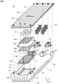
- FIG. 1 It is a disassembled perspective view which shows the state which decomposed
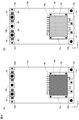
- A is an illustration figure which shows the process of mounting a power module and a base on a heat sink
- FIG. 1 is an illustration figure which shows the process of attaching a metal plate on a power module
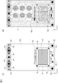
- FIG. 2 is an illustration figure which shows the process of mounting the circuit board with which the choke coil and the electrolytic capacitor were mounted on a heat sink. It is an illustration figure which shows the process of attaching a circuit board to a heat sink.
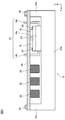
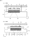
- (A) is an illustrative view showing an AA ′ section shown in FIG. 6, and (B) is an illustrative view showing a BB ′ section shown in FIG.
- FIG. 1 is an illustration figure which shows the process of attaching a metal plate on a power module
- FIG. 6 is an illustration figure which shows the process of mounting the circuit board with which the choke coil and the electrolytic capacitor were mounted on a heat sink. It is an illustration figure which shows the process of attaching a circuit board to a heat sink.
- (A) is an illustrative view showing an AA
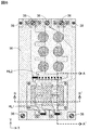
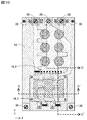
- FIG. 10 is an illustrative view showing a state where the DC / DC converter shown in FIG. 9 is seen through from above.
- (A) is an illustrative view showing a CC ′ section shown in FIG. 10
- (B) is an illustrative view showing a DD ′ section shown in FIG.
- a DC / DC converter 10 includes a heat sink 12, a power module 14 disposed above the heat sink 12, and a circuit board (above the power module 14). Substrate) 16, a plurality of choke coils (inductor elements) 18 mounted on the circuit board 16, and a plurality of electrolytic capacitors 20. When viewed from above, the outlines of the heat sink 12 and the circuit board 16 draw a rectangle of a common size.
- the X axis and the Y axis are assigned to the short side and the long side of the rectangle, respectively, and the Z axis is assigned to the direction orthogonal to the rectangle.
- the negative side and the positive side in the X-axis direction correspond to the left side and the right side, respectively
- the negative side and the positive side in the Y-axis direction correspond to the front side and the rear side, respectively
- the positive side and negative side in the Z-axis direction correspond to the upper side and Corresponds to the lower side.
- the heat sink 12 is integrated with a rectangular metal plate 12a having a concave portion CC1 on the upper surface, five metal bases 12b and two bases 12c integrally formed on the upper surface of the metal plate 12a, and a lower surface of the metal plate 12a.
- a plurality of metal-made fins 12d are formed.
- the recess CC1 is provided at a position slightly ahead of the center of the upper surface.
- the outline of the recess CC1 is rectangular, and the long side and the short side extend in the left-right direction and the front-rear direction, respectively.
- the depth of the recessed part CC1 should just be a depth which can position the module main body 14a (it mentions later for details) which comprises the power module 14.
- grease 28 is applied to the bottom surface of the recess CC1.
- four of the five pedestals 12b are respectively provided at the four corners of the upper surface of the metal plate 12a, and the other one is provided at the rear end portion of the upper surface of the metal plate 12a and at the central position in the left-right direction.
- the two pedestals 12b provided at the two rear corners are smaller than the other three pedestals 12b.
- a hole (indicated by a black circle) extending in the vertical direction is formed on the upper surface of the five pedestals 12b thus provided, and a female screw is cut on the inner peripheral surface of the hole.
- the two pedestals 12c are both formed in a band shape and are respectively provided on the left side and the right side of the recess CC1 when viewed from above.
- the length of each pedestal 12c coincides with the length of the short side of the rectangle that outlines the recess CC1, and both ends of the pedestal 12c are aligned with both ends of the short side of the rectangle.
- the height of the upper surface of each pedestal 12c is higher than the upper surface of the module main body 14a when the power module 14 is mounted in the recess CC1.
- the right side surface thereof is flush with the left inner side surface of the recess CC1.
- the left side surface of the right base 12c of the recess CC1 is flush with the right inner surface of the recess CC1.
- holes extending in the vertical direction are formed at both ends in the length direction of the upper surface, and female threads are cut on the inner peripheral surface of the hole.
- the hole (indicated by a black circle) extending in the vertical direction is additionally formed at two positions between the two pedestals 12b provided at the front end, and further, the pedestal 12b provided at the left rear end. Are additionally formed on the right side, the left side of the pedestal 12b provided at the right rear end portion, and the left side and the right side of the pedestal 12b provided at the left and right center of the rear end portion.
- the female screw is also cut into the inner peripheral surfaces of these holes.
- the plurality of fins 12d are arranged at equal intervals in the left-right direction on the lower surface of the metal plate 12a, and extend in the front-rear direction.
- the length of each fin 12d coincides with the length of the long side that outlines the metal plate 12a, and both ends in the length direction of each fin 12d are matched with both ends of the long side.
- two pedestals 24 are placed on the rear end of the upper surface of the metal plate 12a. Specifically, one pedestal 24 is placed between a pedestal 12b provided at the left rear end and a pedestal 12b provided at the left and right center of the rear end, and the other pedestal 24 is located at the left and right center of the rear end. Is placed between the pedestal 12b provided on the right and the pedestal 12b provided on the right rear end.
- Each pedestal 24 has two legs projecting to the left and right sides, and through holes (indicated by black circles) penetrating in the vertical direction are formed in each of the two legs.
- the through hole formed in this manner overlaps with the through hole formed in the rear end portion of the upper surface of the metal plate 12a when the base 24 is placed on the upper surface of the metal plate 12a.
- the power module 14 includes a module main body 14a molded with resin and a plurality of leads 14b protruding from the module main body 14a.
- the module main body 14a is formed in a rectangular parallelepiped shape, and the upper surface or the lower surface thereof is rectangular.
- the long side of the rectangle is slightly shorter than the long side of the recess CC1, and the short side of the rectangle is slightly shorter than the short side of the recess CC1.
- a part of the plurality of leads 14b protrudes forward from the front side surface of the module body 14a, and another part of the plurality of leads 14b protrudes rearward from the rear side surface of the module body 14a.
- the protruding height position is a position slightly above the center of the front side in the height direction.
- Two through holes indicated by black circles are respectively formed in two of the plurality of leads 14b protruding from the front side surface. Further, the remaining lead 14d having no through-hole is bent upward and extends upward after protruding forward or rearward.
- the two leads 14b having the through holes are arranged on the two holes formed in the front end portion of the upper surface of the metal plate 12a.
- the through hole formed in the lead 14b overlaps with the hole formed in front of the upper surface of the metal plate 12a.
- four screw members male screws are formed on the outer peripheral surface and the material is metal
- four screw members are screwed into a total of four through holes provided in the two bases 24, and Are screwed into a total of four holes formed at the rear end of the upper surface of the metal plate 12a.
- the base 24 is fixed to the metal plate 12a.
- Two screw members (a male screw is formed on the outer peripheral surface and the material is metal) 32 are screwed into two through holes formed in the lead 14b and further formed at the front end portion of the upper surface of the metal plate 12a. Screwed into the two holes.
- the two leads 14b having the through holes are fixed to the metal plate 12a.
- a rectangular heat dissipating sheet (resin member) 26 is attached to the upper surface of the module body 14a. Specifically, the lengths of the long side and the short side of the heat dissipation sheet 26 coincide with the lengths of the long side and the short side of the rectangle formed by the upper surface of the module body 14a.
- the heat dissipating sheet 26 is adhered to the upper surface of the module main body 14a so that the contour thereof overlaps the contour of the upper surface of the module main body 14a.
- the metal plate 22 is attached to the base 12c after the power module 14 is fitted into the recess CC1 and the heat dissipation sheet 26 is attached to the upper surface of the module body 14a.
- the outline of the metal plate 22 is a rectangle, and the length of the long side thereof is the same as the distance from the left side surface of the left pedestal 12c to the right side surface of the right pedestal 12c.
- the length of the short side of the said rectangle corresponds with the length of the base 12c.
- an opening OP1 that opens in the vertical direction is formed in the center of the metal plate 22 in the center of the metal plate 22 in the center of the metal plate 22, an opening OP1 that opens in the vertical direction is formed.
- the opening OP1 is also rectangular, and its long side extends in the left-right direction, while its short side extends in the front-rear direction.
- Through holes (shown by black circles) reaching the lower surface of the metal plate 22 are formed at the four corners of the upper surface of the metal plate 22, and female threads are cut on the inner peripheral surface of the through hole.
- the metal plate 22 has a left side that is flush with the left side of the left pedestal 12c and a right side that is flush with the right side of the right pedestal 12c. It mounts on the two bases 12c so that it may become.
- the four through holes formed in the metal plate 22 respectively overlap with the total of four holes formed in the two bases 12c.
- Four screw members (a male screw is formed on the outer peripheral surface and the material is metal) 34 are screwed into four through holes formed in the metal plate 22, and further, a total of four screws formed on the two bases 12c. Screwed into the hole.
- the metal plate 22 is fixed to the pedestal 12c.
- the power module 14 is pressed against the heat sink 12 by the metal plate 22 thus fixed.
- seven through holes reaching the lower surface of the circuit board 16 are formed at the end of the upper surface of the circuit board 16. Among these, four through holes are formed at the four corners, and the three through holes are formed at the rear end portion so as to be lined up on the left and right.
- circuit patterns PT1 to PT3 are formed on the lower surface of the circuit board 16.
- the four choke coils 18 and the six electrolytic capacitors 20 are mounted on the lower surface of the circuit board 16 having such a structure.
- the choke coil 18 is arranged at a position overlapping the opening OP1 as viewed from above.
- the electrolytic capacitor 20 is disposed at a position between the rear side surface of the module main body 14a and the base 12b or 24 as viewed from above.
- the seven through holes formed in the end portion of the circuit board 16 respectively overlap a total of seven holes formed in the five bases 12b and the two bases 24. Furthermore, the through hole HL1 or HL2 formed on the upper surface of the circuit board 16 overlaps the tip of the lead 14b bent upward.
- five screw members male screws are formed on the outer peripheral surface and the material is metal
- two screw members male screws are formed on the outer peripheral surface and the material is metal
- 38 are the circuit board. 16 is screwed into seven through holes, and is further screwed into a total of seven holes formed in the five bases 12 b and the two bases 24. As a result, the circuit board 16 is fixed to the heat sink 12, and the lead 14b protrudes above the circuit board 16 through the through hole HL1 or HL2.
- the AA ′ cross section shown in FIG. 6 has the structure shown in FIG. 7A
- the BB ′ cross section shown in FIG. 6 has the structure shown in FIG. 7B.
- the heights of the pedestals 12b and 24 are adjusted to a height at which a gap is formed between the lower end surface of the choke coil 18 and the upper surface of the module body 14a when the circuit board 16 is fixed to the heat sink 12. Moreover, the thickness of the heat dissipation sheet 26 in the natural state is adjusted to a thickness that exceeds the height of the gap. Therefore, in a state where the circuit board 16 is fixed to the heat sink 12, the heat dissipation sheet 26 is continuously pressed by the choke coil 18.
- the heat generated by the choke coil 18 is transmitted to the heat radiating sheet 26 thus pressed, and then released to the outside through the module main body 14a and the heat sink 12 (strictly, the metal plate 12a and the fin 12d). It is discharged to the outside through the plate 22 and the heat sink 12 (strictly speaking, the pedestal 12c, the metal plate 12a and the fins 12d).
- the heat generated in the module body 14a is released from the fins 12d through the metal plate 12a.
- FIG. 8 shows an equivalent circuit of the DC / DC converter 10 having such a structure.
- the inductor L1 is realized by the choke coil 18, and the capacitors C1 and C2 are realized by the electrolytic capacitor 20.
- the control circuit CTR1 and the field effect transistors TR1 and TR2 are provided in the module body 14a.
- the input terminal Tin is connected to one end of each of the capacitors C1 and C2 and the drain of the transistor TR2.
- the source of the transistor TR2 is connected to the drain of the transistor TR1 and one end of the inductor L1.
- the ground terminal Tgnd is connected to the other end of the capacitor C1 and the source of the transistor TR1.
- the output terminal Tout is connected to the other end of the capacitor C2 and the other end of the inductor L1.
- the gates of the transistors TR1 and TR2 are connected to the control circuit CTR1.
- the DC / DC converter 10 includes the heat sink 12, the power module 14 disposed above the heat sink 12, the circuit board 16 disposed above the power module 14, and the circuit board 16. And a mounted choke coil 18.
- the power module 14 is attached to the heat sink 12 by a metal plate 22. More specifically, the metal plate 22 has an opening OP ⁇ b> 1 that opens in the vertical direction, and presses the power module 14 against the heat sink 12.
- the circuit board 16 is held by the bases 12b and 24 and the screw members 36 and 38 so that the choke coil 18 protrudes downward and overlaps the power module 14 and the opening OP1 in plan view.
- the heat dissipation sheet 26 is disposed below the choke coil 18 so as to be in contact with each of the choke coil 18 and the metal plate 22. More specifically, the heat dissipation sheet 26 is disposed between the metal plate 22 and the power module 14, and the choke coil 18 contacts the heat dissipation sheet 26 through the opening OP1.
- the choke coil 18 mounted on the circuit board 16 overlaps the power module 14 in plan view. Thereby, the planar size of the DC / DC converter 10 can be suppressed.
- the heat dissipation sheet 26 contacts the choke coil 18 mounted on the circuit board 16 and contacts the metal plate 22 that attaches the power module 14 to the heat sink 12. As described above, the heat generated in the choke coil 18 is transmitted from the heat dissipation sheet 26 to the heat sink 12 via the module main body 14a and the metal plate 22, and then released to the outside. Thereby, the heat dissipation performance can be enhanced.
- the metal plate 22 is formed with an opening OP1 that opens in the vertical direction, and the choke coil 18 contacts the heat dissipation sheet 26 through the opening OP1, so that the DC / DC converter 10 can be reduced in height.
- a flat metal plate 22 ′ having no opening OP1 is adopted instead of the metal plate 22, Except for the fact that the heat dissipating sheets 26a and 26b are employed instead of the heat dissipating sheet 26, the structure is the same as that of the DC / DC converter 10 described above. Therefore, the overlapping description regarding the same structure is omitted as much as possible.
- the outline of the metal plate 22 ' is rectangular, and the length of the long side thereof coincides with the distance from the left side surface of the left pedestal 12c to the right side surface of the right pedestal 12c. Moreover, the length of the short side of the said rectangle corresponds with the length of the base 12c.
- Through holes (shown by black circles) reaching the lower surface of the metal plate 22 ' are formed at the four corners of the upper surface of the metal plate 22', and female screws are cut on the inner peripheral surface of the through hole.
- the power module 14 is pressed against the heat sink 12 by such a metal plate 22 ′.
- each of the heat dissipation sheets 26a and 26b matches the shape of the heat dissipation sheet 26. Specifically, the lengths of the long side and the short side of the heat radiation sheets 26a and 26b coincide with the lengths of the long side and the short side of the rectangle formed by the upper surface of the module body 14a.
- the heat dissipation sheet 26a is adhered to the center of the upper surface of the metal plate 22 ′, and the heat dissipation sheet 26b is adhered to the center of the lower surface of the metal plate 22 ′.
- the long sides of the heat radiation sheets 26a and 26b extend in the left-right direction, and the short sides of the heat radiation sheets 26a and 26b extend in the front-rear direction.
- the cross section CC ′ shown in FIG. 10 has the structure shown in FIG. 11A
- the cross section DD ′ shown in FIG. 10 has the structure shown in FIG.
- the height of the bases 12b and 24 and the thickness of the metal plate 22 ′ are such that a gap is formed between the lower end surface of the choke coil 18 and the upper surface of the metal plate 22 ′ when the circuit board 16 is fixed to the heat sink 12. Adjusted to Further, the thickness of the heat dissipation sheet 26a in the natural state is adjusted to a thickness exceeding the height of the gap. Therefore, in a state where the circuit board 16 is fixed to the heat sink 12, the heat dissipation sheet 26 a is continuously pressed by the choke coil 18.
- the heat generated in the choke coil 18 is transmitted to the heat radiating sheet 26a thus pressed, and then the metal plate 22 ', the heat radiating sheet 26b, the module body 14a, and the heat sink 12 (strictly, the metal plate 12a and the fin 12d)
- the metal plate 22 ′ and the heat sink 12 are discharged to the outside.
- the base 12c, the metal plate 12a, and the fins 12d are discharged to the outside.
- most of the heat generated in the choke coil 18 is released to the outside through the latter heat dissipation path.
- the heat generated in the module main body 14a is released from the fins 12d through the metal plate 12a, and is released to the heat sink 12 through the heat radiating sheet 26b and the metal plate 22 '.
- a flat metal plate 22 ' is employed, and the heat dissipation sheet 26a is disposed between the choke coil 18 and the metal plate 22'.
- the areas of the upper and lower surfaces of the metal plate 22 ′ are larger than the areas of the upper and lower surfaces of the metal plate 22 by the amount that the opening OP1 is not formed. For this reason, compared with the DC / DC converter 10 which employ
- the non-insulated DC / DC converter 10 or 10 ' is assumed, but the present invention can also be applied to an insulated DC / DC converter.
- a transformer is assumed as the inductor element.
- the switching element is provided in the power module.
Landscapes
- Engineering & Computer Science (AREA)
- Microelectronics & Electronic Packaging (AREA)
- Physics & Mathematics (AREA)
- Thermal Sciences (AREA)
- Dc-Dc Converters (AREA)
Abstract
Description
図1および図2を参照して、この実施例のDC/DCコンバータ10は、ヒートシンク12と、ヒートシンク12の上方に配されたパワーモジュール14と、パワーモジュール14の上方に配された回路基板(基板)16と、回路基板16に実装された複数のチョークコイル(インダクタ素子)18および複数の電解コンデンサ20とを備える。上方から眺めたとき、ヒートシンク12および回路基板16の各々の輪郭は共通のサイズの長方形を描く。
[実施例2]
12 …ヒートシンク
12a …金属板
12b …台座(保持部材の一部)
12c …台座
14 …パワーモジュール
14a …モジュール本体
14b …リード
16 …回路基板(基板)
18 …チョークコイル(インダクタ素子)
22,22´ …金属板(取り付け部材)
24 …台座(保持部材の一部)
26,26a …放熱シート(樹脂部材)
26b …放熱シート(追加の樹脂部材)
28 …グリス
36,38 …螺子部材(保持部材の他の一部)
OP1 …開口部
Claims (3)
- ヒートシンクと、
前記ヒートシンクの上方に配されたパワーモジュールと、
前記パワーモジュールの上方に配された基板と、
前記基板に実装されたインダクタ素子と、
を備えるDC/DCコンバータであって、
前記パワーモジュールを前記ヒートシンクに取り付ける金属製の取り付け部材と、
前記インダクタ素子が下方に突出しかつ平面視で前記パワーモジュールと重なるように前記基板を保持する保持部材と、
前記インダクタ素子および前記取り付け部材の各々と接触するように前記インダクタ素子の下方に配された樹脂部材と、
をさらに備える、DC/DCコンバータ。 - 前記取り付け部材は上下方向に開口する開口部を有して前記パワーモジュールを前記ヒートシンクに押圧する金属板を含み、
前記樹脂部材は前記金属板と前記パワーモジュールとの間に配され、
前記インダクタ素子は前記開口部を通して前記樹脂部材と接触する、請求項1記載のDC/DCコンバータ。 - 前記取り付け部材は前記パワーモジュールを前記ヒートシンクに押圧する平坦な金属板を含み、
前記樹脂部材は前記金属板と前記インダクタ素子との間に配され、
前記取り付け部材と前記パワーモジュールとの間に追加の樹脂部材が配される、請求項1記載のDC/DCコンバータ。
Priority Applications (3)
| Application Number | Priority Date | Filing Date | Title |
|---|---|---|---|
| CN201680076358.XA CN108432113B (zh) | 2016-01-08 | 2016-12-16 | Dc/dc转换器 |
| DE112016005575.7T DE112016005575T5 (de) | 2016-01-08 | 2016-12-16 | DC-DC-Wandler |
| JP2017560080A JP6399240B2 (ja) | 2016-01-08 | 2016-12-16 | Dc/dcコンバータ |
Applications Claiming Priority (2)
| Application Number | Priority Date | Filing Date | Title |
|---|---|---|---|
| JP2016002471 | 2016-01-08 | ||
| JP2016-002471 | 2016-01-08 |
Publications (1)
| Publication Number | Publication Date |
|---|---|
| WO2017119261A1 true WO2017119261A1 (ja) | 2017-07-13 |
Family
ID=59273697
Family Applications (1)
| Application Number | Title | Priority Date | Filing Date |
|---|---|---|---|
| PCT/JP2016/087478 Ceased WO2017119261A1 (ja) | 2016-01-08 | 2016-12-16 | Dc/dcコンバータ |
Country Status (4)
| Country | Link |
|---|---|
| JP (1) | JP6399240B2 (ja) |
| CN (1) | CN108432113B (ja) |
| DE (1) | DE112016005575T5 (ja) |
| WO (1) | WO2017119261A1 (ja) |
Cited By (2)
| Publication number | Priority date | Publication date | Assignee | Title |
|---|---|---|---|---|
| WO2021096305A1 (ko) * | 2019-11-13 | 2021-05-20 | 엘지이노텍 주식회사 | 컨버터 |
| JP2024059088A (ja) * | 2022-10-17 | 2024-04-30 | トヨタ モーター エンジニアリング アンド マニュファクチャリング ノース アメリカ,インコーポレイティド | パワーエレクトロニクスデバイスを組み込んだパワーエレクトロニクスアセンブリ |
Families Citing this family (1)
| Publication number | Priority date | Publication date | Assignee | Title |
|---|---|---|---|---|
| CN114424683B (zh) * | 2019-09-12 | 2025-08-26 | 索尤若驱动有限及两合公司 | 电子设备和用于由组合部件制造第一和第二电子设备的方法 |
Citations (2)
| Publication number | Priority date | Publication date | Assignee | Title |
|---|---|---|---|---|
| JP2011193000A (ja) * | 2010-03-16 | 2011-09-29 | Intersil Americas Inc | 他の部品上にブリッジインダクタを備えたモールド電源モジュール及びその製造方法 |
| WO2015019519A1 (ja) * | 2013-08-07 | 2015-02-12 | パナソニックIpマネジメント株式会社 | Dc-dcコンバータモジュール |
Family Cites Families (2)
| Publication number | Priority date | Publication date | Assignee | Title |
|---|---|---|---|---|
| JP2010232391A (ja) * | 2009-03-26 | 2010-10-14 | Panasonic Electric Works Co Ltd | 電気回路装置 |
| JP5396446B2 (ja) * | 2011-08-30 | 2014-01-22 | 日立オートモティブシステムズ株式会社 | 車載用電源装置 |
-
2016
- 2016-12-16 JP JP2017560080A patent/JP6399240B2/ja active Active
- 2016-12-16 WO PCT/JP2016/087478 patent/WO2017119261A1/ja not_active Ceased
- 2016-12-16 CN CN201680076358.XA patent/CN108432113B/zh active Active
- 2016-12-16 DE DE112016005575.7T patent/DE112016005575T5/de not_active Ceased
Patent Citations (2)
| Publication number | Priority date | Publication date | Assignee | Title |
|---|---|---|---|---|
| JP2011193000A (ja) * | 2010-03-16 | 2011-09-29 | Intersil Americas Inc | 他の部品上にブリッジインダクタを備えたモールド電源モジュール及びその製造方法 |
| WO2015019519A1 (ja) * | 2013-08-07 | 2015-02-12 | パナソニックIpマネジメント株式会社 | Dc-dcコンバータモジュール |
Cited By (5)
| Publication number | Priority date | Publication date | Assignee | Title |
|---|---|---|---|---|
| WO2021096305A1 (ko) * | 2019-11-13 | 2021-05-20 | 엘지이노텍 주식회사 | 컨버터 |
| US12219742B2 (en) | 2019-11-13 | 2025-02-04 | Lg Innotek Co., Ltd. | Converter including heat transfer layer |
| KR102937316B1 (ko) * | 2019-11-13 | 2026-03-10 | 엘지이노텍 주식회사 | 컨버터 |
| JP2024059088A (ja) * | 2022-10-17 | 2024-04-30 | トヨタ モーター エンジニアリング アンド マニュファクチャリング ノース アメリカ,インコーポレイティド | パワーエレクトロニクスデバイスを組み込んだパワーエレクトロニクスアセンブリ |
| JP7659025B2 (ja) | 2022-10-17 | 2025-04-08 | トヨタ モーター エンジニアリング アンド マニュファクチャリング ノース アメリカ,インコーポレイティド | パワーエレクトロニクスデバイスを組み込んだパワーエレクトロニクスアセンブリ |
Also Published As
| Publication number | Publication date |
|---|---|
| JP6399240B2 (ja) | 2018-10-03 |
| CN108432113B (zh) | 2019-07-12 |
| JPWO2017119261A1 (ja) | 2018-09-20 |
| DE112016005575T5 (de) | 2018-08-23 |
| CN108432113A (zh) | 2018-08-21 |
Similar Documents
| Publication | Publication Date | Title |
|---|---|---|
| CN108702856B (zh) | 电路构成体 | |
| JP2018186143A (ja) | 回路基板モジュール、電子装置 | |
| JP2002290087A (ja) | オンボード実装型電子機器およびオンボード実装型電源装置 | |
| CN108352691B (zh) | 电路结构体及电气接线盒 | |
| KR20140026612A (ko) | 열관리 특징부를 갖는 전자 디바이스 인클로져 및 히트 싱크 구조체 | |
| JP6399240B2 (ja) | Dc/dcコンバータ | |
| US20200404803A1 (en) | Circuit assembly and electrical junction box | |
| WO2020054376A1 (ja) | 電力変換器 | |
| WO2017038419A1 (ja) | 回路構成体および電気接続箱 | |
| US10840178B2 (en) | Circuit assembly and mounting unit | |
| JP2012009498A (ja) | 発熱体の放熱構造と放熱構造を備えたオーディオアンプ | |
| JP2021002627A5 (ja) | ||
| JP4998373B2 (ja) | 絶縁シート、電源回路、及び電子機器 | |
| US20210368618A1 (en) | Circuit assembly and electrical junction box | |
| JP2012239283A (ja) | 電源装置 | |
| JP2015104183A (ja) | 回路構成体およびdc−dcコンバータ装置 | |
| JP2015082960A (ja) | Dc−dcコンバータ装置 | |
| JP2019087729A (ja) | 回路組立体及び実装ユニット | |
| JP7172471B2 (ja) | 基板構造体 | |
| CN116235297A (zh) | 基板单元 | |
| CN111180401B (zh) | 散热部件及电连接箱 | |
| JP2014212289A (ja) | 電源装置 | |
| JP4565422B2 (ja) | 電子部品の放熱板 | |
| JP2018174218A (ja) | 発熱部品の固定構造および発熱部品の固定方法 | |
| KR101801195B1 (ko) | 조명모듈 제조방법 및 이에 의하여 제조되는 조명모듈 |
Legal Events
| Date | Code | Title | Description |
|---|---|---|---|
| 121 | Ep: the epo has been informed by wipo that ep was designated in this application |
Ref document number: 16883761 Country of ref document: EP Kind code of ref document: A1 |
|
| ENP | Entry into the national phase |
Ref document number: 2017560080 Country of ref document: JP Kind code of ref document: A |
|
| WWE | Wipo information: entry into national phase |
Ref document number: 112016005575 Country of ref document: DE |
|
| 122 | Ep: pct application non-entry in european phase |
Ref document number: 16883761 Country of ref document: EP Kind code of ref document: A1 |