WO2017119092A1 - 電流検出装置及び補正係数算出方法 - Google Patents
電流検出装置及び補正係数算出方法 Download PDFInfo
- Publication number
- WO2017119092A1 WO2017119092A1 PCT/JP2016/050302 JP2016050302W WO2017119092A1 WO 2017119092 A1 WO2017119092 A1 WO 2017119092A1 JP 2016050302 W JP2016050302 W JP 2016050302W WO 2017119092 A1 WO2017119092 A1 WO 2017119092A1
- Authority
- WO
- WIPO (PCT)
- Prior art keywords
- bus bars
- current
- correction coefficient
- magnetic
- magnetic detection
- Prior art date
- Legal status (The legal status is an assumption and is not a legal conclusion. Google has not performed a legal analysis and makes no representation as to the accuracy of the status listed.)
- Ceased
Links
Images



Classifications
-
- G—PHYSICS
- G01—MEASURING; TESTING
- G01R—MEASURING ELECTRIC VARIABLES; MEASURING MAGNETIC VARIABLES
- G01R15/00—Details of measuring arrangements of the types provided for in groups G01R17/00 - G01R29/00, G01R33/00 - G01R33/26 or G01R35/00
- G01R15/14—Adaptations providing voltage or current isolation, e.g. for high-voltage or high-current networks
- G01R15/20—Adaptations providing voltage or current isolation, e.g. for high-voltage or high-current networks using galvano-magnetic devices, e.g. Hall-effect devices, i.e. measuring a magnetic field via the interaction between a current and a magnetic field, e.g. magneto resistive or Hall effect devices
-
- G—PHYSICS
- G01—MEASURING; TESTING
- G01R—MEASURING ELECTRIC VARIABLES; MEASURING MAGNETIC VARIABLES
- G01R15/00—Details of measuring arrangements of the types provided for in groups G01R17/00 - G01R29/00, G01R33/00 - G01R33/26 or G01R35/00
- G01R15/14—Adaptations providing voltage or current isolation, e.g. for high-voltage or high-current networks
- G01R15/20—Adaptations providing voltage or current isolation, e.g. for high-voltage or high-current networks using galvano-magnetic devices, e.g. Hall-effect devices, i.e. measuring a magnetic field via the interaction between a current and a magnetic field, e.g. magneto resistive or Hall effect devices
- G01R15/207—Constructional details independent of the type of device used
-
- G—PHYSICS
- G01—MEASURING; TESTING
- G01R—MEASURING ELECTRIC VARIABLES; MEASURING MAGNETIC VARIABLES
- G01R19/00—Arrangements for measuring currents or voltages or for indicating presence or sign thereof
- G01R19/0092—Measuring current only
-
- G—PHYSICS
- G01—MEASURING; TESTING
- G01R—MEASURING ELECTRIC VARIABLES; MEASURING MAGNETIC VARIABLES
- G01R35/00—Testing or calibrating of apparatus covered by the other groups of this subclass
- G01R35/005—Calibrating; Standards or reference devices, e.g. voltage or resistance standards, "golden" references
Definitions
- the present invention relates to a current detection device and a correction coefficient calculation method.
- a current measuring device described in Patent Document 1 is a reading unit that reads output signals of four magnetic field sensors arranged so as to sandwich each conductor of a conductor array composed of three conductors arranged in parallel to each other. And an arithmetic unit for calculating a current flowing through each conductor based on an output signal read by the reading unit and a correction coefficient representing an influence of a predetermined magnetic field on the output signal of each magnetic field sensor.
- the correction coefficient used for the calculation of the calculation unit is calculated and recorded in advance in a state where only one conductor is energized and the other conductor is not energized.
- an object of the present invention is to provide a current detection device and a correction coefficient calculation method capable of detecting a current flowing in a bus bar covered with a magnetic shield with high accuracy.
- the present invention is arranged corresponding to each of a plurality of bus bars and the plurality of bus bars, detects the intensity of a magnetic field generated by a current flowing through the bus bar, and determines the intensity of the magnetic field.
- a plurality of magnetic detection elements that output a corresponding voltage, a magnetic shield disposed so as to surround a part of the plurality of bus bars and the plurality of magnetic detection elements, and any two or more of the plurality of bus bars
- the current flowing through the bus bar can be detected with high accuracy in a configuration in which the bus bar is covered with the magnetic shield.
- FIG. 2 is a sectional view taken along line AA in FIG. 1. It is a graph which shows the measurement result of the voltage output of a magnetic detection element when it supplies with electricity only to the U phase. It is a graph which shows the measurement result of the voltage output of a magnetic detection element when it supplies with electricity to U phase and V phase. It is a graph which shows the measurement result of the voltage output of a magnetic detection element when the electric current in which the magnitude
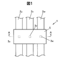
- FIG. 1 is a plan view of a main part showing a current detection device according to an embodiment of the present invention.
- 2 is a cross-sectional view taken along line AA in FIG.
- an arithmetic unit and a correction coefficient storage unit which will be described later are not shown.
- the current detection device 1 includes a plurality of bus bars 2u, 2v, 2w (in the present embodiment, three for three phases) arranged in parallel (hereinafter collectively referred to as “the three”).
- bus bar 2 "Also referred to as” bus bar 2 ") and three bus bars 2u, 2v, 2w, which are arranged corresponding to each of the bus bars 2u, 2v, 2w, detect the intensity of the magnetic field generated by the current flowing through the bus bars 2u, 2v, 2w, and the detected magnetic field intensity
- a plurality of (three in the present embodiment) magnetic detection elements 3u, 3v, 3w (hereinafter also collectively referred to as “magnetic detection element 3”) and three bus bars 2u that output a voltage corresponding to , 2v, 2w, and the mold resin part 4 covering the three magnetic detection elements 3u, 3v, 3w, the magnetic shield 5 covering the periphery of the mold resin part 4, and the three magnetic detection elements 3u, 3v, Based on the
- the bus bar 2 is formed of a plate-like conductor and serves as a current path through which a three-phase AC motor current flows between a motor that is a driving source for driving an automobile and an inverter, for example.
- the current flowing through the bus bar 2 is, for example, about 200 A at the maximum in a steady state, about 800 A at the inrush current in an abnormal state, and the frequency is, for example, about 100 kHz at the maximum.
- the three bus bars 2 are arranged on the same plane and are arranged in parallel at equal intervals in the width direction so that the longitudinal directions thereof are parallel to each other. When a current flows through the bus bar, a magnetic field is generated in a direction orthogonal to the direction of the current, and its strength decreases as the distance from the bus bar increases.
- the magnetic detection element 3 is configured to output a voltage corresponding to the strength (magnetic flux density) of the magnetic field in the direction along the detection axis.
- an MR (Magneto Resistance) sensor such as a GMR (Giant Magneto Resistive effect) sensor can be used.
- GMR Magnetic Magneto Resistive effect
- a GMR sensor with relatively high sensitivity is used. Since the magnetic detection element 3 has a different magnetic field to be detected depending on the position with respect to the bus bar 2, the output is different even when the same current flows in the corresponding bus bar.
- the magnetic detection element 3 is disposed, for example, in contact with or close to the bus bar 2.
- the direction of the magnetic detection element 3 is preferably a direction in which the detection axis is orthogonal to the longitudinal direction of the bus bar 2, but may be inclined from the orthogonal direction.
- a through hole may be formed in the bus bar 2 and the magnetic detection element 3 may be disposed in the through hole.
- the mold resin portion 4 for example, an epoxy resin having high electrical insulation is used.
- the magnetic shield 5 shields the entire three bus bars 2 at a time in order to eliminate the influence of disturbance due to an external magnetic field.
- the magnetic shield 5 is formed using, for example, a soft magnetic material such as permalloy, an electromagnetic steel plate, or ferrite. Since the magnetic permeability of the magnetic shield 5 is sufficiently larger than 1 (generally 1000 or more), the magnetic flux of the disturbance magnetic field is attracted to the magnetic shield 5, so that the magnetic field strength at the installation location of the magnetic detection element 3 can be reduced. (Disturbance shield effect).
- the magnetic flux generated when the bus bar 2 is energized is attracted to the magnetic shield 5.
- the relative permeability of the magnetic shield 5 changes due to the effect of the magnetic field inside the magnetic shield 5. For example, when the magnetic field inside the magnetic shield 5 increases, the change in the magnetic flux density decreases with respect to the change in the magnetic field (so-called saturation). ), The relative permeability is reduced.
- the relative permeability of the magnetic shield 5 changes, the degree to which the magnetic flux is attracted to the magnetic shield 5 changes, so that the magnetic field strength at the position of the magnetic detection element 3 changes.
- a current is applied to a plurality of bus bars of the bus bar 2
- the magnetic flux inside the magnetic shield 5 is obtained by superimposing the influences of the plurality of bus bars.
- the magnetic shield 5 is installed so as to surround the bus bar 2, but it is not always necessary to have a closed shape, and a gap of a certain size may be open. Furthermore, the structure which arrange
- the calculation unit 6 obtains the magnetic flux density from the voltage output from the magnetic detection element 3 using a relational expression that connects the two, calculates a current flowing through each bus bar 2 from the obtained magnetic flux density, and the magnetic detection element. And a correction coefficient calculation unit 62 that calculates a correction coefficient for correcting the interference between the three.
- the calculation unit 6 can be realized by an integrated circuit (IC) such as ASIC (Application Specific Integrated Circuit) or FPGA (Field Programmable Gate Array).
- the current calculation unit 61 calculates the current flowing through each bus bar 2 using the following formula (1), for example.
- Vu, Vv, and Vw are voltages output by the magnetic detection elements 3u, 3v, and 3w, respectively
- Bu, Bv, and Bw are magnetic flux densities obtained by converting the voltages of the respective phases into functions fu, fv, and fw.
- a 11 to a 33 are correction coefficients
- Iu, Iv, and Iw are currents flowing through the bus bars 2u, 2v, and 2w, respectively.
- Iu, Iv, and Iw may be voltages proportional to currents flowing through the bus bars 2u, 2v, and 2w, respectively.
- the correction coefficient storage unit 7 is, for example, an EEPROM of a nonvolatile memory, and stores correction coefficients a 11 to a 33 for correcting interference between the magnetic detection elements 3.
- the correction coefficient calculation unit 62 obtains an optimal correction coefficient and stores it in the correction coefficient storage unit 7. Then, the current calculation unit 61 calculates the current flowing through each bus bar 2 by substituting the correction coefficient stored in the correction coefficient storage unit 7 into the equation (1).
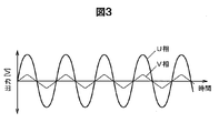
- FIG. 3 is a graph showing the output measurement results when only the U phase is energized.
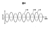
- FIG. 4 is a graph showing the output measurement results when the U phase and V phase are energized.
- each magnetic detection element 3 Since each magnetic detection element 3 is close to each other, it is affected by another phase different from the target phase (mutual interference). For this reason, each magnetic detection element 3 detects a magnetic field obtained by synthesizing the magnetic fields generated by the currents flowing through the respective bus bars 2. For this reason, in order to accurately calculate the current flowing individually in the bus bar 2, it is necessary to correct the interference using a correction coefficient.
- the magnetic field generated around the energized bus bar 2 varies greatly depending on the current of the energized bus bar 2. Since the magnetic field inside the magnetic shield 5 also fluctuates greatly accordingly, the relative permeability of the magnetic shield 5 changes in accordance with the change in current, so that the magnetic detection corresponding to the bus bar 2 other than the energized bus bar 2 is detected.
- the output voltage of the element 3 is non-linear. Note that the output voltage of the magnetic detection element 3 corresponding to the energized bus bar 2 is influenced by the change in the relative permeability of the magnetic shield 5 because the position of the magnetic detection element 3 is arranged close to the bus bar 2. The output is linear. For example, as shown in FIG.
- a current having a substantially the same amplitude and opposite phase is applied to any two phases with the magnetic shield 5 incorporated.
- the fluctuation of the magnetic field in the magnetic shield 5 can be suppressed to be small, the output voltage of the magnetic detection element 3 becomes linear, and an accurate correction coefficient can be calculated.
- the correction coefficient is obtained by reducing the amplitude of the sum of the currents to be supplied to the bus bar 2 installed inside the magnetic shield 5, so that, for example, even if the three phases of the bus bar 2 are supplied simultaneously, If the amplitude of the sum of the currents is small, the effect of the present invention can be obtained.
- highly accurate interference correction between the magnetic detection elements 3 becomes possible.
- the correction factor when measuring three-phase current is a 3 ⁇ 3 matrix, and three independent measurements are required to uniquely define all elements.
- the output linear pressure of the magnetic detection element 3 is measured by supplying currents having substantially the same amplitude and opposite phases in the combination of the U phase and the V phase, and then the combination of the U phase, the V phase, and the W phase.
- the current is applied to the U phase and the W phase with reference to the V phase and the current is opposite in phase and the sum of the amplitudes is substantially the same as the V phase, and the output voltage of the magnetic detection element 3 is measured.
- a highly accurate correction coefficient can be calculated by measuring the output voltage of the magnetic detection element 3 by applying currents having substantially the same amplitude and opposite phases in the combination of the U phases.
- the amplitude difference between them is It is preferable to set it to 1/10 or less of the larger one in calculating the correction coefficient with high accuracy.
- the amplitudes Vuo_i, Vvo_i, Vwo_i of the voltages output from the detection elements 3u, 3v, 3w are acquired.
- the reference current Iu is supplied to the U-phase bus bar 2u
- the amplitudes Iuo_i, Ivo_i, Iwo_i of the currents (reference currents) flowing through the bus bars 2u, 2v, 2w are measured (Iwo_i is zero).
- the reference current Iv is supplied to the V-phase bus bar 2v, and the U-phase bus bar 2u has an amplitude that is k (0 ⁇ k ⁇ 0.5) times opposite to that of the V-phase.
- the voltages Vuo_ii, Vvo_ii, and Vwo_ii output from 3u, 3v, and 3w are acquired.
- the amplitudes Iuo_ii, Ivo_ii, and Iwo_ii of the currents (reference currents) flowing through the bus bars 2u, 2v, and 2w are measured.
- the reference current Iw is supplied to the W-phase bus bar 2w
- the reverse-phase current Iv is supplied to the V-phase bus bar 2v with substantially the same amplitude as the W-phase.
- the voltages Vuo_iii, Vvo_iii, and Vwo_iii output from the magnetic detection elements 3u, 3v, and 3w are acquired.
- the amplitudes Iuo_iii, Ivo_iii, and Iwo_iii of the currents (reference currents) flowing through the bus bars 2u, 2v, and 2w are measured (Iuo_iii is zero).
- the current amplitude matrix on the left side of Equation (2) is I N
- the coefficient (scalar value) for converting the voltage value that is the first factor on the right side to the current value is G
- the interference correction coefficient matrix that is the second factor is A
- 3 is a factor output gradient matrix
- I N GAV G (3) It can be expressed.
- the current amplitude matrix I N is a current amplitude obtained by normalizing the measured current amplitude with a reference current.
- the output gradient matrix V G is a voltage amplitude obtained by normalizing the output voltage amplitude with a reference current.
- FIG. 5 is a graph showing a measurement result of the output voltage of the magnetic detection element 3 when currents having substantially the same amplitude and opposite phases are applied to the U-phase and V-phase bus bars.
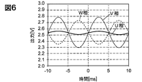
- FIG. 6 is a graph showing measurement results of the output voltage of the magnetic detection element 3 when currents having substantially the same amplitude and opposite phases are applied to the V-phase and W-phase bus bars.
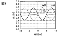
- FIG. 7 is a graph showing the measurement results of the voltage output of the magnetic detection element 3 when currents having substantially the same amplitude and opposite phases are applied to the W-phase and U-phase bus bars.
- the output voltage of the magnetic detection elements 3u and 3v is a large sine wave, but the W-phase magnetism is not energized.
- the output voltage of the detection element 3w is a small sine wave.
- the output voltage of the magnetic detection elements 3v and 3w is a large sine wave, but the U-phase magnetism is not energized.
- the output voltage of the detection element 3u is a small sine wave.
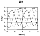
- FIG. 8 shows the measurement result of the output voltage of the magnetic detection element when the current having the same amplitude is applied to the three-phase bus bar before applying the interference correction using the correction coefficient shown in [Equation 3].
- FIG. 9 shows the measurement result of the output voltage of the magnetic detection element when the current having the same amplitude is applied to the three-phase bus bar after applying the interference correction using the correction coefficient shown in [Equation 3].
- a plurality of bus bars (2) and a plurality of bus bars (2) are arranged corresponding to each of the plurality of bus bars (2) to detect the intensity of a magnetic field generated by a current flowing through the bus bar (2), A plurality of magnetic detecting elements (3) for outputting a corresponding voltage, and a magnetic shield (5) disposed so as to surround a part of the plurality of bus bars (2) and the plurality of magnetic detecting elements (3).
- the plurality of magnetic detection elements (3) on the basis of the voltage output, current calculation unit for calculating the current flowing through the plurality of bus bars (2) and (61), a current detection device equipped with.
- a plurality of bus bars (2) and a plurality of bus bars (2) are arranged corresponding to each of the plurality of bus bars (2) to detect the strength of the magnetic field generated by the current flowing through the bus bar (2), A plurality of magnetic detection elements (3) for outputting a corresponding voltage value, and a magnetic shield (5) arranged so as to surround a part of the plurality of bus bars (2) and the plurality of magnetic detection elements (3)
- a correction coefficient calculation method in a current detection apparatus comprising: a plurality of the plurality of bus bars (2) when a current having an opposite phase is supplied to any two or more bus bars (2).
- a correction coefficient calculation method including a step of calculating a correction coefficient for correcting mutual interference of the plurality of magnetic detection elements (3) based on a voltage output from the magnetic detection element (3).
- the amplitude difference between the two current amplitudes obtained by adding the currents having opposite phases to the two or more bus bars (2) in the same phase is larger in amplitude.
- the present invention can be implemented by being modified as appropriate without departing from the spirit of the present invention.
- the correction coefficient calculated by the correction coefficient calculation unit 62 is stored in the correction coefficient storage unit 7, but the correction coefficient is recorded on a recording medium such as a sheet by printing or the like, and attached to the current detection device 1. It may be shipped to the user as a document and stored in the correction coefficient storage unit 7 by the user.
- the said embodiment demonstrated the case where the number of the bus bars 2 in which a part of longitudinal direction was enclosed by the magnetic body shield 5 was 3, the number of this bus bars 2 may be larger than three. That is, the present invention can be applied to the case where the current of a conductive path in which the number of bus bars 2 whose part in the longitudinal direction is surrounded by the magnetic shield 5 is 3 or more is detected.
Landscapes
- Physics & Mathematics (AREA)
- General Physics & Mathematics (AREA)
- Measuring Instrument Details And Bridges, And Automatic Balancing Devices (AREA)
- Measurement Of Current Or Voltage (AREA)
Abstract
Description

次に、補正係数の算出方法を説明する。3相の電流を測定する場合の補正係数は、3×3行列であり、すべての要素を一意に定めるには、3つの独立した測定が必要である。例えば、U相とV相の組合せで振幅がほぼ同じで互いに逆位相となる電流を通電して磁気検出素子3の出力線圧を測定し、次にU相とV相とW相の組合せで、V相を基準としU相とW相にはそれと逆位相で振幅の和がV相とほぼ同じになるような電流を通電して磁気検出素子3の出力電圧を測定し、さらにW相とU相の組合せで振幅がほぼ同じで互いに逆位相になる電流を通電して磁気検出素子3の出力電圧を測定することで、高精度の補正係数が算出できる。任意の2つ以上の相に対応する2つのバスバ2に通電する位相が逆位相となる2つの電流を通電する場合、同位相同士で電流を合計した上で、それらの振幅差は、振幅が大きい方の1/10以下とすることが、高精度に補正係数を算出する上で好ましい。

IN=GAVG ・・・(3)
と表せる。電流振幅行列INは、測定した電流の振幅を基準電流で規格化した電流振幅である。出力勾配行列VGは、出力電圧振幅を基準電流で規格化した電圧振幅である。
A=(1/G)INVG -1 ・・・(4)
そして、式(4)より、VGが逆行列を持つならば(3条件が独立ならば)干渉補正係数auu,auv,auw,avu,avv,avw,awu,awv,awwを求めることができる。
本実施の形態によれば、以下の作用及び効果を奏する。
図5、図6、図7は、干渉補正係数行列を算出するための手順を説明するためのグラフである。図5は、U相とV相のバスバに振幅がほぼ同じで互いに逆位相の電流を通電したときの磁気検出素子3の出力電圧の測定結果を示すグラフである。図6は、V相とW相のバスバに振幅がほぼ同じで互いに逆位相の電流を通電したときの磁気検出素子3の出力電圧の測定結果を示すグラフである。図7は、W相とU相のバスバに振幅がほぼ同じで互いに逆位相の電流を通電したときの磁気検出素子3の電圧出力の測定結果を示すグラフである。

次に、以上説明した実施の形態から把握される技術思想について、実施の形態における符号等を援用して記載する。ただし、以下の記載における各符号は、特許請求の範囲における構成要素を実施の形態に具体的に示した部材等に限定するものではない。
2,2u,2v,2w…バスバ
3,3u,3v,3w…磁気検出素子
4…モールド樹脂部
5…磁性体シールド
6…演算部
7…補正係数記憶部
61…電流算出部
62…補正係数算出部
Claims (4)
- 複数のバスバと、
前記複数のバスバのそれぞれに対応して配置され、前記バスバに流れる電流により発生する磁界の強度を検出し、前記磁界の強度に応じた電圧を出力する複数の磁気検出素子と、
前記複数のバスバの一部及び前記複数の磁気検出素子を囲むように配置された磁性体シールドと、
前記複数のバスバのうち任意の2つ以上のバスバに位相が逆位相となる電流を通電したときに前記複数の磁気検出素子が出力する電圧に基づいて、前記複数の磁気検出素子の相互干渉を補正するための補正係数を算出する補正係数算出部と、
前記補正係数算出部が算出した前記補正係数が記録された記録媒体と、
前記記録媒体に記録された前記補正係数を用い、前記複数の磁気検出素子が出力した電圧に基づいて、前記複数のバスバを流れる電流を算出する電流算出部と、
を備えた電流検出装置。 - 前記補正係数算出部が前記補正係数を算出するときの、前記2つ以上のバスバに通電する位相が逆位相となる電流を同位相同士合計した2つの電流振幅の振幅差は、振幅が大きい方の1/10以下である、
請求項1に記載の電流検出装置。 - 複数のバスバと、
前記複数のバスバのそれぞれに対応して配置され、前記バスバに流れる電流により発生する磁界の強度を検出し、前記磁界の強度に応じた電圧値を出力する複数の磁気検出素子と、
前記複数のバスバの一部及び前記複数の磁気検出素子を囲むように配置された磁性体シールドと、
を備える電流検出装置における補正係数算出方法であって、
前記複数のバスバのうち任意の2つ以上のバスバに位相が逆位相となる電流を通電したときに前記複数の磁気検出素子が出力する電圧に基づいて、前記複数の磁気検出素子の相互干渉を補正するための補正係数を算出する工程を含む補正係数算出方法。 - 前記補正係数を算出する工程における、前記2つ以上のバスバに通電する位相が逆位相となる電流を同位相同士合計した2つの電流振幅の振幅差は、振幅が大きい方の1/10以下である、
請求項3に記載の補正係数算出方法。
Priority Applications (4)
| Application Number | Priority Date | Filing Date | Title |
|---|---|---|---|
| US15/749,747 US10330708B2 (en) | 2016-01-07 | 2016-01-07 | Current detection device and correction factor calculation method |
| PCT/JP2016/050302 WO2017119092A1 (ja) | 2016-01-07 | 2016-01-07 | 電流検出装置及び補正係数算出方法 |
| JP2017559985A JP6624207B2 (ja) | 2016-01-07 | 2016-01-07 | 電流検出装置及び補正係数算出方法 |
| DE112016006187.0T DE112016006187T5 (de) | 2016-01-07 | 2016-01-07 | Stromerfassungsvorrichtung und Korrekturfaktor-Berechnungsverfahren |
Applications Claiming Priority (1)
| Application Number | Priority Date | Filing Date | Title |
|---|---|---|---|
| PCT/JP2016/050302 WO2017119092A1 (ja) | 2016-01-07 | 2016-01-07 | 電流検出装置及び補正係数算出方法 |
Publications (1)
| Publication Number | Publication Date |
|---|---|
| WO2017119092A1 true WO2017119092A1 (ja) | 2017-07-13 |
Family
ID=59274508
Family Applications (1)
| Application Number | Title | Priority Date | Filing Date |
|---|---|---|---|
| PCT/JP2016/050302 Ceased WO2017119092A1 (ja) | 2016-01-07 | 2016-01-07 | 電流検出装置及び補正係数算出方法 |
Country Status (4)
| Country | Link |
|---|---|
| US (1) | US10330708B2 (ja) |
| JP (1) | JP6624207B2 (ja) |
| DE (1) | DE112016006187T5 (ja) |
| WO (1) | WO2017119092A1 (ja) |
Cited By (3)
| Publication number | Priority date | Publication date | Assignee | Title |
|---|---|---|---|---|
| KR20210108282A (ko) * | 2020-02-24 | 2021-09-02 | 제이앤디전자(주) | 직류 전류측정 방법 및 그 장치 |
| JP6991297B1 (ja) | 2020-10-21 | 2022-01-12 | 三菱電機株式会社 | 電流検出装置及び交流回転機の制御装置 |
| JP6991298B1 (ja) | 2020-10-21 | 2022-01-12 | 三菱電機株式会社 | 電流検出装置 |
Families Citing this family (2)
| Publication number | Priority date | Publication date | Assignee | Title |
|---|---|---|---|---|
| US8657413B2 (en) | 2011-01-18 | 2014-02-25 | Funai Electric Co., Ltd. | Die attach composition for silicon chip placement on a flat substrate having improved thixotropic properties |
| GB2625992A (en) * | 2023-01-03 | 2024-07-10 | Eaton Intelligent Power Ltd | Current measuring system for switching devices arranged in a matrix configuration |
Citations (2)
| Publication number | Priority date | Publication date | Assignee | Title |
|---|---|---|---|---|
| JP2008504546A (ja) * | 2004-06-30 | 2008-02-14 | ヴァレオ エキプマン エレクトリク モトゥール | 複数の導体を流れる電流の測定方法とその適用および装置 |
| WO2014080526A1 (ja) * | 2012-11-26 | 2014-05-30 | 三菱電機株式会社 | 電流検出装置 |
Family Cites Families (4)
| Publication number | Priority date | Publication date | Assignee | Title |
|---|---|---|---|---|
| DE19910801B4 (de) | 1999-03-11 | 2004-06-03 | Fraunhofer-Gesellschaft zur Förderung der angewandten Forschung e.V. | Vorrichtung und Verfahren zur Strommessung |
| JP2006112968A (ja) * | 2004-10-15 | 2006-04-27 | Toyota Motor Corp | 電流検出装置 |
| JP4833111B2 (ja) * | 2006-09-20 | 2011-12-07 | 株式会社東海理化電機製作所 | 電流検出器 |
| US7915885B2 (en) * | 2008-08-04 | 2011-03-29 | Infineon Technologies Ag | Sensor system and method |
-
2016
- 2016-01-07 DE DE112016006187.0T patent/DE112016006187T5/de not_active Withdrawn
- 2016-01-07 JP JP2017559985A patent/JP6624207B2/ja not_active Expired - Fee Related
- 2016-01-07 US US15/749,747 patent/US10330708B2/en active Active
- 2016-01-07 WO PCT/JP2016/050302 patent/WO2017119092A1/ja not_active Ceased
Patent Citations (2)
| Publication number | Priority date | Publication date | Assignee | Title |
|---|---|---|---|---|
| JP2008504546A (ja) * | 2004-06-30 | 2008-02-14 | ヴァレオ エキプマン エレクトリク モトゥール | 複数の導体を流れる電流の測定方法とその適用および装置 |
| WO2014080526A1 (ja) * | 2012-11-26 | 2014-05-30 | 三菱電機株式会社 | 電流検出装置 |
Cited By (6)
| Publication number | Priority date | Publication date | Assignee | Title |
|---|---|---|---|---|
| KR20210108282A (ko) * | 2020-02-24 | 2021-09-02 | 제이앤디전자(주) | 직류 전류측정 방법 및 그 장치 |
| KR102298348B1 (ko) | 2020-02-24 | 2021-09-07 | 제이앤디전자(주) | 직류 전류측정 방법 및 그 장치 |
| JP6991297B1 (ja) | 2020-10-21 | 2022-01-12 | 三菱電機株式会社 | 電流検出装置及び交流回転機の制御装置 |
| JP6991298B1 (ja) | 2020-10-21 | 2022-01-12 | 三菱電機株式会社 | 電流検出装置 |
| JP2022067713A (ja) * | 2020-10-21 | 2022-05-09 | 三菱電機株式会社 | 電流検出装置 |
| JP2022067712A (ja) * | 2020-10-21 | 2022-05-09 | 三菱電機株式会社 | 電流検出装置及び交流回転機の制御装置 |
Also Published As
| Publication number | Publication date |
|---|---|
| JP6624207B2 (ja) | 2019-12-25 |
| US20180224483A1 (en) | 2018-08-09 |
| DE112016006187T5 (de) | 2018-09-20 |
| US10330708B2 (en) | 2019-06-25 |
| JPWO2017119092A1 (ja) | 2018-10-25 |
Similar Documents
| Publication | Publication Date | Title |
|---|---|---|
| JP6651956B2 (ja) | 電流センサ | |
| JP5385996B2 (ja) | 電流測定装置 | |
| EP3940396B1 (en) | Current sensor and method | |
| US9933506B2 (en) | Power converter including current sensor for providing information indicating a safe operation | |
| US10060953B2 (en) | Current sensor | |
| JP7006633B2 (ja) | 磁気センサシステム | |
| JP6624207B2 (ja) | 電流検出装置及び補正係数算出方法 | |
| CN103080755A (zh) | 电流传感器 | |
| US11796571B2 (en) | Busbar and power module with busbar | |
| CN113495183B (zh) | 电流传感器及其制造方法、电控制装置、以及电流传感器的设计方法 | |
| JP5888402B2 (ja) | 磁気センサ素子 | |
| US11493537B2 (en) | Magnetic field-based current sensor for frequency-compensated measurement of alternating currents | |
| JP2020118448A (ja) | 電流センサ | |
| JPH10307156A (ja) | n本の導体中の電流を測定する方法およびこの方法を実施する装置 | |
| JP2015137892A (ja) | 電流検出構造 | |
| US11543469B2 (en) | Current sensor, and electric control apparatus including the current sensor | |
| WO2016056136A1 (ja) | 電流検出方法、電流検出装置、電流検出装置の信号補正方法、及び電流検出装置の信号補正装置 | |
| US11852697B2 (en) | Current sensor and electric control device | |
| US20260009825A1 (en) | Current sensor system | |
| JP6819164B2 (ja) | 磁界検出装置 | |
| JP2019158631A (ja) | 電流センサの補正方法及び電流センサ | |
| JP2019007935A (ja) | 電流センサ | |
| JP2020012671A (ja) | 電流センサ | |
| JP2012159309A (ja) | 磁気センサおよび磁気センサ装置 |
Legal Events
| Date | Code | Title | Description |
|---|---|---|---|
| 121 | Ep: the epo has been informed by wipo that ep was designated in this application |
Ref document number: 16883595 Country of ref document: EP Kind code of ref document: A1 |
|
| ENP | Entry into the national phase |
Ref document number: 2017559985 Country of ref document: JP Kind code of ref document: A |
|
| WWE | Wipo information: entry into national phase |
Ref document number: 15749747 Country of ref document: US |
|
| WWE | Wipo information: entry into national phase |
Ref document number: 112016006187 Country of ref document: DE |
|
| 122 | Ep: pct application non-entry in european phase |
Ref document number: 16883595 Country of ref document: EP Kind code of ref document: A1 |