WO2017104682A1 - 錫めっき付き銅端子材の製造方法 - Google Patents
錫めっき付き銅端子材の製造方法 Download PDFInfo
- Publication number
- WO2017104682A1 WO2017104682A1 PCT/JP2016/087137 JP2016087137W WO2017104682A1 WO 2017104682 A1 WO2017104682 A1 WO 2017104682A1 JP 2016087137 W JP2016087137 W JP 2016087137W WO 2017104682 A1 WO2017104682 A1 WO 2017104682A1
- Authority
- WO
- WIPO (PCT)
- Prior art keywords
- zinc
- tin
- layer
- nickel
- nickel alloy
- Prior art date
Links
Images


Classifications
-
- C—CHEMISTRY; METALLURGY
- C22—METALLURGY; FERROUS OR NON-FERROUS ALLOYS; TREATMENT OF ALLOYS OR NON-FERROUS METALS
- C22C—ALLOYS
- C22C18/00—Alloys based on zinc
-
- C—CHEMISTRY; METALLURGY
- C25—ELECTROLYTIC OR ELECTROPHORETIC PROCESSES; APPARATUS THEREFOR
- C25D—PROCESSES FOR THE ELECTROLYTIC OR ELECTROPHORETIC PRODUCTION OF COATINGS; ELECTROFORMING; APPARATUS THEREFOR
- C25D5/00—Electroplating characterised by the process; Pretreatment or after-treatment of workpieces
- C25D5/10—Electroplating with more than one layer of the same or of different metals
- C25D5/12—Electroplating with more than one layer of the same or of different metals at least one layer being of nickel or chromium
-
- C—CHEMISTRY; METALLURGY
- C23—COATING METALLIC MATERIAL; COATING MATERIAL WITH METALLIC MATERIAL; CHEMICAL SURFACE TREATMENT; DIFFUSION TREATMENT OF METALLIC MATERIAL; COATING BY VACUUM EVAPORATION, BY SPUTTERING, BY ION IMPLANTATION OR BY CHEMICAL VAPOUR DEPOSITION, IN GENERAL; INHIBITING CORROSION OF METALLIC MATERIAL OR INCRUSTATION IN GENERAL
- C23C—COATING METALLIC MATERIAL; COATING MATERIAL WITH METALLIC MATERIAL; SURFACE TREATMENT OF METALLIC MATERIAL BY DIFFUSION INTO THE SURFACE, BY CHEMICAL CONVERSION OR SUBSTITUTION; COATING BY VACUUM EVAPORATION, BY SPUTTERING, BY ION IMPLANTATION OR BY CHEMICAL VAPOUR DEPOSITION, IN GENERAL
- C23C10/00—Solid state diffusion of only metal elements or silicon into metallic material surfaces
- C23C10/28—Solid state diffusion of only metal elements or silicon into metallic material surfaces using solids, e.g. powders, pastes
-
- C—CHEMISTRY; METALLURGY
- C25—ELECTROLYTIC OR ELECTROPHORETIC PROCESSES; APPARATUS THEREFOR
- C25D—PROCESSES FOR THE ELECTROLYTIC OR ELECTROPHORETIC PRODUCTION OF COATINGS; ELECTROFORMING; APPARATUS THEREFOR
- C25D5/00—Electroplating characterised by the process; Pretreatment or after-treatment of workpieces
- C25D5/48—After-treatment of electroplated surfaces
- C25D5/50—After-treatment of electroplated surfaces by heat-treatment
-
- C—CHEMISTRY; METALLURGY
- C25—ELECTROLYTIC OR ELECTROPHORETIC PROCESSES; APPARATUS THEREFOR
- C25D—PROCESSES FOR THE ELECTROLYTIC OR ELECTROPHORETIC PRODUCTION OF COATINGS; ELECTROFORMING; APPARATUS THEREFOR
- C25D5/00—Electroplating characterised by the process; Pretreatment or after-treatment of workpieces
- C25D5/60—Electroplating characterised by the structure or texture of the layers
- C25D5/615—Microstructure of the layers, e.g. mixed structure
- C25D5/617—Crystalline layers
-
- C—CHEMISTRY; METALLURGY
- C25—ELECTROLYTIC OR ELECTROPHORETIC PROCESSES; APPARATUS THEREFOR
- C25D—PROCESSES FOR THE ELECTROLYTIC OR ELECTROPHORETIC PRODUCTION OF COATINGS; ELECTROFORMING; APPARATUS THEREFOR
- C25D7/00—Electroplating characterised by the article coated
-
- H—ELECTRICITY
- H01—ELECTRIC ELEMENTS
- H01B—CABLES; CONDUCTORS; INSULATORS; SELECTION OF MATERIALS FOR THEIR CONDUCTIVE, INSULATING OR DIELECTRIC PROPERTIES
- H01B13/00—Apparatus or processes specially adapted for manufacturing conductors or cables
Definitions
- the present invention is used as a terminal to be crimped to an end of a wire made of an aluminum wire, and a method of manufacturing a tin-plated copper terminal material obtained by plating tin or a tin alloy on the surface of a substrate made of copper or copper alloy. About.
- a terminal made of copper or copper alloy is crimped to the end of a wire made of copper or copper alloy, and the terminal is connected to a terminal provided on another device to make the wire It is connected to the other device mentioned above.
- the wire may be made of aluminum or an aluminum alloy instead of copper or a copper alloy.
- Patent Document 1 discloses an aluminum wire for an automobile wire harness made of an aluminum alloy.
- the base material is formed of iron or an iron alloy, and an anticorrosive layer made of a metal having a sacrificial anticorrosive function on the base material is formed between the base material and the tin layer.
- Zinc, a zinc-nickel alloy, brass, an iron-chromium alloy, etc. are mentioned as the anticorrosion layer.
- the electrical contact material for a connector disclosed in Patent Document 3 has a base made of a metal material, an alloy layer formed on the base, and a conductive film layer formed on the surface of the alloy layer.
- the alloy layer essentially contains Sn, and further contains one or more additive elements selected from Cu, Zn, Co, Ni and Pd, and the conductive film layer is Sn 3 O 2 (OH) 2 It is considered to contain hydroxide oxide of And, it is described that the conductive film layer containing the hydroxide oxide of Sn 3 O 2 (OH) 2 can improve the durability under high temperature environment and maintain low contact resistance for a long period of time. ing.
- Patent Document 4 describes a Sn plating material having a base Ni plating layer, an intermediate Sn—Cu plating layer, and a surface Sn plating layer in order on the surface of copper or copper alloy, and the base Ni plating layer is Ni or Ni.
- the intermediate Sn—Cu plating layer is composed of a Sn—Cu-based alloy having an Sn—Cu—Zn alloy layer formed on at least the side in contact with the surface Sn plating layer;
- the Sn plating material which is comprised by Sn alloy containing 1000 mass ppm and which further has Zn high concentration layer more than 0.1 mass% to 10 mass% in Zn concentration on the outermost surface is disclosed.
- Patent Document 2 when providing a layer made of zinc or a zinc alloy as an anticorrosion layer, if tin plating is performed on the anticorrosion layer, tin substitution occurs, and the anticorrosion layer and the tin layer There is a problem that the adhesion of the
- Patent Document 3 Even when a hydroxide oxide layer of Sn 3 O 2 (OH) 2 is provided as in Patent Document 3, the hydroxide oxide layer is rapidly damaged when exposed to a corrosive environment or a heating environment. Therefore, there was a problem that sustainability was low. Furthermore, as in Patent Document 4, when an Sn--Zn alloy is laminated on a Sn--Cu-based alloy layer and a zinc-concentrated layer is on the outermost layer, aluminum is obtained when copper of the Sn--Cu alloy layer is exposed to the surface. There is a problem that the anticorrosive effect on the wire is lost and the productivity of the Sn-Zn alloy plating is poor.
- This invention is made in view of the above-mentioned subject, and it is hard to produce electrolytic corrosion using copper or a copper alloy base material as a terminal crimped to the end of the electric wire which consists of aluminum wire, and adhesion of a tin layer It is an object of the present invention to provide a method for producing a tin-plated copper terminal material having excellent properties.
- a zinc-nickel alloy layer having a nickel content of 5% by mass to 50% by mass on a substrate made of copper or copper alloy is 0.1 ⁇ m to 5.0 ⁇ m. And forming a tin layer on the zinc-nickel alloy layer to form a tin layer.
- a zinc-nickel alloy layer containing a predetermined amount of nickel before the tin plating step, it is possible to suppress a substitution reaction at the time of tin plating and to improve the adhesion of the tin layer.
- the nickel content in the zinc-nickel alloy layer is less than 5% by mass, a substitution reaction occurs at the time of tin plating, and the adhesion of the tin layer is significantly reduced.
- metallic zinc in the zinc-nickel alloy layer diffuses and concentrates on the surface of the tin layer. Since the corrosion potential of this metallic zinc is close to that of aluminum, it is possible to suppress the occurrence of electrolytic corrosion when in contact with an aluminum electric wire. In this case, if the nickel content in the zinc-nickel alloy layer exceeds 50% by mass, zinc does not sufficiently diffuse, and the effect of deteriorating the surface corrosion potential can not be obtained.
- the thickness of the zinc-nickel alloy layer is 0.1 ⁇ m or more and 5.0 ⁇ m or less is that there is no effect of deteriorating the corrosion potential of the surface if the thickness is less than 0.1 ⁇ m, and if it exceeds 5.0 ⁇ m It is because a crack may occur at the time of press working.
- the terminal obtained by processing the terminal material manufactured in this manner zinc gradually diffuses from the zinc-nickel alloy layer under the tin layer to the surface portion of the tin layer, so the metal zinc layer has a high concentration. Maintained. In addition, even if all or part of the tin layer disappears due to wear or the like, the occurrence of electrolytic corrosion can be suppressed by the zinc nickel alloy layer below it.
- the crystal structure of the zinc-nickel alloy layer is preferably a ⁇ -phase single phase.
- the ⁇ phase has higher corrosion resistance than the ⁇ phase, the substitution reaction at the time of tin plating can be suppressed, and the occurrence of voids at the interface can be remarkably suppressed.
- an undercoat layer made of nickel or a nickel alloy having a nickel content of 80% by mass or more is formed on the surface of the substrate. It is preferable to have a base layer forming step of forming with a thickness of 1 ⁇ m or more and 5.0 ⁇ m or less.
- the adhesion of the zinc-nickel alloy layer is enhanced by forming the zinc-nickel alloy layer after providing the base layer made of nickel or nickel alloy on the base material. If the thickness of the underlayer is less than 0.1 ⁇ m, the effect of improving the adhesion of the zinc-nickel alloy layer is poor, and even if the film is formed with a thickness of more than 5.0 ⁇ m, the effect is saturated. If the nickel content in the underlayer is less than 80% by mass, the effect of improving the adhesion is poor.
- the diffusion treatment is performed such that zinc of the zinc-nickel alloy layer is diffused to the tin layer while maintaining the temperature at 40 ° C. or more and 160 ° C. or less for 30 minutes or more after the tin plating step. It is good to have a process.
- the diffusion of metallic zinc in the zinc-nickel alloy layer described above occurs also at normal temperature, the diffusion of zinc can be rapidly generated by performing the diffusion treatment under this temperature condition. If it is less than 40 ° C., the effect of diffusing zinc in a short time is poor.
- a concentrated layer of metallic zinc can be reliably formed on the surface of the tin layer.
- the temperature exceeds 160 ° C. tin diffuses to the zinc-nickel alloy layer side to inhibit the diffusion of zinc. Further, if the temperature exceeds 190 ° C., the tin layer melts, the zinc-nickel alloy layer repels molten tin, and a tin repellant location is generated, which is not preferable.
- the base material is formed in advance into a hoop material by press processing, and the hoop material is formed in a band plate shape and in the longitudinal direction It is preferable that a plurality of terminal members to be formed into the terminals be connected to the carrier portion in a state where the plurality of terminal members to be formed into the terminals are arranged at intervals along the length direction of the carrier portion.
- the zinc-nickel alloy layer and the tin layer are also formed on the end face of the base material, and the excellent anticorrosion effect including the end face can be exhibited.
- the method for producing a tin-plated copper terminal material of the present invention by forming a zinc-nickel alloy layer containing nickel prior to the tin plating step, substitution reaction during tin plating is suppressed, and Adhesion can be improved. Furthermore, the metallic zinc layer diffused and formed on the surface of the tin layer can suppress the occurrence of electrolytic corrosion due to contact with the aluminum electric wire. In addition, the metal zinc layer can be maintained at a high concentration by diffusion from the zinc-nickel alloy layer under the tin layer, and a terminal excellent in corrosion resistance can be formed in the long run.
- FIG. 10 is a concentration distribution diagram of each element in the depth direction by XPS analysis on the surface portion of the terminal material of Sample 2.
- FIG. 1 It is a chemical-state-analysis figure in the depth direction in the surface part of the terminal material of the sample 2, (a) is an analysis chart regarding tin and (b) about zinc. It is the graph which measured each galvanic corrosion progress of the terminal material of sample 2, the terminal material of sample 8, and the copper terminal material which does not have plating. It is a microscope picture of the cross section of the terminal material of sample 13.
- FIG. It is a perspective view which shows the example of the terminal to which the terminal material of embodiment is applied. It is a front view which shows the terminal part of the electric wire which crimped the terminal of FIG.
- the manufacturing method of the copper terminal material with a tin plating of embodiment of this invention is demonstrated.
- the copper terminal material with tin plating formed by the manufacturing method of the present embodiment will be described.
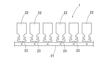
- the copper terminal material with tin plating 1 is to form a plurality of terminals as a whole.
- a plurality of terminal members 22 to be formed as terminals are arranged at intervals in the length direction of the carrier portion 21 in the carrier portion 21 along the length direction.
- the member 22 is connected to the carrier portion 21 via the narrow connecting portion 23.
- Each terminal member 22 is formed into, for example, the shape of the terminal 10 as shown in FIG. 10, and is cut from the connecting portion 23 to complete the terminal 10.
- This terminal 10 shows a female terminal in the example of FIG. 10, and from the tip end, a connecting portion 11 to which a male terminal (not shown) is fitted and a core wire caulking portion to which the exposed core 12a of the electric wire 12 is crimped. 13, the covering caulking part 14 by which the covering part 12b of the electric wire 12 is caulking is integrally formed in this order.
- FIG. 11 shows the end portion structure in which the terminal 10 is crimped to the electric wire 12, and the core caulking portion 13 is in direct contact with the core 12a of the electric wire 12.
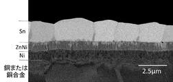
- this copper terminal material 1 with a tin plating is the base layer 3 which consists of nickel or a nickel alloy on the base material 2 which consists of copper or a copper alloy, a zinc nickel alloy layer, as the cross section was typically shown in FIG. 4, the tin layer 5 is laminated in this order, and further, the metal zinc layer 7 is formed on the tin layer 5 under the oxide layer 6 formed on the outermost surface thereof.
- the composition is not particularly limited as long as the substrate 2 is made of copper or a copper alloy.
- this base material 2 is processed into a hoop material of the shape shown in FIG. 3 by press processing etc. (base material processing process), and formation of the foundation layer for forming foundation layer 3 which consists of nickel or a nickel alloy in this hoop material Process, zinc-nickel alloy layer forming process for forming zinc-nickel alloy layer 4, tin plating process for forming tin layer 5 composed of tin or tin alloy, forming tin layer 5 and holding at a predetermined temperature for a fixed time In this order, a diffusion treatment process is carried out to diffuse the zinc of the zinc-nickel alloy layer to the tin layer.
- ⁇ Base material processing process> By subjecting the plate material to processing such as cutting and drilling, a plurality of terminal members 22 are connected to the carrier portion 21 through the connecting portion 23 as shown in FIG. After pressing, the surface is cleaned by degreasing, pickling and the like.
- the foundation layer 3 is formed on the hoop material after the base material processing step.
- the nickel or nickel alloy plating for forming the underlayer 3 is not particularly limited as long as a dense nickel-based film can be obtained, and electricity may be generated using a known watt bath, sulfamic acid bath, citric acid bath or the like. It can be formed by plating.
- Nickel alloy plating includes nickel tungsten (Ni-W) alloy, nickel phosphorus (Ni-P) alloy, nickel cobalt (Ni-Co) alloy, nickel chromium (Ni-Cr) alloy, nickel iron (Ni-Fe) alloy, Nickel zinc (Ni-Zn) alloy, nickel boron (Ni-B) alloy, etc. can be used.
- the underlayer 3 thus formed has a thickness of 0.1 ⁇ m to 5.0 ⁇ m and a nickel content of 80% by mass or more.
- the underlayer 3 has a function of preventing the diffusion of copper from the base material 2 to the zinc-nickel alloy layer 4 and the tin layer 5, and when the thickness is less than 0.1 ⁇ m, the effect of preventing the diffusion of copper is scarce. If it exceeds 0 ⁇ m, cracking tends to occur during press working.
- the thickness of the underlayer 3 is more preferably 0.3 ⁇ m or more and 2.0 ⁇ m or less.
- the nickel content is less than 80% by mass, the effect of preventing copper from diffusing into the zinc-nickel alloy layer 4 or the tin layer 5 is small.
- the nickel content is more preferably 90% by mass or more.
- the zinc-nickel alloy plating for forming the zinc-nickel alloy layer 4 is not particularly limited as long as a dense film can be obtained with a desired composition, and known sulfate bath, chloride salt bath, neutral bath, etc. Can be used. It is important to control the nickel content to a predetermined value in order to prevent tin substitution in the tin plating step.
- the nickel content and crystal structure of the zinc-nickel alloy layer 4 can be adjusted by adjusting the concentration ratio of zinc and nickel in the plating bath.
- the zinc-nickel alloy layer 4 has a thickness of 0.1 ⁇ m to 5.0 ⁇ m, contains zinc and nickel, and also contains tin because it is in contact with the tin layer 5.
- the nickel content of the zinc-nickel alloy layer 4 is 5% by mass or more and 50% by mass or less.
- the thickness of the zinc-nickel alloy layer 4 is less than 0.1 ⁇ m, there is no effect of deteriorating the corrosion potential on the surface, and if it exceeds 5.0 ⁇ m, there is a possibility that cracking may occur at the time of pressing to the terminal 10.
- the thickness of the zinc-nickel alloy layer 4 is more preferably 0.3 ⁇ m or more and 2.0 ⁇ m or less.
- the nickel content of the zinc-nickel alloy layer 4 is less than 5% by mass, a substitution reaction occurs during the later-described tin plating for forming the tin layer 5, and the adhesion of the tin plating (tin layer 5) is significantly reduced. If the content of nickel in the zinc-nickel alloy layer 4 exceeds 50% by mass, there is no effect of deteriorating the surface corrosion potential.
- the nickel content is more preferably 7% by mass or more and 20% by mass or less.
- the zinc-nickel alloy layer 4 be a ⁇ -phase single phase. Since the ⁇ phase has higher corrosion resistance than the ⁇ phase, the substitution reaction at the time of tin plating can be suppressed, and the occurrence of voids at the interface can be remarkably suppressed.
- the discrimination of the ⁇ phase single phase can be confirmed by analyzing the material on which zinc nickel plating is performed by the X-ray diffraction method.
- FIG. 4 (a) shows the mixed state of the ⁇ phase and the ⁇ phase
- FIG. 4 (b) shows the single phase state of the ⁇ phase. Since the peak of the ⁇ phase is close to the copper peak, depending on the plating thickness, the peak may overlap with the copper peak and may not be confirmed.
- the main phases of the zinc-nickel alloy in the case where the nickel concentration is relatively low are the ⁇ phase and the ⁇ phase, and whether or not the phase is the ⁇ single phase can be determined by the presence or absence of the ⁇ phase.
- Tin or tin alloy plating for forming the tin layer 5 can be performed by a known method, for example, an organic acid bath (eg, phenol sulfonic acid bath, alkane sulfonic acid bath or alkanol sulfonic acid bath), fluorous acid It can be electroplated using an acid bath such as a bath, a halogen bath, a sulfuric acid bath or a pyrophosphate bath, or an alkali bath such as a potassium bath or a sodium bath.
- an organic acid bath eg, phenol sulfonic acid bath, alkane sulfonic acid bath or alkanol sulfonic acid bath
- fluorous acid It can be electroplated using an acid bath such as a bath, a halogen bath, a sulfuric acid bath or a pyrophosphate bath, or an alkali bath such as a potassium bath or a sodium bath.
- an acidic organic acid bath or a sulfuric acid bath In view of the plating film formation at high speed, the compactness of the plating film and the ease of zinc diffusion, it is preferable to use an acidic organic acid bath or a sulfuric acid bath.
- the tin layer 5 formed in this step preferably has a thickness of 0.1 ⁇ m or more and 10 ⁇ m or less. If it is too thin, the solder wettability may decrease and the contact resistance may decrease. This causes an increase, and there is a risk that the attachment / detachment resistance at the time of use in a connector or the like may increase.
- This diffusion treatment step is held for 30 minutes or more at a temperature at which the surface temperature of the material is 40 ° C. or more and 160 ° C. or less.
- zinc in the zinc-nickel alloy layer diffuses onto the tin layer to form a thin metallic zinc layer on the surface. Since the diffusion of zinc occurs rapidly, the metallic zinc layer 7 can be formed by exposing it to a temperature of 40 ° C. or more for 30 minutes or more.
- the temperature exceeds 160 ° C.
- tin diffuses to the zinc-nickel side to inhibit the diffusion of zinc
- the zinc-nickel alloy repels molten tin and forms a tin-repelled spot in the tin layer 5 Do not heat to temperatures above 190 ° C.
- the copper terminal material 1 with tin plating manufactured in this manner has a base layer 3 made of nickel or a nickel alloy, a zinc nickel alloy layer 4 and a tin layer 5 laminated in this order on the base material 2 as a whole.
- the oxide layer 6 is thinly formed on the surface of the tin layer 5 and the metallic zinc layer 7 is formed under the oxide layer 6.
- the metal zinc layer 7 is formed to have a zinc concentration of 5 at% or more and 40 at% or less and a thickness of 1 nm or more and 10 nm or less in terms of SiO 2 .
- An oxide layer 6 of zinc or tin is formed on the outermost surface.
- the hoop material is processed into the shape of the terminal 10 shown in FIG. 10 by press processing or the like, and the connection portion 23 is cut to form the terminal 10.
- FIG. 11 shows the end portion structure in which the terminal 10 is crimped to the electric wire 12, and the core caulking portion 13 is in direct contact with the core 12a of the electric wire 12.
- the metal zinc layer 7 is formed under the oxide layer 6 on the outermost surface of the tin layer 5, even if it is crimped to the aluminum core wire 12a, the corrosion potential of the metal zinc Since it is very close to aluminum, the occurrence of electrolytic corrosion can be prevented. In this case, since the plating process is performed in the state of the hoop material in FIG. 3 and the heat treatment is performed, the base material 2 is not exposed also on the end face of the terminal 10, so that an excellent anticorrosion effect can be exhibited.
- the zinc-nickel alloy layer 4 is formed under the tin layer 5 and the zinc diffuses to the surface portion of the tin layer 5, the loss of the metallic zinc layer 7 due to abrasion etc. is suppressed, Layer 7 is maintained at a high concentration. Further, even if all or part of the tin layer 5 disappears due to wear or the like, the zinc nickel alloy layer 4 therebelow has a similar corrosion potential to aluminum, so that the occurrence of electrolytic corrosion can be suppressed.
- the diffusion treatment step is provided after the tin plating step, but the diffusion treatment step is not necessarily required, and may be processed into a terminal without passing through the diffusion treatment step.
- Zinc preferably diffuses rapidly through the above-mentioned diffusion treatment step, but even if it does not go through the diffusion treatment step, metal zinc is obtained from the zinc-nickel alloy layer 4 by leaving it at normal temperature of 10 ° C. or more, for example.
- the metallic zinc layer 7 can be formed on the surface of the tin layer 5 by diffusing into the tin layer 5.
- nickel plating as a base layer was sequentially applied.
- the conditions for each plating were as follows.
- the base layer obtained by these plating treatments and the thickness of the zinc-nickel alloy layer were as shown in Table 1.
- the sample 1 did not form a base layer, and the sample 9 did not implement zinc nickel alloy plating.
- nickel alloy plating nickel-iron plating was performed on sample 2, nickel-phosphorus plating on sample 4, and nickel-tungsten plating on sample 5.
- Nickel sulfamate 300 g / L Nickel chloride: 5 g / L Boric acid: 30 g / L ⁇ Bath temperature: 45 ° C ⁇ Current density: 5A / dm 2
- Sodium sulfate: 140 g / L PH 2.0 ⁇
- the zinc-nickel alloy plating conditions are an example in which the nickel content is 15% by mass, and the nickel content in the zinc-nickel alloy layer is adjusted by adjusting the concentration ratio of zinc to nickel in the plating bath. The content rate shown in
- the nickel content rate is an electron beam microanalyzer (EPMA) manufactured by Nippon Denshi Co., Ltd. JXA-8530F, and a sample on which only zinc nickel alloy plating is deposited under predetermined plating conditions is applied from the surface at an accelerating voltage of 6.5 kV. It observed and measured with the beam diameter of (phi) 30 micrometers.
- the crystal structure of the zinc-nickel layer was confirmed by analyzing the surface by X-ray diffraction before the formation of a tin layer by zinc-nickel plating. Copper was used for the x-ray source.
- samples 5 to 8 were subjected to a diffusion treatment under the temperature conditions shown in Table 1 to obtain samples.
- the thickness and concentration of the metallic zinc layer on the surface of the tin layer were measured for the obtained sample, and the corrosion current, bending workability, presence of interface void, and contact resistance were measured and evaluated.
- ⁇ Thickness and concentration of metallic zinc layer> With regard to the thickness and concentration of the metallic zinc layer, for each sample, an XPS (X-ray Photoelectron Spectroscopy) analyzer manufactured by ULVAC-PHI, Inc .: ULVAC PHI model-5600LS, using XPS while etching the sample surface with argon ions Measured by analysis.
- the analysis conditions are as follows.
- X-ray source Standard MgK ⁇ 350 W Pass energy: 187.85 eV (Survey), 58.70 eV (Narrow) Measurement interval: 0.8 eV / step (Survey), 0.125 eV (Narrow) Photoelectric extraction angle to sample surface: 45 deg Analysis area: about 800 ⁇ m ⁇
- the SiO 2 conversion film thickness was computed from the time required for the measurement using the etching rate of SiO 2 previously measured with the same model.
- XPS has an excellent depth resolution of about 0.5 nm, but the time to be etched by Ar ion beam differs depending on each material, so in order to obtain the numerical value of the film thickness itself, a sample with a known and flat film thickness is procured And the etch rate must be calculated.
- the film thickness is defined by the SiO 2 conversion etching rate, the film thickness can be quantitatively evaluated because it is unique even if the actual film thickness is unknown.
- ⁇ Corrosion current> Regarding the corrosion current, leave the exposed part of diameter 2 mm, place the exposed part facing the exposed part at a distance of 1 mm, and place the pure aluminum wire coated with resin with the resin left with exposed part of diameter 6 mm.
- the corrosion current flowing between the aluminum wire and the sample was measured in 5% by mass saline solution.
- corrosion current was measured after heating the sample at 150 ° C. for 1 hour and before heating using a non-resistance amperometer HA 1510 manufactured by Hokuto Denko Co., Ltd. The average current values for 1000 minutes were compared.
- ⁇ Bendability> With regard to bending workability, test pieces are cut out so that the rolling direction is longitudinal, and using a W bending test jig defined in JIS H 3110, 9.8 ⁇ 10 3 N so as to be in a direction perpendicular to the rolling direction Bending was performed with a load of Thereafter, observation was performed with a stereomicroscope.
- the evaluation of bending workability is a level at which a clear crack is not recognized in the bent portion after the test, which is evaluated as “excellent”, and although a crack is recognized, a level at which exposure of the copper alloy base material is not recognized due to the generated crack. Was evaluated as “good”, and the level at which the copper alloy base material was exposed due to the generated cracks was evaluated as “defective”.
- the contact resistance measurement method is based on JCBA-T323, using a four-terminal contact resistance tester (CRS-113-AU manufactured by Yamazaki Seiki Research Institute, Inc.), with a sliding type (1 mm) and a load of 0.98 N. The contact resistance was measured. The measurement was performed on the plating surface of the flat plate sample.
- ⁇ Interface void> The presence or absence of the interface void due to tin substitution during tin plating was determined by cross-sectioning the sample with a cross section polisher, observing the vicinity of the interface between the nickel-zinc alloy layer and the tin layer with a field emission scanning electron microscope. Those with a clear void exceeding 3 ⁇ m were identified, and those without a clear void were considered nil.
- FIG. 5 is a photomicrograph of a cross section of sample 7. It can be confirmed that an underlayer (nickel layer), a zinc-nickel alloy layer, and a tin layer are formed from the substrate side, but the outermost surface portion of the tin layer Can not be determined.
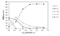
- FIG. 6 is a concentration distribution diagram of each element in the depth direction in the surface portion of the sample 7 by XPS analysis, and it can be seen that a metallic zinc layer having a high zinc concentration is present near the surface.
- FIG. 7 is a chemical state analysis diagram of the sample 7 in the depth direction. From the chemical shift of the binding energy, it can be judged that the oxide is mainly at a depth of 1.25 nm from the outermost surface, and the metal zinc is mainly at 2.5 nm and thereafter.
- samples 4 to 8 in which an underlayer having a thickness of 0.1 ⁇ m to 5.0 ⁇ m and a nickel content of 80% by mass or more was formed between the substrate and the zinc-nickel alloy layer have the underlayer.
- Sample 9 of the Comparative Example had a high corrosion current because it did not form a zinc-nickel alloy layer. Further, in the sample 10, the thickness of the zinc-nickel alloy layer exceeds 5.0 ⁇ m, fatal fracture of the plated surface occurs, and the bending workability is inferior. In Sample 11, the nickel content of the zinc-nickel alloy layer was less than 5% by mass, so interface voids were generated, the adhesion of the tin layer was inferior, and cracks were generated during bending. In sample 12, the nickel content of the zinc-nickel alloy layer exceeded 50% by mass, and the diffusion of zinc was insufficient, resulting in high corrosion current. Sample 13 had a zinc-nickel alloy layer as thin as 0.07 ⁇ m, so the zinc diffusion was insufficient and the corrosion current was high.
- FIG. 8 shows the measurement results of the corrosion current of Samples 7 and 9.
- the value is shown also for the terminal material of oxygen free copper (C1020) which is not plated.
- the corrosion current is larger at a positive value, the aluminum wire is subject to galvanic corrosion, and as shown in FIG. 8, it can be seen that the sample 7 of the example has a smaller corrosion current and can suppress the occurrence of electrolytic corrosion.
- FIG. 9 shows the cross-sectional observation result of the sample 11, and it can be seen that the zinc-nickel alloy layer is subjected to a tin substitution reaction at the time of tin plating, a clear void is formed, and the bonding interface is rough.
Abstract
Description
の水酸化酸化物を含んだものとされている。そして、このSn3O2(OH)2の水酸化酸
化物を含む導電性皮膜層により、高温環境下での耐久性が向上し、長期間にわたって低い接触抵抗を維持することができると記載されている。
本実施形態の製造方法により形成される錫めっき付き銅端子材について説明しておくと、この錫めっき付き銅端子材1は、図3に全体を示したように、複数の端子を成形するための帯板状のフープ材であり、長さ方向に沿うキャリア部21に、端子として成形すべき複数の端子用部材22がキャリア部21の長さ方向に間隔をおいて配置され、各端子用部材22が細幅の連結部23を介してキャリア部21に連結されている。各端子用部材22は例えば図10に示すような端子10の形状に成形され、連結部23から切断されることにより、端子10として完成する。
基材2は、銅又は銅合金からなるものであれば、特に、その組成が限定されるものではない。
この板材に裁断、穴明け等の加工を施すことにより、図3に示すような、キャリア部21に複数の端子用部材22を連結部23を介して連結されてなるフープ材に成形する。プレス加工後、脱脂、酸洗等の処理をすることによって表面を清浄にする。
基材加工工程後のフープ材に下地層3を形成する。
この下地層3を形成するためのニッケル又はニッケル合金めっきは緻密なニッケル主体の膜が得られるものであれば特に限定されず、公知のワット浴やスルファミン酸浴、クエン酸浴などを用いて電気めっきにより形成することができる。ニッケル合金めっきとしてはニッケルタングステン(Ni-W)合金、ニッケルリン(Ni-P)合金、ニッケルコバルト(Ni-Co)合金、ニッケルクロム(Ni-Cr)合金、ニッケル鉄(Ni-Fe)合金、ニッケル亜鉛(Ni-Zn)合金、ニッケルボロン(Ni-B)合金などを利用することができる。
亜鉛ニッケル合金層4を形成するための亜鉛ニッケル合金めっきは、緻密な膜を所望の組成で得られるものであれば特に限定されず、公知の硫酸塩浴や塩化物塩浴、中性浴などを用いることができる。錫めっき工程での錫置換を防ぐためにニッケル含有率を所定の値に制御することが肝要である。
錫層5を形成するための錫又は錫合金めっきは、公知の方法により行うことができるが、例えば有機酸浴(例えばフェノールスルホン酸浴、アルカンスルホン酸浴又はアルカノールスルホン酸浴)、硼フッ酸浴、ハロゲン浴、硫酸浴、ピロリン酸浴等の酸性浴、或いはカリウム浴やナトリウム浴等のアルカリ浴を用いて電気めっきすることができる。
この拡散処理工程は、素材の表面温度が40℃以上160℃以下となる温度で30分以上保持する。この拡散処理により、亜鉛ニッケル合金層中の亜鉛が錫層上に拡散し、表面に薄く金属亜鉛層を形成する。亜鉛の拡散は速やかに起こるため、40℃以上の温度に30分以上晒すことで金属亜鉛層7を形成することができる。ただし、160℃を超えると逆に錫が亜鉛ニッケル側に拡散し亜鉛の拡散を阻害する、さらに190℃を超えると亜鉛ニッケル合金は溶融錫をはじき、錫層5に錫はじき箇所を形成するため、190℃を超える温度には加熱しない。
・めっき浴組成
スルファミン酸ニッケル:300g/L
塩化ニッケル:5g/L
ホウ酸:30g/L
・浴温:45℃
・電流密度:5A/dm2
・めっき浴組成
硫酸亜鉛七水和物:75g/L
硫酸ニッケル六水和物:180g/L
硫酸ナトリウム:140g/L
・pH=2.0
・浴温:45℃
・電流密度:5A/dm2
この亜鉛ニッケル合金めっき条件は、ニッケル含有率が15質量%となる例であり、亜鉛ニッケル合金層中のニッケル含有率は、めっき浴中の亜鉛とニッケルの濃度比を調整することにより、表1に示す含有率とした。
・めっき浴組成
メタンスルホン酸錫:200g/L
メタンスルホン酸:100g/L
光沢剤
・浴温:25℃
・電流密度:5A/dm2
亜鉛ニッケル層の結晶構造については、亜鉛ニッケルめっきを施して錫層を形成する前に、表面をX線回折法により解析して確認した。銅をX線源に使用した。

金属亜鉛層の厚みと濃度については、各試料について、アルバック・ファイ株式会社製のXPS(X-ray Photoelectron Spectroscopy)分析装置:ULVAC PHI model-5600LSを用い、試料表面をアルゴンイオンでエッチングしながらXPS分析により測定した。その分析条件は以下の通りである。
パスエネルギー:187.85eV(Survey)、58.70eV(Narrow)
測定間隔:0.8eV/step(Survey)、0.125eV(Narrow)
試料面に対する光電子取り出し角:45deg
分析エリア:約800μmφ
腐食電流については、直径2mmの露出部を残し樹脂で被覆した純アルミニウム線と直径6mmの露出部を残し樹脂で被覆した試料とを距離1mmにて露出部を対向させて設置し、23℃の5質量%食塩水中でアルミニウム線と試料との間に流れる腐食電流を測定した。腐食電流測定には北斗電工株式会社製無抵抗電流計HA1510を用い、試料を150℃で1時間加熱した後と加熱前との腐食電流を比較した。1000分間の平均電流値を比較した。
曲げ加工性については、試験片を圧延方向が長手となるように切出し、JISH3110に規定されるW曲げ試験治具を用い、圧延方向に対して直角方向となるように9.8×10³Nの荷重で曲げ加工を施した。その後、実体顕微鏡にて観察を行った。曲げ加工性評価は、試験後の曲げ加工部に明確なクラックが認められないレベルを「優」と評価し、クラックは認められるが、発生したクラックにより銅合金母材の露出が認められないレベルを「良」と評価し、発生したクラックにより銅合金母材が露出しているレベルを「不良」と評価した。
接触抵抗の測定方法はJCBA-T323に準拠し、4端子接触抵抗試験機(株式会社山崎精機研究所製:CRS-113-AU)を用い、摺動式(1mm)で荷重0.98N時の接触抵抗を測定した。平板試料のめっき表面に対して測定を実施した。
錫めっき時の錫置換による界面ボイドの有無は、サンプルをクロスセクションポリッシャーにて断面加工し、ニッケル亜鉛合金層と錫層との界面付近を電解放射型走査電子顕微鏡にて観察し、直径0.3μmを超える明確なボイドが認められたものを有とし、明確なボイドがないものを無とした。

2 基材
3 下地層
4 亜鉛ニッケル合金層
5 錫層
6 酸化物層
7 金属亜鉛層
10 端子
11 接続部
12 電線
12a 心線
12b 被覆部
13 心線かしめ部
14 被覆かしめ部
Claims (5)
- 銅又は銅合金からなる基材の上にニッケル含有率が5質量%以上50質量%以下の亜鉛ニッケル合金層を0.1μm以上5.0μm以下の厚さで形成する亜鉛ニッケル合金層形成工程と、前記亜鉛ニッケル合金層の上に錫めっきを施して錫層を形成する錫めっき工程と、を有することを特徴とする錫めっき付き銅端子材の製造方法。
- 前記亜鉛ニッケル合金層の結晶構造がγ相単相であることを特徴とする請求項1記載の錫めっき付き銅端子材の製造方法。
- 前記亜鉛ニッケル合金層形成工程の前に、前記基材の表面にニッケル含有率が80質量%以上のニッケル又はニッケル合金からなる下地層を0.1μm以上5.0μm以下の厚さで形成する下地層形成工程を有することを特徴とする請求項1又は2記載の錫めっき付き銅端子材の製造方法。
- 前記錫めっき工程の後に40℃以上160℃以下に30分以上保持して、前記亜鉛ニッケル合金層の亜鉛を前記錫層に拡散させる拡散処理工程を有することを特徴とする請求項1記載の錫めっき付き銅端子材の製造方法。
- 前記基材は、予めプレス加工によりフープ材に形成されており、前記フープ材は、帯板状に形成されるとともに、その長さ方向に沿うキャリア部に、端子に成形されるべき複数の端子用部材が前記キャリア部の長さ方向に間隔をおいて連結されていることを特徴とする請求項1記載の錫めっき付き銅端子材の製造方法。
Priority Applications (6)
| Application Number | Priority Date | Filing Date | Title |
|---|---|---|---|
| US15/778,336 US10301737B2 (en) | 2015-12-15 | 2016-12-14 | Method of manufacturing tin-plated copper terminal material |
| KR1020187018099A KR102537040B1 (ko) | 2015-12-15 | 2016-12-14 | 주석 도금이 형성된 구리 단자재의 제조 방법 |
| MX2018006603A MX2018006603A (es) | 2015-12-15 | 2016-12-14 | Metodo para fabricar material de terminal de cobre bañado en estaño. |
| MYPI2018702110A MY190168A (en) | 2015-12-15 | 2016-12-14 | Method of manufacturing tin-plated copper terminal material |
| CN201680073372.4A CN108368627B (zh) | 2015-12-15 | 2016-12-14 | 镀锡铜端子材的制造方法 |
| EP16875659.1A EP3392382A4 (en) | 2015-12-15 | 2016-12-14 | METHOD FOR MANUFACTURING STAINLESS COPPER TERMINAL MATERIAL |
Applications Claiming Priority (4)
| Application Number | Priority Date | Filing Date | Title |
|---|---|---|---|
| JP2015244311 | 2015-12-15 | ||
| JP2015-244311 | 2015-12-15 | ||
| JP2016-150740 | 2016-07-29 | ||
| JP2016150740A JP6226037B2 (ja) | 2015-12-15 | 2016-07-29 | 錫めっき付き銅端子材の製造方法 |
Publications (1)
| Publication Number | Publication Date |
|---|---|
| WO2017104682A1 true WO2017104682A1 (ja) | 2017-06-22 |
Family
ID=59056761
Family Applications (1)
| Application Number | Title | Priority Date | Filing Date |
|---|---|---|---|
| PCT/JP2016/087137 WO2017104682A1 (ja) | 2015-12-15 | 2016-12-14 | 錫めっき付き銅端子材の製造方法 |
Country Status (2)
| Country | Link |
|---|---|
| MY (1) | MY190168A (ja) |
| WO (1) | WO2017104682A1 (ja) |
Cited By (2)
| Publication number | Priority date | Publication date | Assignee | Title |
|---|---|---|---|---|
| CN110277192A (zh) * | 2018-03-14 | 2019-09-24 | 日立金属株式会社 | 镀锡铜线及其制造方法以及绝缘电线、电缆 |
| CN110997984A (zh) * | 2017-07-28 | 2020-04-10 | 三菱综合材料株式会社 | 镀锡铜端子材、端子及电线终端部结构 |
Citations (7)
| Publication number | Priority date | Publication date | Assignee | Title |
|---|---|---|---|---|
| JPH0841681A (ja) * | 1994-07-25 | 1996-02-13 | Kobe Steel Ltd | Ni−Zn系合金めっき鋼板の製法 |
| JPH11193494A (ja) * | 1997-12-26 | 1999-07-21 | Kobe Steel Ltd | かん合型接続端子用めっき材及びかん合型接続端子 |
| JP2000144482A (ja) * | 1998-09-11 | 2000-05-26 | Nippon Mining & Metals Co Ltd | 金属材料 |
| JP2000169996A (ja) * | 1998-09-28 | 2000-06-20 | Nippon Mining & Metals Co Ltd | 金属材料 |
| JP2003328157A (ja) * | 2002-05-02 | 2003-11-19 | Furukawa Electric Co Ltd:The | めっき材料とその製造方法、それを用いた電気・電子部品 |
| WO2013161125A1 (ja) * | 2012-04-26 | 2013-10-31 | 株式会社オートネットワーク技術研究所 | コネクタ用めっき端子 |
| JP2014164927A (ja) * | 2013-02-23 | 2014-09-08 | Furukawa Electric Co Ltd:The | 圧着端子および接続構造体 |
-
2016
- 2016-12-14 WO PCT/JP2016/087137 patent/WO2017104682A1/ja active Application Filing
- 2016-12-14 MY MYPI2018702110A patent/MY190168A/en unknown
Patent Citations (7)
| Publication number | Priority date | Publication date | Assignee | Title |
|---|---|---|---|---|
| JPH0841681A (ja) * | 1994-07-25 | 1996-02-13 | Kobe Steel Ltd | Ni−Zn系合金めっき鋼板の製法 |
| JPH11193494A (ja) * | 1997-12-26 | 1999-07-21 | Kobe Steel Ltd | かん合型接続端子用めっき材及びかん合型接続端子 |
| JP2000144482A (ja) * | 1998-09-11 | 2000-05-26 | Nippon Mining & Metals Co Ltd | 金属材料 |
| JP2000169996A (ja) * | 1998-09-28 | 2000-06-20 | Nippon Mining & Metals Co Ltd | 金属材料 |
| JP2003328157A (ja) * | 2002-05-02 | 2003-11-19 | Furukawa Electric Co Ltd:The | めっき材料とその製造方法、それを用いた電気・電子部品 |
| WO2013161125A1 (ja) * | 2012-04-26 | 2013-10-31 | 株式会社オートネットワーク技術研究所 | コネクタ用めっき端子 |
| JP2014164927A (ja) * | 2013-02-23 | 2014-09-08 | Furukawa Electric Co Ltd:The | 圧着端子および接続構造体 |
Cited By (5)
| Publication number | Priority date | Publication date | Assignee | Title |
|---|---|---|---|---|
| CN110997984A (zh) * | 2017-07-28 | 2020-04-10 | 三菱综合材料株式会社 | 镀锡铜端子材、端子及电线终端部结构 |
| EP3660190A4 (en) * | 2017-07-28 | 2021-04-28 | Mitsubishi Materials Corporation | TINNED COPPER TERMINAL MATERIAL, TERMINAL, AND CONDUCTIVE WIRE END STRUCTURE |
| CN110997984B (zh) * | 2017-07-28 | 2022-04-26 | 三菱综合材料株式会社 | 镀锡铜端子材、端子及电线终端部结构 |
| CN110277192A (zh) * | 2018-03-14 | 2019-09-24 | 日立金属株式会社 | 镀锡铜线及其制造方法以及绝缘电线、电缆 |
| CN110277192B (zh) * | 2018-03-14 | 2022-02-22 | 日立金属株式会社 | 镀锡铜线及其制造方法以及绝缘电线、电缆 |
Also Published As
| Publication number | Publication date |
|---|---|
| MY190168A (en) | 2022-03-31 |
Similar Documents
| Publication | Publication Date | Title |
|---|---|---|
| JP6304447B2 (ja) | 錫めっき付銅端子材及び端子並びに電線端末部構造 | |
| KR102355341B1 (ko) | 주석 도금 형성 구리 단자재 및 단자 그리고 전선 단말부 구조 | |
| KR102537040B1 (ko) | 주석 도금이 형성된 구리 단자재의 제조 방법 | |
| JP6812852B2 (ja) | 防食端子材及び防食端子並びに電線端末部構造 | |
| CN110214203B (zh) | 连接器用端子材及端子以及电线末端部结构 | |
| JP6620897B2 (ja) | 錫めっき付銅端子材及び端子並びに電線端末部構造 | |
| KR102531227B1 (ko) | 방식 단자재 및 방식 단자 그리고 전선 단말부 구조 | |
| WO2017104682A1 (ja) | 錫めっき付き銅端子材の製造方法 | |
| WO2018212174A1 (ja) | 錫めっき付銅端子材及び端子並びに電線端末部構造 | |
| JP6743556B2 (ja) | 錫めっき付銅端子材の製造方法 |
Legal Events
| Date | Code | Title | Description |
|---|---|---|---|
| 121 | Ep: the epo has been informed by wipo that ep was designated in this application |
Ref document number: 16875659 Country of ref document: EP Kind code of ref document: A1 |
|
| WWE | Wipo information: entry into national phase |
Ref document number: MX/A/2018/006603 Country of ref document: MX |
|
| NENP | Non-entry into the national phase |
Ref country code: DE |
|
| ENP | Entry into the national phase |
Ref document number: 20187018099 Country of ref document: KR Kind code of ref document: A |
|
| WWE | Wipo information: entry into national phase |
Ref document number: 2016875659 Country of ref document: EP |
|
| ENP | Entry into the national phase |
Ref document number: 2016875659 Country of ref document: EP Effective date: 20180716 |