WO2017104453A1 - 接合体の製造方法 - Google Patents
接合体の製造方法 Download PDFInfo
- Publication number
- WO2017104453A1 WO2017104453A1 PCT/JP2016/085977 JP2016085977W WO2017104453A1 WO 2017104453 A1 WO2017104453 A1 WO 2017104453A1 JP 2016085977 W JP2016085977 W JP 2016085977W WO 2017104453 A1 WO2017104453 A1 WO 2017104453A1
- Authority
- WO
- WIPO (PCT)
- Prior art keywords
- bonding layer
- joined body
- bonding
- manufacturing
- optical element
- Prior art date
- Legal status (The legal status is an assumption and is not a legal conclusion. Google has not performed a legal analysis and makes no representation as to the accuracy of the status listed.)
- Ceased
Links
Images





Classifications
-
- B—PERFORMING OPERATIONS; TRANSPORTING
- B29—WORKING OF PLASTICS; WORKING OF SUBSTANCES IN A PLASTIC STATE IN GENERAL
- B29C—SHAPING OR JOINING OF PLASTICS; SHAPING OF MATERIAL IN A PLASTIC STATE, NOT OTHERWISE PROVIDED FOR; AFTER-TREATMENT OF THE SHAPED PRODUCTS, e.g. REPAIRING
- B29C65/00—Joining or sealing of preformed parts, e.g. welding of plastics materials; Apparatus therefor
Definitions
- the present invention relates to a method for manufacturing a joined body including a plurality of members.
- a joint provided on a pair of objects to be joined is cleaned with energy waves in vacuum (surface activation treatment), and then joined at room temperature in the atmosphere (specifically, from room temperature to A method of joining at 180 ° C. or lower is known (for example, see Patent Document 1).
- a metal such as copper or a semiconductor can be cited as an object to be joined, and a surface-activatable metal (specifically, gold, aluminum, copper, etc.) or a material other than a metal can be cited as a joint. Yes.
- a metal having a relatively soft hardness such as gold or copper at the bonding interface, the softness of the metal applied to the bonding interface serves as a buffer material, and the bonding interface is smoothed while bonding. is doing.
- a method of joining a first substrate made of a transparent material containing silicon dioxide and another substrate at room temperature (specifically, joining at 20 ° C. ⁇ 15 ° C.).
- a bonding layer provided on a part of a first substrate and a bonding layer provided on a part of another substrate are adhered to each other to bond these bonding layers.
- the bonding layer of Patent Document 2 is formed of a metal material (specifically, gold, platinum, an alloy containing these metals, or the like) containing a metal that has a positive free energy of formation of oxide at room temperature. Further, the bonding disclosed in Patent Document 2 can be performed in the air, in a reduced pressure environment, or in an atmosphere of atmospheric pressure or higher.
- the member to be joined is formed of a metal or a material containing silicon dioxide, the amount that can smooth the joining surface at the time of joining is about several tens of nm. If unevenness exists on the joint surface beyond the range, these members can hardly be joined.
- An object of the present invention is to provide a method of manufacturing a joined body in which a plurality of members are joined in a good state.
- a method for manufacturing a joined body according to the present invention includes a joining layer using an inorganic substance at least on the joining side portion of the first member among the first member and the second member formed of the polymer material.
- the surface of the bonding layer is activated, and the first member and the second member are bonded via the bonding layer in the atmosphere with the surface of the bonding layer being activated.
- the second member is formed of a flexible polymer material, even if the surface shape of each member has a swell of about several tens of micrometers, the joining layer is smooth. And the first and second members can be firmly joined. Moreover, since the second member has flexibility, the joining can be achieved regardless of the thicknesses of the first and second members. In addition, since the bonding is performed in the air, it is possible to save time and effort such as evacuation. In addition, since the bonding layer is formed of an inorganic material, shrinkage or the like does not occur as compared with the case of bonding with an adhesive, and positional displacement occurs between the first and second members due to curing or environmental variation. Can be prevented.
- FIG. 1A is a cross-sectional view of a light source unit including the joined body of the first embodiment
- FIG. 1B is a plan view of the joined body shown in FIG. 1A
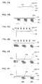
- 2A to 2F are diagrams for explaining a method of manufacturing a joined body.
- 3A to 3F are diagrams for explaining a manufacturing method according to a modification.
- 4A is a perspective view of a light source unit including the joined body of the second embodiment
- FIG. 4B is an exploded view of the optical unit of FIG. 4A.
- 5A is a cross-sectional view of the joined body shown in FIG. 3A, taken along the line AA.
- FIGS. 5B and 5C are diagrams illustrating a modification of the light source unit of FIG. 5A.
- FIG. 9A is a cross-sectional view of a light source unit including a joined body according to the fourth embodiment
- FIGS. 9B and 9C are diagrams illustrating a modification of the light source unit of FIG. 9A.
- 10A to 10D are views for explaining a method of manufacturing the joined body according to the fifth embodiment.
- the joined body 100 is used for optical applications, and includes an optical element 10 as a second member and a substrate 20 as a first member.
- the optical element 10 and the substrate 20 are stacked and bonded in the Z-axis direction perpendicular to the XY plane from which the substrate 20 extends.
- the joined body 100 can be used as the light source unit 200 by providing the light emitting element 22 on the substrate 20, for example.
- the optical element 10 is a light-transmitting member that can transmit light in the wavelength range to be used.
- the optical element 10 is a transparent member.
- the optical element 10 is made of a polymer material.
- a polymer material for example, a thermoplastic resin, an energy curable resin, a two-component curable resin, or the like is used.
- COP cycloolefin polymer
- PMMA acrylic
- PC polycarbonate
- the energy curable resin for example, an ultraviolet curable resin, a thermosetting resin, or the like is used.
- the two-component curable resin for example, epoxy, silicone or the like is used.
- the optical element 10 has a rectangular outline when viewed from the optical axis OA direction.
- the optical element 10 includes a lens element 10a and a support portion 10b that supports the lens element 10a from the periphery.
- the lens element 10a is a biconvex aspheric lens, for example, and has a first optical surface 11a and a second optical surface 11b.
- the support portion 10b has a flat plate portion 12a and a pair of leg portions 12b extending from the flat plate portion 12a in parallel to the optical axis OA.
- the leg portion 12b is formed corresponding to a portion where the optical element 10 and the substrate 20 are to be joined.
- the leg portion 12b has a quadrangular prism shape having a pair of elongated horizontal cross sections parallel to each other.
- the arrangement and shape of the leg portions 12b can be changed as appropriate as long as the flat plate portion 12a of the support portion 10b can be kept parallel and stable to the substrate 20.
- the optical element 10 and the substrate 20 are bonded with their surfaces activated, and the leg portion 12b of the optical element 10 and the substrate 20 are firmly bonded via the bonding layer 30. ing.
- the optical element 10 is used as a condensing lens, for example.
- the substrate 20 is a transparent and light-transmitting plate-like member, and is a glass substrate formed of inorganic glass.
- the optical element 10 is bonded to the first surface 20 a on the front side of the substrate 20. Further, as already described, in the illustrated example, the light emitting element 22 is provided on the second surface 20 b on the back side of the substrate 20. The center of the light emitting element 22 is disposed on the optical axis OA of the optical element 10.
- the light emitting element 22 for example, an organic EL or LED element is used.
- a bonding layer 30 is provided between the optical element 10 and the substrate 20. That is, the molded optical element (second member) 10 is bonded to the substrate (first member) 20 via the bonding layer 30.
- gold, copper, silver alloy, or the like is used for the bonding layer 30. In the case of gold, the activation stability is high even in the air, and a stable and strong bond is easily obtained. In the case of copper and silver alloys, the cost can be reduced more than gold.
- the thickness of the bonding layer 30 in the direction parallel to the optical axis OA is preferably 1 nm or more, and more preferably 10 nm or more.
- the bonding layer 30 may be locally provided at a position corresponding to the leg portion 12 b of the optical element 10 or may be provided on the entire first surface 20 a of the substrate 20.
- the bonding layer 30 is formed on the bonding side portion G1 of the optical element 10 and the bonding side portion G2 of the substrate 20, and these are bonded, the bonding layer 30 on the optical element 10 side and the bonding on the substrate 20 side are bonded.
- the layer 30 is bonded to each other by a strong chemical bond such as a metal bond. As described above, in the bonded body 100, the optical element 10 and the substrate 20 are in a strong bonded state via the bonding layer 30, and thus have high environmental resistance.
- the bonding layer 30 does not have a film shape but an island shape, but the optical element 10 and the substrate 20 can be bonded to each other although the bonding force is weaker than in the case of the film shape.
- a metal or the like enters the bonding side portions G 1, G 2 of each member 10, 20 to form a mixed layer, or each member 10, 20 and the bonding layer 30 Are chemically bonded.
- an adhesive layer may be provided between the members 10 and 20 and the bonding layer 30.
- a silanol-containing adhesive or the like, specifically a silane coupling agent or the like may be interposed at the bonding interface.
- the bonding layer 30 may not be provided on the side of the optical element 10 that is the second member.
- the optical element 10 as the second member is molded.
- injection molding, mold molding, or the like is used.
- the bonding layer 30 is formed on the end surface 12c of the leg portion 12b of the optical element 10 (that is, the bonding side portion G1 of the optical element 10).
- the bonding layer 30 is formed by vapor deposition, sputtering, or the like.
- the bonding layer 30 is formed on the first surface 20a of the substrate 20 (that is, the bonding side portion G2 of the substrate 20).
- the bonding layer 30 is formed by vapor deposition, sputtering, or the like. Note that the bonding layer 30 on the optical element 10 side and the bonding layer 30 on the substrate 20 side may be formed of different materials or may be formed of the same material. Further, when the substrate 20 that is the first member and the bonding layer 30 are made of the same material, the bonding layer 30 may not be additionally provided.
- an activation treatment for activating the surface is performed on both the bonding layer 30 on the optical element 10 and the bonding layer 30 on the substrate 20.
- the activation treatment corona treatment, plasma treatment, ozone treatment, ultraviolet (UV) treatment, or the like is performed.
- the activation process is performed partially or entirely on the end surface 12 c of the leg portion 12 b of the optical element 10 and the first surface 20 a of the substrate 20.
- the surface SS1 and SS2 of the bonding layer 30 on the optical element 10 side and the surface SS1 and SS2 of the bonding layer 30 on the substrate 20 side are respectively activated, and a surface state in which both can be firmly bonded can be obtained.
- the activation treatment can be preferably performed at room temperature in the atmosphere.
- normal temperature means 20 ° C. ⁇ 15 ° C.
- the light emitting element 22 is not only integrally formed on the second surface 20b side of the substrate 20 but is attached in a subsequent process. In this case, it is preferable to attach the light emitting element 22 to the substrate 20 before performing the above processing.
- the optical element 10 and the substrate 20 are positioned. Specifically, as shown in FIG. 2E, the bonding layer 30 on the optical element 10 side and the bonding layer 30 on the substrate 20 side face each other, and the surface of the bonding layer 30 is activated while maintaining the optical state.
- the element 10 and the substrate 20 are arranged at a bonding position with a gap therebetween.
- the distance between the optical element 10 and the substrate 20 at the time of positioning is preferably 100 nm or more. In positioning, either one of the optical element 10 and the substrate 20 may be moved, or both may be moved relatively.
- the optical element 10 and the substrate 20 are provided with positioning marks, for example, and positioning is performed by matching the mark positions. In addition, if an abutting portion serving as a positioning reference is provided on the optical element 10 and the substrate 20, positioning can be performed by abutting the abutting portion.
- the optical element 10 and the substrate 20 are brought into contact with each other and bonded so as to sandwich the bonding layer 30 with the surface activated.
- This joining is preferably performed at room temperature in the atmosphere.
- the bonding layer 30 on the optical element 10 side and the bonding layer 30 on the substrate 20 side are firmly bonded to each other at the bonding interface in the activated state.
- the bonding layer 30 When the bonding layer 30 is provided at a position corresponding to the plurality of leg portions 12b of the optical element 10, the optical element 10 is bonded to the substrate 20 at a plurality of positions with a space SP. These leg portions 12b are bonded together to the substrate 20.
- bonding is performed by bringing the optical element 10 and the substrate 20 into contact with each other, and the surface of the bonding layer 30 is brought into an activated state so that it can be bonded with close contact with a predetermined pressure or more. You may make it not join only by contact
- the surface of the bonding layer 30 is arranged at the bonding position in a state where the optical element 10 and the substrate 20 are in contact with each other while maintaining an activated state in which bonding can be performed with close contact with a predetermined pressure or more. Thereafter, the optical element 10 and the substrate 20 are bonded to each other by pressurizing at a predetermined pressure or higher.
- 3A to 3F are diagrams for explaining a modification of the manufacturing method shown in FIGS. 2A to 2F.
- LaF 2 , AlN, ITO (tin-doped indium oxide) or the like is used as the bonding layer 30, any of these is formed on the substrate 20 made of a glass plate or the like as the first member, and an activation process is performed.
- a flat plate 112b as a second member made of a polymer material whose surface 112c is activated without providing the bonding layer 30 is prepared, and the substrate 20 and the flat plate 112b are arranged so that the activation surfaces face each other. By contacting and pressing, the joined body 100 joined with a strong joining force can be obtained regardless of the undulation of the polymer material.
- the flat plate 112b may be a part of the optical element 10 shown in FIG. 1A (for example, the leg portion 12b).
- a belt-shaped glass plate corresponding to the first member and a belt-shaped resin flat plate corresponding to the second member are prepared.
- a gold to be a bonding layer was formed into a thickness of 20 nm using a sputtering apparatus.
- a chromium film having a thickness of 10 nm was formed on the glass plate using a sputtering apparatus prior to gold film formation.
- the plasma generator is released to the atmosphere, the bonding positions are aligned within 30 minutes, and the activated surfaces of the resin flat plate and glass plate are brought into contact with each other so as to form a cross when viewed from the overlapping direction. I let you. And joining was completed by pressurizing for 10 seconds with the pressing force of 100 N simultaneously with contact
- the bonded body thus obtained is arranged so that the glass plate faces upward, and further, a getter-shaped pressure jig is arranged so as to straddle the glass plate, and both ends of the resin flat plate are sandwiched through the pressure jig.
- a push gauge SIMP FGP-50
- the surface of the glass plate on which LaF 2 was formed was turned up.
- activation treatment was performed on a glass plate and a resin flat plate under the conditions of a degree of vacuum of 0.3 Mpa, a flow rate of plasma gas N 2 of 100 ml / min, and a plasma output of 200 W.
- the plasma generator is released to the atmosphere, the bonding positions are aligned within 30 minutes, and the activated surfaces of the resin flat plate and glass plate are brought into contact with each other so as to form a cross when viewed from the overlapping direction. I let you. And joining was completed by pressurizing for 10 seconds with the pressing force of 100 N simultaneously with contact
- the bonded body thus obtained is placed so that the glass plate is on top, and further, a getter-shaped pressure jig is placed across the glass plate, and the resin flat plate is pushed through this pressure jig.
- pressure with (SIMP FGP-50) By applying pressure with (SIMP FGP-50), a force was applied in the direction in which the two peeled off. As a result, even when a tensile force of up to 20 MPa was applied, the two could not be peeled off, and the joined body broke when a tensile force exceeding 20 MPa was applied.
- the optical element 10 as the second member is formed of a flexible polymer material
- the members 10 and 20 are about several tens of ⁇ m. Even if it has undulations, it can be smoothed by the bonding layer 30 by pressurization during contact, and the substrate 20 as the first member and the optical element 10 as the second member can be firmly bonded. Further, since the optical element 10 has flexibility, bonding can be achieved regardless of the thickness of the optical element 10 and the substrate 20. In addition, since the bonding is performed in the air, it is possible to save time and effort such as evacuation.
- the bonding layer 30 is formed of an inorganic material, shrinkage or the like does not occur as compared with the case of bonding with an adhesive, and positional displacement occurs between the optical element 10 and the substrate 20 due to curing or environmental variation. Can be prevented.
- different materials can be bonded at a use environment temperature, for example, room temperature, stress and peeling due to a difference in linear expansion during use can be suppressed.
- the optical element 10 and the substrate 20 are transparent and light transmissive members, they are bonded via the bonding layer 30 whose surface is activated, so that the bonding state is good. That is, the optical element 10 and the substrate 20 can be joined regardless of the color, and both are not limited to transparent members, and for example, a black member may be used.
- the bonding performed through the bonding layer 30 whose surface is activated is suitable for bonding of a member having light transmittance, dislikes distortion, and having environmental resistance, particularly those having high importance with respect to displacement. Therefore, even in the joined body 100 in which the optical element 10 and the substrate 20 are combined, a good joined state can be achieved and maintained.
- a plurality of optical elements 10 that are second members are bonded to a substrate 20 that is one first member via a bonding layer 30.
- a light shield 40 is provided between the substrate 20 and the optical element 10.
- the light source unit 200 including the joined body 100 is used for a print head or the like, for example.
- the optical element 10 has a rectangular outline when viewed from the direction of the optical axis OA.
- the optical element 10 includes a plurality of lens elements 10a and a support portion 10b that supports the plurality of lens elements 10a from the periphery.
- the lens elements 10a are provided in an array.
- the support portion 10b has leg portions 12b extending in a direction perpendicular to the flat plate portion 12a from two opposing sides of the flat plate portion 12a having a flat plate-like outer shape.
- a plurality of light emitting elements 22 are provided in an array at positions corresponding to the lens elements 10 a of the optical element 10.
- the light emitting element 22 can be provided not only on the second surface 20b side of the substrate 20 but also on the first surface 20a side of the front.
- the light shield 40 is a flat plate member that shields unnecessary light from the light emitting element 22.
- the light shielding body 40 for example, a glass or resin substrate containing light-absorbing particles such as black, a metal substrate painted black, or the like is used.
- An opening 40 a is formed in the light shielding body 40 at a position corresponding to the lens element 10 a of the optical element 10.
- the light shield 40 is bonded to the substrate 20 side.
- the light shielding body 40 may be bonded with an adhesive, but may be bonded by using a bonding layer whose surface is activated, similar to the bonding between the optical element 10 and the substrate 20, depending on the combination of materials. .
- the material of the light blocking body 40 is made of resin, the light shielding body 40 can be bonded via the bonding layer 130 whose surface is activated.
- the same number of light shielding bodies 40 as the number of pieces of the optical element 10 are arranged, but if optically acceptable, a smaller number than the optical element 10 may be arranged, or 1 as a whole.
- Two plate-like members may be used.
- a plurality of optical elements 10 may be bonded at a time in a state where all of the plurality of optical elements 10 are arranged on the first surface 20a of the substrate 20, or a plurality of optical elements 10 arranged in units of one or several. You may join in divided times.
- the bonding with the surface activated can be performed in a relatively short time, even if a plurality of optical elements 10 are bonded at once or divided into a plurality of times, a comparison is made. It can be joined in a short time and productivity is good.
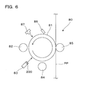
- the light source unit 200 including the joined body 100 is incorporated in an image forming unit 80 built in an electrophotographic printer as an image forming apparatus, for example.
- the image forming unit 80 is for transferring development toner onto a sheet.
- the image forming unit 80 includes a photoconductor 81, a charging roller 82, a print head 83, a developing device 84, a transfer device 85, a cleaning device 86, and a charge eliminating device 87.
- the light source unit 200 is incorporated in the print head 83 and performs exposure.
- the other members 82 to 87 act on the photosensitive member 81, whereby an image is formed on the paper PP.
- the light blocking body 40 is not limited to being bonded to the substrate 20 side, but may be bonded to the optical element 10 side. In this case, even if the material of the light blocking body 40 is any of resin, glass, and metal, it can be bonded to the optical element 10 via the bonding layer 130. Further, as shown in FIG. 5C, the light shielding member 40 may be held by the leg portion 12 b of the optical element 10.
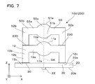
- the joined body 100 includes an optical element 50 that is a third member in addition to the optical element 10 that is the second member and the substrate 20 that is the first member.
- the optical element 50 is overlapped and bonded on the optical element 10. Similar to the optical element 10, the optical element 50 is a transparent and light-transmitting member, and is formed of a polymer material. In the illustrated example, the shape of the optical element 50 is the same as the shape of the optical element 10, but can be changed as appropriate.
- the optical element 50 includes a lens element 50a and a support portion 50b that supports the lens element 50a from the periphery.
- the lens element 50a is, for example, a biconvex aspheric lens, and has a third optical surface 51a and a fourth optical surface 51b.
- the support portion 50b includes a flat plate portion 52a and a square columnar leg portion 52b extending from the flat plate portion 52a in parallel with the optical axis OA.
- the optical element 10 and the optical element 50 are bonded through a bonding layer 230 whose surface is activated. Thereby, the joined body 100 in which the two optical elements 10 and 50 are stacked on the substrate 20 can be obtained. That is, the joined body 100 includes a structure in which two optical elements 10 and 50 are stacked.
- a bonding layer 230 using an inorganic material is formed on the bonding side portion of at least one of the optical elements 10 and 50 (second member) 10, and the surface of the bonding layer 230 or the like is formed in the atmosphere.
- An activation process is performed, and the optical element (second member) 10 and the optical element (third member) 50 are bonded via the bonding layer 30 while the surface of the bonding layer 230 and the like is activated.
- a plurality of optical elements 10 and 50 may be arranged on one substrate 20 as in the second embodiment (see FIG. 8).
- the lens element 10a has a light guide 11g on the substrate 20 side instead of the second optical surface 11b in the first embodiment.
- the light guide portion 11g is columnar and has a flat surface 11c at the lower end.
- the light guide portion 11g may be cylindrical or prismatic, and may or may not have a taper.
- a light shielding portion 11r for preventing the entry of external light is formed.
- the light shielding part 11r is formed, for example, by attaching a black light shielding film, forming a black light shielding film, or applying a texture.
- the light guide 11g corresponds to each lens element 10a. When the light emitting element 22 emits light in the light source unit 200 including the joined body 100, the light passes through the substrate 20, the light guide 11g, and the lens element 10a. Then, the light is emitted from the first optical surface 11a to form an image.
- the flat surface 11c of the optical element 10 and the first surface 20a of the substrate 20 are bonded via a bonding layer 30 whose surface is activated, and the interface between the lens element 10a of the optical element 10 and the substrate 20 is integrally formed. It has become.
- the bonding layer 30 uses a light-transmitting material.
- a plurality of optical elements 10 may be arranged on one substrate 20 as in the second embodiment (see FIG. 9B). Further, as shown in FIG. 9C, the optical element 10 may be provided with a leg portion 12b and bonded to the end surface 12c of the leg portion 12b instead of the flat surface 11c.
- the bonding layer 30 can be made of a metal or a light transmissive material.
- the optical element 10 as the second member is directly molded on the substrate 20 as the first member.
- the bonding layer 30 is formed only on the substrate 20.
- the polymer material forming the optical element 10 is a thermoplastic resin
- the surface of the bonding layer 30 is subjected to an activation process, and then the substrate 20 is injection-molded to mold the optical element 10.
- the polymer material forming the optical element 10 is an energy curable resin or a two-component curable resin
- the surface of the bonding layer 30 is subjected to an activation process, and then the substrate 20 is molded and optically processed.
- the element 10 is molded.
- a polymer material may be applied on the bonding layer 30 that has been activated.
- the bonding layer 30 is formed on the first surface 20 a of the substrate 20.
- an activation process is performed on the surface of the bonding layer 30 on the substrate 20.
- a molding die 90 for molding the optical element 10 is positioned with respect to the substrate 20, and the optical element 10 is in contact with the bonding layer 30 whose surface is activated with respect to the substrate 20. Is molded.
- the optical element 10 is released from the mold 90 to obtain a bonded body 100 in which the optical element 10 and the substrate 20 are bonded via the bonding layer 30 as shown in FIG. 10D.
- the joined body etc. which concern on this embodiment were demonstrated, the joined body etc. which concern on this invention are not restricted to said thing.
- the shape and size of the optical elements 10 and 50 can be changed as appropriate according to the application and function.
- the thicknesses of the first, second, and third members can be changed as appropriate, and may be thick or thin.
- the functions of the first and third members and the second member are not limited to the optical elements 10 and 50 and the substrate 20, but can be changed as appropriate depending on the application. Moreover, according to the use of each member, it is good also as a combination of an optical element and an optical element, or a combination of an optical element and a lens-barrel, for example.
- the optical element 10 is not limited to an array-shaped optical element, and may be one as in the first embodiment.
- a plurality of optical elements 10 having lens elements 10a may be arranged, or a plurality of stacked optical elements 10 and 50 as in the third embodiment may be arranged.
- the joined body 100 of the second embodiment may be cut into individual pieces.
- the optical elements 10 and 50 that are the second and third members are formed of a polymer material at the joining side portion, and the thickness of the polymer material has sufficient flexibility at the time of joining. If it is a thing, the structure (for example, hybrid lens etc.) which combined other materials, such as glass and a metal, may be sufficient.
Landscapes
- Engineering & Computer Science (AREA)
- Mechanical Engineering (AREA)
- Lining Or Joining Of Plastics Or The Like (AREA)
- Wire Bonding (AREA)
- Mounting And Adjusting Of Optical Elements (AREA)
Abstract
複数の部材の接合状態が良好な接合体の製造方法を提供することを目的とする。第1部材である基板20及び高分子材料で形成される第2部材である光学素子10のうち少なくとも基板20の接合側部G2に、無機物を用いた接合層30を形成し、接合層30の表面に活性化処理を施し、接合層30の表面が活性化している状態で大気中において光学素子10と基板20とを接合層30を介して接合する。
Description
本発明は、複数の部材で構成される接合体の製造方法に関する。
接合体の製造方法として、接合する一対の被接合物に設けられた接合部を真空中でエネルギー波により洗浄(表面活性化処理)した後、大気中で常温接合(具体的には、室温~180℃以下での接合)する方法が公知となっている(例えば、特許文献1参照)。特許文献1において、被接合物として銅等の金属や半導体が挙げられ、接合部として表面活性化可能な金属(具体的には、金、アルミ、銅等)や金属以外の材料が挙げられている。特許文献1では、接合界面に金や銅等の比較的柔らかい硬度の金属を介在させるように配置することで、接合界面に施した金属の柔らかさが緩衝材となり、接合界面を平滑化しながら接合している。
また、接合体の別の製造方法として、二酸化ケイ素を含む透明な材料から構成された第1基板と他の基板とを常温接合(具体的には、20℃±15℃での接合)する方法が公知となっている(例えば、特許文献2参照)。特許文献2において、第1基板の一部に設けられた接合層と他の基板の一部に設けられた接合層とを密着させることで、これらの接合層を接合する。接合面への有機物等の吸着による汚染の心配がある場合には、接合層形成後に、加熱、UV光、プラズマ等でクリーニングすることが望ましいとされている。特許文献2の接合層は、常温における酸化物の生成自由エネルギーが正の金属を含む金属材料(具体的には、金、白金、及びこれらの金属を含む合金等)で構成される。また、特許文献2の接合は、大気中でも、減圧環境下又は大気圧以上の雰囲気下でも可能となっている。
しかしながら、特許文献1及び2の接合体の製造方法では、接合する部材が金属や、二酸化ケイ素を含む材料で形成されているため、接合に際して接合面を平滑化できる量が数10nm程度であり、その範囲を超えて接合面に凹凸が存在すると、これらの部材をほとんど接合することができない。
本発明は、複数の部材の接合状態が良好な接合体の製造方法を提供することを目的とする。
上記課題を解決するため、本発明に係る接合体の製造方法は、第1部材及び高分子材料で形成される第2部材のうち少なくとも第1部材の接合側部に、無機物を用いた接合層を形成し、接合層の表面に活性化処理を施し、接合層の表面が活性化している状態で大気中において第1部材と第2部材とを接合層を介して接合する。
上記接合体の製造方法によれば、第2部材が柔軟性を有する高分子材料で形成されているため、各部材の表面形状が数10μm程度のうねりを有していても、接合層で平滑化し、第1及び第2部材を強固に接合することができる。また、第2部材が柔軟性を有するため、第1及び第2部材の厚さに関係なく、接合を達成できる。また、大気中で接合するため、真空引き等の手間を省くことができる。また、接合層が無機物で形成されていることにより、接着剤で接合する場合と比較して収縮等が発生せず、硬化や環境変動で第1及び第2部材間に位置ずれが生じることを防ぐことができる。なお、第1部材に対して第2部材を直接成形する場合には、第1部材上のみに接合層を形成すればよい。一方、第2部材を別途成形した後に第1部材と接合する場合には、第2部材上にも接合層を形成することが望ましい。
〔第1実施形態〕
以下、図面を参照しつつ、本発明の第1実施形態に係る接合体の製造方法によって製造された接合体について説明する。図1A及び1Bに示すように、接合体100は、光学用途に用いられるものであり、第2部材である光学素子10と第1部材である基板20とを有する。光学素子10と基板20とは、基板20が延びるXY面に垂直なZ軸方向に積み重ねられて接合されている。接合体100は、例えば基板20に発光素子22を設けることにより、光源ユニット200として利用することができる。
以下、図面を参照しつつ、本発明の第1実施形態に係る接合体の製造方法によって製造された接合体について説明する。図1A及び1Bに示すように、接合体100は、光学用途に用いられるものであり、第2部材である光学素子10と第1部材である基板20とを有する。光学素子10と基板20とは、基板20が延びるXY面に垂直なZ軸方向に積み重ねられて接合されている。接合体100は、例えば基板20に発光素子22を設けることにより、光源ユニット200として利用することができる。
光学素子10は、利用しようとする波長範囲の光を透過し得る光透過性を有する部材であり、例えば可視光領域の波長の光を透過する場合は透明の部材である。光学素子10は、高分子材料で形成されている。高分子材料としては、例えば熱可塑性樹脂、エネルギー硬化性樹脂、2液硬化性樹脂等が用いられる。熱可塑性樹脂としては、例えばCOP(シクロオレフィンポリマー)、PMMA(アクリル)、PC(ポリカーボネト)等が用いられる。エネルギー硬化性樹脂としては、例えば紫外線硬化性樹脂、熱硬化性樹脂等が用いられる。2液硬化性樹脂としては、例えばエポキシ、シリコーン等が用いられる。光学素子10は、光軸OA方向から見て四角形の輪郭を有する。光学素子10は、レンズ要素10aと、レンズ要素10aを周囲から支持する支持部10bとを有する。レンズ要素10aは、例えば両凸の非球面レンズであり、第1光学面11aと第2光学面11bとを有する。支持部10bは、平板状の平板部分12aと、平板部分12aから光軸OAに平行に延びる一対の脚部分12bとを有する。脚部分12bは、光学素子10と基板20とを接合したい部分に対応して形成されている。図示の例では、脚部分12bは、互いに平行な一対の細長い水平断面を有する四角柱状となっている。なお、脚部分12bの配置及び形状は、支持部10bの平板部分12aを基板20に対して平行かつ安定して保てれば、適宜変更することができる。詳細は後述するが、光学素子10と基板20とは、その表面が活性化した状態で接合されており、光学素子10の脚部分12bと基板20とは接合層30を介して強固に接合されている。光学素子10は、例えば集光レンズとして用いられる。
基板20は、透明で光透過性を有する板状部材であり、無機物であるガラスで形成されたガラス基板である。基板20の表側の第1面20aには、光学素子10が接合されている。また、既に説明したように、図示の例では、基板20の裏側の第2面20bには、発光素子22が設けられている。発光素子22の中心は、光学素子10の光軸OA上に配置される。発光素子22としては、例えば有機ELやLED素子等が用いられる。
光学素子10と基板20との間には、接合層30が設けられている。つまり、成形した光学素子(第2部材)10を、接合層30を介して基板(第1部材)20に接合している。接合層30には、金、銅、銀合金等が用いられる。金の場合、大気中においても活性化の安定性が高く、安定して強固な結合が得られやすい。銅及び銀合金の場合、金よりコストを抑えることができる。また、接合層30には、酸化物、窒化物、フッ化物(例えばSiO、SiO2、TiO、AlN、LaF2、MgF2等)等の可視光を透過させるような光透過性を有する材料を用いてもよい。接合層30の光軸OAに平行な方向の厚さは、好ましくは1nm以上、さらに好ましくは10nm以上である。
接合層30は、光学素子10の脚部分12bに対応する位置に局所的に設けられてもよいし、基板20の第1面20aの全面に設けられてもよい。ここで、光学素子10の接合側部G1と基板20の接合側部G2とに接合層30を形成してこれらを接合する場合には、光学素子10側の接合層30と基板20側の接合層30とは、金属結合等の強固な化学結合によって互いに接合する。このように、接合体100において、光学素子10と基板20とは、接合層30を介して強固な接合状態となるため、耐環境性がよい。接合層30の厚さが数nmの場合、接合層30は膜状とならず島状となるが、膜状の場合よりも接合力が弱くなるものの光学素子10と基板20とを接合できる。各部材10,20と接合層30との境界では、各部材10,20の接合側部G1,G2に金属等が入り込んで混合層が形成されていたり、各部材10,20と接合層30とが化学結合していたりしている。各部材10,20と接合層30との結合力が弱い場合には、部材10,20と接合層30との間に接着層を設けてもよい。また、接合界面にシラノール含有接着剤等、具体的にはシランカップリング剤等を介在させてもよい。また、第2部材である光学素子10側に接合層30を設けなくてもよい。
以下、接合体100の製造方法について説明する。まず、第2部材である光学素子10を成形する。成形方法として、射出成形、型成形等が用いられる。図2Aに示すように、光学素子10の脚部分12bの端面12c(つまり、光学素子10の接合側部G1)に接合層30を形成する。接合層30は、蒸着やスパッタリング等によって形成される。
次に、第1部材である基板20を準備する。図2Bに示すように、基板20の第1面20a(つまり、基板20の接合側部G2)に接合層30を形成する。接合層30は、光学素子10の場合と同様に、蒸着やスパッタリング等によって形成される。なお、光学素子10側の接合層30と、基板20側の接合層30とは、異なる材料で形成されてもよいし、同一の材料で形成されてもよい。また、第1部材である基板20と接合層30とが同一材料の場合は追加で接合層30を設けなくてもよい。
次に、光学素子10上の接合層30及び基板20上の接合層30の双方に対して表面を活性化させる活性化処理を施す。活性化処理として、具体的には、コロナ処理、プラズマ処理、オゾン処理、及び紫外線(UV)処理等を行う。図2C及び2Dに示すように、活性化処理は、光学素子10の脚部分12bの端面12c及び基板20の第1面20aに対して一部又は全体に施される。これにより、光学素子10側の接合層30及び基板20側の接合層30の表面SS1,SS2がそれぞれ活性化され、両者が強固に接合し得る表面状態を得ることができる。活性化処理は、好ましくは、大気中において常温で行うことができる。ここで、常温とは、20℃±15℃を意味する。
なお、接合体100を光源ユニット200の用途で用いる場合には、基板20の第2面20b側に発光素子22を一体的に作り込むだけでなく後工程で取り付けることが考えられる。この場合、上記処理を行う前に発光素子22を基板20に取り付けておくことが好ましい。
次に、光学素子10と基板20とを位置決めする。具体的には、図2Eに示すように、光学素子10側の接合層30と基板20側の接合層30とを対向させ、接合層30の表面を活性化させた状態を維持しつつ、光学素子10と基板20とを隙間をあけた状態で接合位置に配置する。位置決めの際の光学素子10と基板20との間隔は、100nm以上であることが好ましい。また、位置決めにおいて、光学素子10及び基板20のいずれか一方を移動させてもよいし、両者を相対的に移動させてもよい。光学素子10及び基板20には、例えば位置決めのマークが設けられており、マーク位置を合わせることで位置決めを行う。また、光学素子10と基板20とに位置決め基準となる突き当て部を設ければ、当該突き当て部を突き当てることで位置決めすることもできる。
位置決め後、図2Fに示すように、表面を活性化させた状態の接合層30を間に挟むように、光学素子10と基板20とを当接させ接合させる。この接合は、好ましくは、大気中において常温で行う。この際、光学素子10側の接合層30と基板20側の接合層30とが活性化状態において接合界面で互いに強固に結合する。なお、当接の際には、加圧して互いの接合層30を密着させることが好ましい。また、常温より高い温度で接合することも可能である。例えば、常温より高い温度で接合する場合、活性化が向上するため、接合力が増強される。
なお、接合層30が光学素子10の複数の脚部分12bに対応する位置に設けられている場合、光学素子10は、スペースSPをあけて複数個所で基板20に接合された状態となる。これらの脚部分12bは、基板20に対して一括して接合されることになる。
上述した位置決め以後において、光学素子10と基板20とを当接させることで接合を行っが、接合層30の表面を、所定以上の圧力の密着で接合可能となるような活性化状態にして、当接しただけでは接合しないようにしてもよい。この場合、接合層30の表面を、所定以上の圧力の密着で接合可能となるような活性化状態に維持しつつ、光学素子10と基板20とが接触した状態で接合位置に配置させる。その後、光学素子10と基板20とを所定以上の圧力で加圧して接合する。なお、光学素子10と基板20とは、大まかな位置決め後、微小な位置決めの際に接触することが好ましい。
図3A~3Fは、図2A~2Fに示す製造方法の変形例を説明する図である。接合層30として、LaF2、AlN、ITO(スズドープ酸化インジウム)等を用いる場合、これらのいずれかを第1部材としてのガラス板等からなる基板20上に成膜し、活性化処理を行った上で、接合層30を設けずに表面112cを活性化処理した高分子材料からなる第2部材としての平板112bを準備するとともに、基板20及び平板112bを活性化処理面同士が向き合うように当接し、押圧することで、高分子材料のうねりに関わらず、強固な接合力で接合した接合体100を得ることができる。これは、接合層30を構成する材料種と平板112bを形成する高分子の末端基との間で強固な結合が形成されるとともに、平板(第2部材)112bが高分子材料からなるため、各部材20,112bのうねりを吸収して強く接合されるためであると推測される。なお、平板112bは、図1Aに示す光学素子10の一部(例えば脚部分12b)であってもよい。
[実験例1]
以下、具体的な実験例1について説明する。まず、第1部材に相当する帯状のガラス板と第2部材に相当する帯状の樹脂平板とを準備する。帯状のガラス板(BK7、幅4mm×長さ15mm、厚み1mm、うねり:PV 1nm)の片面に、スパッタリング装置を用いて接合層となるべき金を20nmの厚さに成膜した。このとき、ガラス板と金との接合を良くするための密着層として、金の成膜に先立って、スパッタリング装置を用いてクロムをガラス板上に10nmの厚さ成膜した。また、帯状のポリカーボネート製平板(タキロン社製PC 1600、幅4mm×長さ10mm、厚み2mm、うねり:PV 12μm)に、スパッタリング装置を用いて接合層となるべき金を20nm成膜した。そして、金が成膜された樹脂平板及び金が成膜されたガラス板を、いずれも金が成膜された面を上にしてプラズマ発生装置に入れて、真空度が0.3Mpa、プラズマガスN2の流量が100ml/min、プラズマ出力が200Wの条件で、金に対する活性化処理を行った。活性化処理後、プラズマ発生装置を大気解放し、30分以内に接合位置を合わせ、樹脂平板及びガラス板の活性化処理された面同士を、重ねあわせ方向から見て十字になるように当接させた。そして、当接と同時に100Nの押圧力で10sec加圧することで接合を完了させた。こうして得られた接合体をガラス板が上になるように配置し、さらに、ガラス板を跨ぐようにゲタ状の加圧治具を配置し、この加圧治具を介して樹脂平板の両端をプッシュゲージ(SIMPO社製FGP-50)で加圧することで、両者が剥離する方向に力を加えた。その結果、20MPaまで引張り力を印加しても両者を剥離することはできず、両者が強固に接合していることを確認できた。なお、20MPaを超える引張り力を印加すると接合体は破断した。
以下、具体的な実験例1について説明する。まず、第1部材に相当する帯状のガラス板と第2部材に相当する帯状の樹脂平板とを準備する。帯状のガラス板(BK7、幅4mm×長さ15mm、厚み1mm、うねり:PV 1nm)の片面に、スパッタリング装置を用いて接合層となるべき金を20nmの厚さに成膜した。このとき、ガラス板と金との接合を良くするための密着層として、金の成膜に先立って、スパッタリング装置を用いてクロムをガラス板上に10nmの厚さ成膜した。また、帯状のポリカーボネート製平板(タキロン社製PC 1600、幅4mm×長さ10mm、厚み2mm、うねり:PV 12μm)に、スパッタリング装置を用いて接合層となるべき金を20nm成膜した。そして、金が成膜された樹脂平板及び金が成膜されたガラス板を、いずれも金が成膜された面を上にしてプラズマ発生装置に入れて、真空度が0.3Mpa、プラズマガスN2の流量が100ml/min、プラズマ出力が200Wの条件で、金に対する活性化処理を行った。活性化処理後、プラズマ発生装置を大気解放し、30分以内に接合位置を合わせ、樹脂平板及びガラス板の活性化処理された面同士を、重ねあわせ方向から見て十字になるように当接させた。そして、当接と同時に100Nの押圧力で10sec加圧することで接合を完了させた。こうして得られた接合体をガラス板が上になるように配置し、さらに、ガラス板を跨ぐようにゲタ状の加圧治具を配置し、この加圧治具を介して樹脂平板の両端をプッシュゲージ(SIMPO社製FGP-50)で加圧することで、両者が剥離する方向に力を加えた。その結果、20MPaまで引張り力を印加しても両者を剥離することはできず、両者が強固に接合していることを確認できた。なお、20MPaを超える引張り力を印加すると接合体は破断した。
比較のため、上記樹脂平板及び上記ガラス板のいずれにも金を成膜せずに両者を大気中で当接させて100Nの押圧力で10sec加圧したが、両者を接合することはできなかった。また、上記樹脂平板及び上記ガラス板のいずれにも金を成膜せず、上述したのと同様の条件で活性化処理を行った後、両者の活性化処理面同士を向き合わせて大気中で当接させて100Nの押圧力で10sec加圧したが、やはり両者を接合することはできなかった。
[実験例2]
実験例2について説明する。まず、第1部材に相当する帯状のガラス板(BK7、幅4mm×長さ15mm、厚み1mm、うねり:PV 1nm)と、第2部材に相当する帯状のポリカーボネート製平板(タキロン社製PC 1600、幅4mm×長さ10mm、厚み2mm、うねり:PV 12μm)とを準備し、帯状のガラス板の表面にスパッタリング装置を用いて接合層となるべきLaF2を50nmの厚さに成膜する。そして、上記ガラス板と上記樹脂平板とをプラズマ発生装置にセットした。この際、ガラス板のLaF2が成膜された面を上にした。プラズマ発生装置により、ガラス板及び樹脂平板に対して、真空度が0.3Mpa、プラズマガスN2の流量が100ml/min、プラズマ出力が200Wの条件で活性化処理を行った。活性化処理後、プラズマ発生装置を大気解放し、30分以内に接合位置を合わせ、樹脂平板及びガラス板の活性化処理された面同士を、重ねあわせ方向から見て十字になるように当接させた。そして、当接と同時に100Nの押圧力で10sec加圧することで接合を完了させた。こうして得られた接合体をガラス板が上になるように配置し、さらに、ガラス板を跨ぐようにゲタ状の加圧治具を配置し、この加圧治具を介して樹脂平板をプッシュゲージ(SIMPO社製FGP-50)で加圧することで、両者が剥離する方向に力を加えた。その結果、20MPaまで引張り力を印加しても両者を剥がすことはできず、20MPaを超える引張り力が印加されたところで接合体が破断した。
実験例2について説明する。まず、第1部材に相当する帯状のガラス板(BK7、幅4mm×長さ15mm、厚み1mm、うねり:PV 1nm)と、第2部材に相当する帯状のポリカーボネート製平板(タキロン社製PC 1600、幅4mm×長さ10mm、厚み2mm、うねり:PV 12μm)とを準備し、帯状のガラス板の表面にスパッタリング装置を用いて接合層となるべきLaF2を50nmの厚さに成膜する。そして、上記ガラス板と上記樹脂平板とをプラズマ発生装置にセットした。この際、ガラス板のLaF2が成膜された面を上にした。プラズマ発生装置により、ガラス板及び樹脂平板に対して、真空度が0.3Mpa、プラズマガスN2の流量が100ml/min、プラズマ出力が200Wの条件で活性化処理を行った。活性化処理後、プラズマ発生装置を大気解放し、30分以内に接合位置を合わせ、樹脂平板及びガラス板の活性化処理された面同士を、重ねあわせ方向から見て十字になるように当接させた。そして、当接と同時に100Nの押圧力で10sec加圧することで接合を完了させた。こうして得られた接合体をガラス板が上になるように配置し、さらに、ガラス板を跨ぐようにゲタ状の加圧治具を配置し、この加圧治具を介して樹脂平板をプッシュゲージ(SIMPO社製FGP-50)で加圧することで、両者が剥離する方向に力を加えた。その結果、20MPaまで引張り力を印加しても両者を剥がすことはできず、20MPaを超える引張り力が印加されたところで接合体が破断した。
以上説明した第1実施形態の接合体の製造方法によれば、第2部材である光学素子10が柔軟性を有する高分子材料で形成されているため、各部材10,20が数10μm程度のうねりを有していても、当接の際の加圧により接合層30で平滑化し、第1部材である基板20及び第2部材である光学素子10を強固に接合することができる。また、光学素子10が柔軟性を有するため、光学素子10及び基板20の厚さに関係なく、接合を達成できる。また、大気中で接合するため、真空引き等の手間を省くことができる。また、接合層30が無機物で形成されていることにより、接着剤で接合する場合と比較して収縮等が発生せず、硬化や環境変動で光学素子10及び基板20間に位置ずれが生じることを防ぐことができる。また、特に異なる材料を使用環境温度、例えば、常温で接合できるため、使用時の線膨張差による応力や剥がれを抑制することができる。
また、光学素子10及び基板20が透明で光透過性を有する部材であっても、表面を活性化させた接合層30を介して接合するため、接合状態が良好となる。つまり、光学素子10及び基板20の色に関係なく接合でき、両者は透明な部材に限らず、例えば黒色の部材を用いてもよい。
また、表面を活性化させた接合層30を介して行う接合は、光透過性を有し、歪みを嫌う、耐環境性を有する部材、特に位置ずれに関して重要度が高いものの接合に適合しており、光学素子10と基板20とを組み合わせた接合体100でも良好な接合状態を達成でき維持できる。
〔第2実施形態〕
以下、第2実施形態に係る接合体の製造方法について説明する。なお、第2実施形態に係る接合体の製造方法は、第1実施形態の接合体の製造方法を一部変更したものであり、特に説明しない事項は、第1実施形態と同様である。
以下、第2実施形態に係る接合体の製造方法について説明する。なお、第2実施形態に係る接合体の製造方法は、第1実施形態の接合体の製造方法を一部変更したものであり、特に説明しない事項は、第1実施形態と同様である。
図4A、4B、及び図5Aに示すように、本実施形態では、1つの第1部材である基板20に複数の第2部材である光学素子10が接合層30を介して接合されている。また、基板20と光学素子10との間には、遮光体40が設けられている。接合体100を含む光源ユニット200は、例えばプリントヘッド等に用いられる。
1つの光学素子10は、光軸OA方向から見て四角形の輪郭を有する。光学素子10は、複数のレンズ要素10aと、これら複数のレンズ要素10aを周囲から支持する支持部10bとを有する。レンズ要素10aは、アレイ状に設けられている。支持部10bは、平板状の外形を有する平板部分12aの対向する2つの辺から平板部分12aに垂直な方向に延びる脚部分12bを有する。
基板20の第2面20bには、複数の発光素子22が光学素子10のレンズ要素10aに対応する位置にアレイ状に設けられている。なお、発光素子22は、基板20の第2面20b側に限らず、表の第1面20a側に設けることができる。
遮光体40は、平板状の部材であり、発光素子22の不要光を遮光する。遮光体40としては、例えば黒色等の光吸収性の粒子を含むガラス製又は樹脂製の基板、黒色に塗装された金属製の基板等を用いる。遮光体40には、光学素子10のレンズ要素10aに対応する位置に開口40aが形成されている。図5Aの例では、遮光体40は、基板20側に接合されている。遮光体40は、接着剤で接着されてもよいが、材料の組み合わせによって、光学素子10と基板20との接合と同様に、表面を活性化させた接合層を利用して接合させてもよい。例えば、遮光体40の材料が樹脂製である場合、表面を活性化させた接合層130を介して接合することができる。
図4Bの例では、光学素子10の個片数と同じ数の遮光体40を並べているが、光学的に許容できていれば、光学素子10よりも少ない数を並べてもよく、又は全体として1つの板状部材を用いてもよい。
接合体100の製造において、基板20の第1面20a上に複数の光学素子10を全て並べた状態で、一度に接合させてもよいし、1個又は数個単位で光学素子10を並べて複数回に分けて接合させてもよい。
以上説明した接合体100では、表面を活性化させた状態での接合は比較的短時間で行うことができるため、複数の光学素子10を一度に、又は複数回に分けて接合させても比較的短時間で接合でき、生産性が良い。
図6に示すように、接合体100を含む光源ユニット200は、例えば画像形成装置である電子写真式プリンターに内蔵される作像ユニット80内に組み込まれる。作像ユニット80は、現像用のトナーを用紙に転写するためのものである。作像ユニット80には、感光体81と、帯電ローラー82と、プリントヘッド83と、現像装置84と、転写装置85と、クリーニング装置86と、除電装置87とが設けられている。光源ユニット200は、これらのうちプリントヘッド83内に組み込まれて露光を行う。作像ユニット80において、感光体81に対し上記他の部材82~87が作用することで、用紙PPに対し画像が形成される。
なお、上記実施形態において、図5Bに示すように、遮光体40は、基板20側に接合する場合に限らず、光学素子10側に接合してもよい。この場合、遮光体40の材料が、樹脂、ガラス、及び金属のいずれであっても、接合層130を介して光学素子10に接合することができる。また、図5Cに示すように、光学素子10の脚部分12bに遮光体40を保持させるような構成としてもよい。
〔第3実施形態〕
以下、第3実施形態に係る接合体の製造方法について説明する。なお、第3実施形態に係る接合体の製造方法は、第1実施形態の接合体の製造方法を一部変更したものであり、特に説明しない事項は、第1実施形態と同様である。
以下、第3実施形態に係る接合体の製造方法について説明する。なお、第3実施形態に係る接合体の製造方法は、第1実施形態の接合体の製造方法を一部変更したものであり、特に説明しない事項は、第1実施形態と同様である。
図7に示すように、本実施形態において、接合体100は、第2部材である光学素子10及び第1部材である基板20の他に、第3部材である光学素子50を有する。光学素子50は、光学素子10上に重ねて接合されている。光学素子50は、光学素子10と同様に、透明で光透過性を有する部材であり、高分子材料で形成されている。図示の例では、光学素子50の形状は、光学素子10の形状と同様であるが、適宜変更することができる。光学素子50は、レンズ要素50aと、レンズ要素50aを周囲から支持する支持部50bとを有する。レンズ要素50aは、例えば両凸の非球面レンズであり、第3光学面51aと第4光学面51bとを有する。支持部50bは、平板状の平板部分52aと、平板部分52aから光軸OAに平行に延びる四角柱状の脚部分52bとを有する。光学素子10と光学素子50とは表面を活性化させた接合層230を介して接合されている。これにより、基板20上に、2つの光学素子10,50を積み重ねた接合体100を得ることができる。つまり、接合体100は2つの光学素子10,50を積層したものを含む構成となっている。製造に際しては、両光学素子10,50のうち少なくとも一方の光学素子(第2部材)10の接合側部に、無機物を用いた接合層230を形成し、大気中において接合層230等の表面に活性化処理を施し、接合層230等の表面が活性化している状態で光学素子(第2部材)10と光学素子(第3部材)50とを接合層30を介して接合する。
なお、本実施形態においても、第2実施形態のように、1つの基板20に複数の光学素子10,50を並べてもよい(図8参照)。
〔第4実施形態〕
以下、第4実施形態に係る接合体の製造方法について説明する。なお、第4実施形態に係る接合体の接合方法は、第1実施形態の接合体の接合方法を一部変更したものであり、特に説明しない事項は、第1実施形態と同様である。
以下、第4実施形態に係る接合体の製造方法について説明する。なお、第4実施形態に係る接合体の接合方法は、第1実施形態の接合体の接合方法を一部変更したものであり、特に説明しない事項は、第1実施形態と同様である。
図9Aに示すように、光学素子10において、レンズ要素10aは、基板20側に、第1実施形態における第2光学面11bに代えて、導光部11gを有する。導光部11gは、柱状であり、下端部に平坦面11cを有している。導光部11gは、円柱状でも角柱状でもよく、テーパーを有していても有していなくてもよい。導光部11gの側面には、外光の侵入を防ぐための遮光部11rが形成されている。遮光部11rは、例えば黒色の遮光フィルムを貼り付けたり、黒色の遮光膜を成膜したり、シボ加工を施すことで形成する。導光部11gは、個々のレンズ要素10aに対応しており、接合体100を含む光源ユニット200において発光素子22が発光すると、その光は基板20、導光部11g、及びレンズ要素10aを通過して第1光学面11aから射出され、結像する。
光学素子10の平坦面11cと基板20の第1面20aとが表面を活性化させた接合層30を介して接合しており、光学素子10のレンズ要素10a及び基板20の界面は一体的になっている。図9Aの例では、接合層30は、光透過性を有する材料を用いる。
なお、本実施形態においても、第2実施形態のように、1つの基板20に複数の光学素子10を並べてもよい(図9B参照)。また、図9Cに示すように、光学素子10に脚部分12bを設け、平坦面11cでなく、脚部分12bの端面12cで接合させてもよい。なお、図9Cの例では、第1実施形態の場合と同様に、接合層30は、金属や光透過性を有する材料を用いることができる。
〔第5実施形態〕
以下、第5実施形態に係る接合体の製造方法について説明する。なお、第5実施形態に係る接合体の製造方法は、第1実施形態の接合体の製造方法を一部変更したものであり、特に説明しない事項は、第1実施形態と同様である。
以下、第5実施形態に係る接合体の製造方法について説明する。なお、第5実施形態に係る接合体の製造方法は、第1実施形態の接合体の製造方法を一部変更したものであり、特に説明しない事項は、第1実施形態と同様である。
本実施形態において、第1部材である基板20に対して第2部材である光学素子10を直接成形する。この場合、基板20上のみに接合層30を形成する。光学素子10を形成する高分子材料が熱可塑性樹脂である場合、接合層30の表面に活性化処理を施した後に基板20に対して射出成形を行って光学素子10を成形する。また、光学素子10を形成する高分子材料がエネルギー硬化性樹脂や2液硬化性樹脂である場合、接合層30の表面に活性化処理を施した後に基板20に対して型成形を行って光学素子10を成形する。なお、第2部材が型による成形を必要としない場合、活性化処理を施した接合層30上に高分子材料を塗布してもよい。
以下、本実施形態の接合体100の製造方法について説明する。まず、図10Aに示すように、基板20の第1面20aに接合層30を形成する。次に、図10Bに示すように、基板20上の接合層30の表面に対して活性化処理を施す。その後、図10Cに示すように、光学素子10を成形するための成形型90を基板20に対して位置決めし、基板20に対し表面が活性化した状態の接合層30に接するように光学素子10を成形する。成形後、成形型90から光学素子10を離型することにより、図10Dに示すような光学素子10と基板20とが接合層30を介して接合した接合体100を得る。
以上、本実施形態に係る接合体等について説明したが、本発明に係る接合体等は上記のものには限られない。例えば、上記実施形態において、光学素子10,50の形状及び大きさは、用途や機能に応じて適宜変更することができる。
また、上記実施形態において、第1、第2、及び第3部材の厚さは、適宜変更することができ、厚くても薄くてもよい。
また、上記実施形態において、第1及び第3部材及び第2部材は、それぞれ光学素子10,50及び基板20に限らず、用途に応じて適宜機能等を変更することができる。また、各部材の用途に応じて、例えば光学素子と光学素子との組み合わせや、光学素子と鏡筒との組み合わせとしてもよい。
また、第2実施形態において、1つの基板20に複数の光学素子10を配置する例を挙げたが、光学素子10は、アレイ状の光学素子に限らず、第1実施形態のような1つのレンズ要素10aを有する光学素子10を複数並べてもよいし、第3実施形態のような光学素子10,50を積み重ねたものを複数並べてもよい。また、第2実施形態の接合体100を切断して、接合体を個片化してもよい。
また、上記実施形態において、第2及び第3部材である光学素子10,50は、接合側部が高分子材料で形成されており、高分子材料の厚さが接合時に十分な柔軟性を有するものであれば、ガラスや金属等の他の材料を組み合わせた構造(例えば、ハイブリッドレンズ等)であってもよい。
Claims (14)
- 第1部材及び高分子材料で形成される第2部材のうち少なくとも前記第1部材の接合側部に、無機物を用いた接合層を形成し、
前記接合層の表面に活性化処理を施し、
前記接合層の表面が活性化している状態で大気中において前記第1部材と前記第2部材とを前記接合層を介して接合する、接合体の製造方法。 - 前記接合層は、金、銅、及び銀合金のいずれかで形成される、請求項1に記載の接合体の製造方法。
- 前記活性化処理は、コロナ処理、プラズマ処理、オゾン処理、及び紫外線処理のいずれかである、請求項1及び2のいずれか一項に記載の接合体の製造方法。
- 前記高分子材料は、熱可塑性樹脂、エネルギー硬化性樹脂、及び2液硬化性樹脂のいずれかである、請求項1から3までのいずれか一項に記載の接合体の製造方法。
- 前記第2部材及び前記接合層の少なくとも一方は、光透過性を有する材料で形成される、請求項1から4までのいずれか一項に記載の接合体の製造方法。
- 前記第2部材は、光学素子である、請求項5に記載の接合体の製造方法。
- 前記第1部材は、ガラス板である、請求項6に記載の接合体の製造方法。
- 前記第2部材及び高分子材料で形成された光学素子である第3部材のうち少なくとも前記第2部材の接合側部に、無機物を用いた接合層を形成し、
大気中において前記接合層の表面に活性化処理を施し、
前記第2部材の接合側部に形成した前記接合層の表面が活性化している状態で前記第2部材と前記第3部材とを前記第2部材の接合側部に形成した前記接合層を介して接合する、請求項7に記載の接合体の製造方法。 - 複数の前記光学素子を接合する、請求項6から8までのいずれか一項に記載の接合体の製造方法。
- 前記接合層の表面を活性化させた状態を維持しつつ、前記第1部材と前記第2部材とを隙間をあけた状態で接合位置に配置した後、前記第1部材と前記第2部材とを当接させて接合する、請求項1から9までのいずれか一項に記載の接合体の製造方法。
- 前記接合層の表面を、所定以上の圧力の密着によって接合可能な活性化状態に維持しつつ、前記第1部材と前記第2部材とが接触した状態で接合位置に配置された後、前記第1部材と前記第2部材とを前記所定以上の圧力で加圧して接合する、請求項1から9までのいずれか一項に記載の接合体の製造方法。
- 前記第1部材と前記第2部材とを個別に準備した後、前記第1部材及び前記第2部材の双方に前記接合層を形成し、両部材に設けた前記各接合層を接触させて前記第1部材と前記第2部材とを接合する、請求項1から11までのいずれか一項に記載の接合体の製造方法。
- スペースをあけて複数個所で接合する、請求項1から12までのいずれか一項に記載の接合体の製造方法。
- 前記第1部材上に前記接合層を形成した後、前記第2部材を構成する材料を用いて前記第1部材上の前記接合層の形成面上に前記第2部材を成形する、請求項1から9までのいずれか一項に記載の接合体の製造方法。
Priority Applications (2)
| Application Number | Priority Date | Filing Date | Title |
|---|---|---|---|
| JP2017555981A JP6751273B2 (ja) | 2015-12-14 | 2016-12-02 | 接合体の製造方法 |
| CN201680073098.0A CN108472877B (zh) | 2015-12-14 | 2016-12-02 | 接合体的制造方法 |
Applications Claiming Priority (2)
| Application Number | Priority Date | Filing Date | Title |
|---|---|---|---|
| JP2015243640 | 2015-12-14 | ||
| JP2015-243640 | 2015-12-14 |
Publications (1)
| Publication Number | Publication Date |
|---|---|
| WO2017104453A1 true WO2017104453A1 (ja) | 2017-06-22 |
Family
ID=59056452
Family Applications (1)
| Application Number | Title | Priority Date | Filing Date |
|---|---|---|---|
| PCT/JP2016/085977 Ceased WO2017104453A1 (ja) | 2015-12-14 | 2016-12-02 | 接合体の製造方法 |
Country Status (3)
| Country | Link |
|---|---|
| JP (1) | JP6751273B2 (ja) |
| CN (1) | CN108472877B (ja) |
| WO (1) | WO2017104453A1 (ja) |
Citations (8)
| Publication number | Priority date | Publication date | Assignee | Title |
|---|---|---|---|---|
| JPS60264230A (ja) * | 1984-06-14 | 1985-12-27 | Toyo Ink Mfg Co Ltd | ポリエステル基材の接合方法 |
| JP2003001455A (ja) * | 2001-06-15 | 2003-01-08 | Matsushita Electric Ind Co Ltd | 金属と樹脂との接合方法及び装置、制振鋼板の製造方法 |
| JP2003291256A (ja) * | 2002-03-29 | 2003-10-14 | Nitto Boseki Co Ltd | 銅箔/樹脂積層体の製造方法 |
| WO2008006586A1 (en) * | 2006-07-14 | 2008-01-17 | Borealis Technology Oy | Polymer blend |
| JP2010106081A (ja) * | 2008-10-28 | 2010-05-13 | Seiko Epson Corp | 接合方法、接合体および光学素子 |
| JP2011020905A (ja) * | 2009-07-17 | 2011-02-03 | Tss Kk | 接合部材の製造方法 |
| JP2014163818A (ja) * | 2013-02-26 | 2014-09-08 | Kyushu Univ | マイクロチップを用いた光分析方法および光分析装置、ならびに光分析装置用マイクロチップおよび光分析用処理装置 |
| JP2014177026A (ja) * | 2013-03-14 | 2014-09-25 | Honda Motor Co Ltd | 異種材接合品及びその製造方法 |
Family Cites Families (3)
| Publication number | Priority date | Publication date | Assignee | Title |
|---|---|---|---|---|
| JP3848989B2 (ja) * | 2003-05-15 | 2006-11-22 | 唯知 須賀 | 基板接合方法および基板接合装置 |
| CN101542293B (zh) * | 2006-12-01 | 2012-10-03 | 柯尼卡美能达精密光学株式会社 | 微芯片衬底的接合方法以及微芯片 |
| JP2013210490A (ja) * | 2012-03-30 | 2013-10-10 | Konica Minolta Inc | 光学素子及び補助光源ユニット |
-
2016
- 2016-12-02 WO PCT/JP2016/085977 patent/WO2017104453A1/ja not_active Ceased
- 2016-12-02 CN CN201680073098.0A patent/CN108472877B/zh active Active
- 2016-12-02 JP JP2017555981A patent/JP6751273B2/ja active Active
Patent Citations (8)
| Publication number | Priority date | Publication date | Assignee | Title |
|---|---|---|---|---|
| JPS60264230A (ja) * | 1984-06-14 | 1985-12-27 | Toyo Ink Mfg Co Ltd | ポリエステル基材の接合方法 |
| JP2003001455A (ja) * | 2001-06-15 | 2003-01-08 | Matsushita Electric Ind Co Ltd | 金属と樹脂との接合方法及び装置、制振鋼板の製造方法 |
| JP2003291256A (ja) * | 2002-03-29 | 2003-10-14 | Nitto Boseki Co Ltd | 銅箔/樹脂積層体の製造方法 |
| WO2008006586A1 (en) * | 2006-07-14 | 2008-01-17 | Borealis Technology Oy | Polymer blend |
| JP2010106081A (ja) * | 2008-10-28 | 2010-05-13 | Seiko Epson Corp | 接合方法、接合体および光学素子 |
| JP2011020905A (ja) * | 2009-07-17 | 2011-02-03 | Tss Kk | 接合部材の製造方法 |
| JP2014163818A (ja) * | 2013-02-26 | 2014-09-08 | Kyushu Univ | マイクロチップを用いた光分析方法および光分析装置、ならびに光分析装置用マイクロチップおよび光分析用処理装置 |
| JP2014177026A (ja) * | 2013-03-14 | 2014-09-25 | Honda Motor Co Ltd | 異種材接合品及びその製造方法 |
Also Published As
| Publication number | Publication date |
|---|---|
| CN108472877A (zh) | 2018-08-31 |
| JP6751273B2 (ja) | 2020-09-02 |
| JPWO2017104453A1 (ja) | 2018-09-27 |
| CN108472877B (zh) | 2021-01-05 |
Similar Documents
| Publication | Publication Date | Title |
|---|---|---|
| KR102131962B1 (ko) | 커버 윈도우의 제조장치 및 커버 윈도우의 제조방법 | |
| US10082603B2 (en) | Optical component production method, optical component, and optical panel production method | |
| CN101290445A (zh) | 曲面显示面板及其制造方法 | |
| US20120275024A1 (en) | Polarizer assembly with adhesive layers | |
| WO2017216898A1 (ja) | 内視鏡用光学ユニットの製造方法、内視鏡用光学ユニット、および内視鏡 | |
| WO2017043456A1 (ja) | 光制御パネルの製造方法、光制御パネル、光学結像装置、及び、空中映像形成システム | |
| CN112739516B (zh) | 柔性模具的制造方法、柔性模具用的基材、以及光学部件的制造方法 | |
| WO2017104453A1 (ja) | 接合体の製造方法 | |
| CN108091256B (zh) | 显示器模块及其制造方法 | |
| EP3318390A1 (en) | Bonded body and method for producing bonded body | |
| JP7060845B2 (ja) | フレキシブルモールドの製造方法、フレキシブルモールド用の基材、及び光学部品の製造方法 | |
| WO2017138364A1 (ja) | 液晶表示装置 | |
| WO2021070400A1 (ja) | 光学結像装置及びその製造方法 | |
| JPH0486100A (ja) | 超音波探触子およびその製造方法 | |
| JPWO2017002973A1 (ja) | 接合体及び接合体の製造方法 | |
| CN103376493A (zh) | 导光板及其制作方法 | |
| WO2023007616A1 (ja) | レンズユニットの製造方法、レンズユニット、撮像装置、および、内視鏡 | |
| TW200815907A (en) | Lens module and method for manufacturing same | |
| JP2006258999A (ja) | 光メモリの製造方法 | |
| JP2017209910A (ja) | 複合基材の製造方法 | |
| JP2003123483A (ja) | 光透過性スタンパ及びその製造方法並びに光メモリ素子の製造方法 |
Legal Events
| Date | Code | Title | Description |
|---|---|---|---|
| 121 | Ep: the epo has been informed by wipo that ep was designated in this application |
Ref document number: 16875436 Country of ref document: EP Kind code of ref document: A1 |
|
| ENP | Entry into the national phase |
Ref document number: 2017555981 Country of ref document: JP Kind code of ref document: A |
|
| NENP | Non-entry into the national phase |
Ref country code: DE |
|
| 122 | Ep: pct application non-entry in european phase |
Ref document number: 16875436 Country of ref document: EP Kind code of ref document: A1 |