WO2017090211A1 - Microscope - Google Patents
Microscope Download PDFInfo
- Publication number
- WO2017090211A1 WO2017090211A1 PCT/JP2015/083511 JP2015083511W WO2017090211A1 WO 2017090211 A1 WO2017090211 A1 WO 2017090211A1 JP 2015083511 W JP2015083511 W JP 2015083511W WO 2017090211 A1 WO2017090211 A1 WO 2017090211A1
- Authority
- WO
- WIPO (PCT)
- Prior art keywords
- imaging
- imaging position
- image
- optical system
- dimensional image
- Prior art date
Links
- 238000003384 imaging method Methods 0.000 claims abstract description 271
- 230000003287 optical effect Effects 0.000 claims abstract description 125
- 230000005284 excitation Effects 0.000 claims abstract description 46
- 239000000463 material Substances 0.000 claims abstract description 29
- 238000005286 illumination Methods 0.000 claims abstract description 21
- 201000009310 astigmatism Diseases 0.000 claims abstract description 16
- 230000003213 activating effect Effects 0.000 claims abstract 4
- 239000000126 substance Substances 0.000 claims description 32
- 238000000034 method Methods 0.000 claims description 27
- 239000003086 colorant Substances 0.000 claims description 9
- 230000004913 activation Effects 0.000 abstract description 41
- 239000000975 dye Substances 0.000 description 23
- 238000010586 diagram Methods 0.000 description 21
- 230000005484 gravity Effects 0.000 description 21
- 238000002073 fluorescence micrograph Methods 0.000 description 18
- 239000012190 activator Substances 0.000 description 7
- 239000006059 cover glass Substances 0.000 description 6
- 239000007850 fluorescent dye Substances 0.000 description 5
- 230000012447 hatching Effects 0.000 description 4
- 238000009825 accumulation Methods 0.000 description 3
- 230000000903 blocking effect Effects 0.000 description 3
- 102000034287 fluorescent proteins Human genes 0.000 description 3
- 108091006047 fluorescent proteins Proteins 0.000 description 3
- 230000004807 localization Effects 0.000 description 3
- 238000000386 microscopy Methods 0.000 description 3
- 238000006243 chemical reaction Methods 0.000 description 2
- ANRHNWWPFJCPAZ-UHFFFAOYSA-M thionine Chemical compound [Cl-].C1=CC(N)=CC2=[S+]C3=CC(N)=CC=C3N=C21 ANRHNWWPFJCPAZ-UHFFFAOYSA-M 0.000 description 2
- WSFSSNUMVMOOMR-UHFFFAOYSA-N Formaldehyde Chemical compound O=C WSFSSNUMVMOOMR-UHFFFAOYSA-N 0.000 description 1
- 230000005540 biological transmission Effects 0.000 description 1
- 238000005562 fading Methods 0.000 description 1
- 239000008098 formaldehyde solution Substances 0.000 description 1
- 230000003834 intracellular effect Effects 0.000 description 1
- 239000004973 liquid crystal related substance Substances 0.000 description 1
- 238000012986 modification Methods 0.000 description 1
- 230000004048 modification Effects 0.000 description 1
- 239000013307 optical fiber Substances 0.000 description 1
- 210000001747 pupil Anatomy 0.000 description 1
- 239000007787 solid Substances 0.000 description 1
Images


Classifications
-
- G—PHYSICS
- G02—OPTICS
- G02B—OPTICAL ELEMENTS, SYSTEMS OR APPARATUS
- G02B21/00—Microscopes
- G02B21/16—Microscopes adapted for ultraviolet illumination ; Fluorescence microscopes
-
- G—PHYSICS
- G01—MEASURING; TESTING
- G01N—INVESTIGATING OR ANALYSING MATERIALS BY DETERMINING THEIR CHEMICAL OR PHYSICAL PROPERTIES
- G01N21/00—Investigating or analysing materials by the use of optical means, i.e. using sub-millimetre waves, infrared, visible or ultraviolet light
- G01N21/62—Systems in which the material investigated is excited whereby it emits light or causes a change in wavelength of the incident light
- G01N21/63—Systems in which the material investigated is excited whereby it emits light or causes a change in wavelength of the incident light optically excited
- G01N21/64—Fluorescence; Phosphorescence
- G01N21/645—Specially adapted constructive features of fluorimeters
- G01N21/6456—Spatial resolved fluorescence measurements; Imaging
- G01N21/6458—Fluorescence microscopy
-
- G—PHYSICS
- G01—MEASURING; TESTING
- G01N—INVESTIGATING OR ANALYSING MATERIALS BY DETERMINING THEIR CHEMICAL OR PHYSICAL PROPERTIES
- G01N21/00—Investigating or analysing materials by the use of optical means, i.e. using sub-millimetre waves, infrared, visible or ultraviolet light
- G01N21/62—Systems in which the material investigated is excited whereby it emits light or causes a change in wavelength of the incident light
- G01N21/63—Systems in which the material investigated is excited whereby it emits light or causes a change in wavelength of the incident light optically excited
- G01N21/64—Fluorescence; Phosphorescence
-
- G—PHYSICS
- G02—OPTICS
- G02B—OPTICAL ELEMENTS, SYSTEMS OR APPARATUS
- G02B21/00—Microscopes
- G02B21/0004—Microscopes specially adapted for specific applications
- G02B21/002—Scanning microscopes
- G02B21/0024—Confocal scanning microscopes (CSOMs) or confocal "macroscopes"; Accessories which are not restricted to use with CSOMs, e.g. sample holders
- G02B21/0052—Optical details of the image generation
- G02B21/0076—Optical details of the image generation arrangements using fluorescence or luminescence
-
- G—PHYSICS
- G02—OPTICS
- G02B—OPTICAL ELEMENTS, SYSTEMS OR APPARATUS
- G02B21/00—Microscopes
- G02B21/36—Microscopes arranged for photographic purposes or projection purposes or digital imaging or video purposes including associated control and data processing arrangements
- G02B21/365—Control or image processing arrangements for digital or video microscopes
- G02B21/367—Control or image processing arrangements for digital or video microscopes providing an output produced by processing a plurality of individual source images, e.g. image tiling, montage, composite images, depth sectioning, image comparison
-
- H—ELECTRICITY
- H04—ELECTRIC COMMUNICATION TECHNIQUE
- H04N—PICTORIAL COMMUNICATION, e.g. TELEVISION
- H04N23/00—Cameras or camera modules comprising electronic image sensors; Control thereof
-
- G—PHYSICS
- G01—MEASURING; TESTING
- G01N—INVESTIGATING OR ANALYSING MATERIALS BY DETERMINING THEIR CHEMICAL OR PHYSICAL PROPERTIES
- G01N2201/00—Features of devices classified in G01N21/00
- G01N2201/06—Illumination; Optics
- G01N2201/061—Sources
- G01N2201/06113—Coherent sources; lasers
Definitions
- the present invention relates to a microscope apparatus, an imaging method, and a program.
- Patent Document 1 US Patent Application Publication No. 2008/0182336
- an activation light that activates a part of the fluorescent substance contained in the sample, and an illumination optical system that emits excitation light that excites at least a part of the activated fluorescent substance
- An imaging optical system having an objective lens and an astigmatism optical system for generating astigmatism with respect to at least a part of the fluorescence from the fluorescent material, and an imaging optical system
- a microscope having an imaging unit that captures the captured image, a drive unit that moves the imaging position of the sample along the optical axis direction of the objective lens, and a control unit, wherein the control unit includes a first Imaging is performed with a plurality of frames at a second imaging position different from the imaging position and the first imaging position.
- an activation light that activates a part of the fluorescent substance contained in the sample, and an illumination optical system that emits excitation light that excites at least a part of the activated fluorescent substance;
- An imaging optical system having an objective lens and an astigmatism optical system for generating astigmatism with respect to at least a part of the fluorescence from the fluorescent material, and an imaging optical system
- the imaging unit includes a first imaging position and a first imaging position.
- An imaging method is provided in which imaging is performed with a plurality of frames at different second imaging positions.
- an activation light that activates a part of the fluorescent substance contained in the sample, and an illumination optical system that emits excitation light that excites at least a part of the activated fluorescent substance;
- An imaging optical system having an objective lens and an astigmatism optical system for generating astigmatism with respect to at least a part of the fluorescence from the fluorescent material, and an imaging optical system
- a computer that controls a microscope apparatus having an imaging unit that captures the captured image and a drive unit that moves the imaging position of the sample along the optical axis direction of the objective lens, and the imaging unit includes the first imaging position and the first imaging position.
- FIG. 4 is a diagram illustrating an optical path of fluorescence and an image of fluorescence from a position Z2 on a sample W.
- FIG. 4 is a diagram showing an optical path of fluorescence from a fluorescent substance present at position Z1 in a sample W and an image of fluorescence.
- FIG. 3 is a diagram showing an optical path of fluorescence from a fluorescent substance existing at position Z3 in a sample W and an image of fluorescence. It is a figure which shows an example of the image process by the image process part.
- FIG. 4 is a schematic diagram of an operation sequence of the microscope apparatus 1.
- FIG. 4 is a flowchart showing an imaging process of the microscope apparatus 1. It is an example of the screen which inputs the imaging condition in an imaging process. It is a schematic diagram which shows the three-dimensional distribution information of the gravity center position of fluorescence. It is an example of the screen 150 which sets the display image of the reconstruction of the sample W. The display image CL1 color-coded for each layer is shown. It is a schematic diagram which shows the overlap of the thickness direction of the sample between layers. It is a schematic diagram explaining the display image CL2 which displays the gravity center position contained in the overlap Lw.
- FIG. 4 is a flowchart showing an imaging process of the microscope apparatus 1. It is an example of the screen which inputs the imaging condition in an imaging process. It is a schematic diagram which shows the three-dimensional distribution information of the gravity center position of fluorescence. It is an example of the screen 150 which sets the display image of the reconstruction of the sample W. The display image CL1 color-coded for each
- FIG. 6 is a schematic diagram of another operation sequence of the microscope apparatus 1. It is another example of the screen which inputs the imaging condition in an imaging process. It is a schematic diagram which shows the three-dimensional distribution information of the gravity center position of fluorescence.
- the display image CL3 color-coded for each layer is shown.
- the display image CL4 color-coded for each pass is shown.
- the microscope apparatus according to the embodiment is, for example, a microscope apparatus using Single-molecule Localization Microscopy methods such as STORM and PALM.
- the microscope apparatus according to the present embodiment can generate a three-dimensional super-resolution image.
- the microscope apparatus according to the embodiment can be used for both fluorescence observation of a sample labeled with one kind of fluorescent substance and fluorescence observation of a sample labeled with two or more kinds of fluorescent substances.
- the sample may include living cells (live cells), may include cells fixed using a tissue fixing solution such as a formaldehyde solution, or may be tissue.
- the fluorescent substance may be a fluorescent dye such as a cyanine dye or a fluorescent protein.
- the fluorescent dye includes a reporter dye that emits fluorescence when receiving excitation light in an activated state, which is an activated state.
- the fluorescent dye may include an activator dye that receives activation light and activates the reporter dye. If the fluorescent dye does not contain an activator dye, the reporter dye receives an activation light and becomes activated.
- Fluorescent dyes include, for example, a dye pair in which two kinds of cyanine dyes are combined (eg, Cy3-Cy5 dye pair (Cy3, Cy5 is a registered trademark), Cy2-Cy5 dye pair (Cy2, Cy5 is a registered trademark) , Cy3-Alexa® Fluor647 dye pair (Cy3, Alexa® Fluor is a registered trademark)) and one type of dye (eg, Alexa® Fluor647 (Alexa® Fluor is a registered trademark)).
- the fluorescent protein include PA-GFP and Dronpa.
- FIG. 1 is a diagram showing a microscope apparatus 1 according to the present embodiment.
- the microscope apparatus 1 includes a stage 2, a light source device 3, an illumination optical system 4, an imaging optical system 5, an imaging unit 6, an image processing unit 7, and a control device 8.
- the control device 8 includes a control unit 42 that comprehensively controls each unit of the microscope apparatus 1.
- the control device 8 may be a computer that executes a procedure to be described later by reading a software program.
- Stage 2 holds a cover glass 51.
- the cover glass 51 holds the sample W to be observed. More specifically, as shown in FIG. 1, the cover glass 51 is placed on the stage 2, and the sample W is placed on the cover glass 51.
- the stage 2 may or may not move in the XY plane.
- the light source device 3 includes an activation light source 10a, an excitation light source 10b, a shutter 11a, and a shutter 11b.
- the activation light source 10a emits activation light L2 that activates a part of the fluorescent substance contained in the sample W.
- the fluorescent material contains a reporter dye and does not contain an activator dye.
- the reporter dye of the fluorescent substance is in an activated state capable of emitting fluorescence when irradiated with the activation light L2.
- the fluorescent material may include a reporter dye and an activator dye. In this case, the activator dye activates the reporter dye when receiving the activation light L2.
- the fluorescent substance may be a fluorescent protein such as PA-GFP or Dronpa.
- the excitation light source 10b emits excitation light L1 that excites at least part of the fluorescent material activated in the sample W.
- the fluorescent material emits fluorescence or is inactivated when the excitation light L1 is irradiated in the activated state.
- an inactivated state When the fluorescent material is irradiated with the activation light L2 in an inactivated state (hereinafter referred to as an inactivated state), the fluorescent material is again activated.
- the activation light source 10a and the excitation light source 10b include, for example, a solid light source such as a laser light source, and each emits laser light having a wavelength corresponding to the type of fluorescent material.
- the emission wavelength of the activation light source 10a and the emission wavelength of the excitation light source 10b are selected from, for example, about 405 nm, about 457 nm, about 488 nm, about 532 nm, about 561 nm, about 640 nm, and about 647 nm.
- the emission wavelength of the activation light source 10a is about 405 nm and the emission wavelength of the excitation light source 10b is a wavelength selected from about 488 nm, about 561 nm, and about 647 nm.
- the shutter 11a is controlled by the control unit 42, and can switch between a state in which the activation light L2 from the activation light source 10a passes and a state in which the activation light L2 is blocked.
- the shutter 11b is controlled by the control unit 42 and can switch between a state in which the excitation light L1 from the excitation light source 10b passes and a state in which the excitation light L1 is blocked.
- the light source device 3 includes a mirror 12, a dichroic mirror 13, an acoustooptic device 14, and a lens 15.
- the mirror 12 is provided, for example, on the emission side of the excitation light source 10b. Excitation light L 1 from the excitation light source 10 b is reflected by the mirror 12 and enters the dichroic mirror 13.
- the dichroic mirror 13 is provided, for example, on the emission side of the activation light source 10a.
- the dichroic mirror 13 has a characteristic of transmitting the activation light L2 and reflecting the excitation light L1.
- the activation light L2 transmitted through the dichroic mirror 13 and the excitation light L1 reflected by the dichroic mirror 13 enter the acoustooptic device 14 through the same optical path.
- the acoustooptic element 14 is, for example, an acoustooptic filter.
- the acoustooptic device 14 is controlled by the control unit 42 and can adjust the light intensity of the activation light L2 and the light intensity of the excitation light L1.
- the acoustooptic device 14 is controlled by the control unit 42, and for each of the activation light L ⁇ b> 2 and the excitation light L ⁇ b> 1, a light passing state that is a state that passes through the acoustooptic device 14 and a state that is blocked by the acoustooptic device 14 or It is possible to switch between a light-shielding state in which the intensity is reduced.
- the control unit 42 controls the acoustooptic device 14 so that the activation light L2 and the excitation light L1 are simultaneously irradiated onto the sample W.
- the control unit 42 controls the acoustooptic device 14 such that the excitation light L1 is irradiated on the sample W after irradiation with the activation light L2, for example.
- the lens 15 is a coupler, for example, and collects the activation light L2 and the excitation light L1 from the acoustooptic device 14 on the light guide member 16.
- the microscope apparatus 1 may not include at least a part of the light source device 3.
- the light source device 3 is unitized and may be provided in the microscope device 1 so as to be replaceable (attachable and removable).
- the light source device 3 may be attached to the microscope device 1 during observation with the microscope device 1 or the like.
- the illumination optical system 4 irradiates activation light L2 that activates a part of the fluorescent substance contained in the sample W and excitation light L1 that excites at least a part of the activated fluorescent substance.
- the illumination optical system 4 irradiates the sample W with the activation light L2 and the excitation light L1 from the light source device 3.
- the illumination optical system 4 includes a light guide member 16, a lens 17, a lens 18, a filter 19, a dichroic mirror 20, and an objective lens 21.
- the light guide member 16 is an optical fiber, for example, and guides the activation light L2 and the excitation light L1 to the lens 17.
- the lens 17 is a collimator, for example, and converts the activation light L2 and the excitation light L1 into parallel light.
- the lens 18 condenses the activation light L ⁇ b> 2 and the excitation light L ⁇ b> 1 at the position of the pupil plane of the objective lens 21.
- the filter 19 has a characteristic of transmitting the activation light L2 and the excitation light L1 and blocking at least part of light of other wavelengths.
- the dichroic mirror 20 has a characteristic of reflecting the activation light L2 and the excitation light L1 and transmitting light in the fluorescent wavelength band emitted from the fluorescent material of the sample W.
- the light from the filter 19 is reflected by the dichroic mirror 20 and enters the objective lens 21.
- the sample W is disposed on the front focal plane of the objective lens 21 during observation.
- the activation light L2 and the excitation light L1 are applied to the sample W by the illumination optical system 4 as described above.
- the illumination optical system 4 mentioned above is an example, and can be changed suitably.
- a part of the illumination optical system 4 described above may be omitted.
- the illumination optical system 4 may include at least a part of the light source device 3.
- the illumination optical system 4 may include an aperture stop, an illumination field stop, and the like.
- the imaging optical system 5 forms an image of fluorescence from the fluorescent material contained in the sample W.
- the imaging optical system 5 includes a first optical system 5A that forms a primary image of the fluorescence emitted from the sample W, and a fluorescence as a secondary image in the imaging unit 6 from the primary image generated in the first optical system 5A.
- the first optical system 5A includes an objective lens 21, a dichroic mirror 20, a filter 24, a lens 25, and an optical path switching member 26.
- the second optical system 5B includes a lens 27, a lens 28, and a cylindrical lens 61 as an astigmatism optical system.
- the imaging optical system 5 shares the objective lens 21 and the dichroic mirror 20 with the illumination optical system 4.
- the optical path between the sample W and the imaging unit 6 is indicated by a solid line.
- the drive unit 50 moves the objective lens 21 in the optical axis direction of the objective lens 21, that is, the Z direction in FIG.
- the filter 24 has a characteristic that light in a predetermined wavelength band out of the light from the sample W selectively passes.
- the filter 24 blocks illumination light, external light, stray light, and the like reflected from the sample W.
- the filter 24 is unitized with, for example, the filter 19 and the dichroic mirror 20, and the filter unit 29 is provided in a replaceable manner.
- the filter unit 29 is exchanged according to, for example, the wavelength of light emitted from the light source device 3 (for example, the wavelength of the activation light L2, the wavelength of the excitation light L1), the wavelength of fluorescence emitted from the sample W, and the like.
- a single filter unit corresponding to a plurality of excitation and fluorescence wavelengths may be used.
- the light that has passed through the filter 24 enters the optical path switching member 26 through the lens 25.
- the light emitted from the lens 25 passes through the optical path switching member 26 and then forms a primary image on the intermediate image plane 5b.
- the optical path switching member 26 is a prism, for example, and is provided so as to be insertable into and removable from the optical path of the imaging optical system 5.
- the optical path switching member 26 is inserted into and removed from the optical path of the imaging optical system 5 by a drive unit (not shown) controlled by the control unit 42, for example.
- the optical path switching member 26 guides the fluorescence from the sample W to the optical path toward the imaging unit 6 by internal reflection when inserted in the optical path of the imaging optical system 5.
- the imaging unit 6 captures an image formed by the imaging optical system 5 (first observation optical system 5).
- the imaging unit 6 includes an imaging element 40 and a control unit 41.
- the image sensor 40 is, for example, a CMOS image sensor, but may be a CCD image sensor or the like.
- the image sensor 40 has, for example, a structure in which a plurality of pixels arranged two-dimensionally and a photoelectric conversion element such as a photodiode is arranged in each pixel.
- the imaging element 40 reads out the electric charge accumulated in the photoelectric conversion element by a readout circuit.
- the image sensor 40 converts the read charges into digital data, and outputs data in a digital format (eg, image data) in which pixel positions and gradation values are associated with each other.
- the control unit 41 operates the imaging element 40 based on a control signal input from the control unit 42 of the control device 8 and outputs captured image data to the control device 8. Further, the control unit 41 outputs a charge accumulation period and a
- the imaging optical system 5 described above is an example and can be changed as appropriate. For example, a part of the imaging optical system 5 described above may be omitted.
- the imaging optical system 5 may include an aperture stop, a field stop, and the like.
- the microscope apparatus 1 includes a second observation optical system 30 used for setting an observation range.
- the second observation optical system 30 includes an objective lens 21, a dichroic mirror 20, a filter 24, a lens 25, a mirror 31, a lens 32, a mirror 33, a lens 34, a lens 35, and a mirror in order from the sample W toward the observer's viewpoint Vp. 36 and a lens 37.
- the observation optical system 30 shares the configuration from the objective lens 21 to the lens 25 with the imaging optical system 5.
- the light from the sample W passes through the lens 25 and then enters the mirror 31 in a state where the optical path switching member 26 is retracted from the optical path of the imaging optical system 5.
- the light reflected by the mirror 31 is incident on the mirror 33 via the lens 32, is reflected by the mirror 33, and then enters the mirror 36 via the lens 34 and the lens 35.
- the light reflected by the mirror 36 enters the viewpoint Vp through the lens 37.
- the second observation optical system 30 forms an intermediate image of the sample W in the optical path between the lens 35 and the lens 37.
- the lens 37 is an eyepiece, for example, and the observer can set an observation range by observing the intermediate image.
- the control device 8 collectively controls each part of the microscope device 1.
- the control device 8 includes a control unit 42 and an image processing unit 7. Based on the signals indicating the charge accumulation period and the charge read period supplied from the control unit 41, the control unit 42 transmits light from the light source device 3 to the acoustooptic device 14, and the light source device 3. A control signal for switching between a light blocking state for blocking light from the light source is supplied. The acoustooptic device 14 switches between a light transmission state and a light shielding state based on this control signal.
- the control unit 42 controls the acoustooptic device 14 to control a period during which the sample W is irradiated with the activation light L2 and a period during which the sample W is not irradiated with the activation light L2. Further, the control unit 42 controls the acoustooptic device 14 to control a period during which the sample W is irradiated with the excitation light L1 and a period during which the sample W is not irradiated with the excitation light L1. The control unit 42 controls the acoustooptic device 14 to control the light intensity of the activation light L2 and the light intensity of the excitation light L1 that are irradiated on the sample W. The control unit 42 controls the imaging unit 6 and causes the imaging device 40 to perform imaging.
- control unit 41 controls the acoustooptic device 14 to switch between the light shielding state and the light passing state based on a signal indicating the charge accumulation period and the charge readout period (information on imaging timing).
- a signal may be supplied to control the acousto-optic element 14.
- the control unit 42 acquires data as an imaging result from the imaging unit 6.
- the image processing unit 7 performs image processing such as obtaining the position of the center of gravity of each image using the imaging result of the imaging unit 6.
- the control unit 42 causes the imaging unit 6 to capture images in a plurality of frame periods, and the image processing unit 7 generates one image using at least a part of the imaging results obtained in the plurality of frame periods.
- the control device 8 is connected to, for example, each of the storage device 43 and the display device 44 so as to be communicable.
- the display device 44 is, for example, a liquid crystal display.
- the display device 44 displays various images such as an image indicating various settings of the microscope device 1, a captured image by the imaging unit 6, and an image generated from the captured image.
- the control unit 42 controls the display device 44 to display various images on the display device 44.
- the control unit 42 supplies super display image data such as a STORM image or a PALM image generated by the image processing unit 7 to the display device 44 and causes the display device 44 to display the image.
- the microscope apparatus 1 can also display a super-resolution image of the sample W to be observed as a live video.
- the storage device 43 is, for example, a magnetic disk or an optical disk, and stores various data such as various setting data of the microscope apparatus 1, data of an imaging result by the imaging unit 6, and image data generated by the image processing unit 7.
- the control unit 42 can supply the display device 44 with the data of the super-resolution image stored in the storage device 43 and cause the display device 44 to display the super-resolution image.
- the control unit 42 controls the storage device 43 and stores various data in the storage device 43.
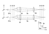
- FIG. 2 is a diagram showing the imaging optical system 5 and the image sensor 40.
- the imaging optical system 5 is an optical system in which the optical axis 5a is bent by the optical path switching member 26.
- the imaging optical system 5 is conceptually shown as a straight optical system.
- the configuration between the objective lens 21 and the cylindrical lens 61 is not shown.
- a direction parallel to the optical axis 5a of the imaging optical system 5 is defined as a Z direction
- two directions perpendicular to the Z direction and perpendicular to each other are defined as an X direction and a Y direction.
- the X direction is, for example, the horizontal direction of the image sensor 40
- the Y direction is, for example, the vertical direction of the image sensor 40.
- the cylindrical lens 61 is an optical member having power (refractive power) only in one of the vertical direction and the horizontal direction.
- the cylindrical lens 61 is described as having power in the XZ plane and not having power in the YZ plane.
- the astigmatism optical system may use a toroidal lens having power in both the vertical direction and the horizontal direction and having different powers in these two directions instead of the cylindrical lens 61.
- FIG. 3 is a diagram showing an optical path of fluorescence and an image of fluorescence from the position Z2 in the sample W.
- the fluorescent light from the fluorescent material present at the position Z2 in the sample W enters the cylindrical lens 61 as parallel light.
- the fluorescence is directed toward the image sensor 40 while being condensed by refraction at the cylindrical lens 61.
- the width Wx of the fluorescent image in the X direction is minimum at a position Z4 corresponding to the focal point on the XZ plane. Further, the width Wx increases as the distance from the position Z4 increases to the side opposite to the sample W (+ Z side).
- the fluorescent light from the fluorescent material present at the position Z2 in the sample W enters the cylindrical lens 61 as parallel light. This fluorescence is incident on the lens 28 without being refracted by the cylindrical lens 61. The fluorescent light is directed toward the image sensor 40 while being condensed by the refraction of the lens 28.
- the width Wy of the fluorescent image in the Y direction is minimum at a position Z6 corresponding to the focal point on the YZ plane. The width Wy increases with distance from the position Z6 to the same side as the sample W ( ⁇ Z side).
- the width Wx of the fluorescence image in the X direction is equal to the width Wy of the fluorescence image in the X direction, and the fluorescence image becomes a perfect circle. Therefore, when the imaging device 40 is arranged at the position Z5, a perfect circle image is acquired as an image of fluorescence from the fluorescent substance existing at the position Z2 in the sample W.
- FIG. 4 is a diagram showing an optical path of fluorescence from the fluorescent substance existing at position Z1 in the sample W and an image of the fluorescence.
- the position Z1 is on the opposite side ( ⁇ Z side) from the image sensor 40 with respect to the position Z2.
- the width Wx of the fluorescence image in the X direction is minimum at a position away from the position Z4 toward the sample W side ( ⁇ Z side).
- the width Wy of the fluorescence image in the Y direction is minimum at the position Z5. Therefore, when the image sensor 40 is arranged at the position Z5, an elliptical image having the major axis in the X direction is acquired as the fluorescence image from the fluorescent substance existing at the position Z1 in the sample W.
- FIG. 5 is a diagram showing an optical path of fluorescence from the fluorescent substance existing at position Z3 in the sample W and an image of fluorescence.
- the position Z3 is on the same side (+ Z side) as the image sensor 40 with respect to the position Z2.
- the width Wx of the fluorescence image in the X direction is minimum at the position Z5.
- the width Wy of the fluorescence image in the Y direction is minimum at a position away from the position Z6 on the side opposite to the sample W (+ Z side). Therefore, when the image sensor 40 is arranged at the position Z5, an elliptical image having the major axis in the Y direction is acquired as an image of fluorescence from the fluorescent substance existing at the position Z3 in the sample W.
- the image processing unit 7 performs elliptic Gaussian fitting, for example, and specifies the width Wx and the width Wy in addition to the center of gravity position of the fluorescence image. Thereby, the image processing unit 7 can specify the position in the XY plane of the fluorescent substance corresponding to the fluorescent image from the position of the center of gravity, and can specify the position in the Z direction based on the relationship between the width Wx and the width Wy. .
- FIG. 6 is a diagram illustrating an example of image processing by the image processing unit 7 at a predetermined imaging position.
- the imaging position is the position of the front focal point of the objective lens 21 in the sample W.
- reference numerals P1 to Pn represent imaging results obtained in a predetermined imaging frame period. Since the fluorescent substance activated with a probability corresponding to the intensity of the activation light L2 emits fluorescence when irradiated with the excitation light L1, the number of fluorescent substances corresponding to the probability emits fluorescence in one frame, and between the frames. When seen, fluorescent substances that are different from each other emit fluorescence.
- the image processing unit 7 calculates, for each of the captured images P1 to Pn, the barycentric position of the fluorescent image included in each image and the width in the XY direction.
- the image processing unit 7 calculates the XY position of the center of gravity and the widths Wx and Wy, for example, by performing elliptic Gaussian fitting on the distribution of pixel values in this region.
- the image processing unit 7 also specifies the position of the center of gravity in the Z direction with reference to a previously stored table or the like from the relationship between the calculated widths Wx and Wy.
- the image processing unit 7 calculates the centroid position Q of the fluorescence image Im, and at least a part of the plurality of centroid positions Q corresponding to the plurality of fluorescence images included in the plurality of captured images P1 to Pn. Is used to generate the three-dimensional distribution information of the centroid position Q. Further, based on the three-dimensional distribution information, a three-dimensional super-resolution image SP1 is generated and displayed. The super-resolution image SP1 is obtained by reconstructing the three-dimensional structure of the sample W. Note that the three-dimensional distribution information obtained at a predetermined imaging position is referred to as a layer.
- the 3D super-resolution image SP1 is shown as a 3D image that allows the user to specify the viewing direction.
- a projection image SP2 on the XY plane and a projection image SP3 on the XZ plane may be displayed.
- FIG. 7 is an example of the data structure 45 of the three-dimensional distribution information of the gravity center position Q.
- the XYZ coordinates of the centroid position Q are associated with the number for identifying the centroid position Q.
- the luminance B and the widths Wx and Wy may be associated with each other.
- Three-dimensional distribution information according to the configuration is stored in the storage device 43.
- the structure in the thickness direction of the sample W (that is, the optical axis direction 21a of the objective lens) can be reconfigured even when the objective lens 21 is fixed in the optical axis direction. Can do.
- the range in the thickness direction in which the structure can be reconstructed is centered on the imaging position, the depth of field of the imaging optical system 5, the intensity of fluorescence, and imaging. This is limited by the S / N ratio of the element, the focal length of the cylindrical lens 61, and the like.
- the range in the thickness direction in which the structure can be reconstructed is about 300 nm.
- the structure of the sample W is covered over a wide range in the thickness direction by capturing the fluorescent image by the imaging unit 6 while moving the objective lens 21 in the optical axis direction 21a of the objective lens 21 by the driving unit 50. Reconfigure.
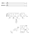
- FIG. 8 is a schematic diagram of an operation sequence of the microscope apparatus 1.
- FIG. 9 is a flowchart showing the imaging process of the microscope apparatus 1.
- FIG. 10 is an example of a screen for inputting imaging conditions in the imaging process.
- the imaging unit 6 performs imaging a plurality of times at a predetermined imaging position as one imaging processing unit. Also, as shown in FIG. 7, the image acquisition procedure at a plurality of predetermined imaging positions is called a pass. Therefore, the path is, for example, that the objective lens 21 moves from the imaging position 1 to the imaging position 8 in the direction of the optical axis 5a of the objective lens 21 and performs imaging.
- an imaging condition is set in the imaging process (S100).
- the microscope apparatus 1 displays a screen 100 as shown in FIG.
- the control device 8 stores, through the screen 100, the position of the lowermost surface of the imaging, the position of the uppermost surface of the imaging, the step size in the Z direction, the number of frames acquired at each imaging position, and the three-dimensional distribution information as the imaging conditions. Accepts input.
- the number of the imaging position and the corresponding number of frames are manually input by the user.
- the number of frames for the imaging position may be automatically calculated based on a predetermined rule. For example, when the density of the stained intracellular tissue is higher in the lower layer of the cell and lower in the upper layer, it is preferable to increase the number of frames as the imaging position is farther from the cover glass 51.
- the imaging order within each pass may be specified.
- the sequential movement from the lower imaging position to the upper imaging position is selected as described above.
- this imaging order it may be possible to select an imaging order such as random, from the top to the bottom, with even-numbered imaging positions first, followed by odd-numbered imaging positions.
- the imaging order of Z1, Z8, Z2, Z7, Z3, Z6, and Z5 can be designated. With this imaging order, an image with a clear sample outline can be obtained.
- the control device 8 calculates an imaging position, that is, a driving amount by the driving unit 50 from the imaging condition (S102).
- an imaging position that is, a driving amount by the driving unit 50 from the imaging condition (S102).
- the imaging position and / or other imaging conditions are set so that a part of the sample W in the thickness direction overlaps between adjacent layers.
- FIG. 8 shows an example of an operation sequence in which the number of layers is 8 and the number of paths is 1.
- the illumination optical system 4 irradiates the sample W1 with the activation light L2 and the excitation light L1 from the light source 3 (S104), and performs imaging by the imaging unit 6 (S106) for a predetermined number of frames corresponding to the imaging position (S108: No). ).
- the control unit 8 determines whether or not the final path has been reached (S111). If the final path has not been reached (S111: No), the process proceeds to the next path, and steps S104 to S110 are repeated. When the final path is reached (S111: Yes), the imaging process ends.
- the sample structure when the sample structure is reconfigured by a method such as STORM, the sample structure is reconfigured in a wider range than the range in the thickness direction limited by the focal length of the cylindrical lens. can do.
- the structure of the sample is reconstructed based on the imaging results of different frames for each imaging position, it is possible to expect an improvement in the image quality of the reconstructed image according to the shape and properties of the sample.
- the image processing unit 7 specifies the center of gravity position of the fluorescence in each imaging frame as described with reference to FIG.
- the image processing unit 7 further stores, in the storage device 43, the three-dimensional distribution information of the centroid position specified in each imaging frame included in the imaging processing unit for each imaging position as a file having the data configuration shown in FIG.
- FIG. 11 is a schematic diagram showing a plurality of layers specified by imaging at a plurality of imaging positions.
- FIG. 11 shows a case where the number of layers is 3 and the number of paths is 1.
- the image processing unit 7 stores the fluorescence gravity center position specified for each path and for each layer, that is, for each photographing processing unit, in the storage device 43 in association with information for identifying the path and the layer.
- the Z position of the center of gravity of each fluorescence in the sample space is the imaging position based on the drive amount of the drive unit 50 and the Z position of the center of gravity of the fluorescence in each layer (Z position of the center of gravity calculated from the captured fluorescence image). And is specified using As described above, the imaging position is the position of the front focal point of the objective lens 21 in the sample, but the position of the front focal point may be a position based on the cover glass 51.
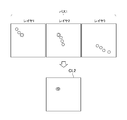
- FIG. 12 is an example of a screen 150 for setting a display image for reconstruction of the sample W.
- the screen 150 is displayed on the display device 44 and accepts the setting of whether to visually distinguish and display the path, the layer, or both.
- FIG. 12 shows an example in which display colors are used as a method of visually distinguishing.
- a path and a layer may be distinguished from each other among three attributes of color, for example, a path is a hue and a layer is a brightness. Thereby, both the path and the layer can be visually distinguished.
- the display color may be visually distinguishable by hatching or shape, for example, a circle, a triangle, or a cross mark.
- the area 152 of the screen 150 is for selecting whether or not to perform color coding for each layer
- the area 154 is for selecting whether or not to perform color coding for each path.
- a state in which the white layers are arranged in the vertical direction is schematically shown, and further on the right side, a state in which the color is classified for each layer when color coding is selected is schematically shown. Is represented.
- a state in which the white paths are arranged in the left-right direction is schematically shown, and further on the right side, a state in which the colors are classified for each pass when color coding is selected is schematically shown. Is represented.
- a box 156 is used to input a lower limit of a range in the Z direction to be displayed, and a box 157 is used to input an upper limit. Further, a box 158 is used to input a lower limit of a path to be displayed, and a box 159 is used to input an upper limit.
- the screen 150 further displays information on the data structure and data range obtained by the photographing process. As the data structure, the layer thickness, the number of layers, and the number of passes are displayed.
- FIG. 13 shows a display image CL1 color-coded for each layer by the setting of FIG. 12 using the three-dimensional distribution information of FIG.
- color cannot be used in the figure, white, hatched, and black are used as a substitute for color.
- the image processing unit 7 calls the fluorescent barycentric position stored in the storage device 43 and assigns a color based on the information for identifying the layer.
- the image processing unit 7 assigns white to the center of gravity of the fluorescence of layer 1, assigns hatching to the center of gravity of the fluorescence of layer 2, assigns black to the center of gravity of the fluorescence of layer 3, and generates a display image CL 1, It is displayed on the display device 44.
- the image processing unit 7 displays which of the plurality of layers belongs to the center of gravity so as to be visually distinguishable, the drift of the objective lens 21 and the stage 2 between layers (for example, The user can easily recognize how much (appears as misalignment).
- FIG. 14 is a schematic diagram showing the overlap in the thickness direction of the sample between layers.
- the plurality of imaging positions are preferably set so that a part of the three-dimensional distribution information generated as a result overlaps in the thickness direction of the sample.
- FIG. 14 shows that there is an overlap Lw between layer 1 and layer 2. Therefore, it is preferable that the setting screen 150 in FIG. 12 can be set to display the center of gravity position included in the overlap Lw manually or automatically.
- FIG. 15 is a schematic diagram illustrating a display image CL2 that displays the position of the center of gravity included in the overlap Lw.
- the image processing unit 7 specifies the barycentric position having the Z coordinate included in the overlap Lw from the three-dimensional distribution information of each layer. In the example illustrated in FIG. 15, it is specified that the barycentric positions surrounded by the broken lines in Layer 1 and Layer 2 are included in the overlap Lw.
- the image processing unit 7 assigns white to the barycentric position in layer 1 and assigns hatching to the barycentric position in layer 2 to generate a display image CL2 and display it on the display device 44. Thereby, the degree of drift of the objective lens 21 and the stage 2 between layers can be recognized more easily.
- FIG. 16 is a schematic diagram of another operation sequence of the microscope apparatus 1.
- FIG. 17 is an example of a screen 110 for inputting imaging conditions in the imaging processing corresponding to FIG.
- the microscope apparatus 1 repeats the pass multiple times. Specifically, 10 passes from pass 1 to pass 10 are repeated.
- the number of passes is input by the user using the screen 110 in FIG.
- the screen 110 is similar to the screen 100 in FIG. 10, and is the name of the file that stores the position of the lowermost surface of the imaging, the position of the uppermost surface of the imaging, the step size in the Z direction, the imaging order in each path, and the 3D distribution information. Accept input.
- the screen 110 further accepts input of the total number of frames used for each layer.
- step S102 by dividing the total number of frames input from the screen 110 by the number of passes, the number of frames acquired at each imaging position of each path, that is, the number of frames for each imaging processing unit is calculated. For example, when the total number of all passes for each imaging position is 10,000, and the number of passes is 10, the number of frames obtained at each imaging position is 1000. Note that the number of frames may be different for each imaging position, as in the examples of FIGS.
- the operation of sequentially moving the imaging positions 1 to 8 is defined as one pass, and this is repeated 10 times. In other words, it moves to each imaging position by the number of passes, and a frame for the above-mentioned imaging processing unit is imaged at each imaging position.
- the number of imaging frames increases.
- the fluorescent material is faded, and for example, the amount of the fluorescent material may be greatly different between the layer at the first imaging position and the layer at the last imaging position.
- a difference in the amount of fluorescent material due to fading between layers can be reduced, and a difference in image quality between layers can be reduced.
- FIG. 18 is a schematic diagram showing a plurality of layers specified by imaging at a plurality of paths and a plurality of imaging positions.
- FIG. 18 shows a case where the number of layers is 3 and the number of paths is 2.
- FIG. 19 shows a display image CL3 color-coded for each layer using the path of FIG. However, for the same reason as in FIG. 13, white, hatched, and black were used as color substitutes.
- the image processing unit 7 calls the XYZ position of the fluorescent image stored in the storage device 43 and assigns a color based on at least information for identifying the layer.
- the image processing unit 7 assigns white to the fluorescence image of layer 1 included in all paths, assigns hatching to the fluorescence image of layer 2 included in all paths, and applies the fluorescence image of layer 3 included in all paths.
- a display image CL3 to which black is assigned is generated and displayed on the display device 44. In this case, it is preferable to indicate the colors from layer 1 to layer 3 as legends and to indicate that they are not distinguished for each path by a character string “all paths” or the like.
- the image processing unit 7 displays the three-dimensional position specified based on the imaging results of the plurality of layers in a visually distinguishable manner, the imaging time between layers The user can easily recognize how much drift (positional deviation) occurs between the sample W and the objective lens caused by the difference.
- FIG. 20 shows a display image CL4 color-coded for each path using the layers of FIG. However, white and black were used as a substitute for color.
- the image processing unit 7 calls the XYZ position of the fluorescence image stored in the storage device 43 and assigns a color based on at least information for identifying the path.
- the image processing unit 7 assigns white to the fluorescence images of all layers included in pass 1, assigns black to the fluorescence images of all layers included in pass 2, and generates a display image CL4. Is displayed on the display device 44.
- the image processing unit 7 indicates the color of the pass 1 and the color of the pass 2 as a legend, and also indicates that the layers are not distinguished by a character string of “all layers” or the like.
- the image processing unit 7 displays which of the plurality of passes is identified as a three-dimensional position based on the imaging result, the sample W is displayed between the passes. It is possible for the user to easily recognize the degree of drift.
- FIG. 11 FIG. 15, FIG. 18 to FIG. 20, the three-dimensional distribution information is shown as “image”, but this is for explanation. That is, except when displaying as a “display image” on the display device 44, the image processing unit 7 does not have to generate an image, and it is only necessary to handle the data as shown in FIG.
- the imaging unit is moved by the drive unit 50 moving the objective lens 21 in the optical axis direction 5a.
- the drive unit 50 may move the imaging position by moving the stage 2 in the optical axis direction 5 a of the objective lens 21.
- an odd number of paths is irradiated with excitation light having a wavelength that excites one fluorescent material, and a wavelength that excites another fluorescent material in the even number of paths.
- the excitation light may be irradiated.
Landscapes
- Physics & Mathematics (AREA)
- General Physics & Mathematics (AREA)
- Chemical & Material Sciences (AREA)
- Analytical Chemistry (AREA)
- Multimedia (AREA)
- Engineering & Computer Science (AREA)
- Optics & Photonics (AREA)
- Health & Medical Sciences (AREA)
- Computer Vision & Pattern Recognition (AREA)
- Biochemistry (AREA)
- Life Sciences & Earth Sciences (AREA)
- General Health & Medical Sciences (AREA)
- Nuclear Medicine, Radiotherapy & Molecular Imaging (AREA)
- Pathology (AREA)
- Immunology (AREA)
- Signal Processing (AREA)
- Microscoopes, Condenser (AREA)
- Investigating, Analyzing Materials By Fluorescence Or Luminescence (AREA)
- Studio Devices (AREA)
Abstract
Un microscope selon la présente invention comprend : un système optique d'éclairage qui émet une lumière d'activation pour activer une partie d'un matériau fluorescent compris dans un échantillon, et une lumière d'excitation pour exciter au moins une partie du matériau fluorescent activé ; un objectif ; un système optique de formation d'image qui forme une image de fluorescence et qui possède un système optique astigmate qui génère un astigmatisme par rapport à au moins une partie de la fluorescence provenant de la matière fluorescente ; une unité d'imagerie qui capture l'image formée par le système optique de formation d'image ; une unité d'entraînement qui déplace une position d'imagerie dans l'échantillon le long de la direction d'axe optique de l'objectif ; et une unité de commande. L'unité de commande amène l'unité d'imagerie à capturer l'image dans une pluralité de trames à une première position d'imagerie et à une seconde position d'imagerie différente de la première position d'imagerie.
Priority Applications (5)
| Application Number | Priority Date | Filing Date | Title |
|---|---|---|---|
| EP15909328.5A EP3385769A4 (fr) | 2015-11-27 | 2015-11-27 | Microscope |
| JP2017552258A JP6617774B2 (ja) | 2015-11-27 | 2015-11-27 | 顕微鏡装置 |
| PCT/JP2015/083511 WO2017090211A1 (fr) | 2015-11-27 | 2015-11-27 | Microscope |
| US15/991,426 US20180275061A1 (en) | 2015-11-27 | 2018-05-29 | Microscope apparatus |
| US17/178,957 US11906431B2 (en) | 2015-11-27 | 2021-02-18 | Microscope apparatus |
Applications Claiming Priority (1)
| Application Number | Priority Date | Filing Date | Title |
|---|---|---|---|
| PCT/JP2015/083511 WO2017090211A1 (fr) | 2015-11-27 | 2015-11-27 | Microscope |
Related Child Applications (1)
| Application Number | Title | Priority Date | Filing Date |
|---|---|---|---|
| US15/991,426 Continuation US20180275061A1 (en) | 2015-11-27 | 2018-05-29 | Microscope apparatus |
Publications (1)
| Publication Number | Publication Date |
|---|---|
| WO2017090211A1 true WO2017090211A1 (fr) | 2017-06-01 |
Family
ID=58763206
Family Applications (1)
| Application Number | Title | Priority Date | Filing Date |
|---|---|---|---|
| PCT/JP2015/083511 WO2017090211A1 (fr) | 2015-11-27 | 2015-11-27 | Microscope |
Country Status (4)
| Country | Link |
|---|---|
| US (2) | US20180275061A1 (fr) |
| EP (1) | EP3385769A4 (fr) |
| JP (1) | JP6617774B2 (fr) |
| WO (1) | WO2017090211A1 (fr) |
Cited By (1)
| Publication number | Priority date | Publication date | Assignee | Title |
|---|---|---|---|---|
| WO2022062084A1 (fr) * | 2020-09-23 | 2022-03-31 | 诚瑞光学(深圳)有限公司 | Dispositif d'acquisition d'image |
Families Citing this family (1)
| Publication number | Priority date | Publication date | Assignee | Title |
|---|---|---|---|---|
| JP7137422B2 (ja) * | 2018-09-28 | 2022-09-14 | シスメックス株式会社 | 顕微鏡装置 |
Citations (7)
| Publication number | Priority date | Publication date | Assignee | Title |
|---|---|---|---|---|
| US20080182336A1 (en) | 2006-08-07 | 2008-07-31 | President And Fellows Of Harvard College | Sub-diffraction limit image resolution and other imaging techniques |
| JP2011508214A (ja) * | 2007-12-21 | 2011-03-10 | プレジデント アンド フェロウズ オブ ハーバード カレッジ | 三次元の回折限界未満の画像解像技術 |
| WO2011152523A1 (fr) * | 2010-06-03 | 2011-12-08 | 株式会社ニコン | Dispositif de microscope |
| JP2013015665A (ja) * | 2011-07-04 | 2013-01-24 | Nikon Corp | 顕微鏡装置及び画像形成方法 |
| JP2014089311A (ja) * | 2012-10-30 | 2014-05-15 | Nikon Corp | 顕微鏡装置及び画像形成方法 |
| JP2015502566A (ja) * | 2011-10-25 | 2015-01-22 | サンフォード−バーナム メディカル リサーチ インスティテュート | 自動化された顕微鏡使用のための多関数型自動焦点システムおよび方法 |
| JP2015506498A (ja) * | 2012-01-11 | 2015-03-02 | カール ツァイス マイクロスコピー ゲーエムベーハーCarl Zeiss Microscopy Gmbh | 高分解能3d蛍光顕微鏡法のための顕微鏡および方法 |
Family Cites Families (10)
| Publication number | Priority date | Publication date | Assignee | Title |
|---|---|---|---|---|
| JP4468684B2 (ja) | 2003-12-05 | 2010-05-26 | オリンパス株式会社 | 走査型共焦点顕微鏡装置 |
| JP4996319B2 (ja) | 2007-04-26 | 2012-08-08 | オリンパス株式会社 | レーザ顕微鏡とその画像表示方法 |
| EP2157466A4 (fr) | 2007-06-15 | 2012-05-09 | Nikon Corp | Dispositif de microscope confocal |
| DE102009060793A1 (de) * | 2009-12-22 | 2011-07-28 | Carl Zeiss Microlmaging GmbH, 07745 | Hochauflösendes Mikroskop und Verfahren zur zwei- oder dreidimensionalen Positionsbestimmung von Objekten |
| US9946058B2 (en) * | 2010-06-11 | 2018-04-17 | Nikon Corporation | Microscope apparatus and observation method |
| EP2966492B1 (fr) * | 2012-05-02 | 2020-10-21 | Centre National De La Recherche Scientifique | Procédé et appareil de localisation de particules uniques au moyen d'une analyse d'ondelettes |
| US8818117B2 (en) | 2012-07-19 | 2014-08-26 | Sony Corporation | Method and apparatus for compressing Z-stack microscopy images |
| US10429628B2 (en) * | 2015-04-23 | 2019-10-01 | The University Of British Columbia | Multifocal method and apparatus for stabilization of optical systems |
| US20180329225A1 (en) * | 2015-08-31 | 2018-11-15 | President And Fellows Of Harvard College | Pattern Detection at Low Signal-To-Noise Ratio |
| JP6635125B2 (ja) | 2015-11-27 | 2020-01-22 | 株式会社ニコン | 顕微鏡、観察方法、及び画像処理プログラム |
-
2015
- 2015-11-27 EP EP15909328.5A patent/EP3385769A4/fr not_active Withdrawn
- 2015-11-27 WO PCT/JP2015/083511 patent/WO2017090211A1/fr active Application Filing
- 2015-11-27 JP JP2017552258A patent/JP6617774B2/ja active Active
-
2018
- 2018-05-29 US US15/991,426 patent/US20180275061A1/en not_active Abandoned
-
2021
- 2021-02-18 US US17/178,957 patent/US11906431B2/en active Active
Patent Citations (7)
| Publication number | Priority date | Publication date | Assignee | Title |
|---|---|---|---|---|
| US20080182336A1 (en) | 2006-08-07 | 2008-07-31 | President And Fellows Of Harvard College | Sub-diffraction limit image resolution and other imaging techniques |
| JP2011508214A (ja) * | 2007-12-21 | 2011-03-10 | プレジデント アンド フェロウズ オブ ハーバード カレッジ | 三次元の回折限界未満の画像解像技術 |
| WO2011152523A1 (fr) * | 2010-06-03 | 2011-12-08 | 株式会社ニコン | Dispositif de microscope |
| JP2013015665A (ja) * | 2011-07-04 | 2013-01-24 | Nikon Corp | 顕微鏡装置及び画像形成方法 |
| JP2015502566A (ja) * | 2011-10-25 | 2015-01-22 | サンフォード−バーナム メディカル リサーチ インスティテュート | 自動化された顕微鏡使用のための多関数型自動焦点システムおよび方法 |
| JP2015506498A (ja) * | 2012-01-11 | 2015-03-02 | カール ツァイス マイクロスコピー ゲーエムベーハーCarl Zeiss Microscopy Gmbh | 高分解能3d蛍光顕微鏡法のための顕微鏡および方法 |
| JP2014089311A (ja) * | 2012-10-30 | 2014-05-15 | Nikon Corp | 顕微鏡装置及び画像形成方法 |
Non-Patent Citations (1)
| Title |
|---|
| See also references of EP3385769A4 |
Cited By (1)
| Publication number | Priority date | Publication date | Assignee | Title |
|---|---|---|---|---|
| WO2022062084A1 (fr) * | 2020-09-23 | 2022-03-31 | 诚瑞光学(深圳)有限公司 | Dispositif d'acquisition d'image |
Also Published As
| Publication number | Publication date |
|---|---|
| JP6617774B2 (ja) | 2019-12-11 |
| EP3385769A4 (fr) | 2019-10-30 |
| EP3385769A1 (fr) | 2018-10-10 |
| US20210172877A1 (en) | 2021-06-10 |
| JPWO2017090211A1 (ja) | 2018-09-06 |
| US20180275061A1 (en) | 2018-09-27 |
| US11906431B2 (en) | 2024-02-20 |
Similar Documents
| Publication | Publication Date | Title |
|---|---|---|
| US10768402B2 (en) | Microscopy of a tissue sample using structured illumination | |
| JP7424286B2 (ja) | 蛍光観察装置及び蛍光観察方法 | |
| JP5485156B2 (ja) | 顕微鏡により試料を3次元結像するための方法 | |
| JP2015135463A (ja) | 顕微鏡装置、及び、顕微鏡システム | |
| WO2018116851A1 (fr) | Dispositif de traitement d'informations, dispositif de traitement d'image, microscope, procédé et programme de traitement d'informations | |
| JP6587004B2 (ja) | 装置、システム、方法、及びプログラム | |
| WO2009139058A1 (fr) | Dispositif d'imagerie biologique | |
| CN104122662B (zh) | 一种超高密度超分辨光学闪烁显微成像系统及方法 | |
| CA2865922A1 (fr) | Scanner avec une plage dynamique accrue | |
| JP2012237693A (ja) | 画像処理装置、画像処理方法及び画像処理プログラム | |
| US10725278B2 (en) | Microscope, observation method, and storage medium | |
| US11906431B2 (en) | Microscope apparatus | |
| JP2006171024A (ja) | 多点蛍光分光測光顕微鏡および多点蛍光分光測光方法 | |
| US20120140057A1 (en) | Microscope for Measuring Total Reflection Fluorescence | |
| JP6253509B2 (ja) | 画像表示方法、制御装置、顕微鏡システム | |
| JP6928757B2 (ja) | 光学顕微鏡における画像処理のためのシステムおよび方法 | |
| WO2016157345A1 (fr) | Dispositif de microscope, procédé de visualisation et programme de commande | |
| JP2020042283A (ja) | 顕微鏡装置 | |
| WO2012144515A1 (fr) | Dispositif de microscope et procédé de traitement d'image | |
| WO2015194410A1 (fr) | Dispositif d'entrée d'image et dispositif microscope | |
| JP2004177732A (ja) | 光学測定装置 | |
| WO2023189393A1 (fr) | Système d'observation d'échantillon biologique, dispositif de traitement d'informations et procédé de génération d'image | |
| JP2018161081A (ja) | 細胞観察装置および細胞観察方法 | |
| JP2008224364A (ja) | 位相情報検出方法及び位相情報検出装置 |
Legal Events
| Date | Code | Title | Description |
|---|---|---|---|
| 121 | Ep: the epo has been informed by wipo that ep was designated in this application |
Ref document number: 15909328 Country of ref document: EP Kind code of ref document: A1 |
|
| ENP | Entry into the national phase |
Ref document number: 2017552258 Country of ref document: JP Kind code of ref document: A |
|
| NENP | Non-entry into the national phase |
Ref country code: DE |
|
| WWE | Wipo information: entry into national phase |
Ref document number: 2015909328 Country of ref document: EP |