WO2017090211A1 - Microscope apparatus - Google Patents
Microscope apparatus Download PDFInfo
- Publication number
- WO2017090211A1 WO2017090211A1 PCT/JP2015/083511 JP2015083511W WO2017090211A1 WO 2017090211 A1 WO2017090211 A1 WO 2017090211A1 JP 2015083511 W JP2015083511 W JP 2015083511W WO 2017090211 A1 WO2017090211 A1 WO 2017090211A1
- Authority
- WO
- WIPO (PCT)
- Prior art keywords
- imaging
- imaging position
- image
- optical system
- dimensional image
- Prior art date
Links
- 238000003384 imaging method Methods 0.000 claims abstract description 271
- 230000003287 optical effect Effects 0.000 claims abstract description 125
- 230000005284 excitation Effects 0.000 claims abstract description 46
- 239000000463 material Substances 0.000 claims abstract description 29
- 238000005286 illumination Methods 0.000 claims abstract description 21
- 201000009310 astigmatism Diseases 0.000 claims abstract description 16
- 230000003213 activating effect Effects 0.000 claims abstract 4
- 239000000126 substance Substances 0.000 claims description 32
- 238000000034 method Methods 0.000 claims description 27
- 239000003086 colorant Substances 0.000 claims description 9
- 230000004913 activation Effects 0.000 abstract description 41
- 239000000975 dye Substances 0.000 description 23
- 238000010586 diagram Methods 0.000 description 21
- 230000005484 gravity Effects 0.000 description 21
- 238000002073 fluorescence micrograph Methods 0.000 description 18
- 239000012190 activator Substances 0.000 description 7
- 239000006059 cover glass Substances 0.000 description 6
- 239000007850 fluorescent dye Substances 0.000 description 5
- 230000012447 hatching Effects 0.000 description 4
- 238000009825 accumulation Methods 0.000 description 3
- 230000000903 blocking effect Effects 0.000 description 3
- 102000034287 fluorescent proteins Human genes 0.000 description 3
- 108091006047 fluorescent proteins Proteins 0.000 description 3
- 230000004807 localization Effects 0.000 description 3
- 238000000386 microscopy Methods 0.000 description 3
- 238000006243 chemical reaction Methods 0.000 description 2
- ANRHNWWPFJCPAZ-UHFFFAOYSA-M thionine Chemical compound [Cl-].C1=CC(N)=CC2=[S+]C3=CC(N)=CC=C3N=C21 ANRHNWWPFJCPAZ-UHFFFAOYSA-M 0.000 description 2
- WSFSSNUMVMOOMR-UHFFFAOYSA-N Formaldehyde Chemical compound O=C WSFSSNUMVMOOMR-UHFFFAOYSA-N 0.000 description 1
- 230000005540 biological transmission Effects 0.000 description 1
- 238000005562 fading Methods 0.000 description 1
- 239000008098 formaldehyde solution Substances 0.000 description 1
- 230000003834 intracellular effect Effects 0.000 description 1
- 239000004973 liquid crystal related substance Substances 0.000 description 1
- 238000012986 modification Methods 0.000 description 1
- 230000004048 modification Effects 0.000 description 1
- 239000013307 optical fiber Substances 0.000 description 1
- 210000001747 pupil Anatomy 0.000 description 1
- 239000007787 solid Substances 0.000 description 1
Images


Classifications
-
- G—PHYSICS
- G02—OPTICS
- G02B—OPTICAL ELEMENTS, SYSTEMS OR APPARATUS
- G02B21/00—Microscopes
- G02B21/16—Microscopes adapted for ultraviolet illumination ; Fluorescence microscopes
-
- G—PHYSICS
- G01—MEASURING; TESTING
- G01N—INVESTIGATING OR ANALYSING MATERIALS BY DETERMINING THEIR CHEMICAL OR PHYSICAL PROPERTIES
- G01N21/00—Investigating or analysing materials by the use of optical means, i.e. using sub-millimetre waves, infrared, visible or ultraviolet light
- G01N21/62—Systems in which the material investigated is excited whereby it emits light or causes a change in wavelength of the incident light
- G01N21/63—Systems in which the material investigated is excited whereby it emits light or causes a change in wavelength of the incident light optically excited
- G01N21/64—Fluorescence; Phosphorescence
- G01N21/645—Specially adapted constructive features of fluorimeters
- G01N21/6456—Spatial resolved fluorescence measurements; Imaging
- G01N21/6458—Fluorescence microscopy
-
- G—PHYSICS
- G01—MEASURING; TESTING
- G01N—INVESTIGATING OR ANALYSING MATERIALS BY DETERMINING THEIR CHEMICAL OR PHYSICAL PROPERTIES
- G01N21/00—Investigating or analysing materials by the use of optical means, i.e. using sub-millimetre waves, infrared, visible or ultraviolet light
- G01N21/62—Systems in which the material investigated is excited whereby it emits light or causes a change in wavelength of the incident light
- G01N21/63—Systems in which the material investigated is excited whereby it emits light or causes a change in wavelength of the incident light optically excited
- G01N21/64—Fluorescence; Phosphorescence
-
- G—PHYSICS
- G02—OPTICS
- G02B—OPTICAL ELEMENTS, SYSTEMS OR APPARATUS
- G02B21/00—Microscopes
- G02B21/0004—Microscopes specially adapted for specific applications
- G02B21/002—Scanning microscopes
- G02B21/0024—Confocal scanning microscopes (CSOMs) or confocal "macroscopes"; Accessories which are not restricted to use with CSOMs, e.g. sample holders
- G02B21/0052—Optical details of the image generation
- G02B21/0076—Optical details of the image generation arrangements using fluorescence or luminescence
-
- G—PHYSICS
- G02—OPTICS
- G02B—OPTICAL ELEMENTS, SYSTEMS OR APPARATUS
- G02B21/00—Microscopes
- G02B21/36—Microscopes arranged for photographic purposes or projection purposes or digital imaging or video purposes including associated control and data processing arrangements
- G02B21/365—Control or image processing arrangements for digital or video microscopes
- G02B21/367—Control or image processing arrangements for digital or video microscopes providing an output produced by processing a plurality of individual source images, e.g. image tiling, montage, composite images, depth sectioning, image comparison
-
- H—ELECTRICITY
- H04—ELECTRIC COMMUNICATION TECHNIQUE
- H04N—PICTORIAL COMMUNICATION, e.g. TELEVISION
- H04N23/00—Cameras or camera modules comprising electronic image sensors; Control thereof
-
- G—PHYSICS
- G01—MEASURING; TESTING
- G01N—INVESTIGATING OR ANALYSING MATERIALS BY DETERMINING THEIR CHEMICAL OR PHYSICAL PROPERTIES
- G01N2201/00—Features of devices classified in G01N21/00
- G01N2201/06—Illumination; Optics
- G01N2201/061—Sources
- G01N2201/06113—Coherent sources; lasers
Definitions
- the present invention relates to a microscope apparatus, an imaging method, and a program.
- Patent Document 1 US Patent Application Publication No. 2008/0182336
- an activation light that activates a part of the fluorescent substance contained in the sample, and an illumination optical system that emits excitation light that excites at least a part of the activated fluorescent substance
- An imaging optical system having an objective lens and an astigmatism optical system for generating astigmatism with respect to at least a part of the fluorescence from the fluorescent material, and an imaging optical system
- a microscope having an imaging unit that captures the captured image, a drive unit that moves the imaging position of the sample along the optical axis direction of the objective lens, and a control unit, wherein the control unit includes a first Imaging is performed with a plurality of frames at a second imaging position different from the imaging position and the first imaging position.
- an activation light that activates a part of the fluorescent substance contained in the sample, and an illumination optical system that emits excitation light that excites at least a part of the activated fluorescent substance;
- An imaging optical system having an objective lens and an astigmatism optical system for generating astigmatism with respect to at least a part of the fluorescence from the fluorescent material, and an imaging optical system
- the imaging unit includes a first imaging position and a first imaging position.
- An imaging method is provided in which imaging is performed with a plurality of frames at different second imaging positions.
- an activation light that activates a part of the fluorescent substance contained in the sample, and an illumination optical system that emits excitation light that excites at least a part of the activated fluorescent substance;
- An imaging optical system having an objective lens and an astigmatism optical system for generating astigmatism with respect to at least a part of the fluorescence from the fluorescent material, and an imaging optical system
- a computer that controls a microscope apparatus having an imaging unit that captures the captured image and a drive unit that moves the imaging position of the sample along the optical axis direction of the objective lens, and the imaging unit includes the first imaging position and the first imaging position.
- FIG. 4 is a diagram illustrating an optical path of fluorescence and an image of fluorescence from a position Z2 on a sample W.
- FIG. 4 is a diagram showing an optical path of fluorescence from a fluorescent substance present at position Z1 in a sample W and an image of fluorescence.
- FIG. 3 is a diagram showing an optical path of fluorescence from a fluorescent substance existing at position Z3 in a sample W and an image of fluorescence. It is a figure which shows an example of the image process by the image process part.
- FIG. 4 is a schematic diagram of an operation sequence of the microscope apparatus 1.
- FIG. 4 is a flowchart showing an imaging process of the microscope apparatus 1. It is an example of the screen which inputs the imaging condition in an imaging process. It is a schematic diagram which shows the three-dimensional distribution information of the gravity center position of fluorescence. It is an example of the screen 150 which sets the display image of the reconstruction of the sample W. The display image CL1 color-coded for each layer is shown. It is a schematic diagram which shows the overlap of the thickness direction of the sample between layers. It is a schematic diagram explaining the display image CL2 which displays the gravity center position contained in the overlap Lw.
- FIG. 4 is a flowchart showing an imaging process of the microscope apparatus 1. It is an example of the screen which inputs the imaging condition in an imaging process. It is a schematic diagram which shows the three-dimensional distribution information of the gravity center position of fluorescence. It is an example of the screen 150 which sets the display image of the reconstruction of the sample W. The display image CL1 color-coded for each
- FIG. 6 is a schematic diagram of another operation sequence of the microscope apparatus 1. It is another example of the screen which inputs the imaging condition in an imaging process. It is a schematic diagram which shows the three-dimensional distribution information of the gravity center position of fluorescence.
- the display image CL3 color-coded for each layer is shown.
- the display image CL4 color-coded for each pass is shown.
- the microscope apparatus according to the embodiment is, for example, a microscope apparatus using Single-molecule Localization Microscopy methods such as STORM and PALM.
- the microscope apparatus according to the present embodiment can generate a three-dimensional super-resolution image.
- the microscope apparatus according to the embodiment can be used for both fluorescence observation of a sample labeled with one kind of fluorescent substance and fluorescence observation of a sample labeled with two or more kinds of fluorescent substances.
- the sample may include living cells (live cells), may include cells fixed using a tissue fixing solution such as a formaldehyde solution, or may be tissue.
- the fluorescent substance may be a fluorescent dye such as a cyanine dye or a fluorescent protein.
- the fluorescent dye includes a reporter dye that emits fluorescence when receiving excitation light in an activated state, which is an activated state.
- the fluorescent dye may include an activator dye that receives activation light and activates the reporter dye. If the fluorescent dye does not contain an activator dye, the reporter dye receives an activation light and becomes activated.
- Fluorescent dyes include, for example, a dye pair in which two kinds of cyanine dyes are combined (eg, Cy3-Cy5 dye pair (Cy3, Cy5 is a registered trademark), Cy2-Cy5 dye pair (Cy2, Cy5 is a registered trademark) , Cy3-Alexa® Fluor647 dye pair (Cy3, Alexa® Fluor is a registered trademark)) and one type of dye (eg, Alexa® Fluor647 (Alexa® Fluor is a registered trademark)).
- the fluorescent protein include PA-GFP and Dronpa.
- FIG. 1 is a diagram showing a microscope apparatus 1 according to the present embodiment.
- the microscope apparatus 1 includes a stage 2, a light source device 3, an illumination optical system 4, an imaging optical system 5, an imaging unit 6, an image processing unit 7, and a control device 8.
- the control device 8 includes a control unit 42 that comprehensively controls each unit of the microscope apparatus 1.
- the control device 8 may be a computer that executes a procedure to be described later by reading a software program.
- Stage 2 holds a cover glass 51.
- the cover glass 51 holds the sample W to be observed. More specifically, as shown in FIG. 1, the cover glass 51 is placed on the stage 2, and the sample W is placed on the cover glass 51.
- the stage 2 may or may not move in the XY plane.
- the light source device 3 includes an activation light source 10a, an excitation light source 10b, a shutter 11a, and a shutter 11b.
- the activation light source 10a emits activation light L2 that activates a part of the fluorescent substance contained in the sample W.
- the fluorescent material contains a reporter dye and does not contain an activator dye.
- the reporter dye of the fluorescent substance is in an activated state capable of emitting fluorescence when irradiated with the activation light L2.
- the fluorescent material may include a reporter dye and an activator dye. In this case, the activator dye activates the reporter dye when receiving the activation light L2.
- the fluorescent substance may be a fluorescent protein such as PA-GFP or Dronpa.
- the excitation light source 10b emits excitation light L1 that excites at least part of the fluorescent material activated in the sample W.
- the fluorescent material emits fluorescence or is inactivated when the excitation light L1 is irradiated in the activated state.
- an inactivated state When the fluorescent material is irradiated with the activation light L2 in an inactivated state (hereinafter referred to as an inactivated state), the fluorescent material is again activated.
- the activation light source 10a and the excitation light source 10b include, for example, a solid light source such as a laser light source, and each emits laser light having a wavelength corresponding to the type of fluorescent material.
- the emission wavelength of the activation light source 10a and the emission wavelength of the excitation light source 10b are selected from, for example, about 405 nm, about 457 nm, about 488 nm, about 532 nm, about 561 nm, about 640 nm, and about 647 nm.
- the emission wavelength of the activation light source 10a is about 405 nm and the emission wavelength of the excitation light source 10b is a wavelength selected from about 488 nm, about 561 nm, and about 647 nm.
- the shutter 11a is controlled by the control unit 42, and can switch between a state in which the activation light L2 from the activation light source 10a passes and a state in which the activation light L2 is blocked.
- the shutter 11b is controlled by the control unit 42 and can switch between a state in which the excitation light L1 from the excitation light source 10b passes and a state in which the excitation light L1 is blocked.
- the light source device 3 includes a mirror 12, a dichroic mirror 13, an acoustooptic device 14, and a lens 15.
- the mirror 12 is provided, for example, on the emission side of the excitation light source 10b. Excitation light L 1 from the excitation light source 10 b is reflected by the mirror 12 and enters the dichroic mirror 13.
- the dichroic mirror 13 is provided, for example, on the emission side of the activation light source 10a.
- the dichroic mirror 13 has a characteristic of transmitting the activation light L2 and reflecting the excitation light L1.
- the activation light L2 transmitted through the dichroic mirror 13 and the excitation light L1 reflected by the dichroic mirror 13 enter the acoustooptic device 14 through the same optical path.
- the acoustooptic element 14 is, for example, an acoustooptic filter.
- the acoustooptic device 14 is controlled by the control unit 42 and can adjust the light intensity of the activation light L2 and the light intensity of the excitation light L1.
- the acoustooptic device 14 is controlled by the control unit 42, and for each of the activation light L ⁇ b> 2 and the excitation light L ⁇ b> 1, a light passing state that is a state that passes through the acoustooptic device 14 and a state that is blocked by the acoustooptic device 14 or It is possible to switch between a light-shielding state in which the intensity is reduced.
- the control unit 42 controls the acoustooptic device 14 so that the activation light L2 and the excitation light L1 are simultaneously irradiated onto the sample W.
- the control unit 42 controls the acoustooptic device 14 such that the excitation light L1 is irradiated on the sample W after irradiation with the activation light L2, for example.
- the lens 15 is a coupler, for example, and collects the activation light L2 and the excitation light L1 from the acoustooptic device 14 on the light guide member 16.
- the microscope apparatus 1 may not include at least a part of the light source device 3.
- the light source device 3 is unitized and may be provided in the microscope device 1 so as to be replaceable (attachable and removable).
- the light source device 3 may be attached to the microscope device 1 during observation with the microscope device 1 or the like.
- the illumination optical system 4 irradiates activation light L2 that activates a part of the fluorescent substance contained in the sample W and excitation light L1 that excites at least a part of the activated fluorescent substance.
- the illumination optical system 4 irradiates the sample W with the activation light L2 and the excitation light L1 from the light source device 3.
- the illumination optical system 4 includes a light guide member 16, a lens 17, a lens 18, a filter 19, a dichroic mirror 20, and an objective lens 21.
- the light guide member 16 is an optical fiber, for example, and guides the activation light L2 and the excitation light L1 to the lens 17.
- the lens 17 is a collimator, for example, and converts the activation light L2 and the excitation light L1 into parallel light.
- the lens 18 condenses the activation light L ⁇ b> 2 and the excitation light L ⁇ b> 1 at the position of the pupil plane of the objective lens 21.
- the filter 19 has a characteristic of transmitting the activation light L2 and the excitation light L1 and blocking at least part of light of other wavelengths.
- the dichroic mirror 20 has a characteristic of reflecting the activation light L2 and the excitation light L1 and transmitting light in the fluorescent wavelength band emitted from the fluorescent material of the sample W.
- the light from the filter 19 is reflected by the dichroic mirror 20 and enters the objective lens 21.
- the sample W is disposed on the front focal plane of the objective lens 21 during observation.
- the activation light L2 and the excitation light L1 are applied to the sample W by the illumination optical system 4 as described above.
- the illumination optical system 4 mentioned above is an example, and can be changed suitably.
- a part of the illumination optical system 4 described above may be omitted.
- the illumination optical system 4 may include at least a part of the light source device 3.
- the illumination optical system 4 may include an aperture stop, an illumination field stop, and the like.
- the imaging optical system 5 forms an image of fluorescence from the fluorescent material contained in the sample W.
- the imaging optical system 5 includes a first optical system 5A that forms a primary image of the fluorescence emitted from the sample W, and a fluorescence as a secondary image in the imaging unit 6 from the primary image generated in the first optical system 5A.
- the first optical system 5A includes an objective lens 21, a dichroic mirror 20, a filter 24, a lens 25, and an optical path switching member 26.
- the second optical system 5B includes a lens 27, a lens 28, and a cylindrical lens 61 as an astigmatism optical system.
- the imaging optical system 5 shares the objective lens 21 and the dichroic mirror 20 with the illumination optical system 4.
- the optical path between the sample W and the imaging unit 6 is indicated by a solid line.
- the drive unit 50 moves the objective lens 21 in the optical axis direction of the objective lens 21, that is, the Z direction in FIG.
- the filter 24 has a characteristic that light in a predetermined wavelength band out of the light from the sample W selectively passes.
- the filter 24 blocks illumination light, external light, stray light, and the like reflected from the sample W.
- the filter 24 is unitized with, for example, the filter 19 and the dichroic mirror 20, and the filter unit 29 is provided in a replaceable manner.
- the filter unit 29 is exchanged according to, for example, the wavelength of light emitted from the light source device 3 (for example, the wavelength of the activation light L2, the wavelength of the excitation light L1), the wavelength of fluorescence emitted from the sample W, and the like.
- a single filter unit corresponding to a plurality of excitation and fluorescence wavelengths may be used.
- the light that has passed through the filter 24 enters the optical path switching member 26 through the lens 25.
- the light emitted from the lens 25 passes through the optical path switching member 26 and then forms a primary image on the intermediate image plane 5b.
- the optical path switching member 26 is a prism, for example, and is provided so as to be insertable into and removable from the optical path of the imaging optical system 5.
- the optical path switching member 26 is inserted into and removed from the optical path of the imaging optical system 5 by a drive unit (not shown) controlled by the control unit 42, for example.
- the optical path switching member 26 guides the fluorescence from the sample W to the optical path toward the imaging unit 6 by internal reflection when inserted in the optical path of the imaging optical system 5.
- the imaging unit 6 captures an image formed by the imaging optical system 5 (first observation optical system 5).
- the imaging unit 6 includes an imaging element 40 and a control unit 41.
- the image sensor 40 is, for example, a CMOS image sensor, but may be a CCD image sensor or the like.
- the image sensor 40 has, for example, a structure in which a plurality of pixels arranged two-dimensionally and a photoelectric conversion element such as a photodiode is arranged in each pixel.
- the imaging element 40 reads out the electric charge accumulated in the photoelectric conversion element by a readout circuit.
- the image sensor 40 converts the read charges into digital data, and outputs data in a digital format (eg, image data) in which pixel positions and gradation values are associated with each other.
- the control unit 41 operates the imaging element 40 based on a control signal input from the control unit 42 of the control device 8 and outputs captured image data to the control device 8. Further, the control unit 41 outputs a charge accumulation period and a
- the imaging optical system 5 described above is an example and can be changed as appropriate. For example, a part of the imaging optical system 5 described above may be omitted.
- the imaging optical system 5 may include an aperture stop, a field stop, and the like.
- the microscope apparatus 1 includes a second observation optical system 30 used for setting an observation range.
- the second observation optical system 30 includes an objective lens 21, a dichroic mirror 20, a filter 24, a lens 25, a mirror 31, a lens 32, a mirror 33, a lens 34, a lens 35, and a mirror in order from the sample W toward the observer's viewpoint Vp. 36 and a lens 37.
- the observation optical system 30 shares the configuration from the objective lens 21 to the lens 25 with the imaging optical system 5.
- the light from the sample W passes through the lens 25 and then enters the mirror 31 in a state where the optical path switching member 26 is retracted from the optical path of the imaging optical system 5.
- the light reflected by the mirror 31 is incident on the mirror 33 via the lens 32, is reflected by the mirror 33, and then enters the mirror 36 via the lens 34 and the lens 35.
- the light reflected by the mirror 36 enters the viewpoint Vp through the lens 37.
- the second observation optical system 30 forms an intermediate image of the sample W in the optical path between the lens 35 and the lens 37.
- the lens 37 is an eyepiece, for example, and the observer can set an observation range by observing the intermediate image.
- the control device 8 collectively controls each part of the microscope device 1.
- the control device 8 includes a control unit 42 and an image processing unit 7. Based on the signals indicating the charge accumulation period and the charge read period supplied from the control unit 41, the control unit 42 transmits light from the light source device 3 to the acoustooptic device 14, and the light source device 3. A control signal for switching between a light blocking state for blocking light from the light source is supplied. The acoustooptic device 14 switches between a light transmission state and a light shielding state based on this control signal.
- the control unit 42 controls the acoustooptic device 14 to control a period during which the sample W is irradiated with the activation light L2 and a period during which the sample W is not irradiated with the activation light L2. Further, the control unit 42 controls the acoustooptic device 14 to control a period during which the sample W is irradiated with the excitation light L1 and a period during which the sample W is not irradiated with the excitation light L1. The control unit 42 controls the acoustooptic device 14 to control the light intensity of the activation light L2 and the light intensity of the excitation light L1 that are irradiated on the sample W. The control unit 42 controls the imaging unit 6 and causes the imaging device 40 to perform imaging.
- control unit 41 controls the acoustooptic device 14 to switch between the light shielding state and the light passing state based on a signal indicating the charge accumulation period and the charge readout period (information on imaging timing).
- a signal may be supplied to control the acousto-optic element 14.
- the control unit 42 acquires data as an imaging result from the imaging unit 6.
- the image processing unit 7 performs image processing such as obtaining the position of the center of gravity of each image using the imaging result of the imaging unit 6.
- the control unit 42 causes the imaging unit 6 to capture images in a plurality of frame periods, and the image processing unit 7 generates one image using at least a part of the imaging results obtained in the plurality of frame periods.
- the control device 8 is connected to, for example, each of the storage device 43 and the display device 44 so as to be communicable.
- the display device 44 is, for example, a liquid crystal display.
- the display device 44 displays various images such as an image indicating various settings of the microscope device 1, a captured image by the imaging unit 6, and an image generated from the captured image.
- the control unit 42 controls the display device 44 to display various images on the display device 44.
- the control unit 42 supplies super display image data such as a STORM image or a PALM image generated by the image processing unit 7 to the display device 44 and causes the display device 44 to display the image.
- the microscope apparatus 1 can also display a super-resolution image of the sample W to be observed as a live video.
- the storage device 43 is, for example, a magnetic disk or an optical disk, and stores various data such as various setting data of the microscope apparatus 1, data of an imaging result by the imaging unit 6, and image data generated by the image processing unit 7.
- the control unit 42 can supply the display device 44 with the data of the super-resolution image stored in the storage device 43 and cause the display device 44 to display the super-resolution image.
- the control unit 42 controls the storage device 43 and stores various data in the storage device 43.
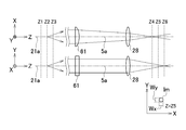
- FIG. 2 is a diagram showing the imaging optical system 5 and the image sensor 40.
- the imaging optical system 5 is an optical system in which the optical axis 5a is bent by the optical path switching member 26.
- the imaging optical system 5 is conceptually shown as a straight optical system.
- the configuration between the objective lens 21 and the cylindrical lens 61 is not shown.
- a direction parallel to the optical axis 5a of the imaging optical system 5 is defined as a Z direction
- two directions perpendicular to the Z direction and perpendicular to each other are defined as an X direction and a Y direction.
- the X direction is, for example, the horizontal direction of the image sensor 40
- the Y direction is, for example, the vertical direction of the image sensor 40.
- the cylindrical lens 61 is an optical member having power (refractive power) only in one of the vertical direction and the horizontal direction.
- the cylindrical lens 61 is described as having power in the XZ plane and not having power in the YZ plane.
- the astigmatism optical system may use a toroidal lens having power in both the vertical direction and the horizontal direction and having different powers in these two directions instead of the cylindrical lens 61.
- FIG. 3 is a diagram showing an optical path of fluorescence and an image of fluorescence from the position Z2 in the sample W.
- the fluorescent light from the fluorescent material present at the position Z2 in the sample W enters the cylindrical lens 61 as parallel light.
- the fluorescence is directed toward the image sensor 40 while being condensed by refraction at the cylindrical lens 61.
- the width Wx of the fluorescent image in the X direction is minimum at a position Z4 corresponding to the focal point on the XZ plane. Further, the width Wx increases as the distance from the position Z4 increases to the side opposite to the sample W (+ Z side).
- the fluorescent light from the fluorescent material present at the position Z2 in the sample W enters the cylindrical lens 61 as parallel light. This fluorescence is incident on the lens 28 without being refracted by the cylindrical lens 61. The fluorescent light is directed toward the image sensor 40 while being condensed by the refraction of the lens 28.
- the width Wy of the fluorescent image in the Y direction is minimum at a position Z6 corresponding to the focal point on the YZ plane. The width Wy increases with distance from the position Z6 to the same side as the sample W ( ⁇ Z side).
- the width Wx of the fluorescence image in the X direction is equal to the width Wy of the fluorescence image in the X direction, and the fluorescence image becomes a perfect circle. Therefore, when the imaging device 40 is arranged at the position Z5, a perfect circle image is acquired as an image of fluorescence from the fluorescent substance existing at the position Z2 in the sample W.
- FIG. 4 is a diagram showing an optical path of fluorescence from the fluorescent substance existing at position Z1 in the sample W and an image of the fluorescence.
- the position Z1 is on the opposite side ( ⁇ Z side) from the image sensor 40 with respect to the position Z2.
- the width Wx of the fluorescence image in the X direction is minimum at a position away from the position Z4 toward the sample W side ( ⁇ Z side).
- the width Wy of the fluorescence image in the Y direction is minimum at the position Z5. Therefore, when the image sensor 40 is arranged at the position Z5, an elliptical image having the major axis in the X direction is acquired as the fluorescence image from the fluorescent substance existing at the position Z1 in the sample W.
- FIG. 5 is a diagram showing an optical path of fluorescence from the fluorescent substance existing at position Z3 in the sample W and an image of fluorescence.
- the position Z3 is on the same side (+ Z side) as the image sensor 40 with respect to the position Z2.
- the width Wx of the fluorescence image in the X direction is minimum at the position Z5.
- the width Wy of the fluorescence image in the Y direction is minimum at a position away from the position Z6 on the side opposite to the sample W (+ Z side). Therefore, when the image sensor 40 is arranged at the position Z5, an elliptical image having the major axis in the Y direction is acquired as an image of fluorescence from the fluorescent substance existing at the position Z3 in the sample W.
- the image processing unit 7 performs elliptic Gaussian fitting, for example, and specifies the width Wx and the width Wy in addition to the center of gravity position of the fluorescence image. Thereby, the image processing unit 7 can specify the position in the XY plane of the fluorescent substance corresponding to the fluorescent image from the position of the center of gravity, and can specify the position in the Z direction based on the relationship between the width Wx and the width Wy. .
- FIG. 6 is a diagram illustrating an example of image processing by the image processing unit 7 at a predetermined imaging position.
- the imaging position is the position of the front focal point of the objective lens 21 in the sample W.
- reference numerals P1 to Pn represent imaging results obtained in a predetermined imaging frame period. Since the fluorescent substance activated with a probability corresponding to the intensity of the activation light L2 emits fluorescence when irradiated with the excitation light L1, the number of fluorescent substances corresponding to the probability emits fluorescence in one frame, and between the frames. When seen, fluorescent substances that are different from each other emit fluorescence.
- the image processing unit 7 calculates, for each of the captured images P1 to Pn, the barycentric position of the fluorescent image included in each image and the width in the XY direction.
- the image processing unit 7 calculates the XY position of the center of gravity and the widths Wx and Wy, for example, by performing elliptic Gaussian fitting on the distribution of pixel values in this region.
- the image processing unit 7 also specifies the position of the center of gravity in the Z direction with reference to a previously stored table or the like from the relationship between the calculated widths Wx and Wy.
- the image processing unit 7 calculates the centroid position Q of the fluorescence image Im, and at least a part of the plurality of centroid positions Q corresponding to the plurality of fluorescence images included in the plurality of captured images P1 to Pn. Is used to generate the three-dimensional distribution information of the centroid position Q. Further, based on the three-dimensional distribution information, a three-dimensional super-resolution image SP1 is generated and displayed. The super-resolution image SP1 is obtained by reconstructing the three-dimensional structure of the sample W. Note that the three-dimensional distribution information obtained at a predetermined imaging position is referred to as a layer.
- the 3D super-resolution image SP1 is shown as a 3D image that allows the user to specify the viewing direction.
- a projection image SP2 on the XY plane and a projection image SP3 on the XZ plane may be displayed.
- FIG. 7 is an example of the data structure 45 of the three-dimensional distribution information of the gravity center position Q.
- the XYZ coordinates of the centroid position Q are associated with the number for identifying the centroid position Q.
- the luminance B and the widths Wx and Wy may be associated with each other.
- Three-dimensional distribution information according to the configuration is stored in the storage device 43.
- the structure in the thickness direction of the sample W (that is, the optical axis direction 21a of the objective lens) can be reconfigured even when the objective lens 21 is fixed in the optical axis direction. Can do.
- the range in the thickness direction in which the structure can be reconstructed is centered on the imaging position, the depth of field of the imaging optical system 5, the intensity of fluorescence, and imaging. This is limited by the S / N ratio of the element, the focal length of the cylindrical lens 61, and the like.
- the range in the thickness direction in which the structure can be reconstructed is about 300 nm.
- the structure of the sample W is covered over a wide range in the thickness direction by capturing the fluorescent image by the imaging unit 6 while moving the objective lens 21 in the optical axis direction 21a of the objective lens 21 by the driving unit 50. Reconfigure.
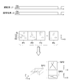
- FIG. 8 is a schematic diagram of an operation sequence of the microscope apparatus 1.
- FIG. 9 is a flowchart showing the imaging process of the microscope apparatus 1.
- FIG. 10 is an example of a screen for inputting imaging conditions in the imaging process.
- the imaging unit 6 performs imaging a plurality of times at a predetermined imaging position as one imaging processing unit. Also, as shown in FIG. 7, the image acquisition procedure at a plurality of predetermined imaging positions is called a pass. Therefore, the path is, for example, that the objective lens 21 moves from the imaging position 1 to the imaging position 8 in the direction of the optical axis 5a of the objective lens 21 and performs imaging.
- an imaging condition is set in the imaging process (S100).
- the microscope apparatus 1 displays a screen 100 as shown in FIG.
- the control device 8 stores, through the screen 100, the position of the lowermost surface of the imaging, the position of the uppermost surface of the imaging, the step size in the Z direction, the number of frames acquired at each imaging position, and the three-dimensional distribution information as the imaging conditions. Accepts input.
- the number of the imaging position and the corresponding number of frames are manually input by the user.
- the number of frames for the imaging position may be automatically calculated based on a predetermined rule. For example, when the density of the stained intracellular tissue is higher in the lower layer of the cell and lower in the upper layer, it is preferable to increase the number of frames as the imaging position is farther from the cover glass 51.
- the imaging order within each pass may be specified.
- the sequential movement from the lower imaging position to the upper imaging position is selected as described above.
- this imaging order it may be possible to select an imaging order such as random, from the top to the bottom, with even-numbered imaging positions first, followed by odd-numbered imaging positions.
- the imaging order of Z1, Z8, Z2, Z7, Z3, Z6, and Z5 can be designated. With this imaging order, an image with a clear sample outline can be obtained.
- the control device 8 calculates an imaging position, that is, a driving amount by the driving unit 50 from the imaging condition (S102).
- an imaging position that is, a driving amount by the driving unit 50 from the imaging condition (S102).
- the imaging position and / or other imaging conditions are set so that a part of the sample W in the thickness direction overlaps between adjacent layers.
- FIG. 8 shows an example of an operation sequence in which the number of layers is 8 and the number of paths is 1.
- the illumination optical system 4 irradiates the sample W1 with the activation light L2 and the excitation light L1 from the light source 3 (S104), and performs imaging by the imaging unit 6 (S106) for a predetermined number of frames corresponding to the imaging position (S108: No). ).
- the control unit 8 determines whether or not the final path has been reached (S111). If the final path has not been reached (S111: No), the process proceeds to the next path, and steps S104 to S110 are repeated. When the final path is reached (S111: Yes), the imaging process ends.
- the sample structure when the sample structure is reconfigured by a method such as STORM, the sample structure is reconfigured in a wider range than the range in the thickness direction limited by the focal length of the cylindrical lens. can do.
- the structure of the sample is reconstructed based on the imaging results of different frames for each imaging position, it is possible to expect an improvement in the image quality of the reconstructed image according to the shape and properties of the sample.
- the image processing unit 7 specifies the center of gravity position of the fluorescence in each imaging frame as described with reference to FIG.
- the image processing unit 7 further stores, in the storage device 43, the three-dimensional distribution information of the centroid position specified in each imaging frame included in the imaging processing unit for each imaging position as a file having the data configuration shown in FIG.
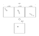
- FIG. 11 is a schematic diagram showing a plurality of layers specified by imaging at a plurality of imaging positions.
- FIG. 11 shows a case where the number of layers is 3 and the number of paths is 1.
- the image processing unit 7 stores the fluorescence gravity center position specified for each path and for each layer, that is, for each photographing processing unit, in the storage device 43 in association with information for identifying the path and the layer.
- the Z position of the center of gravity of each fluorescence in the sample space is the imaging position based on the drive amount of the drive unit 50 and the Z position of the center of gravity of the fluorescence in each layer (Z position of the center of gravity calculated from the captured fluorescence image). And is specified using As described above, the imaging position is the position of the front focal point of the objective lens 21 in the sample, but the position of the front focal point may be a position based on the cover glass 51.
- FIG. 12 is an example of a screen 150 for setting a display image for reconstruction of the sample W.
- the screen 150 is displayed on the display device 44 and accepts the setting of whether to visually distinguish and display the path, the layer, or both.
- FIG. 12 shows an example in which display colors are used as a method of visually distinguishing.
- a path and a layer may be distinguished from each other among three attributes of color, for example, a path is a hue and a layer is a brightness. Thereby, both the path and the layer can be visually distinguished.
- the display color may be visually distinguishable by hatching or shape, for example, a circle, a triangle, or a cross mark.
- the area 152 of the screen 150 is for selecting whether or not to perform color coding for each layer
- the area 154 is for selecting whether or not to perform color coding for each path.
- a state in which the white layers are arranged in the vertical direction is schematically shown, and further on the right side, a state in which the color is classified for each layer when color coding is selected is schematically shown. Is represented.
- a state in which the white paths are arranged in the left-right direction is schematically shown, and further on the right side, a state in which the colors are classified for each pass when color coding is selected is schematically shown. Is represented.
- a box 156 is used to input a lower limit of a range in the Z direction to be displayed, and a box 157 is used to input an upper limit. Further, a box 158 is used to input a lower limit of a path to be displayed, and a box 159 is used to input an upper limit.
- the screen 150 further displays information on the data structure and data range obtained by the photographing process. As the data structure, the layer thickness, the number of layers, and the number of passes are displayed.
- FIG. 13 shows a display image CL1 color-coded for each layer by the setting of FIG. 12 using the three-dimensional distribution information of FIG.
- color cannot be used in the figure, white, hatched, and black are used as a substitute for color.
- the image processing unit 7 calls the fluorescent barycentric position stored in the storage device 43 and assigns a color based on the information for identifying the layer.
- the image processing unit 7 assigns white to the center of gravity of the fluorescence of layer 1, assigns hatching to the center of gravity of the fluorescence of layer 2, assigns black to the center of gravity of the fluorescence of layer 3, and generates a display image CL 1, It is displayed on the display device 44.
- the image processing unit 7 displays which of the plurality of layers belongs to the center of gravity so as to be visually distinguishable, the drift of the objective lens 21 and the stage 2 between layers (for example, The user can easily recognize how much (appears as misalignment).
- FIG. 14 is a schematic diagram showing the overlap in the thickness direction of the sample between layers.
- the plurality of imaging positions are preferably set so that a part of the three-dimensional distribution information generated as a result overlaps in the thickness direction of the sample.
- FIG. 14 shows that there is an overlap Lw between layer 1 and layer 2. Therefore, it is preferable that the setting screen 150 in FIG. 12 can be set to display the center of gravity position included in the overlap Lw manually or automatically.
- FIG. 15 is a schematic diagram illustrating a display image CL2 that displays the position of the center of gravity included in the overlap Lw.
- the image processing unit 7 specifies the barycentric position having the Z coordinate included in the overlap Lw from the three-dimensional distribution information of each layer. In the example illustrated in FIG. 15, it is specified that the barycentric positions surrounded by the broken lines in Layer 1 and Layer 2 are included in the overlap Lw.
- the image processing unit 7 assigns white to the barycentric position in layer 1 and assigns hatching to the barycentric position in layer 2 to generate a display image CL2 and display it on the display device 44. Thereby, the degree of drift of the objective lens 21 and the stage 2 between layers can be recognized more easily.
- FIG. 16 is a schematic diagram of another operation sequence of the microscope apparatus 1.
- FIG. 17 is an example of a screen 110 for inputting imaging conditions in the imaging processing corresponding to FIG.
- the microscope apparatus 1 repeats the pass multiple times. Specifically, 10 passes from pass 1 to pass 10 are repeated.
- the number of passes is input by the user using the screen 110 in FIG.
- the screen 110 is similar to the screen 100 in FIG. 10, and is the name of the file that stores the position of the lowermost surface of the imaging, the position of the uppermost surface of the imaging, the step size in the Z direction, the imaging order in each path, and the 3D distribution information. Accept input.
- the screen 110 further accepts input of the total number of frames used for each layer.
- step S102 by dividing the total number of frames input from the screen 110 by the number of passes, the number of frames acquired at each imaging position of each path, that is, the number of frames for each imaging processing unit is calculated. For example, when the total number of all passes for each imaging position is 10,000, and the number of passes is 10, the number of frames obtained at each imaging position is 1000. Note that the number of frames may be different for each imaging position, as in the examples of FIGS.
- the operation of sequentially moving the imaging positions 1 to 8 is defined as one pass, and this is repeated 10 times. In other words, it moves to each imaging position by the number of passes, and a frame for the above-mentioned imaging processing unit is imaged at each imaging position.
- the number of imaging frames increases.
- the fluorescent material is faded, and for example, the amount of the fluorescent material may be greatly different between the layer at the first imaging position and the layer at the last imaging position.
- a difference in the amount of fluorescent material due to fading between layers can be reduced, and a difference in image quality between layers can be reduced.
- FIG. 18 is a schematic diagram showing a plurality of layers specified by imaging at a plurality of paths and a plurality of imaging positions.
- FIG. 18 shows a case where the number of layers is 3 and the number of paths is 2.
- FIG. 19 shows a display image CL3 color-coded for each layer using the path of FIG. However, for the same reason as in FIG. 13, white, hatched, and black were used as color substitutes.
- the image processing unit 7 calls the XYZ position of the fluorescent image stored in the storage device 43 and assigns a color based on at least information for identifying the layer.
- the image processing unit 7 assigns white to the fluorescence image of layer 1 included in all paths, assigns hatching to the fluorescence image of layer 2 included in all paths, and applies the fluorescence image of layer 3 included in all paths.
- a display image CL3 to which black is assigned is generated and displayed on the display device 44. In this case, it is preferable to indicate the colors from layer 1 to layer 3 as legends and to indicate that they are not distinguished for each path by a character string “all paths” or the like.
- the image processing unit 7 displays the three-dimensional position specified based on the imaging results of the plurality of layers in a visually distinguishable manner, the imaging time between layers The user can easily recognize how much drift (positional deviation) occurs between the sample W and the objective lens caused by the difference.
- FIG. 20 shows a display image CL4 color-coded for each path using the layers of FIG. However, white and black were used as a substitute for color.
- the image processing unit 7 calls the XYZ position of the fluorescence image stored in the storage device 43 and assigns a color based on at least information for identifying the path.
- the image processing unit 7 assigns white to the fluorescence images of all layers included in pass 1, assigns black to the fluorescence images of all layers included in pass 2, and generates a display image CL4. Is displayed on the display device 44.
- the image processing unit 7 indicates the color of the pass 1 and the color of the pass 2 as a legend, and also indicates that the layers are not distinguished by a character string of “all layers” or the like.
- the image processing unit 7 displays which of the plurality of passes is identified as a three-dimensional position based on the imaging result, the sample W is displayed between the passes. It is possible for the user to easily recognize the degree of drift.
- FIG. 11 FIG. 15, FIG. 18 to FIG. 20, the three-dimensional distribution information is shown as “image”, but this is for explanation. That is, except when displaying as a “display image” on the display device 44, the image processing unit 7 does not have to generate an image, and it is only necessary to handle the data as shown in FIG.
- the imaging unit is moved by the drive unit 50 moving the objective lens 21 in the optical axis direction 5a.
- the drive unit 50 may move the imaging position by moving the stage 2 in the optical axis direction 5 a of the objective lens 21.
- an odd number of paths is irradiated with excitation light having a wavelength that excites one fluorescent material, and a wavelength that excites another fluorescent material in the even number of paths.
- the excitation light may be irradiated.
Abstract
A microscope according to the present invention has: an illumination optical system that emits activation light for activating a portion of a fluorescent material included in a sample, and excitation light for exciting at least a portion of the activated fluorescent material; an objective lens; an image forming optical system that forms an image of fluorescence and that has an astigmatic optical system that generates astigmatism with respect to at least a portion of the fluorescence from the fluorescent material; an imaging unit that captures the image formed by the image-forming optical system; a drive unit that moves an imaging position in the sample along the optical axis direction of the objective lens; and a control unit. The control unit causes the imaging unit to capture the image in a plurality of frames at a first imaging position and at a second imaging position different from the first imaging position.
Description
本発明は、顕微鏡装置、撮像方法およびプログラムに関する。
The present invention relates to a microscope apparatus, an imaging method, and a program.
STORM、PALM等のSingle-molecule Localization Microscopy法を利用した顕微鏡装置がある(例えば、特許文献1参照)。
特許文献1 米国特許出願公開公報2008/0182336号 There is a microscope apparatus using a single-molecule localization microscopy method such as STORM or PALM (for example, see Patent Document 1).
Patent Document 1 US Patent Application Publication No. 2008/0182336
特許文献1 米国特許出願公開公報2008/0182336号 There is a microscope apparatus using a single-molecule localization microscopy method such as STORM or PALM (for example, see Patent Document 1).
当該顕微鏡装置において、試料の厚み方向について広い範囲で試料の構造を再構成するには、試料と光学系とを光軸方向に相対的に移動して、複数の撮像位置で蛍光を撮像する必要がある。そこで、複数の撮像位置で撮像した撮像結果を用いた再構成画像の品質の向上が求められている。
In this microscope device, in order to reconstruct the structure of the sample in a wide range in the thickness direction of the sample, it is necessary to move the sample and the optical system relative to each other in the optical axis direction and to image fluorescence at a plurality of imaging positions. There is. Therefore, there is a demand for improvement in the quality of a reconstructed image using imaging results obtained at a plurality of imaging positions.
本発明の第1の態様においては、試料に含まれる蛍光物質の一部を活性化する活性化光と、活性化された蛍光物質の少なくとも一部を励起する励起光を照射する照明光学系と、対物レンズと、蛍光物質からの蛍光の少なくとも一部に対して非点収差を発生させる非点収差光学系を有し、蛍光の像を形成する結像光学系と、結像光学系が形成した像を撮像する撮像部と、試料における撮像位置を対物レンズの光軸方向に沿って移動する駆動部と、制御部とを有する顕微鏡であって、制御部は、撮像部に、第1の撮像位置および第1の撮像位置とは異なる第2の撮像位置において、それぞれ複数のフレーム数で撮像させる。
In the first aspect of the present invention, an activation light that activates a part of the fluorescent substance contained in the sample, and an illumination optical system that emits excitation light that excites at least a part of the activated fluorescent substance, An imaging optical system having an objective lens and an astigmatism optical system for generating astigmatism with respect to at least a part of the fluorescence from the fluorescent material, and an imaging optical system A microscope having an imaging unit that captures the captured image, a drive unit that moves the imaging position of the sample along the optical axis direction of the objective lens, and a control unit, wherein the control unit includes a first Imaging is performed with a plurality of frames at a second imaging position different from the imaging position and the first imaging position.
本発明の第2の態様においては、試料に含まれる蛍光物質の一部を活性化する活性化光と、活性化された蛍光物質の少なくとも一部を励起する励起光を照射する照明光学系と、対物レンズと、蛍光物質からの蛍光の少なくとも一部に対して非点収差を発生させる非点収差光学系を有し、蛍光の像を形成する結像光学系と、結像光学系が形成した像を撮像する撮像部と、試料における撮像位置を対物レンズの光軸方向に沿って移動する駆動部とを有する顕微鏡装置において、撮像部に、第1の撮像位置および第1の撮像位置とは異なる第2の撮像位置において、それぞれ複数のフレーム数で撮像させる撮像方法が提供される。
In the second aspect of the present invention, an activation light that activates a part of the fluorescent substance contained in the sample, and an illumination optical system that emits excitation light that excites at least a part of the activated fluorescent substance; An imaging optical system having an objective lens and an astigmatism optical system for generating astigmatism with respect to at least a part of the fluorescence from the fluorescent material, and an imaging optical system In a microscope apparatus having an imaging unit that captures the captured image and a drive unit that moves the imaging position of the sample along the optical axis direction of the objective lens, the imaging unit includes a first imaging position and a first imaging position. An imaging method is provided in which imaging is performed with a plurality of frames at different second imaging positions.
本発明の第3の態様においては、試料に含まれる蛍光物質の一部を活性化する活性化光と、活性化された蛍光物質の少なくとも一部を励起する励起光を照射する照明光学系と、対物レンズと、蛍光物質からの蛍光の少なくとも一部に対して非点収差を発生させる非点収差光学系を有し、蛍光の像を形成する結像光学系と、結像光学系が形成した像を撮像する撮像部と、試料における撮像位置を対物レンズの光軸方向に沿って移動する駆動部とを有する顕微鏡装置を制御するコンピュータに、撮像部に、第1の撮像位置および第1の撮像位置とは異なる第2の撮像位置において、それぞれ複数のフレーム数で撮像させる手順を実行させるプログラムが提供される。
In the third aspect of the present invention, an activation light that activates a part of the fluorescent substance contained in the sample, and an illumination optical system that emits excitation light that excites at least a part of the activated fluorescent substance; An imaging optical system having an objective lens and an astigmatism optical system for generating astigmatism with respect to at least a part of the fluorescence from the fluorescent material, and an imaging optical system A computer that controls a microscope apparatus having an imaging unit that captures the captured image and a drive unit that moves the imaging position of the sample along the optical axis direction of the objective lens, and the imaging unit includes the first imaging position and the first imaging position. There is provided a program for executing a procedure for imaging with a plurality of frames at a second imaging position different from the imaging position.
なお、上記の発明の概要は、本発明の特徴の全てを列挙したものではない。また、これらの特徴群のサブコンビネーションもまた、発明となりうる。
Note that the above summary of the invention does not enumerate all the features of the present invention. In addition, a sub-combination of these feature groups can also be an invention.
以下、発明の実施の形態を通じて本発明を説明するが、以下の実施形態は請求の範囲にかかる発明を限定するものではない。また、実施形態の中で説明されている特徴の組み合わせの全てが発明の解決手段に必須であるとは限らない。
Hereinafter, the present invention will be described through embodiments of the invention. However, the following embodiments do not limit the invention according to the claims. In addition, not all the combinations of features described in the embodiments are essential for the solving means of the invention.
実施形態に係る顕微鏡装置は、例えば、STORM、PALM等のSingle-molecule Localization Microscopy法を利用した顕微鏡装置である。本実施形態に係る顕微鏡装置は、3次元の超解像画像を生成可能である。実施形態に係る顕微鏡装置は、1種類の蛍光物質で標識(ラベル)された試料の蛍光観察、及び2種類以上の蛍光物質で標識された試料の蛍光観察のいずれにも利用できる。
The microscope apparatus according to the embodiment is, for example, a microscope apparatus using Single-molecule Localization Microscopy methods such as STORM and PALM. The microscope apparatus according to the present embodiment can generate a three-dimensional super-resolution image. The microscope apparatus according to the embodiment can be used for both fluorescence observation of a sample labeled with one kind of fluorescent substance and fluorescence observation of a sample labeled with two or more kinds of fluorescent substances.
試料は、生きた細胞(ライブセル)を含むものでもよいし、ホルムアルデヒド溶液等の組織固定液を用いて固定された細胞を含むものでもよく、組織等でもよい。蛍光物質は、シアニン(cyanine)染料等の蛍光色素でもよいし、蛍光タンパク質でもよい。蛍光色素は、活性化された状態である活性化状態で励起光を受けた場合に蛍光を発するレポータ色素を含む。また、蛍光色素は、活性化光を受けてレポータ色素を活性化状態にするアクティベータ色素を含む場合がある。蛍光色素がアクティベータ色素を含まない場合、レポータ色素は、活性化光を受けて活性化状態になる。蛍光色素は、例えば、2種類のシアニン(cyanine)染料を結合させた染料対(例、Cy3-Cy5染料対(Cy3、Cy5は登録商標)、Cy2-Cy5染料対(Cy2、Cy5は登録商標)、Cy3-Alexa Fluor647染料対(Cy3、Alexa Fluorは登録商標))、1種類の染料(例、Alexa Fluor647(Alexa Fluorは登録商標))である。蛍光タンパク質は、例えばPA-GFP、Dronpaなどである。
The sample may include living cells (live cells), may include cells fixed using a tissue fixing solution such as a formaldehyde solution, or may be tissue. The fluorescent substance may be a fluorescent dye such as a cyanine dye or a fluorescent protein. The fluorescent dye includes a reporter dye that emits fluorescence when receiving excitation light in an activated state, which is an activated state. In addition, the fluorescent dye may include an activator dye that receives activation light and activates the reporter dye. If the fluorescent dye does not contain an activator dye, the reporter dye receives an activation light and becomes activated. Fluorescent dyes include, for example, a dye pair in which two kinds of cyanine dyes are combined (eg, Cy3-Cy5 dye pair (Cy3, Cy5 is a registered trademark), Cy2-Cy5 dye pair (Cy2, Cy5 is a registered trademark) , Cy3-Alexa® Fluor647 dye pair (Cy3, Alexa® Fluor is a registered trademark)) and one type of dye (eg, Alexa® Fluor647 (Alexa® Fluor is a registered trademark)). Examples of the fluorescent protein include PA-GFP and Dronpa.
図1は、本実施形態に係る顕微鏡装置1を示す図である。顕微鏡装置1は、ステージ2、光源装置3と、照明光学系4と、結像光学系5と、撮像部6と、画像処理部7と、制御装置8とを備える。制御装置8は、顕微鏡装置1の各部を包括的に制御する制御部42を備える。制御装置8は、ソフトウェアプログラムを読み込むことによって、後述する手順を実行するコンピュータであってよい。
FIG. 1 is a diagram showing a microscope apparatus 1 according to the present embodiment. The microscope apparatus 1 includes a stage 2, a light source device 3, an illumination optical system 4, an imaging optical system 5, an imaging unit 6, an image processing unit 7, and a control device 8. The control device 8 includes a control unit 42 that comprehensively controls each unit of the microscope apparatus 1. The control device 8 may be a computer that executes a procedure to be described later by reading a software program.
ステージ2は、カバーガラス51を保持する。カバーガラス51は、観察対象の試料Wを保持する。より具体的には、図1に示すように、ステージ2上にカバーガラス51が載置され、カバーガラス51上に試料Wが載置されている。なお、ステージ2はXY面内で移動してもよいし、しなくてもよい。
Stage 2 holds a cover glass 51. The cover glass 51 holds the sample W to be observed. More specifically, as shown in FIG. 1, the cover glass 51 is placed on the stage 2, and the sample W is placed on the cover glass 51. The stage 2 may or may not move in the XY plane.
光源装置3は、活性化光源10a、励起光源10b、シャッタ11a、及びシャッタ11bを備える。活性化光源10aは、試料Wに含まれる蛍光物質の一部を活性化する活性化光L2を発する。ここでは、蛍光物質がレポータ色素を含み、アクティベータ色素を含まないものとする。蛍光物質のレポータ色素は、活性化光L2が照射されることで、蛍光を発することが可能な活性化状態となる。蛍光物質は、レポータ色素およびアクティベータ色素を含むものでもよく、この場合、アクティベータ色素は、活性化光L2を受けた場合にレポータ色素を活性状態にする。なお、蛍光物質は、例えばPA-GFP、Dronpaなどの蛍光タンパク質でもよい。
The light source device 3 includes an activation light source 10a, an excitation light source 10b, a shutter 11a, and a shutter 11b. The activation light source 10a emits activation light L2 that activates a part of the fluorescent substance contained in the sample W. Here, it is assumed that the fluorescent material contains a reporter dye and does not contain an activator dye. The reporter dye of the fluorescent substance is in an activated state capable of emitting fluorescence when irradiated with the activation light L2. The fluorescent material may include a reporter dye and an activator dye. In this case, the activator dye activates the reporter dye when receiving the activation light L2. The fluorescent substance may be a fluorescent protein such as PA-GFP or Dronpa.
励起光源10bは、試料Wにおいて活性化された蛍光物質の少なくとも一部を励起する励起光L1を発する。蛍光物質は、活性化状態において励起光L1が照射されると、蛍光を発するか、不活性化される。蛍光物質は、不活性化された状態(以下、不活性化状態という)において活性化光L2が照射されると、再度、活性化状態となる。
The excitation light source 10b emits excitation light L1 that excites at least part of the fluorescent material activated in the sample W. The fluorescent material emits fluorescence or is inactivated when the excitation light L1 is irradiated in the activated state. When the fluorescent material is irradiated with the activation light L2 in an inactivated state (hereinafter referred to as an inactivated state), the fluorescent material is again activated.
活性化光源10aおよび励起光源10bは、例えば、レーザ光源などの固体光源を含み、それぞれ、蛍光物質の種類に応じた波長のレーザ光を発する。活性化光源10aの射出波長、励起光源10bの射出波長は、例えば、約405nm、約457nm、約488nm、約532nm、約561nm、約640nm、約647nmなどから選択される。ここでは、活性化光源10aの射出波長が約405nmであり、励起光源10bの射出波長が約488nm、約561nm、約647nmから選択される波長であるとする。
The activation light source 10a and the excitation light source 10b include, for example, a solid light source such as a laser light source, and each emits laser light having a wavelength corresponding to the type of fluorescent material. The emission wavelength of the activation light source 10a and the emission wavelength of the excitation light source 10b are selected from, for example, about 405 nm, about 457 nm, about 488 nm, about 532 nm, about 561 nm, about 640 nm, and about 647 nm. Here, it is assumed that the emission wavelength of the activation light source 10a is about 405 nm and the emission wavelength of the excitation light source 10b is a wavelength selected from about 488 nm, about 561 nm, and about 647 nm.
シャッタ11aは、制御部42により制御され、活性化光源10aからの活性化光L2を通す状態と、活性化光L2を遮る状態とを切り替え可能である。シャッタ11bは、制御部42により制御され、励起光源10bからの励起光L1を通す状態と、励起光L1を遮る状態とを切り替え可能である。
The shutter 11a is controlled by the control unit 42, and can switch between a state in which the activation light L2 from the activation light source 10a passes and a state in which the activation light L2 is blocked. The shutter 11b is controlled by the control unit 42 and can switch between a state in which the excitation light L1 from the excitation light source 10b passes and a state in which the excitation light L1 is blocked.
また、光源装置3は、ミラー12、ダイクロイックミラー13、音響光学素子14、及びレンズ15を備える。ミラー12は、例えば、励起光源10bの射出側に設けられる。励起光源10bからの励起光L1は、ミラー12で反射し、ダイクロイックミラー13に入射する。
The light source device 3 includes a mirror 12, a dichroic mirror 13, an acoustooptic device 14, and a lens 15. The mirror 12 is provided, for example, on the emission side of the excitation light source 10b. Excitation light L 1 from the excitation light source 10 b is reflected by the mirror 12 and enters the dichroic mirror 13.
ダイクロイックミラー13は、例えば、活性化光源10aの射出側に設けられる。ダイクロイックミラー13は、活性化光L2を透過し、励起光L1を反射する特性を有する。ダイクロイックミラー13を透過した活性化光L2と、ダイクロイックミラー13で反射した励起光L1は、同じ光路を通って音響光学素子14に入射する。
The dichroic mirror 13 is provided, for example, on the emission side of the activation light source 10a. The dichroic mirror 13 has a characteristic of transmitting the activation light L2 and reflecting the excitation light L1. The activation light L2 transmitted through the dichroic mirror 13 and the excitation light L1 reflected by the dichroic mirror 13 enter the acoustooptic device 14 through the same optical path.
音響光学素子14は、例えば音響光学フィルタなどである。音響光学素子14は、制御部42に制御され、活性化光L2の光強度および励起光L1の光強度のそれぞれを調整可能である。また、音響光学素子14は、制御部42に制御され、活性化光L2、励起光L1のそれぞれについて、音響光学素子14を通る状態である通光状態と、音響光学素子14により遮られる状態または強度が低減される状態である遮光状態とを切り替え可能である。例えば、蛍光物質がレポータ色素を含みアクティベータ色素を含まない場合、制御部42は、試料Wに対し、活性化光L2および励起光L1が同時に照射されるように、音響光学素子14を制御する。また、蛍光物質がレポータ色素およびアクティベータ色素を含む場合、制御部42は、例えば、活性化光L2の照射後に励起光L1が試料Wに照射されるように、音響光学素子14を制御する。
The acoustooptic element 14 is, for example, an acoustooptic filter. The acoustooptic device 14 is controlled by the control unit 42 and can adjust the light intensity of the activation light L2 and the light intensity of the excitation light L1. In addition, the acoustooptic device 14 is controlled by the control unit 42, and for each of the activation light L <b> 2 and the excitation light L <b> 1, a light passing state that is a state that passes through the acoustooptic device 14 and a state that is blocked by the acoustooptic device 14 or It is possible to switch between a light-shielding state in which the intensity is reduced. For example, when the fluorescent material includes a reporter dye and does not include an activator dye, the control unit 42 controls the acoustooptic device 14 so that the activation light L2 and the excitation light L1 are simultaneously irradiated onto the sample W. . When the fluorescent material includes a reporter dye and an activator dye, the control unit 42 controls the acoustooptic device 14 such that the excitation light L1 is irradiated on the sample W after irradiation with the activation light L2, for example.
レンズ15は、例えばカプラであり、音響光学素子14からの活性化光L2、励起光L1を導光部材16に集光する。なお、顕微鏡装置1は、光源装置3の少なくとも一部を備えなくてもよい。例えば、光源装置3は、ユニット化されており、顕微鏡装置1に交換可能(取り付け可能、取り外し可能)に設けられていてもよい。例えば、光源装置3は、顕微鏡装置1による観察時などに、顕微鏡装置1に取り付けられてもよい。
The lens 15 is a coupler, for example, and collects the activation light L2 and the excitation light L1 from the acoustooptic device 14 on the light guide member 16. The microscope apparatus 1 may not include at least a part of the light source device 3. For example, the light source device 3 is unitized and may be provided in the microscope device 1 so as to be replaceable (attachable and removable). For example, the light source device 3 may be attached to the microscope device 1 during observation with the microscope device 1 or the like.
照明光学系4は、試料Wに含まれる蛍光物質の一部を活性化する活性化光L2と、活性化された蛍光物質の少なくとも一部を励起する励起光L1とを照射する。照明光学系4は、光源装置3からの活性化光L2と励起光L1とを試料Wに照射する。照明光学系4は、導光部材16、レンズ17、レンズ18、フィルタ19、ダイクロイックミラー20、及び対物レンズ21を備える。
The illumination optical system 4 irradiates activation light L2 that activates a part of the fluorescent substance contained in the sample W and excitation light L1 that excites at least a part of the activated fluorescent substance. The illumination optical system 4 irradiates the sample W with the activation light L2 and the excitation light L1 from the light source device 3. The illumination optical system 4 includes a light guide member 16, a lens 17, a lens 18, a filter 19, a dichroic mirror 20, and an objective lens 21.
導光部材16は、例えば光ファイバであり、活性化光L2、励起光L1をレンズ17へ導く。図1等において、導光部材16の射出端から試料Wまでの光路を点線で示す。レンズ17は、例えばコリメータであり、活性化光L2、励起光L1を平行光に変換する。レンズ18は、例えば、活性化光L2、励起光L1を対物レンズ21の瞳面の位置に集光する。フィルタ19は、例えば、活性化光L2および励起光L1を透過し、他の波長の光の少なくとも一部を遮る特性を有する。ダイクロイックミラー20は、活性化光L2および励起光L1を反射し、試料Wの蛍光物質が発する蛍光の波長帯の光を透過する特性を有する。フィルタ19からの光は、ダイクロイックミラー20で反射し、対物レンズ21に入射する。試料Wは、観察時に対物レンズ21の前側焦点面に配置される。
The light guide member 16 is an optical fiber, for example, and guides the activation light L2 and the excitation light L1 to the lens 17. In FIG. 1 and the like, the optical path from the exit end of the light guide member 16 to the sample W is indicated by a dotted line. The lens 17 is a collimator, for example, and converts the activation light L2 and the excitation light L1 into parallel light. For example, the lens 18 condenses the activation light L <b> 2 and the excitation light L <b> 1 at the position of the pupil plane of the objective lens 21. For example, the filter 19 has a characteristic of transmitting the activation light L2 and the excitation light L1 and blocking at least part of light of other wavelengths. The dichroic mirror 20 has a characteristic of reflecting the activation light L2 and the excitation light L1 and transmitting light in the fluorescent wavelength band emitted from the fluorescent material of the sample W. The light from the filter 19 is reflected by the dichroic mirror 20 and enters the objective lens 21. The sample W is disposed on the front focal plane of the objective lens 21 during observation.
活性化光L2、励起光L1は、上述のような照明光学系4により、試料Wに照射される。なお、上述した照明光学系4は一例であり、適宜、変更可能である。例えば、上述した照明光学系4の一部が省略されてもよい。また、照明光学系4は、光源装置3の少なくとも一部を含んでいてもよい。また、照明光学系4は、開口絞り、照野絞りなどを備えてもよい。
The activation light L2 and the excitation light L1 are applied to the sample W by the illumination optical system 4 as described above. In addition, the illumination optical system 4 mentioned above is an example, and can be changed suitably. For example, a part of the illumination optical system 4 described above may be omitted. The illumination optical system 4 may include at least a part of the light source device 3. The illumination optical system 4 may include an aperture stop, an illumination field stop, and the like.
結像光学系5は、試料Wに含まれる蛍光物質からの蛍光の像を形成する。結像光学系5は、試料Wから射出された蛍光の一次像を形成する第1光学系5Aと、第1光学系5Aにおいて生成された一次像から、撮像部6における二次像としての蛍光の像を形成する第2光学系5Bとを備える。第1光学系5Aは、対物レンズ21、ダイクロイックミラー20、フィルタ24、レンズ25、光路切替部材26を備える。第2光学系5Bは、レンズ27、レンズ28、及び非点収差光学系としてのシリンドリカルレンズ61を備える。
The imaging optical system 5 forms an image of fluorescence from the fluorescent material contained in the sample W. The imaging optical system 5 includes a first optical system 5A that forms a primary image of the fluorescence emitted from the sample W, and a fluorescence as a secondary image in the imaging unit 6 from the primary image generated in the first optical system 5A. And a second optical system 5B for forming the image. The first optical system 5A includes an objective lens 21, a dichroic mirror 20, a filter 24, a lens 25, and an optical path switching member 26. The second optical system 5B includes a lens 27, a lens 28, and a cylindrical lens 61 as an astigmatism optical system.
結像光学系5は、対物レンズ21およびダイクロイックミラー20を照明光学系4と共用している。図1などにおいて、試料Wと撮像部6との間の光路を実線で示す。また、駆動部50は対物レンズ21を当該対物レンズ21の光軸方向、すなわち図1におけるZ方向に移動する。
The imaging optical system 5 shares the objective lens 21 and the dichroic mirror 20 with the illumination optical system 4. In FIG. 1 and the like, the optical path between the sample W and the imaging unit 6 is indicated by a solid line. Further, the drive unit 50 moves the objective lens 21 in the optical axis direction of the objective lens 21, that is, the Z direction in FIG.
試料Wからの蛍光は、対物レンズ21およびダイクロイックミラー20を通ってフィルタ24に入射する。フィルタ24は、試料Wからの光のうち所定の波長帯の光が選択的に通る特性を有する。フィルタ24は、例えば、試料Wで反射した照明光、外光、迷光などを遮断する。フィルタ24は、例えば、フィルタ19およびダイクロイックミラー20とユニット化され、このフィルタユニット29は、交換可能に設けられる。フィルタユニット29は、例えば、光源装置3から射出される光の波長(例、活性化光L2の波長、励起光L1の波長)、試料Wから放射される蛍光の波長などに応じて交換しても良いし、複数の励起、蛍光波長に対応した単一のフィルタユニットを利用しても良い。
Fluorescence from the sample W enters the filter 24 through the objective lens 21 and the dichroic mirror 20. The filter 24 has a characteristic that light in a predetermined wavelength band out of the light from the sample W selectively passes. For example, the filter 24 blocks illumination light, external light, stray light, and the like reflected from the sample W. The filter 24 is unitized with, for example, the filter 19 and the dichroic mirror 20, and the filter unit 29 is provided in a replaceable manner. The filter unit 29 is exchanged according to, for example, the wavelength of light emitted from the light source device 3 (for example, the wavelength of the activation light L2, the wavelength of the excitation light L1), the wavelength of fluorescence emitted from the sample W, and the like. Alternatively, a single filter unit corresponding to a plurality of excitation and fluorescence wavelengths may be used.
フィルタ24を通った光は、レンズ25を介して光路切替部材26に入射する。レンズ25から射出された光は、光路切替部材26を通過した後、中間像面5bに一次像を結ぶ。光路切替部材26は、例えばプリズムであり、結像光学系5の光路に挿脱可能に設けられる。光路切替部材26は、例えば、制御部42により制御される駆動部(図示せず)によって、結像光学系5の光路に挿脱される。光路切替部材26は、結像光学系5の光路に挿入された状態において、試料Wからの蛍光を内面反射によって撮像部6へ向かう光路へ導く。
The light that has passed through the filter 24 enters the optical path switching member 26 through the lens 25. The light emitted from the lens 25 passes through the optical path switching member 26 and then forms a primary image on the intermediate image plane 5b. The optical path switching member 26 is a prism, for example, and is provided so as to be insertable into and removable from the optical path of the imaging optical system 5. The optical path switching member 26 is inserted into and removed from the optical path of the imaging optical system 5 by a drive unit (not shown) controlled by the control unit 42, for example. The optical path switching member 26 guides the fluorescence from the sample W to the optical path toward the imaging unit 6 by internal reflection when inserted in the optical path of the imaging optical system 5.
撮像部6は、結像光学系5(第1観察光学系5)が形成した像を撮像する。撮像部6は、撮像素子40および制御部41を備える。撮像素子40は、例えばCMOSイメージセンサであるが、CCDイメージセンサなどでもよい。撮像素子40は、例えば、二次元的に配列された複数の画素を有し、各画素にフォトダイオードなどの光電変換素子が配置された構造である。撮像素子40は、例えば、光電変換素子に蓄積された電荷を、読出回路によって読み出す。撮像素子40は、読み出された電荷をデジタルデータに変換し、画素の位置と階調値とを関連付けたデジタル形式のデータ(例、画像のデータ)を出力する。制御部41は、制御装置8の制御部42から入力される制御信号に基づいて撮像素子40を動作させ、撮像画像のデータを制御装置8に出力する。また、制御部41は、電荷の蓄積期間と電荷の読み出し期間を制御装置8に出力する。
The imaging unit 6 captures an image formed by the imaging optical system 5 (first observation optical system 5). The imaging unit 6 includes an imaging element 40 and a control unit 41. The image sensor 40 is, for example, a CMOS image sensor, but may be a CCD image sensor or the like. The image sensor 40 has, for example, a structure in which a plurality of pixels arranged two-dimensionally and a photoelectric conversion element such as a photodiode is arranged in each pixel. For example, the imaging element 40 reads out the electric charge accumulated in the photoelectric conversion element by a readout circuit. The image sensor 40 converts the read charges into digital data, and outputs data in a digital format (eg, image data) in which pixel positions and gradation values are associated with each other. The control unit 41 operates the imaging element 40 based on a control signal input from the control unit 42 of the control device 8 and outputs captured image data to the control device 8. Further, the control unit 41 outputs a charge accumulation period and a charge read period to the control device 8.
なお、上述した結像光学系5は一例であり、適宜、変更可能である。例えば、上述した結像光学系5の一部が省略されてもよい。また、結像光学系5は、開口絞り、視野絞りなどを備えてもよい。
The imaging optical system 5 described above is an example and can be changed as appropriate. For example, a part of the imaging optical system 5 described above may be omitted. The imaging optical system 5 may include an aperture stop, a field stop, and the like.
本実施形態に係る顕微鏡装置1は、観察範囲の設定などに利用される第2観察光学系30を備える。第2観察光学系30は、試料Wから観察者の視点Vpに向かう順に、対物レンズ21、ダイクロイックミラー20、フィルタ24、レンズ25、ミラー31、レンズ32、ミラー33、レンズ34、レンズ35、ミラー36、及びレンズ37を備える。観察光学系30は、対物レンズ21からレンズ25までの構成を結像光学系5と共用している。
The microscope apparatus 1 according to this embodiment includes a second observation optical system 30 used for setting an observation range. The second observation optical system 30 includes an objective lens 21, a dichroic mirror 20, a filter 24, a lens 25, a mirror 31, a lens 32, a mirror 33, a lens 34, a lens 35, and a mirror in order from the sample W toward the observer's viewpoint Vp. 36 and a lens 37. The observation optical system 30 shares the configuration from the objective lens 21 to the lens 25 with the imaging optical system 5.
試料Wからの光は、レンズ25を通った後に、光路切替部材26が結像光学系5の光路から退避した状態において、ミラー31に入射する。ミラー31で反射した光は、レンズ32を介してミラー33に入射し、ミラー33で反射した後に、レンズ34およびレンズ35を介してミラー36に入射する。ミラー36で反射した光は、レンズ37を介して、視点Vpに入射する。第2観察光学系30は、例えば、レンズ35とレンズ37との間の光路に試料Wの中間像を形成する。レンズ37は、例えば接眼レンズであり、観察者は、中間像を観察することにより観察範囲の設定などを行うことができる。
The light from the sample W passes through the lens 25 and then enters the mirror 31 in a state where the optical path switching member 26 is retracted from the optical path of the imaging optical system 5. The light reflected by the mirror 31 is incident on the mirror 33 via the lens 32, is reflected by the mirror 33, and then enters the mirror 36 via the lens 34 and the lens 35. The light reflected by the mirror 36 enters the viewpoint Vp through the lens 37. For example, the second observation optical system 30 forms an intermediate image of the sample W in the optical path between the lens 35 and the lens 37. The lens 37 is an eyepiece, for example, and the observer can set an observation range by observing the intermediate image.
制御装置8は、顕微鏡装置1の各部を総括して制御する。制御装置8は、制御部42および画像処理部7を備える。制御部42は、制御部41から供給される電荷の蓄積期間と電荷の読み出し期間を示す信号に基づいて、音響光学素子14に、光源装置3からの光を通す通光状態と、光源装置3からの光を遮る遮光状態とを切り替える制御信号を供給する。音響光学素子14は、この制御信号に基づいて、通光状態と遮光状態とを切り替える。制御部42は、音響光学素子14を制御し、試料Wに活性化光L2が照射される期間、及び試料Wに活性化光L2が照射されない期間を制御する。また、制御部42は、音響光学素子14を制御し、試料Wに励起光L1が照射される期間、及び、試料Wに励起光L1が照射されない期間を制御する。制御部42は、音響光学素子14を制御し、試料Wに照射される活性化光L2の光強度および励起光L1の光強度を制御する。制御部42は、撮像部6を制御し、撮像素子40に撮像を実行させる。
The control device 8 collectively controls each part of the microscope device 1. The control device 8 includes a control unit 42 and an image processing unit 7. Based on the signals indicating the charge accumulation period and the charge read period supplied from the control unit 41, the control unit 42 transmits light from the light source device 3 to the acoustooptic device 14, and the light source device 3. A control signal for switching between a light blocking state for blocking light from the light source is supplied. The acoustooptic device 14 switches between a light transmission state and a light shielding state based on this control signal. The control unit 42 controls the acoustooptic device 14 to control a period during which the sample W is irradiated with the activation light L2 and a period during which the sample W is not irradiated with the activation light L2. Further, the control unit 42 controls the acoustooptic device 14 to control a period during which the sample W is irradiated with the excitation light L1 and a period during which the sample W is not irradiated with the excitation light L1. The control unit 42 controls the acoustooptic device 14 to control the light intensity of the activation light L2 and the light intensity of the excitation light L1 that are irradiated on the sample W. The control unit 42 controls the imaging unit 6 and causes the imaging device 40 to perform imaging.
なお、制御部42の代わりに制御部41は、電荷の蓄積期間と電荷の読み出し期間を示す信号(撮像タイミングの情報)に基づいて、音響光学素子14に遮光状態と通光状態とを切り替える制御信号を供給し、音響光学素子14を制御してもよい。制御部42は、撮像部6から撮像結果としてのデータを取得する。画像処理部7は、撮像部6の撮像結果を用いて、個々の像の重心位置を求めるなどの画像処理を行う。制御部42は、撮像部6に複数のフレーム期間で撮像させ、画像処理部7は、複数のフレーム期間で得られた撮像結果の少なくとも一部を用いて1枚の画像を生成する。
In place of the control unit 42, the control unit 41 controls the acoustooptic device 14 to switch between the light shielding state and the light passing state based on a signal indicating the charge accumulation period and the charge readout period (information on imaging timing). A signal may be supplied to control the acousto-optic element 14. The control unit 42 acquires data as an imaging result from the imaging unit 6. The image processing unit 7 performs image processing such as obtaining the position of the center of gravity of each image using the imaging result of the imaging unit 6. The control unit 42 causes the imaging unit 6 to capture images in a plurality of frame periods, and the image processing unit 7 generates one image using at least a part of the imaging results obtained in the plurality of frame periods.
制御装置8は、例えば、記憶装置43および表示装置44のそれぞれと通信可能に接続される。表示装置44は、例えば、液晶ディスプレイなどである。表示装置44は、例えば、顕微鏡装置1の各種設定を示す画像、撮像部6による撮像画像、撮像画像から生成された画像などの各種画像を表示する。制御部42は、表示装置44を制御し、表示装置44に各種画像を表示させる。例えば、制御部42は、画像処理部7が生成したSTORM画像、PALM画像などの超解像画像のデータを表示装置44に供給し、この画像を表示装置44に表示させる。例えば、顕微鏡装置1は、観察対象の試料Wの超解像画像をライブ映像で表示すること等もできる。記憶装置43は、例えば磁気ディスクや光学ディスクなどであり、顕微鏡装置1の各種設定のデータ、撮像部6による撮像結果のデータ、画像処理部7が生成した画像のデータなど各種データを記憶する。制御部42は、例えば、記憶装置43に記憶された超解像画像のデータを表示装置44に供給し、超解像画像を表示装置44に表示させることができる。制御部42は、記憶装置43を制御し、各種データを記憶装置43に記憶させる。
The control device 8 is connected to, for example, each of the storage device 43 and the display device 44 so as to be communicable. The display device 44 is, for example, a liquid crystal display. The display device 44 displays various images such as an image indicating various settings of the microscope device 1, a captured image by the imaging unit 6, and an image generated from the captured image. The control unit 42 controls the display device 44 to display various images on the display device 44. For example, the control unit 42 supplies super display image data such as a STORM image or a PALM image generated by the image processing unit 7 to the display device 44 and causes the display device 44 to display the image. For example, the microscope apparatus 1 can also display a super-resolution image of the sample W to be observed as a live video. The storage device 43 is, for example, a magnetic disk or an optical disk, and stores various data such as various setting data of the microscope apparatus 1, data of an imaging result by the imaging unit 6, and image data generated by the image processing unit 7. For example, the control unit 42 can supply the display device 44 with the data of the super-resolution image stored in the storage device 43 and cause the display device 44 to display the super-resolution image. The control unit 42 controls the storage device 43 and stores various data in the storage device 43.
図2は、結像光学系5および撮像素子40を示す図である。なお、図1において結像光学系5は光路切替部材26で光軸5aが折れ曲がる光学系であるが、図2では、結像光学系5をストレートな光学系として概念的に示した。また、図2において、対物レンズ21とシリンドリカルレンズ61との間の構成の図示を省略した。ここでは、結像光学系5の光軸5aに平行な方向をZ方向とし、Z方向に垂直かつ互いに垂直な2方向をX方向、Y方向とする。X方向は、例えば、撮像素子40の水平方向であり、Y方向は例えば撮像素子40の垂直方向である。
FIG. 2 is a diagram showing the imaging optical system 5 and the image sensor 40. In FIG. 1, the imaging optical system 5 is an optical system in which the optical axis 5a is bent by the optical path switching member 26. In FIG. 2, the imaging optical system 5 is conceptually shown as a straight optical system. In FIG. 2, the configuration between the objective lens 21 and the cylindrical lens 61 is not shown. Here, a direction parallel to the optical axis 5a of the imaging optical system 5 is defined as a Z direction, and two directions perpendicular to the Z direction and perpendicular to each other are defined as an X direction and a Y direction. The X direction is, for example, the horizontal direction of the image sensor 40, and the Y direction is, for example, the vertical direction of the image sensor 40.
シリンドリカルレンズ61は、垂直方向と水平方向のいずれか一方だけにパワー(屈折力)を有する光学部材である。ここでは、シリンドリカルレンズ61は、XZ面内でパワーを有し、YZ面内でパワーを有さないものとして説明する。なお、非点収差光学系は、シリンドリカルレンズ61の代わりに、垂直方向と水平方向の双方にパワーを持ち、これら2方向でパワーが異なるトロイダルレンズを使用したものでもよい。
The cylindrical lens 61 is an optical member having power (refractive power) only in one of the vertical direction and the horizontal direction. Here, the cylindrical lens 61 is described as having power in the XZ plane and not having power in the YZ plane. Note that the astigmatism optical system may use a toroidal lens having power in both the vertical direction and the horizontal direction and having different powers in these two directions instead of the cylindrical lens 61.
図3は、試料Wにおける位置Z2からの蛍光の光路および蛍光の像を示す図である。まず、XZ面における光路について説明する。シリンドリカルレンズ61には、試料Wにおいて位置Z2に存在する蛍光物質からの蛍光が平行光として入射する。この蛍光は、シリンドリカルレンズ61での屈折により集光しつつ撮像素子40へ向かう。X方向における蛍光の像の幅Wxは、XZ面における焦点に相当する位置Z4において最小となる。また、幅Wxは、位置Z4から、試料Wと反対側(+Z側)に離れるにつれて、大きくなる。
FIG. 3 is a diagram showing an optical path of fluorescence and an image of fluorescence from the position Z2 in the sample W. First, the optical path in the XZ plane will be described. The fluorescent light from the fluorescent material present at the position Z2 in the sample W enters the cylindrical lens 61 as parallel light. The fluorescence is directed toward the image sensor 40 while being condensed by refraction at the cylindrical lens 61. The width Wx of the fluorescent image in the X direction is minimum at a position Z4 corresponding to the focal point on the XZ plane. Further, the width Wx increases as the distance from the position Z4 increases to the side opposite to the sample W (+ Z side).
次に、YZ面における光路について説明する。シリンドリカルレンズ61には、試料Wにおける位置Z2に存在する蛍光物質からの蛍光が平行光として入射する。この蛍光は、シリンドリカルレンズ61でほぼ屈折せずに、レンズ28入射する。この蛍光は、レンズ28の屈折により集光しつつ撮像素子40へ向かう。Y方向における蛍光の像の幅Wyは、YZ面における焦点に相当する位置Z6において最小となる。幅Wyは、位置Z6から、試料Wと同じ側(-Z側)に離れるにつれて、大きくなる。
Next, the optical path on the YZ plane will be described. The fluorescent light from the fluorescent material present at the position Z2 in the sample W enters the cylindrical lens 61 as parallel light. This fluorescence is incident on the lens 28 without being refracted by the cylindrical lens 61. The fluorescent light is directed toward the image sensor 40 while being condensed by the refraction of the lens 28. The width Wy of the fluorescent image in the Y direction is minimum at a position Z6 corresponding to the focal point on the YZ plane. The width Wy increases with distance from the position Z6 to the same side as the sample W (−Z side).
位置Z4と位置Z6の中間の位置Z5においては、X方向における蛍光の像の幅WxとX方向における蛍光の像の幅Wyが等しくなり、蛍光の像は真円となる。したがって、位置Z5に撮像素子40を配置した場合、試料Wにおける位置Z2に存在する蛍光物質からの蛍光の像として真円の像が取得される。
At the position Z5 between the position Z4 and the position Z6, the width Wx of the fluorescence image in the X direction is equal to the width Wy of the fluorescence image in the X direction, and the fluorescence image becomes a perfect circle. Therefore, when the imaging device 40 is arranged at the position Z5, a perfect circle image is acquired as an image of fluorescence from the fluorescent substance existing at the position Z2 in the sample W.
図4は、試料Wにおける位置Z1に存在する蛍光物質からの蛍光の光路および蛍光の像を示す図である。位置Z1は、位置Z2に対して、撮像素子40と反対側(-Z側)である。XZ面において、X方向における蛍光の像の幅Wxは、位置Z4より試料W側(-Z側)に離れた位置で最小となる。一方、YZ面において、Y方向における蛍光の像の幅Wyは、位置Z5において最小となる。したがって、位置Z5に撮像素子40を配置した場合、試料Wにおける位置Z1に存在する蛍光物質からの蛍光の像としてX方向を長軸とする楕円形の像が取得される。
FIG. 4 is a diagram showing an optical path of fluorescence from the fluorescent substance existing at position Z1 in the sample W and an image of the fluorescence. The position Z1 is on the opposite side (−Z side) from the image sensor 40 with respect to the position Z2. On the XZ plane, the width Wx of the fluorescence image in the X direction is minimum at a position away from the position Z4 toward the sample W side (−Z side). On the other hand, on the YZ plane, the width Wy of the fluorescence image in the Y direction is minimum at the position Z5. Therefore, when the image sensor 40 is arranged at the position Z5, an elliptical image having the major axis in the X direction is acquired as the fluorescence image from the fluorescent substance existing at the position Z1 in the sample W.
図5は、試料Wにおける位置Z3に存在する蛍光物質からの蛍光の光路および蛍光の像を示す図である。位置Z3は、位置Z2に対して、撮像素子40と同じ側(+Z側)である。XZ面において、X方向における蛍光の像の幅Wxは、位置Z5において最小となる。一方、YZ面において、Y方向における蛍光の像の幅Wyは、位置Z6より試料Wと反対側(+Z側)に離れた位置で最小となる。したがって、位置Z5に撮像素子40を配置した場合、試料Wにおける位置Z3に存在する蛍光物質からの蛍光の像としてY方向を長軸とする楕円形の像が取得される。
FIG. 5 is a diagram showing an optical path of fluorescence from the fluorescent substance existing at position Z3 in the sample W and an image of fluorescence. The position Z3 is on the same side (+ Z side) as the image sensor 40 with respect to the position Z2. In the XZ plane, the width Wx of the fluorescence image in the X direction is minimum at the position Z5. On the other hand, on the YZ plane, the width Wy of the fluorescence image in the Y direction is minimum at a position away from the position Z6 on the side opposite to the sample W (+ Z side). Therefore, when the image sensor 40 is arranged at the position Z5, an elliptical image having the major axis in the Y direction is acquired as an image of fluorescence from the fluorescent substance existing at the position Z3 in the sample W.
このように、蛍光の像の幅Wxと幅Wyとの関係、例えば比率は、試料WにおけるZ方向(対物レンズ21の光軸21aと同じ方向)の位置に応じて変化する。よって、画像処理部7は、例えば、楕円ガウシアンフィッティングを行って、蛍光の像の重心位置に加えて幅Wxおよび幅Wyを特定する。これにより、画像処理部7は重心位置から蛍光の像に対応する蛍光物質のXY面内の位置を特定するとともに、幅Wxおよび幅Wyの関係に基づいてZ方向の位置を特定することができる。
Thus, the relationship between the width Wx and the width Wy of the fluorescent image, for example, the ratio changes according to the position of the sample W in the Z direction (the same direction as the optical axis 21a of the objective lens 21). Therefore, the image processing unit 7 performs elliptic Gaussian fitting, for example, and specifies the width Wx and the width Wy in addition to the center of gravity position of the fluorescence image. Thereby, the image processing unit 7 can specify the position in the XY plane of the fluorescent substance corresponding to the fluorescent image from the position of the center of gravity, and can specify the position in the Z direction based on the relationship between the width Wx and the width Wy. .
図6は、所定の撮像位置における、画像処理部7による画像処理の一例を示す図である。ここで、撮像位置とは、試料Wにおける対物レンズ21の前側焦点の位置である。
FIG. 6 is a diagram illustrating an example of image processing by the image processing unit 7 at a predetermined imaging position. Here, the imaging position is the position of the front focal point of the objective lens 21 in the sample W.
図6において、符号P1からPnは予め定められた撮像フレーム期間で得られた撮像結果を表す。活性化光L2強度に応じた確率で活性化された蛍光物質が、励起光L1の照射により蛍光を発するので、1フレームにおいては当該確率に応じた数の蛍光物質が蛍光を発し、フレーム間で見ると互いに異なる蛍光物質が蛍光を発している。
In FIG. 6, reference numerals P1 to Pn represent imaging results obtained in a predetermined imaging frame period. Since the fluorescent substance activated with a probability corresponding to the intensity of the activation light L2 emits fluorescence when irradiated with the excitation light L1, the number of fluorescent substances corresponding to the probability emits fluorescence in one frame, and between the frames. When seen, fluorescent substances that are different from each other emit fluorescence.
画像処理部7は、撮像画像P1からPnのそれぞれについて、各画像に含まれる蛍光の像の重心位置およびXY方向のそれぞれの幅を算出する。画像処理部7は、例えば、この領域の画素値の分布に対して楕円ガウシアンフィッティングを行うことにより、重心のXY位置および幅Wx、Wyを算出する。画像処理部7は、算出された幅Wx、Wyの関係から、予め格納されたテーブル等を参照して当該重心のZ方向の位置も特定する。これにより、画像処理部7は、例えば、蛍光の像Imの重心位置Qが算出され、複数の撮像画像P1からPnに含まれる複数の蛍光の像に応じた複数の重心位置Qの少なくとも一部を用いて、重心位置Qの3次元分布情報を生成する。また、3次元分布情報に基づいて、3次元超解像画像SP1を生成し、表示する。当該超解像画像SP1は試料Wの3次元構造を再構成したものになっている。なお、所定の撮像位置において得られた3次元分布情報をレイヤと称する。
The image processing unit 7 calculates, for each of the captured images P1 to Pn, the barycentric position of the fluorescent image included in each image and the width in the XY direction. The image processing unit 7 calculates the XY position of the center of gravity and the widths Wx and Wy, for example, by performing elliptic Gaussian fitting on the distribution of pixel values in this region. The image processing unit 7 also specifies the position of the center of gravity in the Z direction with reference to a previously stored table or the like from the relationship between the calculated widths Wx and Wy. Thereby, for example, the image processing unit 7 calculates the centroid position Q of the fluorescence image Im, and at least a part of the plurality of centroid positions Q corresponding to the plurality of fluorescence images included in the plurality of captured images P1 to Pn. Is used to generate the three-dimensional distribution information of the centroid position Q. Further, based on the three-dimensional distribution information, a three-dimensional super-resolution image SP1 is generated and displayed. The super-resolution image SP1 is obtained by reconstructing the three-dimensional structure of the sample W. Note that the three-dimensional distribution information obtained at a predetermined imaging position is referred to as a layer.
図6の例で、3次元超解像度画像SP1は、見る方向をユーザが指定できるような3次元画像として示されている。これに代えてまたはこれに加えて、XY平面への投影画像SP2およびXZ平面への投影画像SP3が表示されてもよい。
In the example of FIG. 6, the 3D super-resolution image SP1 is shown as a 3D image that allows the user to specify the viewing direction. Instead of or in addition to this, a projection image SP2 on the XY plane and a projection image SP3 on the XZ plane may be displayed.
図7は、重心位置Qの3次元分布情報のデータ構成45の一例である。図7の例において、重心位置Qを識別する番号に当該重心位置QのXYZ座標が対応付けられている。さらに、輝度Bおよび幅Wx、Wyが対応付けられてよい。当該構成による3次元分布情報が記憶装置43に記憶される。
FIG. 7 is an example of the data structure 45 of the three-dimensional distribution information of the gravity center position Q. In the example of FIG. 7, the XYZ coordinates of the centroid position Q are associated with the number for identifying the centroid position Q. Furthermore, the luminance B and the widths Wx and Wy may be associated with each other. Three-dimensional distribution information according to the configuration is stored in the storage device 43.
上記図6で説明した通り、顕微鏡装置1によれば対物レンズ21を光軸方向に固定した状態でも、試料Wの厚さ方向(すなわち対物レンズの光軸方向21a)の構造を再構成することができる。しかしながら、対物レンズ21を光軸方向21aについて固定した状態では、構造を再構成できる厚さ方向の範囲は、撮像位置を中心として、結像光学系5の被写界深度や蛍光の強度、撮像素子のS/N比、シリンドリカルレンズ61の焦点距離等により制限されてしまう。試料Wを観察する場合に、構造を再構成できる厚み方向の範囲は300nm程度である。そこで、本実施形態では、対物レンズ21を駆動部50により対物レンズ21の光軸方向21aに移動させつつ撮像部6により蛍光の像を撮像することで、厚み方向に広い範囲にわたって試料Wの構造を再構成する。
As described with reference to FIG. 6, according to the microscope apparatus 1, the structure in the thickness direction of the sample W (that is, the optical axis direction 21a of the objective lens) can be reconfigured even when the objective lens 21 is fixed in the optical axis direction. Can do. However, in the state where the objective lens 21 is fixed in the optical axis direction 21a, the range in the thickness direction in which the structure can be reconstructed is centered on the imaging position, the depth of field of the imaging optical system 5, the intensity of fluorescence, and imaging. This is limited by the S / N ratio of the element, the focal length of the cylindrical lens 61, and the like. When observing the sample W, the range in the thickness direction in which the structure can be reconstructed is about 300 nm. Therefore, in the present embodiment, the structure of the sample W is covered over a wide range in the thickness direction by capturing the fluorescent image by the imaging unit 6 while moving the objective lens 21 in the optical axis direction 21a of the objective lens 21 by the driving unit 50. Reconfigure.
図8は顕微鏡装置1の動作シーケンスの模式図である。図9は顕微鏡装置1の撮像処理を示すフローチャートである。また、図10は撮像処理における撮像条件を入力する画面の一例である。
FIG. 8 is a schematic diagram of an operation sequence of the microscope apparatus 1. FIG. 9 is a flowchart showing the imaging process of the microscope apparatus 1. FIG. 10 is an example of a screen for inputting imaging conditions in the imaging process.
撮像部6が所定の撮像位置において複数回の撮像を行うことを1の撮像処理単位とする。また、図7に示すように、予め決められた複数の撮像位置における画像取得手順をパスという。よって、パスは、例えば、撮像位置1から撮像位置8まで対物レンズ21が、対物レンズ21の光軸5aの方向に移動し、撮像することである。なお、これらの用語は説明を簡略化するために用いているものであって、権利範囲を限定するものではない。
Suppose that the imaging unit 6 performs imaging a plurality of times at a predetermined imaging position as one imaging processing unit. Also, as shown in FIG. 7, the image acquisition procedure at a plurality of predetermined imaging positions is called a pass. Therefore, the path is, for example, that the objective lens 21 moves from the imaging position 1 to the imaging position 8 in the direction of the optical axis 5a of the objective lens 21 and performs imaging. These terms are used for simplifying the explanation, and do not limit the scope of rights.
図9のフローチャートに示されるように、まず、撮像処理において撮像条件が設定される(S100)。この場合に、顕微鏡装置1は表示装置44に図10に示すような画面100を表示する。制御装置8は、画面100を通じて、撮像条件としての、撮像最下面の位置、撮像最上面の位置、Z方向のステップサイズ、各撮像位置で取得するフレーム数および3次元分布情報を記憶するファイル名の入力を受け付ける。
As shown in the flowchart of FIG. 9, first, an imaging condition is set in the imaging process (S100). In this case, the microscope apparatus 1 displays a screen 100 as shown in FIG. The control device 8 stores, through the screen 100, the position of the lowermost surface of the imaging, the position of the uppermost surface of the imaging, the step size in the Z direction, the number of frames acquired at each imaging position, and the three-dimensional distribution information as the imaging conditions. Accepts input.
図10の例では、ユーザにより撮像位置の番号とそれに対応するフレーム数が手動で入力される。これに代えて、あらかじめ定められたルールに基づいて、撮像位置に対するフレーム数が自動的に計算されてもよい。例えば、染色された細胞内組織の密度が細胞の下層ほど高く、上層ほど密度が低くなるような場合に、撮像位置がカバーガラス51から離れるほどフレーム数を多くすることが好ましい。
In the example of FIG. 10, the number of the imaging position and the corresponding number of frames are manually input by the user. Alternatively, the number of frames for the imaging position may be automatically calculated based on a predetermined rule. For example, when the density of the stained intracellular tissue is higher in the lower layer of the cell and lower in the upper layer, it is preferable to increase the number of frames as the imaging position is farther from the cover glass 51.
さらに各パス内における撮像順序も指定できてよい。例えば、初期設定では、上記のように下の撮像位置から上の撮像位置への順次移動が選択されている。この撮像順序に代えて、上から下、偶数番号の撮像位置が先で奇数番号の撮像位置が後、ランダム等の撮像順序が選択できるようになっていてもよい。
また、例えば、図8に示すZ1~Z8の撮像位置に移動する場合に、Z1、Z8、Z2、Z7、Z3、Z6、Z5の撮像順序を指定することもできる。この撮像順序により、試料の輪郭が明瞭な画像を得ることが可能となる。 Furthermore, the imaging order within each pass may be specified. For example, in the initial setting, the sequential movement from the lower imaging position to the upper imaging position is selected as described above. Instead of this imaging order, it may be possible to select an imaging order such as random, from the top to the bottom, with even-numbered imaging positions first, followed by odd-numbered imaging positions.
Further, for example, when moving to the imaging positions Z1 to Z8 shown in FIG. 8, the imaging order of Z1, Z8, Z2, Z7, Z3, Z6, and Z5 can be designated. With this imaging order, an image with a clear sample outline can be obtained.
上記撮像条件が入力されて撮像開始ボタンが押されると、制御装置8は当該撮像条件から撮像位置、すなわち駆動部50による駆動量を算出する(S102)。この場合に、隣接するレイヤ間で試料Wの厚み方向の一部が重なるよう撮像位置および・または他の撮像条件が設定されることが好ましい。図8には、レイヤ数が8でパス数が1の動作シーケンスの例が示されている。
When the imaging condition is input and the imaging start button is pressed, the control device 8 calculates an imaging position, that is, a driving amount by the driving unit 50 from the imaging condition (S102). In this case, it is preferable that the imaging position and / or other imaging conditions are set so that a part of the sample W in the thickness direction overlaps between adjacent layers. FIG. 8 shows an example of an operation sequence in which the number of layers is 8 and the number of paths is 1.
照明光学系4は光源3からの活性化光L2および励起光L1を試料W1に照射し(S104)、撮像部6による撮像(S106)を撮像位置に対応した所定のフレーム数行う(S108:No)。
The illumination optical system 4 irradiates the sample W1 with the activation light L2 and the excitation light L1 from the light source 3 (S104), and performs imaging by the imaging unit 6 (S106) for a predetermined number of frames corresponding to the imaging position (S108: No). ).
所定のフレーム数の撮像が完了したら(S108:Yes)、駆動部50は対物レンズ21を次の撮像位置に移動させる(S109)。算出された撮像位置について上記ステップS104からS109を繰り返す(S110:No)。
When imaging of a predetermined number of frames is completed (S108: Yes), the drive unit 50 moves the objective lens 21 to the next imaging position (S109). The above steps S104 to S109 are repeated for the calculated imaging position (S110: No).
最終の撮像位置における撮像が完了したら(S110:Yes)、制御部8は最終のパスに至ったか否かを判断する(S111)。最終のパスに至っていない場合に(S111:No)、次のパスへ移行し、ステップS104からS110を繰り返す。最終のパスに至った場合に(S111:Yes)、撮像処理が終了する。
When imaging at the final imaging position is completed (S110: Yes), the control unit 8 determines whether or not the final path has been reached (S111). If the final path has not been reached (S111: No), the process proceeds to the next path, and steps S104 to S110 are repeated. When the final path is reached (S111: Yes), the imaging process ends.
以上、本実施形態によれば、STORM等の方法で試料の構造を再構成する場合において、シリンドリカルレンズの焦点距離 等から制限される厚み方向の範囲よりも広い範囲で、試料の構造を再構成することができる。特に、撮像位置ごとに異なるフレーム数の撮像結果を基にして試料の構造を再構成するので、試料の形状や性質に応じた再構成画像の画質の向上を見込むことができる。
As described above, according to the present embodiment, when the sample structure is reconfigured by a method such as STORM, the sample structure is reconfigured in a wider range than the range in the thickness direction limited by the focal length of the cylindrical lens. can do. In particular, since the structure of the sample is reconstructed based on the imaging results of different frames for each imaging position, it is possible to expect an improvement in the image quality of the reconstructed image according to the shape and properties of the sample.
上記撮像処理中にまたは撮像処理後に、画像処理部7は各々の撮像フレームにおいて図6で説明したように、蛍光の重心位置を特定する。画像処理部7はさらに、撮像位置ごとに撮像処理単位に含まれる各々の撮像フレームで特定された重心位置の3次元分布情報を図7に示したデータ構成のファイルとして記憶装置43に記憶する。
During the imaging process or after the imaging process, the image processing unit 7 specifies the center of gravity position of the fluorescence in each imaging frame as described with reference to FIG. The image processing unit 7 further stores, in the storage device 43, the three-dimensional distribution information of the centroid position specified in each imaging frame included in the imaging processing unit for each imaging position as a file having the data configuration shown in FIG.
図11は、複数の撮像位置での撮像により特定された複数のレイヤを示す模式図である。図11には、レイヤ数が3でパス数が1の場合が示されている。
FIG. 11 is a schematic diagram showing a plurality of layers specified by imaging at a plurality of imaging positions. FIG. 11 shows a case where the number of layers is 3 and the number of paths is 1.
画像処理部7は、パスごとかつレイヤごと、すなわち、撮影処理単位ごとに特定した蛍光の重心位置を、パスおよびレイヤを識別する情報に対応付けて、記憶装置43に記憶する。試料空間における各蛍光の重心のZ位置は、駆動部50の駆動量に基づく撮像位置と、各レイヤ内での蛍光の重心のZ位置(撮像された蛍光画像から算出される重心のZ位置)とを用いて特定される。撮像位置とは、上述したように、試料における対物レンズ21の前側焦点の位置であるが、前側焦点の位置は、カバーガラス51を基準とした位置でもよい。
The image processing unit 7 stores the fluorescence gravity center position specified for each path and for each layer, that is, for each photographing processing unit, in the storage device 43 in association with information for identifying the path and the layer. The Z position of the center of gravity of each fluorescence in the sample space is the imaging position based on the drive amount of the drive unit 50 and the Z position of the center of gravity of the fluorescence in each layer (Z position of the center of gravity calculated from the captured fluorescence image). And is specified using As described above, the imaging position is the position of the front focal point of the objective lens 21 in the sample, but the position of the front focal point may be a position based on the cover glass 51.
図12は、試料Wの再構成の表示画像を設定する画面150の一例である。画面150は表示装置44に表示されて、パス、レイヤまたはその両方を視覚的に区別して表示するか否かの設定を受け付ける。
FIG. 12 is an example of a screen 150 for setting a display image for reconstruction of the sample W. The screen 150 is displayed on the display device 44 and accepts the setting of whether to visually distinguish and display the path, the layer, or both.
図12では、視覚的に区別する方法として表示色を用いる例が示されている。この場合にパスとレイヤとで色の三属性のうちの異なるもの、例えばパスは色相、レイヤは明度、で区別してもよい。これにより、パスごとかつレイヤごとの両方を視覚的に区別することができる。
FIG. 12 shows an example in which display colors are used as a method of visually distinguishing. In this case, a path and a layer may be distinguished from each other among three attributes of color, for example, a path is a hue and a layer is a brightness. Thereby, both the path and the layer can be visually distinguished.
表示色に代えてまたは表示色に加えて、ハッチングや形状、例えば丸、三角、バツ印等で視覚的に区別できるようにしてもよい。
Instead of the display color or in addition to the display color, it may be visually distinguishable by hatching or shape, for example, a circle, a triangle, or a cross mark.
画面150の領域152は、レイヤごとの色分けをするか否かを選択するものであり、領域154はパスごとの色分けをするか否かを選択するものである。領域152の右側には、白抜きの各レイヤが上下方向に並んだ状態が模式的に表されており、さらにその右側には、色分けを選択した場合にレイヤごとに色分けがされる状態が模式的に表されている。領域154の右側には、白抜きの各パスが左右方向に並んだ状態が模式的に表されており、さらにその右側には、色分けを選択した場合にパスごとに色分けがされる状態が模式的に表されている。また、ボックス156は表示するZ方向の範囲の下限を入力するものであり、ボックス157は上限を入力するものである。さらに、ボックス158は表示するパスの下限を入力するものであり、ボックス159は上限を入力するものである。
The area 152 of the screen 150 is for selecting whether or not to perform color coding for each layer, and the area 154 is for selecting whether or not to perform color coding for each path. On the right side of the area 152, a state in which the white layers are arranged in the vertical direction is schematically shown, and further on the right side, a state in which the color is classified for each layer when color coding is selected is schematically shown. Is represented. On the right side of the area 154, a state in which the white paths are arranged in the left-right direction is schematically shown, and further on the right side, a state in which the colors are classified for each pass when color coding is selected is schematically shown. Is represented. A box 156 is used to input a lower limit of a range in the Z direction to be displayed, and a box 157 is used to input an upper limit. Further, a box 158 is used to input a lower limit of a path to be displayed, and a box 159 is used to input an upper limit.
画面150にはさらに撮影処理で得られたデータ構成及びデータ範囲の情報が表示される。データ構成としては、レイヤの厚み、レイヤ数及びパス数が表示される。
The screen 150 further displays information on the data structure and data range obtained by the photographing process. As the data structure, the layer thickness, the number of layers, and the number of passes are displayed.
図13は、図11の3次元分布情報を用いて、図12の設定によりレイヤごとに色分けされた表示画像CL1を示す。ただし、図中にカラーを用いることができないので、白、ハッチング、黒を用いてカラーの代用とした。
FIG. 13 shows a display image CL1 color-coded for each layer by the setting of FIG. 12 using the three-dimensional distribution information of FIG. However, since color cannot be used in the figure, white, hatched, and black are used as a substitute for color.
画像処理部7は、記憶装置43に記憶された蛍光の重心位置を呼び出し、レイヤを識別する情報に基づいて、色を割り当てる。画像処理部7は、レイヤ1の蛍光の重心位置に白を割り当て、レイヤ2の蛍光の重心位置にハッチングを割り当て、レイヤ3の蛍光の重心位置に黒を割り当て、表示画像CL1を生成して、表示装置44に表示する。
The image processing unit 7 calls the fluorescent barycentric position stored in the storage device 43 and assigns a color based on the information for identifying the layer. The image processing unit 7 assigns white to the center of gravity of the fluorescence of layer 1, assigns hatching to the center of gravity of the fluorescence of layer 2, assigns black to the center of gravity of the fluorescence of layer 3, and generates a display image CL 1, It is displayed on the display device 44.
以上、本実施形態によれば、画像処理部7が複数のレイヤのいずれに属する重心位置であるかを視覚的に区別可能に表示するので、レイヤ間において対物レンズ21とステージ2のドリフト(例えば、位置ずれとして現れる)がどの程度あったかをユーザが容易に認識することができる。
As described above, according to the present embodiment, since the image processing unit 7 displays which of the plurality of layers belongs to the center of gravity so as to be visually distinguishable, the drift of the objective lens 21 and the stage 2 between layers (for example, The user can easily recognize how much (appears as misalignment).
図14は、レイヤ間における試料の厚み方向の重なりを示す模式図である。上記した通り、複数の撮像位置は、その結果として生成される3次元分布情報の一部が、試料の厚み方向に重なるように設定されることが好ましい。図14においては、レイヤ1とレイヤ2との間に重なりLwがあることを示している。そこで、図12の設定画面150において、手動によりまたは自動により、重なりLwに含まれる重心位置を表示するよう設定できることが好ましい。
FIG. 14 is a schematic diagram showing the overlap in the thickness direction of the sample between layers. As described above, the plurality of imaging positions are preferably set so that a part of the three-dimensional distribution information generated as a result overlaps in the thickness direction of the sample. FIG. 14 shows that there is an overlap Lw between layer 1 and layer 2. Therefore, it is preferable that the setting screen 150 in FIG. 12 can be set to display the center of gravity position included in the overlap Lw manually or automatically.
図15は、重なりLwに含まれる重心位置を表示する表示画像CL2を説明する模式図である。画像処理部7は、各レイヤの3次元分布情報の中から、重なりLwに含まれるZ座標を有する重心位置を特定する。図15に示す例では、レイヤ1およびレイヤ2で破線で囲まれた重心位置が、重なりLwに含まれるものであると特定されている。
FIG. 15 is a schematic diagram illustrating a display image CL2 that displays the position of the center of gravity included in the overlap Lw. The image processing unit 7 specifies the barycentric position having the Z coordinate included in the overlap Lw from the three-dimensional distribution information of each layer. In the example illustrated in FIG. 15, it is specified that the barycentric positions surrounded by the broken lines in Layer 1 and Layer 2 are included in the overlap Lw.
画像処理部7は、レイヤ1における上記重心位置に白を割り当て、レイヤ2の上記重心位置にハッチングを割り当てて、表示画像CL2を生成して、表示装置44に表示する。これにより、レイヤ間における対物レンズ21とステージ2のドリフトの程度をより容易に認識することができる。
The image processing unit 7 assigns white to the barycentric position in layer 1 and assigns hatching to the barycentric position in layer 2 to generate a display image CL2 and display it on the display device 44. Thereby, the degree of drift of the objective lens 21 and the stage 2 between layers can be recognized more easily.
図16は、顕微鏡装置1の他の動作シーケンスの模式図である。図17は図16に対応した撮像処理における撮像条件を入力する画面110の例である。
FIG. 16 is a schematic diagram of another operation sequence of the microscope apparatus 1. FIG. 17 is an example of a screen 110 for inputting imaging conditions in the imaging processing corresponding to FIG.
図16の例において、顕微鏡装置1はパスを複数回繰り返す。具体的には、パス1からパス10まで10回のパスを繰り返す。
In the example of FIG. 16, the microscope apparatus 1 repeats the pass multiple times. Specifically, 10 passes from pass 1 to pass 10 are repeated.
パスの数は、図17の画面110を用いてユーザから入力される。さらに、画面110は、図10の画面100と同様に、撮像最下面の位置、撮像最上面の位置、Z方向のステップサイズ、各パス内における撮像順序および3次元分布情報を記憶するファイル名の入力を受け付ける。画面110はさらに、各レイヤに用いる全フレーム数の入力も受け付ける。
The number of passes is input by the user using the screen 110 in FIG. Furthermore, the screen 110 is similar to the screen 100 in FIG. 10, and is the name of the file that stores the position of the lowermost surface of the imaging, the position of the uppermost surface of the imaging, the step size in the Z direction, the imaging order in each path, and the 3D distribution information. Accept input. The screen 110 further accepts input of the total number of frames used for each layer.
図16および図17の撮像処理も、図9のフローチャートに沿って実行されてよい。この場合に、ステップS102において、画面110から入力された全フレーム数をパス数で割ることにより、各パスの各撮像位置で取得するフレーム数、すなわち各撮像処理単位のフレーム数が算出される。例えば各撮像位置について全パスの合計で用いるフレーム数が10000であり、パス数が10の場合に、各撮像位置で得るフレーム数は1000となる。なお、図8から図10の例のように、撮像位置ごとにフレーム数が異なってもよい。
16 and 17 may also be executed in accordance with the flowchart of FIG. In this case, in step S102, by dividing the total number of frames input from the screen 110 by the number of passes, the number of frames acquired at each imaging position of each path, that is, the number of frames for each imaging processing unit is calculated. For example, when the total number of all passes for each imaging position is 10,000, and the number of passes is 10, the number of frames obtained at each imaging position is 1000. Note that the number of frames may be different for each imaging position, as in the examples of FIGS.
これにより、図16に示すように、撮像位置1から8を順に移動する動作を1パスとして、これを10回繰り返す。言い換えると、各撮像位置にパスの回数分移動し、それぞれの撮像位置で上記撮像処理単位分のフレームが撮像される。
Thereby, as shown in FIG. 16, the operation of sequentially moving the imaging positions 1 to 8 is defined as one pass, and this is repeated 10 times. In other words, it moves to each imaging position by the number of passes, and a frame for the above-mentioned imaging processing unit is imaged at each imaging position.
STORM、PALM等のSingle-molecule Localization Microscopy法を利用した顕微鏡装置では、上述したように、撮像フレーム数が多くなるため、パスを1回に設定して撮像を行うと、撮像時間が後になるにつれて蛍光物質が褪色してしまい、例えば、一番最初の撮像位置におけるレイヤと、一番最後の撮像位置におけるレイヤとで、蛍光物質の量が大きく異なってしまう場合がある。
本実施形態によれば、複数パスを設定することが出来るので、レイヤ間での退色による蛍光物質の量の差を低減することができ、レイヤ間での画質の差を低減することができる。
In the microscope apparatus using the Single-molecule Localization Microscopy method such as STORM and PALM, as described above, the number of imaging frames increases. The fluorescent material is faded, and for example, the amount of the fluorescent material may be greatly different between the layer at the first imaging position and the layer at the last imaging position.
According to the present embodiment, since a plurality of paths can be set, a difference in the amount of fluorescent material due to fading between layers can be reduced, and a difference in image quality between layers can be reduced.
図18は、複数のパスおよび複数の撮像位置での撮像により特定された複数のレイヤを示す模式図である。図18には、レイヤ数が3でパス数が2の場合が示されている。
FIG. 18 is a schematic diagram showing a plurality of layers specified by imaging at a plurality of paths and a plurality of imaging positions. FIG. 18 shows a case where the number of layers is 3 and the number of paths is 2.
図19は、図18のパスを用いて、レイヤごとに色分けされた表示画像CL3を示す。ただし、図13と同様の理由により、白、ハッチング、黒を用いてカラーの代用とした。
FIG. 19 shows a display image CL3 color-coded for each layer using the path of FIG. However, for the same reason as in FIG. 13, white, hatched, and black were used as color substitutes.
画像処理部7は、記憶装置43に記憶された蛍光の像のXYZ位置を呼び出し、少なくともレイヤを識別する情報に基づいて、色を割り当てる。画像処理部7は、全パスに含まれるレイヤ1の蛍光の像に白を割り当て、全パスに含まれるレイヤ2の蛍光の像にハッチングを割り当て、全パスに含まれるレイヤ3の蛍光の像に黒を割り当てた表示画像CL3を生成し、表示装置44に表示する。この場合に、レイヤ1からレイヤ3まで色を凡例として示すとともに、パスごとには区別されていないことを「全パス」の文字列等で示すことが好ましい。
The image processing unit 7 calls the XYZ position of the fluorescent image stored in the storage device 43 and assigns a color based on at least information for identifying the layer. The image processing unit 7 assigns white to the fluorescence image of layer 1 included in all paths, assigns hatching to the fluorescence image of layer 2 included in all paths, and applies the fluorescence image of layer 3 included in all paths. A display image CL3 to which black is assigned is generated and displayed on the display device 44. In this case, it is preferable to indicate the colors from layer 1 to layer 3 as legends and to indicate that they are not distinguished for each path by a character string “all paths” or the like.
以上、本実施形態によれば、画像処理部7が複数のレイヤのいずれの撮像結果に基づいて特定された3次元位置であるかを視覚的に区別可能に表示するので、レイヤ間の撮像時間の違いにより生じる試料Wと対物レンズ間において生じるドリフト(位置ずれ)が
がどの程度あったかをユーザが容易に認識することができる。 As described above, according to the present embodiment, since theimage processing unit 7 displays the three-dimensional position specified based on the imaging results of the plurality of layers in a visually distinguishable manner, the imaging time between layers The user can easily recognize how much drift (positional deviation) occurs between the sample W and the objective lens caused by the difference.
がどの程度あったかをユーザが容易に認識することができる。 As described above, according to the present embodiment, since the
図20は、図18のレイヤを用いて、パスごとに色分けされた表示画像CL4を示す。ただし、白と黒を用いてカラーの代用とした。
FIG. 20 shows a display image CL4 color-coded for each path using the layers of FIG. However, white and black were used as a substitute for color.
画像処理部7は、記憶装置43に記憶された蛍光の像のXYZ位置を呼び出し、少なくともパスを識別する情報に基づいて、色を割り当てる。図12の例において、画像処理部7は、パス1に含まれる全レイヤの蛍光の像に白を割り当て、パス2に含まれる全レイヤの蛍光の像に黒を割り当て、表示画像CL4を生成し、表示装置44に表示する。その場合に、画像処理部7は凡例として、パス1の色とパス2の色を示すとともに、レイヤごとには区別されていないことを「全レイヤ」の文字列等で示すことが好ましい。
The image processing unit 7 calls the XYZ position of the fluorescence image stored in the storage device 43 and assigns a color based on at least information for identifying the path. In the example of FIG. 12, the image processing unit 7 assigns white to the fluorescence images of all layers included in pass 1, assigns black to the fluorescence images of all layers included in pass 2, and generates a display image CL4. Is displayed on the display device 44. In that case, it is preferable that the image processing unit 7 indicates the color of the pass 1 and the color of the pass 2 as a legend, and also indicates that the layers are not distinguished by a character string of “all layers” or the like.
以上、本実施形態によれば、画像処理部7が複数のパスのいずれの撮像結果に基づいて特定された3次元位置であるかを視覚的に区別可能に表示するので、パス間において試料Wのドリフトがどの程度あったかをユーザが容易に認識することができる。
As described above, according to the present embodiment, since the image processing unit 7 displays which of the plurality of passes is identified as a three-dimensional position based on the imaging result, the sample W is displayed between the passes. It is possible for the user to easily recognize the degree of drift.
また、各撮像位置でフレーム数を全て撮像してから次の撮像位置に移動していくと、時間的に後の撮像位置ほど蛍光が退色してしまっており、十分な画質が得られないおそれがある。これに対し、図16のシーケンスを用いた実施形態によれば、各レイヤで用いるフレーム数を複数のパスに分散して撮像するので、時間的に後の撮像位置でも良好な画質を得ることができる。
In addition, if the entire number of frames is captured at each imaging position and then moved to the next imaging position, the fluorescence will fade at later imaging positions, and sufficient image quality may not be obtained. There is. On the other hand, according to the embodiment using the sequence of FIG. 16, since the number of frames used in each layer is distributed and imaged in a plurality of paths, good image quality can be obtained even at a later imaging position. it can.
なお、図11、図15、図18から図20では、3次元分布情報が「画像」として示されているが、これは説明のためのものである。すなわち、表示装置44に「表示画像」として表示させる場合以外においては、画像処理部7は画像を生成しなくてよく、図7に示されるようなデータのまま扱えばよい。
In FIG. 11, FIG. 15, FIG. 18 to FIG. 20, the three-dimensional distribution information is shown as “image”, but this is for explanation. That is, except when displaying as a “display image” on the display device 44, the image processing unit 7 does not have to generate an image, and it is only necessary to handle the data as shown in FIG.
なお、上記実施形態においては、駆動部50が対物レンズ21を光軸方向5aに移動することにより撮像位置を移動させた。これに代えて、駆動部50がステージ2を対物レンズ21の光軸方向5aすることにより撮像位置を移動させてもよい。
In the above embodiment, the imaging unit is moved by the drive unit 50 moving the objective lens 21 in the optical axis direction 5a. Instead of this, the drive unit 50 may move the imaging position by moving the stage 2 in the optical axis direction 5 a of the objective lens 21.
また、2種類の蛍光物質を用いる場合には、例えば複数パスのうち奇数のパスには一の蛍光物質を励起する波長の励起光を照射し、偶数のパスに他の蛍光物質を励起する波長の励起光を照射してもよい。
Also, when two types of fluorescent materials are used, for example, an odd number of paths is irradiated with excitation light having a wavelength that excites one fluorescent material, and a wavelength that excites another fluorescent material in the even number of paths. The excitation light may be irradiated.
以上、本発明を実施の形態を用いて説明したが、本発明の技術的範囲は上記実施の形態に記載の範囲には限定されない。上記実施の形態に、多様な変更または改良を加えることが可能であることが当業者に明らかである。その様な変更または改良を加えた形態も本発明の技術的範囲に含まれ得ることが、請求の範囲の記載から明らかである。
As mentioned above, although this invention was demonstrated using embodiment, the technical scope of this invention is not limited to the range as described in the said embodiment. It will be apparent to those skilled in the art that various modifications or improvements can be added to the above-described embodiment. It is apparent from the scope of the claims that the embodiments added with such changes or improvements can be included in the technical scope of the present invention.
請求の範囲、明細書、および図面中において示した装置、システム、プログラム、および方法における動作、手順、ステップ、および段階等の各処理の実行順序は、特段「より前に」、「先立って」等と明示しておらず、また、前の処理の出力を後の処理で用いるのでない限り、任意の順序で実現しうることに留意すべきである。請求の範囲、明細書、および図面中の動作フローに関して、便宜上「まず、」、「次に、」等を用いて説明したとしても、この順で実施することが必須であることを意味するものではない。
The execution order of each process such as operations, procedures, steps, and stages in the apparatus, system, program, and method shown in the claims, the description, and the drawings is particularly “before” or “prior”. It should be noted that they can be implemented in any order unless the output of the previous process is used in the subsequent process. Regarding the operation flow in the claims, the description, and the drawings, even if it is described using “first”, “next”, etc. for the sake of convenience, it means that it is essential to carry out in this order. is not.
1 顕微鏡装置、2 ステージ、3 光源装置、4 照明光学系、5 結像光学系、6 撮像部、7 画像処理部、8 制御装置、10a 活性化光源、10b 励起光源、11a シャッタ、11b シャッタ、13 ダイクロイックミラー、14 音響光学素子、15 レンズ、16 導光部材、17 レンズ、18 レンズ、19 フィルタ、20 ダイクロイックミラー、21 対物レンズ、24 フィルタ、25 レンズ、26 光路切替部材、28 レンズ、29 フィルタユニット、30 観察光学系、31 ミラー、32 レンズ、33 ミラー、34 レンズ、35 レンズ、36 ミラー、37 レンズ、40撮像素子、41 制御部、42 制御部、43 記憶装置、44 表示装置、50 駆動部、51 カバーガラス、61 シリンドリカルレンズ、100 画面、110 画面、150 画面、152 領域、154 領域、156 ボックス、157 ボックス、158 ボックス、159 ボックス
1 microscope device, 2 stage, 3 light source device, 4 illumination optical system, 5 imaging optical system, 6 imaging unit, 7 image processing unit, 8 control device, 10a activation light source, 10b excitation light source, 11a shutter, 11b shutter, 13 dichroic mirror, 14 acousto-optic element, 15 lens, 16 light guide member, 17 lens, 18 lens, 19 filter, 20 dichroic mirror, 21 objective lens, 24 filter, 25 lens, 26 optical path switching member, 28 lens, 29 filter Unit, 30 observation optical system, 31 mirror, 32 lens, 33 mirror, 34 lens, 35 lens, 36 mirror, 37 lens, 40 image sensor, 41 control unit, 42 control unit, 43 storage device, 44 display device, 50 drive Part, 51cm cover Las, 61 a cylindrical lens, 100 screen, 110 screen, 150 screen, 152 area, 154 area, 156 box, 157 box 158 box 159 box
Claims (15)
- 試料に含まれる蛍光物質の一部を活性化する活性化光と、前記活性化された蛍光物質の少なくとも一部を励起する励起光を照射する照明光学系と、
対物レンズと、前記蛍光物質からの蛍光の少なくとも一部に対して非点収差を発生させる非点収差光学系を有し、前記蛍光の像を形成する結像光学系と、
前記結像光学系が形成した像を撮像する撮像部と、
前記試料における撮像位置を前記対物レンズの光軸方向に沿って移動する駆動部と、
制御部と
を有し、
前記制御部は、前記撮像部に、第1の撮像位置および前記第1の撮像位置とは異なる第2の撮像位置において、それぞれ複数のフレーム数で撮像させることを特徴とする
顕微鏡装置。 An activating light that activates a part of the fluorescent substance contained in the sample, and an illumination optical system that emits excitation light that excites at least a part of the activated fluorescent substance,
An objective lens and an imaging optical system that has an astigmatism optical system that generates astigmatism with respect to at least part of the fluorescence from the fluorescent material, and forms an image of the fluorescence;
An imaging unit for imaging an image formed by the imaging optical system;
A drive unit that moves the imaging position of the sample along the optical axis direction of the objective lens;
A control unit, and
The microscope unit, wherein the control unit causes the imaging unit to capture images at a plurality of frames at a first imaging position and a second imaging position different from the first imaging position. - 前記制御部は、前記撮像部に、第1の撮像位置において第1のフレーム数で撮像させ、前記第2の撮像位置において、第1のフレーム数とは異なる第2のフレーム数で撮像させることを特徴とする
請求項1に記載の顕微鏡装置。 The control unit causes the imaging unit to capture an image with a first frame number at a first imaging position, and causes the imaging unit to capture an image with a second frame number different from the first frame number at the second imaging position. The microscope apparatus according to claim 1. - 前記駆動部は、前記試料を保持するステージおよび前記対物レンズの少なくとも一方を前記対物レンズの光軸方向に移動させることにより、前記撮像位置を移動させることを特徴とする
請求項1または2に記載の顕微鏡装置。 The said drive part moves the said imaging position by moving at least one of the stage holding the said sample, and the said objective lens to the optical axis direction of the said objective lens, The said imaging | photography position is characterized by the above-mentioned. Microscope equipment. - 前記第2の撮像位置と前記ステージとの距離が、前記第1の撮像位置と前記ステージとの距離よりも大きい場合、前記第2の撮像位置のフレーム数は、前記第1の撮像位置のフレーム数よりも多いことを特徴とする
請求項3に記載の顕微鏡装置。 When the distance between the second imaging position and the stage is greater than the distance between the first imaging position and the stage, the number of frames at the second imaging position is the number of frames at the first imaging position. The microscope apparatus according to claim 3, wherein the microscope apparatus is more than a number. - 表示装置をさらに有し、
前記制御部は、前記複数のフレーム数の撮像により得られた第1の撮像位置における撮像結果に基づいて、第1の撮像位置における3次元画像を生成し、
前記複数のフレーム数の撮像により得られた第2の撮像位置における撮像結果に基づいて、第2の撮像位置における3次元画像を生成し、
前記第1の撮像位置における3次元画像と、第2の撮像位置における3次元画像とを異なる表示色で前記表示装置に表示させることを特徴とする
請求項1から4のいずれか1項に記載の顕微鏡装置。 A display device;
The control unit generates a three-dimensional image at the first imaging position based on the imaging result at the first imaging position obtained by imaging the plurality of frames.
Generating a three-dimensional image at the second imaging position based on the imaging result at the second imaging position obtained by imaging the plurality of frames;
5. The display device according to claim 1, wherein the three-dimensional image at the first imaging position and the three-dimensional image at the second imaging position are displayed on the display device in different display colors. 6. Microscope equipment. - 前記制御部は、前記第1の撮像位置における撮像と、第2の撮像位置における撮像とを行う撮像動作を複数回行うことを特徴とする
請求項1から4のいずれか1項に顕微鏡装置。 5. The microscope apparatus according to claim 1, wherein the control unit performs an imaging operation for performing imaging at the first imaging position and imaging at the second imaging position a plurality of times. - 表示装置をさらに有し、
前記制御部は、前記複数回の撮像動作により得られた第1の撮像位置における撮像結果に基づいて、第1の撮像位置における3次元画像を生成し、
前記複数回の撮像動作により得られた第2の撮像位置における撮像結果に基づいて、第2の撮像位置における3次元画像を生成し、
前記第1の撮像位置における3次元画像と、第2の撮像位置における3次元画像とを異なる表示色で前記表示装置に表示させることを特徴とする
請求項6に記載の顕微鏡装置。 A display device;
The control unit generates a three-dimensional image at the first imaging position based on the imaging result at the first imaging position obtained by the plurality of imaging operations,
Generating a three-dimensional image at the second imaging position based on the imaging result at the second imaging position obtained by the plurality of imaging operations;
The microscope apparatus according to claim 6, wherein the three-dimensional image at the first imaging position and the three-dimensional image at the second imaging position are displayed on the display device in different display colors. - 前記制御部は、前記第1の撮像位置における3次元画像と、第2の撮像位置における3次元画像とを異なる表示色で前記表示装置に表示させる場合に、対物レンズの光軸方向の指定された領域のみを表示させることを特徴とする
請求項5または7に記載の顕微鏡装置。 The control unit is designated in the optical axis direction of the objective lens when displaying the three-dimensional image at the first imaging position and the three-dimensional image at the second imaging position in different display colors on the display device. The microscope apparatus according to claim 5 or 7, wherein only the region is displayed. - 前記制御部は、前記第1の撮像位置における3次元画像と、第2の撮像位置における3次元画像とを異なる表示色で前記表示装置に表示させる場合に、重複領域のみを表示させることを特徴とする
請求項5または7に記載の顕微鏡装置。 The control unit displays only an overlapping region when the display device displays the three-dimensional image at the first imaging position and the three-dimensional image at the second imaging position in different display colors. The microscope apparatus according to claim 5 or 7. - 表示装置をさらに有し、
前記撮像動作毎に得られた前記第1の撮像位置および第2の撮像位置における撮像結果に基づいて、撮像動作毎の3次元画像を生成し、
前記撮像動作毎の3次元画像を互いに異なる表示色で前記表示装置に表示させることを特徴とする
請求項6に記載の顕微鏡装置。 A display device;
Generating a three-dimensional image for each imaging operation based on the imaging results at the first imaging position and the second imaging position obtained for each imaging operation;
The microscope apparatus according to claim 6, wherein a three-dimensional image for each imaging operation is displayed on the display device in different display colors. - 表示装置をさらに有し、
前記制御部は、前記複数回の撮像動作により得られた第1の撮像位置における撮像結果に基づいて、第1の撮像位置における3次元画像を生成し、
前記複数回の撮像動作により得られた第2の撮像位置における撮像結果に基づいて、第2の撮像位置における3次元画像を生成し、
前記撮像動作毎に得られた前記第1の撮像位置および第2の撮像位置における撮像結果に基づいて、撮像動作毎の3次元画像を生成し、
前記第1の撮像位置における3次元画像と、第2の撮像位置における3次元画像とを異なる表示色で表示装置に表示させる第1の表示モードと、前記撮像動作毎の3次元画像を互いに異なる表示色で前記表示装置に表示させる第2の表示モードとを切り替えることを特徴とする
請求項7に記載の顕微鏡装置。 A display device;
The control unit generates a three-dimensional image at the first imaging position based on the imaging result at the first imaging position obtained by the plurality of imaging operations,
Generating a three-dimensional image at the second imaging position based on the imaging result at the second imaging position obtained by the plurality of imaging operations;
Generating a three-dimensional image for each imaging operation based on the imaging results at the first imaging position and the second imaging position obtained for each imaging operation;
The first display mode in which the display device displays the three-dimensional image at the first imaging position and the three-dimensional image at the second imaging position in different display colors, and the three-dimensional image for each imaging operation are different from each other. The microscope apparatus according to claim 7, wherein the second display mode to be displayed on the display device with a display color is switched. - 前記3次元画像は、前記蛍光物質の3次元位置情報を含むことを特徴とする
請求項1から11のいずれか1項に記載の顕微鏡装置。 The microscope apparatus according to any one of claims 1 to 11, wherein the three-dimensional image includes three-dimensional position information of the fluorescent substance. - 前記制御部は、
前記非点収差に基づいて前記蛍光物質の3次元位置情報を算出することを特徴とする
請求項1から12のいずれか1項に記載の顕微鏡装置。 The controller is
The microscope apparatus according to any one of claims 1 to 12, wherein three-dimensional position information of the fluorescent material is calculated based on the astigmatism. - 試料に含まれる蛍光物質の一部を活性化する活性化光と、前記活性化された蛍光物質の少なくとも一部を励起する励起光を照射する照明光学系と、
対物レンズと、前記蛍光物質からの蛍光の少なくとも一部に対して非点収差を発生させる非点収差光学系を有し、前記蛍光の像を形成する結像光学系と、
前記結像光学系が形成した像を撮像する撮像部と、
前記試料における撮像位置を前記対物レンズの光軸方向に沿って移動する駆動部とを有する顕微鏡装置において、
前記撮像部に、第1の撮像位置および前記第1の撮像位置とは異なる第2の撮像位置において、それぞれ複数のフレーム数で撮像させる撮像方法。 An activating light that activates a part of the fluorescent substance contained in the sample, and an illumination optical system that emits excitation light that excites at least a part of the activated fluorescent substance,
An objective lens and an imaging optical system that has an astigmatism optical system that generates astigmatism with respect to at least part of the fluorescence from the fluorescent material, and forms an image of the fluorescence;
An imaging unit for imaging an image formed by the imaging optical system;
In a microscope apparatus having a drive unit that moves an imaging position in the sample along the optical axis direction of the objective lens,
An imaging method for causing the imaging unit to capture images at a plurality of frames at a first imaging position and a second imaging position different from the first imaging position. - 試料に含まれる蛍光物質の一部を活性化する活性化光と、前記活性化された蛍光物質の少なくとも一部を励起する励起光を照射する照明光学系と、
対物レンズと、前記蛍光物質からの蛍光の少なくとも一部に対して非点収差を発生させる非点収差光学系を有し、前記蛍光の像を形成する結像光学系と、
前記結像光学系が形成した像を撮像する撮像部と、
前記試料における撮像位置を前記対物レンズの光軸方向に沿って移動する駆動部とを有する顕微鏡装置を制御するコンピュータに、
前記撮像部に、第1の撮像位置および前記第1の撮像位置とは異なる第2の撮像位置において、それぞれ複数のフレーム数で撮像させる手順を実行させるプログラム。 An activating light that activates a part of the fluorescent substance contained in the sample, and an illumination optical system that emits excitation light that excites at least a part of the activated fluorescent substance,
An objective lens and an imaging optical system that has an astigmatism optical system that generates astigmatism with respect to at least part of the fluorescence from the fluorescent material, and forms an image of the fluorescence;
An imaging unit for imaging an image formed by the imaging optical system;
A computer that controls a microscope apparatus having a drive unit that moves an imaging position in the sample along the optical axis direction of the objective lens,
A program for causing the imaging unit to execute a procedure for imaging at a plurality of frames at a first imaging position and a second imaging position different from the first imaging position.
Priority Applications (5)
| Application Number | Priority Date | Filing Date | Title |
|---|---|---|---|
| EP15909328.5A EP3385769A4 (en) | 2015-11-27 | 2015-11-27 | Microscope apparatus |
| PCT/JP2015/083511 WO2017090211A1 (en) | 2015-11-27 | 2015-11-27 | Microscope apparatus |
| JP2017552258A JP6617774B2 (en) | 2015-11-27 | 2015-11-27 | Microscope equipment |
| US15/991,426 US20180275061A1 (en) | 2015-11-27 | 2018-05-29 | Microscope apparatus |
| US17/178,957 US11906431B2 (en) | 2015-11-27 | 2021-02-18 | Microscope apparatus |
Applications Claiming Priority (1)
| Application Number | Priority Date | Filing Date | Title |
|---|---|---|---|
| PCT/JP2015/083511 WO2017090211A1 (en) | 2015-11-27 | 2015-11-27 | Microscope apparatus |
Related Child Applications (1)
| Application Number | Title | Priority Date | Filing Date |
|---|---|---|---|
| US15/991,426 Continuation US20180275061A1 (en) | 2015-11-27 | 2018-05-29 | Microscope apparatus |
Publications (1)
| Publication Number | Publication Date |
|---|---|
| WO2017090211A1 true WO2017090211A1 (en) | 2017-06-01 |
Family
ID=58763206
Family Applications (1)
| Application Number | Title | Priority Date | Filing Date |
|---|---|---|---|
| PCT/JP2015/083511 WO2017090211A1 (en) | 2015-11-27 | 2015-11-27 | Microscope apparatus |
Country Status (4)
| Country | Link |
|---|---|
| US (2) | US20180275061A1 (en) |
| EP (1) | EP3385769A4 (en) |
| JP (1) | JP6617774B2 (en) |
| WO (1) | WO2017090211A1 (en) |
Cited By (1)
| Publication number | Priority date | Publication date | Assignee | Title |
|---|---|---|---|---|
| WO2022062084A1 (en) * | 2020-09-23 | 2022-03-31 | 诚瑞光学(深圳)有限公司 | Image acquisition device |
Families Citing this family (1)
| Publication number | Priority date | Publication date | Assignee | Title |
|---|---|---|---|---|
| JP7137422B2 (en) * | 2018-09-28 | 2022-09-14 | シスメックス株式会社 | microscope equipment |
Citations (7)
| Publication number | Priority date | Publication date | Assignee | Title |
|---|---|---|---|---|
| US20080182336A1 (en) | 2006-08-07 | 2008-07-31 | President And Fellows Of Harvard College | Sub-diffraction limit image resolution and other imaging techniques |
| JP2011508214A (en) * | 2007-12-21 | 2011-03-10 | プレジデント アンド フェロウズ オブ ハーバード カレッジ | Image resolution technology below the three-dimensional diffraction limit |
| WO2011152523A1 (en) * | 2010-06-03 | 2011-12-08 | 株式会社ニコン | Microscope device |
| JP2013015665A (en) * | 2011-07-04 | 2013-01-24 | Nikon Corp | Microscope device and image forming method |
| JP2014089311A (en) * | 2012-10-30 | 2014-05-15 | Nikon Corp | Microscope device and image formation method |
| JP2015502566A (en) * | 2011-10-25 | 2015-01-22 | サンフォード−バーナム メディカル リサーチ インスティテュート | Multifunction autofocus system and method for automated microscope use |
| JP2015506498A (en) * | 2012-01-11 | 2015-03-02 | カール ツァイス マイクロスコピー ゲーエムベーハーCarl Zeiss Microscopy Gmbh | Microscope and method for high resolution 3D fluorescence microscopy |
Family Cites Families (10)
| Publication number | Priority date | Publication date | Assignee | Title |
|---|---|---|---|---|
| JP4468684B2 (en) | 2003-12-05 | 2010-05-26 | オリンパス株式会社 | Scanning confocal microscope |
| JP4996319B2 (en) | 2007-04-26 | 2012-08-08 | オリンパス株式会社 | Laser microscope and its image display method |
| EP2157466A4 (en) | 2007-06-15 | 2012-05-09 | Nikon Corp | Confocal microscope device |
| DE102009060793A1 (en) * | 2009-12-22 | 2011-07-28 | Carl Zeiss Microlmaging GmbH, 07745 | High-resolution microscope and method for two- or three-dimensional position determination of objects |
| US9946058B2 (en) * | 2010-06-11 | 2018-04-17 | Nikon Corporation | Microscope apparatus and observation method |
| EP2966492B1 (en) * | 2012-05-02 | 2020-10-21 | Centre National De La Recherche Scientifique | Method and apparatus for single-particle localization using wavelet analysis |
| US8818117B2 (en) | 2012-07-19 | 2014-08-26 | Sony Corporation | Method and apparatus for compressing Z-stack microscopy images |
| WO2016168941A1 (en) * | 2015-04-23 | 2016-10-27 | The University Of British Columbia | Multifocal method and apparatus for stabilization of optical systems |
| US20180329225A1 (en) * | 2015-08-31 | 2018-11-15 | President And Fellows Of Harvard College | Pattern Detection at Low Signal-To-Noise Ratio |
| EP3382439A4 (en) | 2015-11-27 | 2019-12-11 | Nikon Corporation | Microscope, observation method, and image processing program |
-
2015
- 2015-11-27 JP JP2017552258A patent/JP6617774B2/en active Active
- 2015-11-27 EP EP15909328.5A patent/EP3385769A4/en not_active Withdrawn
- 2015-11-27 WO PCT/JP2015/083511 patent/WO2017090211A1/en active Application Filing
-
2018
- 2018-05-29 US US15/991,426 patent/US20180275061A1/en not_active Abandoned
-
2021
- 2021-02-18 US US17/178,957 patent/US11906431B2/en active Active
Patent Citations (7)
| Publication number | Priority date | Publication date | Assignee | Title |
|---|---|---|---|---|
| US20080182336A1 (en) | 2006-08-07 | 2008-07-31 | President And Fellows Of Harvard College | Sub-diffraction limit image resolution and other imaging techniques |
| JP2011508214A (en) * | 2007-12-21 | 2011-03-10 | プレジデント アンド フェロウズ オブ ハーバード カレッジ | Image resolution technology below the three-dimensional diffraction limit |
| WO2011152523A1 (en) * | 2010-06-03 | 2011-12-08 | 株式会社ニコン | Microscope device |
| JP2013015665A (en) * | 2011-07-04 | 2013-01-24 | Nikon Corp | Microscope device and image forming method |
| JP2015502566A (en) * | 2011-10-25 | 2015-01-22 | サンフォード−バーナム メディカル リサーチ インスティテュート | Multifunction autofocus system and method for automated microscope use |
| JP2015506498A (en) * | 2012-01-11 | 2015-03-02 | カール ツァイス マイクロスコピー ゲーエムベーハーCarl Zeiss Microscopy Gmbh | Microscope and method for high resolution 3D fluorescence microscopy |
| JP2014089311A (en) * | 2012-10-30 | 2014-05-15 | Nikon Corp | Microscope device and image formation method |
Non-Patent Citations (1)
| Title |
|---|
| See also references of EP3385769A4 |
Cited By (1)
| Publication number | Priority date | Publication date | Assignee | Title |
|---|---|---|---|---|
| WO2022062084A1 (en) * | 2020-09-23 | 2022-03-31 | 诚瑞光学(深圳)有限公司 | Image acquisition device |
Also Published As
| Publication number | Publication date |
|---|---|
| JPWO2017090211A1 (en) | 2018-09-06 |
| US20210172877A1 (en) | 2021-06-10 |
| EP3385769A4 (en) | 2019-10-30 |
| EP3385769A1 (en) | 2018-10-10 |
| US11906431B2 (en) | 2024-02-20 |
| US20180275061A1 (en) | 2018-09-27 |
| JP6617774B2 (en) | 2019-12-11 |
Similar Documents
| Publication | Publication Date | Title |
|---|---|---|
| US10768402B2 (en) | Microscopy of a tissue sample using structured illumination | |
| JP7424286B2 (en) | Fluorescence observation device and fluorescence observation method | |
| JP5485156B2 (en) | Method for three-dimensional imaging of a sample with a microscope | |
| JP6587004B2 (en) | Apparatus, system, method, and program | |
| JP2015135463A (en) | Microscope apparatus and microscope system | |
| WO2009139058A1 (en) | Biological imaging device | |
| CN104122662B (en) | System and method for microscopy imaging of ultrahigh density super-resolution optical flicker | |
| CA2865922A1 (en) | Scanner with increased dynamic range | |
| JPWO2018116851A1 (en) | Information processing apparatus, image processing apparatus, microscope, information processing method, and information processing program | |
| JP2012237693A (en) | Image processing device, image processing method and image processing program | |
| US10725278B2 (en) | Microscope, observation method, and storage medium | |
| US11906431B2 (en) | Microscope apparatus | |
| JP2006171024A (en) | Multi-point fluorescence spectrophotometry microscope and multi-point fluorescence spectrophotometry method | |
| JP7209469B2 (en) | Microscopy system and method for quantifying fluorescence | |
| US20120140057A1 (en) | Microscope for Measuring Total Reflection Fluorescence | |
| JP6253509B2 (en) | Image display method, control device, microscope system | |
| JP6928757B2 (en) | Systems and methods for image processing in light microscopy | |
| JP2020042283A (en) | Microscope apparatus | |
| WO2016157345A1 (en) | Microscope device, viewing method, and control program | |
| WO2012144515A1 (en) | Microscope device and image processing method | |
| WO2015194410A1 (en) | Image input device and microscope device | |
| JP2004177732A (en) | Optical measuring device | |
| WO2023189393A1 (en) | Biological sample observation system, information processing device, and image generation method | |
| JP2018161081A (en) | Cell observation apparatus and method | |
| JP2008224364A (en) | Phase information detection method and phase information detector |
Legal Events
| Date | Code | Title | Description |
|---|---|---|---|
| 121 | Ep: the epo has been informed by wipo that ep was designated in this application |
Ref document number: 15909328 Country of ref document: EP Kind code of ref document: A1 |
|
| ENP | Entry into the national phase |
Ref document number: 2017552258 Country of ref document: JP Kind code of ref document: A |
|
| NENP | Non-entry into the national phase |
Ref country code: DE |
|
| WWE | Wipo information: entry into national phase |
Ref document number: 2015909328 Country of ref document: EP |