WO2017082218A1 - 光子検出装置、光子検出方法、蛍光相関分光測定装置、蛍光相互相関分光測定装置、動的光散乱測定装置、及び、蛍光顕微鏡 - Google Patents
光子検出装置、光子検出方法、蛍光相関分光測定装置、蛍光相互相関分光測定装置、動的光散乱測定装置、及び、蛍光顕微鏡 Download PDFInfo
- Publication number
- WO2017082218A1 WO2017082218A1 PCT/JP2016/083010 JP2016083010W WO2017082218A1 WO 2017082218 A1 WO2017082218 A1 WO 2017082218A1 JP 2016083010 W JP2016083010 W JP 2016083010W WO 2017082218 A1 WO2017082218 A1 WO 2017082218A1
- Authority
- WO
- WIPO (PCT)
- Prior art keywords
- intensity
- signal
- fluorescence
- photon detection
- outputs
- Prior art date
- Legal status (The legal status is an assumption and is not a legal conclusion. Google has not performed a legal analysis and makes no representation as to the accuracy of the status listed.)
- Ceased
Links
Images




Classifications
-
- G—PHYSICS
- G01—MEASURING; TESTING
- G01J—MEASUREMENT OF INTENSITY, VELOCITY, SPECTRAL CONTENT, POLARISATION, PHASE OR PULSE CHARACTERISTICS OF INFRARED, VISIBLE OR ULTRAVIOLET LIGHT; COLORIMETRY; RADIATION PYROMETRY
- G01J1/00—Photometry, e.g. photographic exposure meter
- G01J1/42—Photometry, e.g. photographic exposure meter using electric radiation detectors
-
- G—PHYSICS
- G01—MEASURING; TESTING
- G01N—INVESTIGATING OR ANALYSING MATERIALS BY DETERMINING THEIR CHEMICAL OR PHYSICAL PROPERTIES
- G01N21/00—Investigating or analysing materials by the use of optical means, i.e. using sub-millimetre waves, infrared, visible or ultraviolet light
- G01N21/17—Systems in which incident light is modified in accordance with the properties of the material investigated
- G01N21/25—Colour; Spectral properties, i.e. comparison of effect of material on the light at two or more different wavelengths or wavelength bands
- G01N21/27—Colour; Spectral properties, i.e. comparison of effect of material on the light at two or more different wavelengths or wavelength bands using photo-electric detection ; circuits for computing concentration
-
- G—PHYSICS
- G01—MEASURING; TESTING
- G01N—INVESTIGATING OR ANALYSING MATERIALS BY DETERMINING THEIR CHEMICAL OR PHYSICAL PROPERTIES
- G01N21/00—Investigating or analysing materials by the use of optical means, i.e. using sub-millimetre waves, infrared, visible or ultraviolet light
- G01N21/62—Systems in which the material investigated is excited whereby it emits light or causes a change in wavelength of the incident light
- G01N21/63—Systems in which the material investigated is excited whereby it emits light or causes a change in wavelength of the incident light optically excited
- G01N21/64—Fluorescence; Phosphorescence
Definitions
- the present invention relates to a photon detection device, a photon detection method, a fluorescence correlation spectroscopy measurement device, a fluorescence cross correlation spectroscopy measurement device, a dynamic light scattering measurement device, and a fluorescence microscope.
- the photon correlation measurement method is widely used for measuring the size of particles in a sample solution and detecting intermolecular interactions.
- photon correlation measurement methods include fluorescence correlation spectroscopy (FCS) and dynamic light scattering (DLS).
- photon signals derived from fluorescence (FCS) and light scattering (DLS) from a sample solution are measured in time series, and various physical quantities are obtained based on the time fluctuation.
- a time correlation function is used to quantify the above time fluctuation. Two photon pairs detected with a certain time interval ⁇ T are counted by dedicated hardware or software, and normalized by the average light intensity to obtain a correlation signal at ⁇ T (Equation 1).
- I (T) represents the light intensity at time T
- ⁇ . . . > Represents a time average
- SPAD photon avalanche diode
- SPAD detects a photon, it outputs one voltage pulse per photon.
- SPAD outputs a second voltage pulse (hereinafter referred to as an after pulse) with a certain probability within a few microseconds after detecting a photon and outputting a voltage pulse.
- the after pulse greatly affects the correlation signal in the time domain of several microseconds. Therefore, in photon correlation measurement using SPAD, a false correlation signal due to SPAD after-pulse phenomenon becomes a problem.
- Non-patent Document 1 In the conventional photon correlation measurement, when it is necessary to avoid the influence of the after pulse, a method of calculating the cross-correlation of these signals using two detectors is generally used (Non-patent Document 1). .
- the conventional method of Non-Patent Document 1 has a problem in that it requires two detectors and is expensive, and the optical system becomes complicated. Furthermore, since only photon pairs detected by different detectors are used as described above, information on photon pairs detected by the same detector (50% of all photon pairs) is discarded, and the signal-to-noise ratio is reduced. There is a problem that decreases.
- Non-Patent Document 2 a time reversal symmetry of a correlation signal by using a pulse laser and a time correlated photon coefficient method (Time Correlated Single Photon Counting: TCSPC). Reported (Non-Patent Document 2). However, since the method of Non-Patent Document 2 requires an expensive pulse laser device and a TCSPC device, there is a problem that the cost of the entire measuring device increases, and application to normal photon correlation measurement is not realistic. It was.
- Non-Patent Document 3 the influence of the after pulse is evaluated from the difference in the temporal behavior of the after pulse signal and the fluorescence signal using a pulse laser and TCSPC. Similarly to the method of Non-Patent Document 2, the method of Non-Patent Document 3 has a problem that the cost of the entire measuring apparatus increases.
- the present invention has been made in view of such a situation, and provides a technique capable of removing the influence of a false signal due to the after-pulse phenomenon with a simpler configuration.
- the present application includes a plurality of means for solving the above-described problems.
- a semiconductor laser that outputs laser light while intensity-modulating according to a modulation signal, and a single photon detector using an avalanche diode as a light receiving element
- An optical system configured to irradiate the sample with the laser light and guide the light from the sample to the single photon detector; and from the single photon detector in synchronization with the modulation signal.
- a photon detection device comprising: a signal distributor that distributes a pulse signal to a plurality of outputs; and a correlator that calculates a correlation function based on the plurality of outputs from the signal distributor.
- FIG. 1 is a configuration diagram of an embodiment of the photon detection device of the present invention.
- FIG. 1 shows an example in which the photon detection device of the present invention is applied to a fluorescence correlation spectroscopy (FCS) measurement device.
- the photon detection device 1 includes a semiconductor laser (laser light source) 2, an external modulator 3, an optical system 4, a SPAD 5, a signal distributor 6, and a correlator 7.
- the semiconductor laser 2 is a CW laser (Continuous wave laser) that emits laser light continuously.
- the external modulator 3 outputs an external modulation signal to the semiconductor laser 2 and the signal distributor 6.
- the external modulator 3 is used to modulate the intensity of the laser light from the semiconductor laser 2, and may be any one that can modulate at a frequency of about several tens of MHz, for example.
- the semiconductor laser 2 outputs laser light while performing intensity modulation according to the external modulation signal from the external modulator 3.
- the optical system 4 is configured to irradiate the sample 9 placed on the sample stage 8 with the laser light from the semiconductor laser 2 and to guide the light from the sample 9 to the SPAD 5.
- the optical system 4 includes a dichroic mirror 41, an objective lens 42, and a pinhole 43. Note that only the main components are shown with respect to the optical system 4 in FIG. 1, and other components (mirror, lens, etc.) may be included in addition to this.
- the dichroic mirror 41 has an optical characteristic of reflecting the laser light (excitation light) from the semiconductor laser 2 and transmitting fluorescence from the sample 9 (for example, fluorescence from a fluorescent dye excited by excitation light).
- Fluorescence from the sample 9 for example, fluorescence from a fluorescent dye excited by excitation light.
- Laser light emitted from the semiconductor laser 2 is reflected by the dichroic mirror 41 and then enters the objective lens 42.
- a sample 9 is disposed at the focal position of the objective lens 42.
- the fluorescence emitted from the sample 9 reaches the dichroic mirror 41 through the objective lens 42 again.
- the fluorescence passes through the dichroic mirror 41, passes through the pinhole 43, and is guided to SPAD 5.
- SPAD5 is a single photon detector using an avalanche diode as a light receiving element. As described above, SPAD 5 outputs one voltage pulse for each photon when it detects a photon. The SPAD 5 outputs a pulse signal to the signal distributor 6 according to the light received through the pinhole 43.
- the signal distributor 6 distributes the pulse signal from the SPAD 5 to two outputs. More specifically, the signal distributor 6 distributes the pulse signal from the SPAD 5 to two outputs in synchronization with the external modulation signal from the external modulator 3, and distributes these two outputs to the two outputs of the correlator 7. Input to each of the channels (ch1, ch2).
- Correlator 7 calculates a correlation function based on the signals input to the two channels (ch1, ch2).
- the processing in the correlator 7 may be realized by hardware by designing with an integrated circuit, for example.
- the processing in the correlator 7 may be realized by software by the processor interpreting and executing a program corresponding to the processing.
- FIG. 2A shows excitation by laser light and the signal photon train obtained thereby.
- the change in light intensity (time fluctuation) is expressed as a function I (T; t) of time (macro time, T) and delay time (micro time, t) after excitation.
- FIG. 2B is a diagram simply explaining these time-reversal symmetries.
- the true fluorescence correlation function that does not include the influence of afterpulse is symmetric with respect to the time reversal ⁇ T ⁇ ⁇ T when the system is in an equilibrium state.
- the correlation function derived from the after pulse shows asymmetric t dependence with respect to the time reversal ⁇ T ⁇ ⁇ T.
- the magnitude of the influence of the after-pulse phenomenon on the correlation signal is determined using the above-described time symmetry. As a result, it is possible to perform accurate correlation measurement by removing the false signal due to the after-pulse phenomenon.
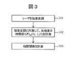
- FIG. 3 is a flowchart showing the flow of processing in the photon detection device 1.
- the semiconductor laser 2 outputs laser light while performing intensity modulation (step 301).
- the upper diagram in FIG. 4 is a diagram in which the horizontal axis represents time T and the vertical axis represents laser intensity, and is a diagram for explaining intensity modulation in the semiconductor laser 2.
- the semiconductor laser 2 outputs a laser while performing intensity modulation between a first intensity (High) and a second intensity (Low) in accordance with an external modulation signal from the external modulator 3.
- the lower diagram in FIG. 4 is a diagram in which the horizontal axis represents time T and the vertical axis represents light intensity I (T), and is a diagram for explaining measurement of signal light intensity temporal fluctuation.
- the solid line in the lower diagram of FIG. 4 indicates the pulse signal output from SPAD5.
- the portion surrounded by the dotted line 401 corresponds to the light intensity when the output of the semiconductor laser 2 is the first intensity (High), and the portion surrounded by the dotted line 402 is the output of the semiconductor laser 2. This corresponds to the light intensity at the second intensity (Low).
- the time fluctuation of the light intensity when the output of the semiconductor laser 2 is the first intensity (High) is defined as I H (T), and the output when the output of the semiconductor laser 2 is the second intensity (Low).
- the time fluctuation of the light intensity is defined as I L (T).
- first intensity is larger than the second intensity
- second strength these simply indicate that the strengths are different, and the magnitudes of the strengths may be reversed.
- the signal distributor 6 receives an external modulation signal from the external modulator 3 and a pulse signal from the SPAD 5.
- the signal distributor 6 synchronizes with the external modulation signal from the external modulator 3 and transmits the time fluctuation I H (T) of the light intensity corresponding to the first intensity (High) to the channel (ch 1) of the correlator 7.
- the time fluctuation I L (T) of the light intensity corresponding to the second intensity (Low) is output to the channel (ch 2) of the correlator 7.
- the correlator 7 calculates a correlation function G ( ⁇ T) between the fluorescence signal intensity I (T) at a certain time T and the fluorescence intensity I (T + ⁇ T) at the time when ⁇ T has elapsed therefrom (step 303).
- the correlator 7 includes ⁇ I H (T) I H (T + ⁇ T)>, ⁇ I H (T) I L (T + ⁇ T)>, ⁇ I L (T) I H (T + ⁇ T)>, ⁇ I L (T)
- the correlation function G ( ⁇ T) is calculated by obtaining I L (T + ⁇ T)>, ⁇ I H (T)>, ⁇ I L (T)>.
- ⁇ . . . > Represents a time average as described above.
- the correlator 7 calculates the correlation function G ( ⁇ T) according to the following equation (2).
- the first term is a term corresponding to a normal correlation signal
- the second term is a contribution term of the after pulse. Therefore, according to the present embodiment, the magnitude of the influence of the after pulse is obtained by evaluating the magnitude of the temporal asymmetry of the pseudo signal of the after pulse, and the magnitude of the influence of the after pulse is subtracted from the normal correlation signal. Thus, accurate correlation measurement can be performed.
- FIG. 5 shows a first example of a signal distributor.
- the signal distributor 6 is configured by a logic operation circuit, and includes a first AND circuit 61, a second AND circuit 62, and a NOT circuit 63.
- the output of the SPAD 5 is input to one input terminal of the first AND circuit 61, and the external modulation signal from the external modulator 3 is input to the other input terminal of the first AND circuit 61. Therefore, the output of the first AND circuit 61 corresponds to the temporal fluctuation I H (T) of the light intensity at the first intensity (High).
- the output of SPAD5 is input to one input terminal of the second AND circuit 62, the external modulation signal from the external modulator 3 is input to the input terminal of the NOT circuit 63, and the output of the NOT circuit 63 is This is input to the other input terminal of the second AND circuit 62. Therefore, the output of the second AND circuit 62 corresponds to the time fluctuation I L (T) of the light intensity at the second intensity (Low).
- the calculation function of the correlation function in the correlator 7 is the same as the expression (2).
- FIG. 6 shows a second example of the signal distributor 6.
- the signal distributor 6 includes an AND circuit 64.
- the output of SPAD5 is directly input to the channel (ch1) of the correlator 7. Therefore, the time fluctuation I H + L (T) of the light intensity in both the first intensity (High) and the second intensity (Low) is input to the channel ch1.
- the output of SPAD 5 is input to one input terminal of AND circuit 64, and the external modulation signal from external modulator 3 is input to the other input terminal of AND circuit 64. Accordingly, the output of the AND circuit 64 corresponds to the temporal fluctuation I H (T) of the light intensity at the first intensity (High). According to the configuration of FIG. 6, the signal distributor 6 can be configured with a simpler circuit.
- the calculation function of the correlation function in the correlator 7 is as shown in the following expression (3).
- I 1 (T) represents the light intensity input to the channel (ch1) of the correlator 7
- I 2 (T) represents the light intensity input to the channel (ch2) of the correlator 7. .
- FIG. 7 shows a third example of the signal distributor 6.
- the signal distributor 6 includes a NOT circuit 65 and an AND circuit 66.
- the output of SPAD5 is directly input to the channel (ch1) of the correlator 7. Therefore, the time fluctuation I H + L (T) of the light intensity in both the first intensity (High) and the second intensity (Low) is input to the channel ch1.
- the output of SPAD 5 is input to one input terminal of AND circuit 66, the external modulation signal from external modulator 3 is input to the input terminal of NOT circuit 65, and the output of NOT circuit 65 is the AND circuit 66. To the other input terminal. Accordingly, the output of the AND circuit 66 corresponds to the light intensity temporal fluctuation I L (T) at the second intensity (Low).
- the calculation function of the correlation function in the correlator 7 is the same as the expression (3).
- the configuration of the signal distributor 6 is not limited thereto. It suffices if the signal distributor 6 can distribute the pulse signal from the SPAD 5 to each channel of the correlator 7 in synchronization with the external modulation signal, and other configurations may be used as long as the pulse signal distribution function can be realized. Further, the calculation formula of the correlation function is not limited to that described above, and may be changed as appropriate.
- OBIS 488 LX manufactured by Coherent was used as the semiconductor laser 2.
- a single photon detector (id100-20) manufactured by IDQ (ID Quantique) was used as SPAD5.
- a signal for laser modulation (corresponding to the external modulator 3) and a signal from a single photon detector were recorded by PCI-6602 manufactured by National Instruments.
- the functions of the signal distributor 6 and the correlator 7 were implemented by a PC (Personal Computer) connected to the PCI-6602, and the distribution of the signals recorded in the PCI-6602 and the calculation of the correlation function were performed.
- the calculation in the correlator 7 was performed according to the above-described equation (2).
- FIG. 8 shows the result of observing scattered light from the surface of the aluminum foil using an aluminum foil as a reference sample.
- the laser intensity was reduced until the peak power reached 5 ⁇ W
- the graph of FIG. 8 shows an average of results obtained by repeating the measurement for about 10 seconds 10 times.
- Correlation 1
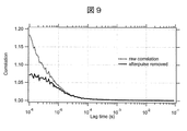
- FIG. 9 shows the result of measuring the scattered light from an aqueous solution of BSA using a 0.4 mg / mL aqueous solution of BSA (bovine serum albumin) as sample 9.
- BSA bovine serum albumin
- the peak power of the laser intensity is 25 mW
- the graph of FIG. 9 shows the average of the results of repeating the measurement for about 12 seconds 9 times.
- the originally expected correlation signal was observed after applying afterpulse removal. From the experimental results, it was confirmed that the influence of the false signal due to the after-pulse phenomenon can be removed using only one detector.
- Non-patent Document 1 the configuration uses two detectors (Non-patent Document 1), there is a problem that the cost is increased and the optical system is complicated. Further, conventionally, there is a problem that the use efficiency of the information of the photon pair detected by the detector is low (50%). On the other hand, in the present embodiment, the influence of the false signal due to the after-pulse phenomenon can be removed with one detector (SPAD). Moreover, the utilization efficiency of the information of the photon pair detected by the detector is improved, and the problem that the signal-to-noise ratio is reduced can be solved.
- Non-Patent Document 2 since the conventional configuration uses an expensive pulse laser device and a TCSPC device (Non-Patent Document 2), there is a problem that the cost of the entire measuring device increases.
- the photon detection device 1 is composed of an inexpensive CW semiconductor laser and a normal correlator, the influence of the false signal due to the after-pulse phenomenon can be achieved with a low-cost and simple configuration. Can be removed.
- a detector other than SPAD photomultiplier tube (PMT), hybrid detector (HPD)
- PMT photomultiplier tube
- HPD hybrid detector
- PMT has a low probability of afterpulses and HPD can almost ignore afterpulses, but their maximum sensitivity is less than SPAD.
- the influence of the false signal due to the after-pulse phenomenon can be removed, so that SPAD having excellent sensitivity can be used.
- this invention is not limited to the Example mentioned above, Various modifications are included.
- the above-described embodiments have been described in detail for easy understanding of the present invention, and are not necessarily limited to those having all the configurations described.
- the photon detection device of the present invention is applied to the FCS.
- the photon detection device of the present invention may be applied to a fluorescence cross correlation spectroscopy (FCCS) measurement device.
- the photon detection device of the present invention may be applied to a dynamic light scattering (DLS) measurement device.
- the photon detection device of the present invention may be applied to a fluorescence microscope.
- the photon detection device of the present invention may be applied to devices other than those described above.
- the configuration of the optical system 4 may be changed as appropriate according to the device to which it is applied.
- FCCS since each molecule that interacts is labeled with a different fluorescent dye and observed, usually, as many photon detectors as the number of fluorescent dyes are required.
- the photon detection device of the present invention can remove the influence of a false signal due to the after-pulse phenomenon with one photon detector (SPAD).
- PAD photon detector
- the output of the semiconductor laser 2 is modulated in two stages of High and Low, but more stages may be used.
- the signal distributor 6 distributes the pulse signal from the SPAD 5 to a plurality of outputs (three or more outputs) according to the intensity modulation, and the number of channels of the correlator 7 is set in accordance with the number of distribution of the signal distributor 6. Increase it.
- the function of the signal distributor described above can be combined with the correlator. In this case, it is possible to omit the signal distributor 6 shown in FIG.
- Photon detector 2 Semiconductor laser (laser light source) 3 External modulator 4 Optical system 6 Signal distributor 7 Correlator 8 Sample stage 9 Sample 41 Dichroic mirror 42 Objective lens 43 Pinhole
Landscapes
- Physics & Mathematics (AREA)
- Health & Medical Sciences (AREA)
- General Physics & Mathematics (AREA)
- Analytical Chemistry (AREA)
- Spectroscopy & Molecular Physics (AREA)
- Life Sciences & Earth Sciences (AREA)
- Chemical & Material Sciences (AREA)
- Biochemistry (AREA)
- General Health & Medical Sciences (AREA)
- Immunology (AREA)
- Pathology (AREA)
- Theoretical Computer Science (AREA)
- Mathematical Physics (AREA)
- Engineering & Computer Science (AREA)
- Nuclear Medicine, Radiotherapy & Molecular Imaging (AREA)
- Investigating, Analyzing Materials By Fluorescence Or Luminescence (AREA)
Abstract
光子検出装置は、変調信号に従って強度変調しながらレーザ光を出力する半導体レーザと、アバランシェダイオードを受光素子とする単一光子検出器と、前記レーザ光を試料に照射し、前記試料からの光を前記単一光子検出器に導くように構成された光学系と、前記変調信号に同期して、前記単一光子検出器からのパルス信号を複数の出力に分配する信号分配器と、前記信号分配器からの前記複数の出力に基づいて相関関数を計算する相関器と、を備える。
Description
本発明は、光子検出装置、光子検出方法、蛍光相関分光測定装置、蛍光相互相関分光測定装置、動的光散乱測定装置、及び、蛍光顕微鏡に関する。
光子相関計測法は、試料溶液中の粒子のサイズの測定や分子間相互作用の検出に広く用いられている。例えば、光子相関計測法としては、蛍光相関分光法(Fluorescence correlation spectroscopy:FCS)や動的光散乱法(Dynamic Light Scattering:DLS)などがある。
光子相関計測法においては、試料溶液からの蛍光(FCS)や光散乱(DLS)に由来する光子信号を時系列に計測し、その時間揺らぎに基づいて様々な物理量を求める。光子相関計測法においては、上記の時間揺らぎを定量化するために、時間相関関数を用いる。ある時間間隔ΔTを伴って検出される2つの光子の対を専用ハードウェアあるいは専用ソフトウェアで計数し、平均光強度で規格化することでΔTにおける相関信号を求める(式1)。

H. C. Burstyn and J. V. Sengers, "Time dependence of critical concentration fluctuations in a binary liquid", Phys. Rev. A 27(2), 1071-1085 (1983)
石井邦彦・田原太平、「時間反転対称性を利用した蛍光相関分光における偽信号の除去」、第6回分子科学討論会要旨1P-086、2012年7月17日
J. Enderlein and I. Gregor, "Using fluorescence lifetime for discriminating detector afterpulsing in fluorescence correlation spectroscopy", Rev. Sci. Instrum. 76(3), 033102 (2005)
光子相関計測法では、光子検出器として、単一光子アバランシェダイオード(以下、SPAD)が広く採用されている。SPADは、光子を検知すると、光子1個につき1つの電圧パルスを出力する。しかしながら、SPADは、光子を検知して電圧パルスを出力した後、数マイクロ秒以内に、ある確率で2つ目の電圧パルス(以下、アフターパルス)を出力する。アフターパルスは、数マイクロ秒の時間領域の相関信号に大きな影響を与える。したがって、SPADを用いた光子相関計測においては、SPADのアフターパルス現象による偽の相関信号が問題となる。
従来の光子相関計測において、特にアフターパルスの影響を回避する必要があるときは、検出器を2台用い、それらの信号の相互相関を計算する方法が一般的であった(非特許文献1)。しかしながら、非特許文献1の従来法では、検出器が2台必要であることからコストがかかり、また、光学系が複雑になるという課題があった。さらに、上記のように異なる検出器で検出された光子対のみを使用することから、同じ検出器で検出された光子対の情報(全光子対の50%)を捨てることになり、信号雑音比が低下するという課題がある。
上記のアフターパルスの偽信号の除去に関し、本願の発明者らは、パルスレーザーと時間相関光子係数法(Time Correlated Single Photon Counting:TCSPC)を用いて相関信号の時間反転対称性を解析する方法を報告した(非特許文献2)。しかしながら、非特許文献2の方法では、高価なパルスレーザー装置とTCSPC装置が必要となるため、測定装置全体のコストが増大するという課題があり、通常の光子相関計測への応用は現実的ではなかった。
また、非特許文献3では、パルスレーザーとTCSPCを用いて、アフターパルス信号と蛍光信号の時間挙動の違いからアフターパルスの影響を評価している。非特許文献3の方法も、非特許文献2の方法と同様に、測定装置全体のコストが増大するという課題がある。
本発明は、このような状況に鑑みてなされたものであり、より簡易な構成でアフターパルス現象による偽信号の影響を除去することが可能な技術を提供する。
上記課題を解決するために、例えば請求の範囲に記載の構成を採用する。本願は上記課題を解決する手段を複数含んでいるが、その一例を挙げるならば、変調信号に従って強度変調しながらレーザ光を出力する半導体レーザと、アバランシェダイオードを受光素子とする単一光子検出器と、前記レーザ光を試料に照射し、前記試料からの光を前記単一光子検出器に導くように構成された光学系と、前記変調信号に同期して、前記単一光子検出器からのパルス信号を複数の出力に分配する信号分配器と、前記信号分配器からの前記複数の出力に基づいて相関関数を計算する相関器と、を備える光子検出装置が提供される。
本発明によれば、より簡易な構成でアフターパルス現象による偽信号の影響を除去することができる。本発明に関連する更なる特徴は、本明細書の記述、添付図面から明らかになるものである。また、上記した以外の、課題、構成および効果は、以下の実施例の説明により明らかにされる。
以下、添付図面を参照して本発明の実施例について説明する。なお、添付図面は本発明の原理に則った具体的な実施例を示しているが、これらは本発明の理解のためのものであり、決して本発明を限定的に解釈するために用いられるものではない。
図1は、本発明の光子検出装置の一実施例の構成図である。図1は、本発明の光子検出装置を蛍光相関分光(FCS)測定装置に適用した例を示す。光子検出装置1は、半導体レーザ(レーザ光源)2と、外部変調器3と、光学系4と、SPAD5と、信号分配器6と、相関器7とを備える。
半導体レーザ2は、連続的にレーザ光を出すCWレーザ(Continuous wave laser)である。外部変調器3は、外部変調信号を半導体レーザ2及び信号分配器6へ出力する。外部変調器3は、半導体レーザ2のレーザ光を強度変調するために使用されており、例えば、数十MHz程度の周波数で変調が可能なものであればよい。半導体レーザ2は、外部変調器3からの外部変調信号に従って強度変調しながらレーザ光を出力する。
光学系4は、半導体レーザ2からのレーザ光を試料台8に載置された試料9に照射し、試料9からの光をSPAD5に導くように構成されている。光学系4は、ダイクロイックミラー41と、対物レンズ42と、ピンホール43とを備える。なお、図1の光学系4に関しては主要な構成要素のみを示しており、これ以外に他の構成要素(ミラー、レンズなど)を含んでもよい。
ダイクロイックミラー41は、半導体レーザ2からのレーザ光(励起光)を反射して、試料9からの蛍光(例えば、励起光で励起される蛍光色素からの蛍光)を透過する光学特性を有する。半導体レーザ2から出たレーザ光は、ダイクロイックミラー41で反射し、その後、対物レンズ42に入射する。対物レンズ42の焦点位置には、試料9が配置されている。試料9から発した蛍光は、再び対物レンズ42を介してダイクロイックミラー41に達する。当該蛍光は、ダイクロイックミラー41を通過し、ピンホール43を経たのち、SPAD5に導かれる。
SPAD5は、アバランシェダイオードを受光素子とする単一光子検出器である。SPAD5は、上述の通り、光子を検知すると光子1個につき1つの電圧パルスを出力する。SPAD5は、ピンホール43を経て受光した光に応じて、パルス信号を信号分配器6に出力する。
信号分配器6は、SPAD5からのパルス信号を2つの出力に分配する。より具体的には、信号分配器6は、外部変調器3からの外部変調信号に同期して、SPAD5からのパルス信号を2つの出力に分配し、それら2つの出力を相関器7の2つのチャネル(ch1、ch2)の各々に入力する。
相関器7は、2つのチャネル(ch1、ch2)に入力された信号に基づいて相関関数を計算する。相関器7における処理は、例えば集積回路で設計する等によりハードウェアで実現されてもよい。また、別の例として、相関器7における処理は、プロセッサがその処理に対応するプログラムを解釈し、実行することによりソフトウェアで実現されてもよい。
次に、アフターパルス現象による偽信号を除去する原理について説明する。図2Aは、レーザ光による励起と、それによって得られる信号光子列を示す。光強度の変化(時間揺らぎ)を、時刻(マクロタイム、T)と励起後からの遅延時間(マイクロタイム、t)の関数I(T;t)として表す。ある時刻Tの蛍光信号強度I(T)とそこからΔT経過した時点でのtに依存する蛍光強度I(T+ΔT;t)の間の相関関数を考える。
ここで、アフターパルスの影響を含まない真の蛍光相関信号と、アフターパルスの由来の相関信号の時間反転対称性について説明する。図2Bは、これらの時間反転対称性を簡単に説明する図である。本願発明者らが非特許文献2で報告している通り、アフターパルスの影響を含まない真の蛍光相関関数は、系が平衡状態にある場合、時間反転ΔT→-ΔTに対して対称になる。一方、アフターパルスの由来の相関関数は、時間反転ΔT→-ΔTに対して非対称なt依存性を示す。
本発明は、上述の時間対称性を利用して相関信号に対するアフターパルス現象の影響の大きさを判定するものである。これにより、アフターパルス現象による偽信号を除去した正確な相関計測を行うことが可能になる。
次に、図1の光子検出装置1の処理の流れについて説明する。図3は、光子検出装置1での処理の流れを示すフローチャートである。
半導体レーザ2は、強度変調しながらレーザ光を出力する(ステップ301)。図4の上側の図は、横軸を時間T、縦軸をレーザの強度とした図であり、半導体レーザ2における強度変調を説明する図である。半導体レーザ2は、外部変調器3からの外部変調信号に従って、第1の強度(High)と第2の強度(Low)との間で強度変調をしながらレーザを出力する。
次に、SPAD5及び信号分配器6を用いて、強度変調に同期して、光強度の時間揺らぎIH(T)、IL(T)を別々に計測する(ステップ302)。図4の下側の図は、横軸を時間T、縦軸を光強度I(T)とした図であり、信号光強度の時間揺らぎの計測を説明する図である。図4の下側の図の実線は、SPAD5から出力されるパルス信号を示す。符号401の点線で囲まれた部分は、半導体レーザ2の出力が第1の強度(High)のときの光強度に対応し、符号402の点線で囲まれた部分は、半導体レーザ2の出力が第2の強度(Low)のときの光強度に対応する。ここでは、半導体レーザ2の出力が第1の強度(High)のときの光強度の時間揺らぎをIH(T)と定義し、半導体レーザ2の出力が第2の強度(Low)のときの光強度の時間揺らぎをIL(T)と定義する。なお、ここでは、第1の強度が第2の強度より大きい例を示すが、これに限定されない。本発明において「第1の強度」、「第2の強度」と表現する場合、これらは単に強度が異なることを表しており、強度の大小が逆であってもよい。
信号分配器6には、外部変調器3からの外部変調信号と、SPAD5からのパルス信号が入力される。信号分配器6は、外部変調器3からの外部変調信号に同期して、第1の強度(High)に対応する光強度の時間揺らぎIH(T)を相関器7のチャネル(ch1)に出力し、第2の強度(Low)に対応する光強度の時間揺らぎIL(T)を相関器7のチャネル(ch2)に出力する。
相関器7は、ある時刻Tの蛍光信号強度I(T)とそこからΔT経過した時点での蛍光強度I(T+ΔT)の間の相関関数G(ΔT)を計算する(ステップ303)。相関器7は、<IH(T)IH(T+ΔT)>、<IH(T)IL(T+ΔT)>、<IL(T)IH(T+ΔT)>、<IL(T)IL(T+ΔT)>、<IH(T)>、<IL(T)>を求めることによって、相関関数G(ΔT)を計算する。ここで、<...>は、上述の通り、時間平均を表す。
より詳細には、相関器7は、以下の式(2)に従って、相関関数G(ΔT)を計算する。

式(2)の右辺において、第1項は通常の相関信号に対応する項であり、第2項はアフターパルスの寄与項である。したがって、本実施例によれば、アフターパルスの偽信号の時間非対称性の大きさを評価することでアフターパルスの影響の大きさを求め、通常の相関信号からアフターパルスの影響の大きさを差し引くことで、正確な相関計測を行うことができる。
次に、信号分配器6の構成について説明する。図5は、信号分配器の第1の例を示す。信号分配器6は、論理演算回路によって構成されており、第1のAND回路61と、第2のAND回路62と、NOT回路63とを備える。
SPAD5の出力が、第1のAND回路61の一方の入力端子に入力され、外部変調器3からの外部変調信号が、第1のAND回路61の他方の入力端子に入力される。したがって、第1のAND回路61の出力は、第1の強度(High)のときの光強度の時間揺らぎIH(T)に対応する。
また、SPAD5の出力が、第2のAND回路62の一方の入力端子に入力され、外部変調器3からの外部変調信号が、NOT回路63の入力端子に入力され、NOT回路63の出力が、第2のAND回路62の他方の入力端子に入力される。したがって、第2のAND回路62の出力は、第2の強度(Low)のときの光強度の時間揺らぎIL(T)に対応する。図5の構成の場合、相関器7における相関関数の計算式は、式(2)と同様である。
図6は、信号分配器6の第2の例を示す。信号分配器6は、AND回路64を備える。SPAD5の出力が、相関器7のチャネル(ch1)に直接入力される。したがって、チャネルch1には、第1の強度(High)と第2の強度(Low)の両方の場合の光強度の時間揺らぎIH+L(T)が入力されることになる。
また、SPAD5の出力が、AND回路64の一方の入力端子に入力され、外部変調器3からの外部変調信号が、AND回路64の他方の入力端子に入力される。したがって、AND回路64の出力は、第1の強度(High)のときの光強度の時間揺らぎIH(T)に対応する。図6の構成によれば、信号分配器6を、より簡易な回路で構成することができる。
図6の構成の場合、相関器7における相関関数の計算式は、以下の式(3)のようになる。
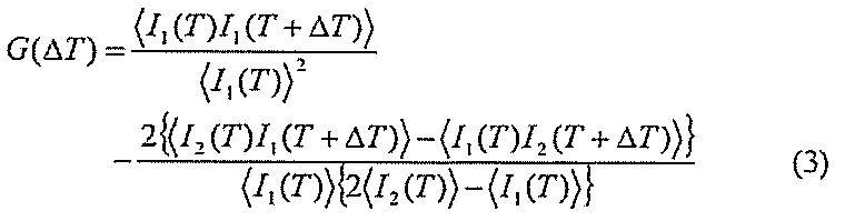
ここで、I1(T)は、相関器7のチャネル(ch1)に入力された光強度を表し、I2(T)は、相関器7のチャネル(ch2)に入力された光強度を表す。
図7は、信号分配器6の第3の例を示す。信号分配器6は、NOT回路65と、AND回路66とを備える。SPAD5の出力が、相関器7のチャネル(ch1)に直接入力される。したがって、チャネルch1には、第1の強度(High)と第2の強度(Low)の両方の場合の光強度の時間揺らぎIH+L(T)が入力されることになる。
また、SPAD5の出力が、AND回路66の一方の入力端子に入力され、外部変調器3からの外部変調信号が、NOT回路65の入力端子に入力され、NOT回路65の出力が、AND回路66の他方の入力端子に入力される。したがって、AND回路66の出力は、第2の強度(Low)のときの光強度の時間揺らぎIL(T)に対応する。図7の構成の場合、相関器7における相関関数の計算式は、式(3)と同様である。
上述では、信号分配器6の3つの例を説明したが、信号分配器6の構成はこれらに限定されない。信号分配器6が外部変調信号に同期してSPAD5からのパルス信号を相関器7の各チャネルに分配できればよく、パルス信号の分配機能が実現できるならば他の構成でもかまわない。また、相関関数の計算式も上述したものに限定されず、適宜変更されてよい。
図8及び図9は、実験結果を示すグラフである。当該実験において、半導体レーザ2としてCoherent社製のOBIS 488 LXを使用した。また、SPAD5としてIDQ(ID Quantique)社製のシングルフォトンディテクタ(id100-20)を使用した。また、National Instruments社製のPCI-6602によって、レーザ変調のための信号の出力(外部変調器3に相当)、及び、シングルフォトンディテクタからの信号の記録を行った。PCI-6602に接続したPC(Personal Computer)によって信号分配器6及び相関器7の機能を実装し、PCI-6602に記録された信号の分配及び相関関数の計算を行った。なお、相関器7での計算は、上述の式(2)に従って行った。
図8は、参照試料としてアルミホイルを使用し、アルミホイルの表面からの散乱光を観測した結果を示す。なお、当該実験において、レーザ強度はピークパワーで5μWになるまで減光し、図8のグラフは、約10秒の測定を10回繰り返した結果の平均を示す。参照試料での実験に関して、アフターパルスの影響がない場合、相関がない(Correlation = 1)ことが期待されるが、ほぼ期待通りの結果となった。
図9は、試料9としてBSA(ウシ血清アルブミン)の0.4mg/mL水溶液を使用し、BSAの水溶液からの散乱光を測定した結果を示す。当該実験において、レーザ強度のピークパワーは25mWであり、図9のグラフは、約12秒の測定を9回繰り返した結果の平均を示す。図9に示すように、アフターパルス除去を適用した後に本来期待される相関信号が観測できた。当該実験結果から、1台の検出器のみを用いてアフターパルス現象による偽信号の影響を除去できることが確認できた。
上述した実施例の効果について説明する。従来では、2台の検出器を用いる構成(非特許文献1)であったため、コストがかかり、光学系が複雑になるという課題があった。また、従来では、検出器で検出された光子対の情報の利用効率が低い(50%)という課題もあった。これに対して、本実施例では、1台の検出器(SPAD)でアフターパルス現象による偽信号の影響を除去することができる。また、検出器で検出された光子対の情報の利用効率も向上し、信号雑音比が低下するという課題を解決することができる。
また、従来では、高価なパルスレーザー装置とTCSPC装置を用いる構成(非特許文献2)であったため、測定装置全体のコストが増大するという課題があった。これに対して、上述の実施例によれば、光子検出装置1が安価なCW半導体レーザと通常の相関器から構成されるので、低コストかつ簡易な構成によって、アフターパルス現象による偽信号の影響を除去することができる。
また、光子相関計測では、SPAD以外の検出器(光電子増倍管(PMT)、ハイブリッド検出器(HPD))を使う場合もあり得る。PMTはアフターパルスの確率が低く、また、HPDはアフターパルスをほぼ無視できるが、これらの最高感度はSPADに及ばない。本実施例では、アフターパルス現象による偽信号の影響を除去することができるため、感度に優れたSPADを利用することが可能となる。
なお、本発明は上述した実施例に限定されるものではなく、様々な変形例が含まれる。例えば、上述した実施例は本発明を分かりやすく説明するために詳細に説明したものであり、必ずしも説明した全ての構成を備えるものに限定されるものではない。また、実施例の構成の一部について、他の構成の追加・削除・置換をすることが可能である。
上述では、本発明の光子検出装置をFCSに適用した例を示したが、本発明の光子検出装置は、蛍光相互相関分光(FCCS)測定装置に適用されてもよい。また、本発明の光子検出装置は、動的光散乱(DLS)測定装置に適用されてもよい。また、本発明の光子検出装置は、蛍光顕微鏡に適用されてもよい。さらに、本発明の光子検出装置は、上記以外の他の装置に適用されてもよい。なお、光学系4の構成は、適用する装置に応じて適宜変更されてよい。
なお、本発明をFCCSに適用した場合、以下の利点がある。FCCSでは、相互作用する分子ごとに異なる蛍光色素で標識して観察するため、通常、蛍光色素の数だけ光子検出装置を要する。上述のように、本発明の光子検出装置は、1台の光子検出器(SPAD)でアフターパルス現象による偽信号の影響を除去できることから、FCCSにおいては、非特許文献1の従来法に対して、本発明の光子検出装置を備えていることの優位性は一層大きい。
上述では、半導体レーザ2の出力をHighとLowの2段に変調したが、これより多い多段変調にしてもよい。この場合、信号分配器6が強度変調に従ってSPAD5からのパルス信号を複数の出力(3つ以上の出力)に分配し、かつ、信号分配器6の分配数に合わせて相関器7のチャネル数を増やせばよい。
例えば、入力部分にゲートを備えた相関器が提供されるならば、上述した信号分配器の機能を相関器で兼ねることも可能である。この場合、図1等に記載した信号分配器6を省略することも可能である。
1 光子検出装置
2 半導体レーザ(レーザ光源)
3 外部変調器
4 光学系
6 信号分配器
7 相関器
8 試料台
9 試料
41 ダイクロイックミラー
42 対物レンズ
43 ピンホール
2 半導体レーザ(レーザ光源)
3 外部変調器
4 光学系
6 信号分配器
7 相関器
8 試料台
9 試料
41 ダイクロイックミラー
42 対物レンズ
43 ピンホール
Claims (8)
- 変調信号に従って強度変調しながらレーザ光を出力する半導体レーザと、
アバランシェダイオードを受光素子とする単一光子検出器と、
前記レーザ光を試料に照射し、前記試料からの光を前記単一光子検出器に導くように構成された光学系と、
前記変調信号に同期して、前記単一光子検出器からのパルス信号を複数の出力に分配する信号分配器と、
前記信号分配器からの前記複数の出力に基づいて相関関数を計算する相関器と、
を備える光子検出装置。 - 請求項1に記載の光子検出装置において、
前記半導体レーザは、第1の強度と第2の強度との間で強度変調をしながら前記レーザ光を出力し、
前記信号分配器は、前記単一光子検出器からのパルス信号を、前記第1の強度のときのパルス信号である第1の出力と、前記第2の強度のときのパルス信号である第2の出力とに分配することを特徴とする光子検出装置。 - 請求項1に記載の光子検出装置において、
前記半導体レーザは、第1の強度と第2の強度との間で強度変調をしながら前記レーザ光を出力し、
前記信号分配器は、前記単一光子検出器からのパルス信号を、前記第1の強度及び前記第2の強度のときのパルス信号である第1の出力と、前記第1の強度のときのパルス信号である第2の出力とに分配することを特徴とする光子検出装置。 - 請求項1から3のいずれか一項に記載の光子検出装置を備える蛍光相関分光測定装置。
- 請求項1から3のいずれか一項に記載の光子検出装置を備える蛍光相互相関分光測定装置。
- 請求項1から3のいずれか一項に記載の光子検出装置を備える動的光散乱測定装置。
- 請求項1から3のいずれか一項に記載の光子検出装置を備える蛍光顕微鏡。
- 半導体レーザにより、変調信号に従って強度変調しながらレーザ光を出力するステップと、
光学系により、前記レーザ光を試料に照射し、前記試料からの光を、アバランシェダイオードを受光素子とする単一光子検出器に導くステップと、
前記単一光子検出器により、前記試料からの光を検出するステップと、
信号分配器により、前記変調信号に同期して、前記単一光子検出器からのパルス信号を複数の出力に分配するステップと、
相関器により、前記信号分配器からの前記複数の出力に基づいて相関関数を計算するステップと、
を含む光子検出方法。
Applications Claiming Priority (2)
| Application Number | Priority Date | Filing Date | Title |
|---|---|---|---|
| JP2015-219557 | 2015-11-09 | ||
| JP2015219557 | 2015-11-09 |
Publications (1)
| Publication Number | Publication Date |
|---|---|
| WO2017082218A1 true WO2017082218A1 (ja) | 2017-05-18 |
Family
ID=58695269
Family Applications (1)
| Application Number | Title | Priority Date | Filing Date |
|---|---|---|---|
| PCT/JP2016/083010 Ceased WO2017082218A1 (ja) | 2015-11-09 | 2016-11-08 | 光子検出装置、光子検出方法、蛍光相関分光測定装置、蛍光相互相関分光測定装置、動的光散乱測定装置、及び、蛍光顕微鏡 |
Country Status (1)
| Country | Link |
|---|---|
| WO (1) | WO2017082218A1 (ja) |
Cited By (5)
| Publication number | Priority date | Publication date | Assignee | Title |
|---|---|---|---|---|
| WO2019058438A1 (ja) * | 2017-09-20 | 2019-03-28 | オリンパス株式会社 | 光計測装置、光計測方法および走査型顕微鏡 |
| CN111868556A (zh) * | 2018-02-13 | 2020-10-30 | 感应光子公司 | 用于高分辨率远程闪速lidar的方法和系统 |
| JP2022077588A (ja) * | 2020-11-12 | 2022-05-24 | 国立研究開発法人物質・材料研究機構 | 動的光散乱測定装置、動的光散乱測定・解析方法、および、測定・解析プログラム |
| US11978754B2 (en) | 2018-02-13 | 2024-05-07 | Sense Photonics, Inc. | High quantum efficiency Geiger-mode avalanche diodes including high sensitivity photon mixing structures and arrays thereof |
| WO2024235929A1 (en) | 2023-05-17 | 2024-11-21 | Universite De Geneve | Particle characterization system |
Citations (4)
| Publication number | Priority date | Publication date | Assignee | Title |
|---|---|---|---|---|
| JP2007530916A (ja) * | 2003-07-17 | 2007-11-01 | アイシス イノベイシヨン リミテツド | 蛍光寿命の測定装置及び方法 |
| WO2012111093A1 (ja) * | 2011-02-15 | 2012-08-23 | 有限会社ワイ・システムズ | キャリア寿命の測定方法および測定装置 |
| JP2013520646A (ja) * | 2010-02-19 | 2013-06-06 | ライトシップ メディカル リミテッド | 蛍光測定 |
| JP2015087171A (ja) * | 2013-10-29 | 2015-05-07 | 浜松ホトニクス株式会社 | 蛍光イメージング装置 |
-
2016
- 2016-11-08 WO PCT/JP2016/083010 patent/WO2017082218A1/ja not_active Ceased
Patent Citations (4)
| Publication number | Priority date | Publication date | Assignee | Title |
|---|---|---|---|---|
| JP2007530916A (ja) * | 2003-07-17 | 2007-11-01 | アイシス イノベイシヨン リミテツド | 蛍光寿命の測定装置及び方法 |
| JP2013520646A (ja) * | 2010-02-19 | 2013-06-06 | ライトシップ メディカル リミテッド | 蛍光測定 |
| WO2012111093A1 (ja) * | 2011-02-15 | 2012-08-23 | 有限会社ワイ・システムズ | キャリア寿命の測定方法および測定装置 |
| JP2015087171A (ja) * | 2013-10-29 | 2015-05-07 | 浜松ホトニクス株式会社 | 蛍光イメージング装置 |
Non-Patent Citations (2)
| Title |
|---|
| BOIKO, D. L. ET AL.: "On the application of a monolithic array for detecting intensity- correlated photons emitted by different source types", OPTICS EXPRESS, vol. 17, no. 17, 17 August 2009 (2009-08-17), pages 15087 - 15103, XP055382046 * |
| ZHAO, M. ET AL.: "Afterpulsing and its correction in fluorescence correlation spectroscopy experiments", APPLIED OPTICS, vol. 42, no. 19, 1 July 2003 (2003-07-01), pages 4031 - 4036, XP055382047 * |
Cited By (8)
| Publication number | Priority date | Publication date | Assignee | Title |
|---|---|---|---|---|
| WO2019058438A1 (ja) * | 2017-09-20 | 2019-03-28 | オリンパス株式会社 | 光計測装置、光計測方法および走査型顕微鏡 |
| WO2019058619A1 (ja) * | 2017-09-20 | 2019-03-28 | オリンパス株式会社 | 光計測装置、光計測方法および走査型顕微鏡 |
| US11237047B2 (en) | 2017-09-20 | 2022-02-01 | Olympus Corporation | Optical measurement device, optical measurement method, and scanning microscope |
| CN111868556A (zh) * | 2018-02-13 | 2020-10-30 | 感应光子公司 | 用于高分辨率远程闪速lidar的方法和系统 |
| US11978754B2 (en) | 2018-02-13 | 2024-05-07 | Sense Photonics, Inc. | High quantum efficiency Geiger-mode avalanche diodes including high sensitivity photon mixing structures and arrays thereof |
| JP2022077588A (ja) * | 2020-11-12 | 2022-05-24 | 国立研究開発法人物質・材料研究機構 | 動的光散乱測定装置、動的光散乱測定・解析方法、および、測定・解析プログラム |
| JP7473200B2 (ja) | 2020-11-12 | 2024-04-23 | 国立研究開発法人物質・材料研究機構 | 動的光散乱測定装置、動的光散乱測定・解析方法、および、測定・解析プログラム |
| WO2024235929A1 (en) | 2023-05-17 | 2024-11-21 | Universite De Geneve | Particle characterization system |
Similar Documents
| Publication | Publication Date | Title |
|---|---|---|
| US20240353309A1 (en) | Multi-Modal Fluorescence Imaging Flow Cytometry System | |
| US20250155353A1 (en) | Fluorescence Imaging Flow Cytometry With Enhanced Image Resolution | |
| WO2017082218A1 (ja) | 光子検出装置、光子検出方法、蛍光相関分光測定装置、蛍光相互相関分光測定装置、動的光散乱測定装置、及び、蛍光顕微鏡 | |
| KR101752588B1 (ko) | 형광 수명 측정 시스템 및 방법 | |
| US10539495B2 (en) | Systems and methods for generating an image of an inspection object using an attenuated beam | |
| JP6703215B1 (ja) | 光学測定装置及び光学測定方法 | |
| JP2022525605A (ja) | 高周波多重励起データを使用した蛍光イメージングのスペクトルアンミックス | |
| JP2011513740A (ja) | 光子混合検出器を用いた時間分解分光分析方法およびシステム | |
| EP3306761A1 (en) | Light source device and inspection device | |
| JP4620786B2 (ja) | 蛍光検出方法、蛍光検出装置及びプログラム | |
| JP2017116423A (ja) | 光ファイバ特性測定装置および光ファイバ特性測定方法 | |
| US8649010B2 (en) | Integral transformed optical measurement method and apparatus | |
| US11280736B2 (en) | Fluorescence lifetime measurement device for analyzing multi-exponential decay function type experimental data at high speed and measurement method therefor | |
| US11327002B2 (en) | In-liquid microparticle analysis system and in-liquid microparticle analysis method | |
| CN111929251A (zh) | 一种基于关联成像的微小目标检测装置及方法 | |
| WO2023109603A1 (zh) | 对样品进行光谱测定的方法、系统以及流式细胞仪 | |
| KR20260046434A (ko) | 광학 측정 장치 및 광학 측정 방법 | |
| JP2015203654A (ja) | 分子数測定装置及び分子数測定方法 | |
| KR20260000184A (ko) | 위상자 역연산을 이용하여 형광 수명을 측정하기 위한 장치 및 방법 | |
| JP2025011743A (ja) | 液体中微粒子分析システム | |
| Charbon | Precision imaging for biosensing | |
| JP2007534955A (ja) | 自己相関関数を決定する方法 |
Legal Events
| Date | Code | Title | Description |
|---|---|---|---|
| 121 | Ep: the epo has been informed by wipo that ep was designated in this application |
Ref document number: 16864179 Country of ref document: EP Kind code of ref document: A1 |
|
| NENP | Non-entry into the national phase |
Ref country code: DE |
|
| 122 | Ep: pct application non-entry in european phase |
Ref document number: 16864179 Country of ref document: EP Kind code of ref document: A1 |
|
| NENP | Non-entry into the national phase |
Ref country code: JP |