WO2017056739A1 - レーザ加工方法 - Google Patents
レーザ加工方法 Download PDFInfo
- Publication number
- WO2017056739A1 WO2017056739A1 PCT/JP2016/073355 JP2016073355W WO2017056739A1 WO 2017056739 A1 WO2017056739 A1 WO 2017056739A1 JP 2016073355 W JP2016073355 W JP 2016073355W WO 2017056739 A1 WO2017056739 A1 WO 2017056739A1
- Authority
- WO
- WIPO (PCT)
- Prior art keywords
- modified region
- silicon substrate
- cutting line
- laser beam
- semiconductor substrate
- Prior art date
- Legal status (The legal status is an assumption and is not a legal conclusion. Google has not performed a legal analysis and makes no representation as to the accuracy of the status listed.)
- Ceased
Links
Images












Classifications
-
- H—ELECTRICITY
- H10—SEMICONDUCTOR DEVICES; ELECTRIC SOLID-STATE DEVICES NOT OTHERWISE PROVIDED FOR
- H10P—GENERIC PROCESSES OR APPARATUS FOR THE MANUFACTURE OR TREATMENT OF DEVICES COVERED BY CLASS H10
- H10P54/00—Cutting or separating of wafers, substrates or parts of devices
-
- B—PERFORMING OPERATIONS; TRANSPORTING
- B23—MACHINE TOOLS; METAL-WORKING NOT OTHERWISE PROVIDED FOR
- B23K—SOLDERING OR UNSOLDERING; WELDING; CLADDING OR PLATING BY SOLDERING OR WELDING; CUTTING BY APPLYING HEAT LOCALLY, e.g. FLAME CUTTING; WORKING BY LASER BEAM
- B23K26/00—Working by laser beam, e.g. welding, cutting or boring
- B23K26/02—Positioning or observing the workpiece, e.g. with respect to the point of impact; Aligning, aiming or focusing the laser beam
- B23K26/04—Automatically aligning, aiming or focusing the laser beam, e.g. using the back-scattered light
- B23K26/046—Automatically focusing the laser beam
-
- B—PERFORMING OPERATIONS; TRANSPORTING
- B23—MACHINE TOOLS; METAL-WORKING NOT OTHERWISE PROVIDED FOR
- B23K—SOLDERING OR UNSOLDERING; WELDING; CLADDING OR PLATING BY SOLDERING OR WELDING; CUTTING BY APPLYING HEAT LOCALLY, e.g. FLAME CUTTING; WORKING BY LASER BEAM
- B23K26/00—Working by laser beam, e.g. welding, cutting or boring
- B23K26/50—Working by transmitting the laser beam through or within the workpiece
- B23K26/53—Working by transmitting the laser beam through or within the workpiece for modifying or reforming the material inside the workpiece, e.g. for producing break initiation cracks
-
- H—ELECTRICITY
- H10—SEMICONDUCTOR DEVICES; ELECTRIC SOLID-STATE DEVICES NOT OTHERWISE PROVIDED FOR
- H10P—GENERIC PROCESSES OR APPARATUS FOR THE MANUFACTURE OR TREATMENT OF DEVICES COVERED BY CLASS H10
- H10P34/00—Irradiation with electromagnetic or particle radiation of wafers, substrates or parts of devices
- H10P34/40—Irradiation with electromagnetic or particle radiation of wafers, substrates or parts of devices with high-energy radiation
- H10P34/42—Irradiation with electromagnetic or particle radiation of wafers, substrates or parts of devices with high-energy radiation with electromagnetic radiation, e.g. laser annealing
-
- H—ELECTRICITY
- H10—SEMICONDUCTOR DEVICES; ELECTRIC SOLID-STATE DEVICES NOT OTHERWISE PROVIDED FOR
- H10P—GENERIC PROCESSES OR APPARATUS FOR THE MANUFACTURE OR TREATMENT OF DEVICES COVERED BY CLASS H10
- H10P52/00—Grinding, lapping or polishing of wafers, substrates or parts of devices
-
- H—ELECTRICITY
- H10—SEMICONDUCTOR DEVICES; ELECTRIC SOLID-STATE DEVICES NOT OTHERWISE PROVIDED FOR
- H10P—GENERIC PROCESSES OR APPARATUS FOR THE MANUFACTURE OR TREATMENT OF DEVICES COVERED BY CLASS H10
- H10P72/00—Handling or holding of wafers, substrates or devices during manufacture or treatment thereof
- H10P72/70—Handling or holding of wafers, substrates or devices during manufacture or treatment thereof for supporting or gripping
- H10P72/74—Handling or holding of wafers, substrates or devices during manufacture or treatment thereof for supporting or gripping using temporarily an auxiliary support
- H10P72/7402—Wafer tapes, e.g. grinding or dicing support tapes
-
- H—ELECTRICITY
- H10—SEMICONDUCTOR DEVICES; ELECTRIC SOLID-STATE DEVICES NOT OTHERWISE PROVIDED FOR
- H10P—GENERIC PROCESSES OR APPARATUS FOR THE MANUFACTURE OR TREATMENT OF DEVICES COVERED BY CLASS H10
- H10P95/00—Generic processes or apparatus for manufacture or treatments not covered by the other groups of this subclass
-
- H—ELECTRICITY
- H10—SEMICONDUCTOR DEVICES; ELECTRIC SOLID-STATE DEVICES NOT OTHERWISE PROVIDED FOR
- H10W—GENERIC PACKAGES, INTERCONNECTIONS, CONNECTORS OR OTHER CONSTRUCTIONAL DETAILS OF DEVICES COVERED BY CLASS H10
- H10W42/00—Arrangements for protection of devices
- H10W42/121—Arrangements for protection of devices protecting against mechanical damage
-
- H—ELECTRICITY
- H10—SEMICONDUCTOR DEVICES; ELECTRIC SOLID-STATE DEVICES NOT OTHERWISE PROVIDED FOR
- H10W—GENERIC PACKAGES, INTERCONNECTIONS, CONNECTORS OR OTHER CONSTRUCTIONAL DETAILS OF DEVICES COVERED BY CLASS H10
- H10W46/00—Marks applied to devices, e.g. for alignment or identification
-
- B—PERFORMING OPERATIONS; TRANSPORTING
- B23—MACHINE TOOLS; METAL-WORKING NOT OTHERWISE PROVIDED FOR
- B23K—SOLDERING OR UNSOLDERING; WELDING; CLADDING OR PLATING BY SOLDERING OR WELDING; CUTTING BY APPLYING HEAT LOCALLY, e.g. FLAME CUTTING; WORKING BY LASER BEAM
- B23K2103/00—Materials to be soldered, welded or cut
- B23K2103/50—Inorganic materials other than metals or composite materials
- B23K2103/56—Inorganic materials other than metals or composite materials being semiconducting
-
- H—ELECTRICITY
- H10—SEMICONDUCTOR DEVICES; ELECTRIC SOLID-STATE DEVICES NOT OTHERWISE PROVIDED FOR
- H10P—GENERIC PROCESSES OR APPARATUS FOR THE MANUFACTURE OR TREATMENT OF DEVICES COVERED BY CLASS H10
- H10P72/00—Handling or holding of wafers, substrates or devices during manufacture or treatment thereof
- H10P72/70—Handling or holding of wafers, substrates or devices during manufacture or treatment thereof for supporting or gripping
- H10P72/74—Handling or holding of wafers, substrates or devices during manufacture or treatment thereof for supporting or gripping using temporarily an auxiliary support
- H10P72/7416—Handling or holding of wafers, substrates or devices during manufacture or treatment thereof for supporting or gripping using temporarily an auxiliary support used during dicing or grinding
- H10P72/742—Handling or holding of wafers, substrates or devices during manufacture or treatment thereof for supporting or gripping using temporarily an auxiliary support used during dicing or grinding involving stretching of the auxiliary support post dicing
-
- H—ELECTRICITY
- H10—SEMICONDUCTOR DEVICES; ELECTRIC SOLID-STATE DEVICES NOT OTHERWISE PROVIDED FOR
- H10P—GENERIC PROCESSES OR APPARATUS FOR THE MANUFACTURE OR TREATMENT OF DEVICES COVERED BY CLASS H10
- H10P72/00—Handling or holding of wafers, substrates or devices during manufacture or treatment thereof
- H10P72/70—Handling or holding of wafers, substrates or devices during manufacture or treatment thereof for supporting or gripping
- H10P72/74—Handling or holding of wafers, substrates or devices during manufacture or treatment thereof for supporting or gripping using temporarily an auxiliary support
- H10P72/744—Details of chemical or physical process used for separating the auxiliary support from a device or a wafer
- H10P72/7442—Separation by peeling
-
- H—ELECTRICITY
- H10—SEMICONDUCTOR DEVICES; ELECTRIC SOLID-STATE DEVICES NOT OTHERWISE PROVIDED FOR
- H10W—GENERIC PACKAGES, INTERCONNECTIONS, CONNECTORS OR OTHER CONSTRUCTIONAL DETAILS OF DEVICES COVERED BY CLASS H10
- H10W46/00—Marks applied to devices, e.g. for alignment or identification
- H10W46/501—Marks applied to devices, e.g. for alignment or identification for use before dicing
- H10W46/503—Located in scribe lines
Definitions
- the semiconductor substrate may be a silicon substrate, and the laser beam may have a wavelength greater than 1064 nm.
- the thickness of the silicon substrate from the first modified region and the second modified region is increased with the formation of the first modified region and the second modified region, as compared with the case where laser light having a wavelength of 1064 nm or less is used.
- the crack can be greatly extended in the direction.
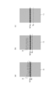
- FIG. 17B is a view showing a photograph of the surface side of the silicon substrate after cutting when the offset amount is 4 ⁇ m.
- FIG. 17C is a view showing a photograph of the surface side of the silicon substrate after cutting when the offset amount is 6 ⁇ m.
- FIG. 18A is a diagram showing a surface perpendicular to the planned cutting line of the silicon substrate when the offset amount is small.
- FIG. 18B is a diagram showing a surface perpendicular to the planned cutting line of the silicon substrate when the offset amount is large.
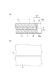
- FIG. 19 is a cross-sectional view for explaining a method of manufacturing a semiconductor chip using the laser processing method of the embodiment.
- FIG. 20 is a cross-sectional view for explaining a semiconductor chip manufacturing method using the laser processing method of the embodiment.
- a plate-like member for example, a substrate, a wafer, or the like
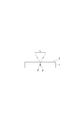
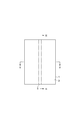
- a scheduled cutting line 5 for cutting the workpiece 1 is set in the workpiece 1.
- the planned cutting line 5 is a virtual line extending linearly.
- the laser beam L is cut in a state where the condensing point (condensing position) P is aligned with the inside of the workpiece 1 as shown in FIG. 3. It moves relatively along the planned line 5 (that is, in the direction of arrow A in FIG. 2).
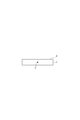
- the modified region 7 is formed on the workpiece 1 along the planned cutting line 5, and the modified region formed along the planned cutting line 5. 7 becomes the cutting start region 8.
- the condensing point P is a portion where the laser light L is condensed.
- the planned cutting line 5 is not limited to a straight line, but may be a curved line, a three-dimensional shape in which these lines are combined, or a coordinate designated.
- the planned cutting line 5 is not limited to a virtual line but may be a line actually drawn on the surface 3 of the workpiece 1.
- the modified region 7 may be formed continuously or intermittently.
- the modified region 7 may be in the form of a line or a dot. In short, the modified region 7 only needs to be formed at least inside the workpiece 1.
- a crack may be formed starting from the modified region 7, and the crack and the modified region 7 may be exposed on the outer surface (front surface 3, back surface, or outer peripheral surface) of the workpiece 1. .
- the laser light incident surface when forming the modified region 7 is not limited to the front surface 3 of the workpiece 1 and may be the back surface of the workpiece 1.
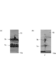
- FIG. 12 is a view showing a photograph of the silicon substrate 10 when the condensing point P of the laser beam L1 is not offset when forming the second modified region 7b.
- FIG. 12A is a diagram showing a photograph of a plane parallel to the planned cutting line of the silicon substrate 10 after the first modified region 7a and the second modified region 7b are formed.
- FIG. 12B is a view showing a photograph of a plane perpendicular to the planned cutting line of the silicon substrate 10 after the first modified region 7a and the second modified region 7b are formed. Referring to (b) of FIG.
- the number of the splashes S generated in the regions separated by 20 ⁇ m or more on both sides from the scheduled cutting line 5 is counted particularly because the characteristics of the functional elements formed on the surface 10 a of the silicon substrate 10 are such splashes S. This is because it causes a problem of deterioration. Dicing streets (regions between adjacent functional elements) are often provided in regions within 20 ⁇ m on both sides of the planned cutting line 5, so that the splash S generated in the region causes a problem of deteriorating the characteristics of the functional devices. Unlikely.
- the movement of the first condensing point P1 and the second condensing point P2 of the laser light L with respect to the scheduled cutting line 5 may be realized by the operation on the condensing lens 105 side, It may be realized by both operations on the optical lens 105 side.
- the first modified region 7a and the second modified region 7b are accompanied by the formation of the first modified region 7a and the second modified region 7b.
- the crack F can be further extended in the thickness direction of the silicon substrate 10.
- the laser beam L1 having a wavelength of 1342 ⁇ m can extend the crack F more greatly.
Landscapes
- Physics & Mathematics (AREA)
- Optics & Photonics (AREA)
- Engineering & Computer Science (AREA)
- Plasma & Fusion (AREA)
- Mechanical Engineering (AREA)
- Chemical & Material Sciences (AREA)
- Chemical Kinetics & Catalysis (AREA)
- General Chemical & Material Sciences (AREA)
- Oil, Petroleum & Natural Gas (AREA)
- Laser Beam Processing (AREA)
- Dicing (AREA)
- Electromagnetism (AREA)
Abstract
Description
Claims (7)
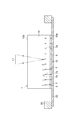
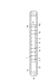
- 表面に複数の機能素子が形成された半導体基板を含む加工対象物に、前記半導体基板の裏面をレーザ光入射面としてレーザ光を集光させて、前記半導体基板の前記表面と前記レーザ光の第1集光点との距離を第1距離に維持しつつ、隣り合う前記機能素子の間を通るように設定された切断予定ラインに沿って前記レーザ光の前記第1集光点を移動させることで、前記切断予定ラインに沿って第1改質領域を形成する第1工程と、
前記第1工程の後に、前記加工対象物に、前記半導体基板の前記裏面をレーザ光入射面として前記レーザ光を集光させて、前記半導体基板の前記表面と前記レーザ光の第2集光点との距離を前記第1距離よりも大きい第2距離に維持しつつ、且つ、前記レーザ光の前記第1集光点を合わせた位置に対して、前記半導体基板の厚さ方向及び前記切断予定ラインの延在方向の両方向に垂直な方向に前記レーザ光の前記第2集光点をオフセットさせつつ、前記切断予定ラインに沿って前記レーザ光の前記第2集光点を移動させることで、前記切断予定ラインに沿って第2改質領域を形成する第2工程と、
前記第2工程の後に、前記半導体基板において前記裏面及び少なくとも前記第2改質領域を含む所定部分を除去する第3工程と、を備える、レーザ加工方法。 - 前記第3工程では、前記半導体基板において前記第1改質領域をさらに含む前記所定部分を除去する、請求項1に記載のレーザ加工方法。
- 前記半導体基板は、シリコン基板であり、
前記レーザ光は、1064nmよりも大きい波長を有する、請求項1又は2に記載のレーザ加工方法。 - 前記レーザ光は、1099μm以上1342μm以下の波長を有する、請求項3に記載のレーザ加工方法。
- 前記レーザ光の前記第1集光点を合わせた位置に対して、前記シリコン基板の前記厚さ方向及び前記切断予定ラインの前記延在方向の両方向に垂直な前記方向に前記レーザ光の前記第2集光点をオフセットさせる距離は、24μm以下である、請求項3又は4に記載のレーザ加工方法。
- 前記レーザ光の前記第1集光点を合わせた位置に対して、前記シリコン基板の前記厚さ方向及び前記切断予定ラインの前記延在方向の両方向に垂直な前記方向に前記レーザ光の前記第2集光点をオフセットさせる前記距離は、4μm以上18μm以下である、請求項5に記載のレーザ加工方法。
- 前記第2工程では、前記第2改質領域を形成することにより、前記第1改質領域及び前記第2改質領域から前記半導体基板の厚さ方向に伸展した亀裂を前記半導体基板の表面に到達させ、
前記第3工程では、前記所定部分を除去することにより、前記所定部分が除去された前記半導体基板の前記裏面に、前記第2工程において前記第1改質領域及び前記第2改質領域から前記半導体基板の厚さ方向に伸展した亀裂を到達させる、請求項1~6の何れか一項に記載のレーザ加工方法。
Priority Applications (5)
| Application Number | Priority Date | Filing Date | Title |
|---|---|---|---|
| US15/763,605 US10290545B2 (en) | 2015-09-29 | 2016-08-08 | Laser processing method |
| CN201680056475.XA CN108028189B (zh) | 2015-09-29 | 2016-08-08 | 激光加工方法 |
| DE112016004419.4T DE112016004419B4 (de) | 2015-09-29 | 2016-08-08 | Laserbearbeitungsverfahren |
| KR1020187011383A KR102566316B1 (ko) | 2015-09-29 | 2016-08-08 | 레이저 가공 방법 |
| US16/388,209 US10755980B2 (en) | 2015-09-29 | 2019-04-18 | Laser processing method |
Applications Claiming Priority (2)
| Application Number | Priority Date | Filing Date | Title |
|---|---|---|---|
| JP2015-191095 | 2015-09-29 | ||
| JP2015191095A JP6605278B2 (ja) | 2015-09-29 | 2015-09-29 | レーザ加工方法 |
Related Child Applications (2)
| Application Number | Title | Priority Date | Filing Date |
|---|---|---|---|
| US15/763,605 A-371-Of-International US10290545B2 (en) | 2015-09-29 | 2016-08-08 | Laser processing method |
| US16/388,209 Continuation US10755980B2 (en) | 2015-09-29 | 2019-04-18 | Laser processing method |
Publications (1)
| Publication Number | Publication Date |
|---|---|
| WO2017056739A1 true WO2017056739A1 (ja) | 2017-04-06 |
Family
ID=58423492
Family Applications (1)
| Application Number | Title | Priority Date | Filing Date |
|---|---|---|---|
| PCT/JP2016/073355 Ceased WO2017056739A1 (ja) | 2015-09-29 | 2016-08-08 | レーザ加工方法 |
Country Status (7)
| Country | Link |
|---|---|
| US (2) | US10290545B2 (ja) |
| JP (1) | JP6605278B2 (ja) |
| KR (1) | KR102566316B1 (ja) |
| CN (1) | CN108028189B (ja) |
| DE (1) | DE112016004419B4 (ja) |
| TW (1) | TWI721006B (ja) |
| WO (1) | WO2017056739A1 (ja) |
Families Citing this family (11)
| Publication number | Priority date | Publication date | Assignee | Title |
|---|---|---|---|---|
| JP6605278B2 (ja) * | 2015-09-29 | 2019-11-13 | 浜松ホトニクス株式会社 | レーザ加工方法 |
| JP7190631B2 (ja) * | 2016-07-25 | 2022-12-16 | アンプリテュード システム | マルチビームフェムト秒レーザによって材料を切断する方法及び器具 |
| JP6925902B2 (ja) * | 2017-07-28 | 2021-08-25 | 浜松ホトニクス株式会社 | 積層型素子の製造方法 |
| JP6896344B2 (ja) * | 2017-09-22 | 2021-06-30 | 株式会社ディスコ | チップの製造方法 |
| WO2019180960A1 (ja) * | 2018-03-23 | 2019-09-26 | Primetals Technologies Japan株式会社 | レーザ加工ヘッド及びレーザ加工装置並びにレーザ加工ヘッドの調整方法 |
| TWI910678B (zh) * | 2018-10-30 | 2026-01-01 | 日商濱松赫德尼古斯股份有限公司 | 對象物的加工方法 |
| KR102870161B1 (ko) * | 2018-12-21 | 2025-10-14 | 고쿠리츠 다이가쿠 호우징 도우카이 고쿠리츠 다이가쿠 기코우 | 레이저 가공 방법, 반도체 부재 제조 방법 및 레이저 가공 장치 |
| JP7176695B2 (ja) * | 2019-03-07 | 2022-11-22 | 株式会社Nsc | ガラス基板製造方法 |
| EP3913660B1 (en) * | 2020-05-22 | 2024-06-19 | Nichia Corporation | Method of cutting semiconductor element and semiconductor element |
| JP7628400B2 (ja) * | 2020-07-15 | 2025-02-10 | 浜松ホトニクス株式会社 | レーザ加工方法、及び、半導体部材の製造方法 |
| JP7628401B2 (ja) * | 2020-07-15 | 2025-02-10 | 浜松ホトニクス株式会社 | 半導体部材の製造方法 |
Citations (5)
| Publication number | Priority date | Publication date | Assignee | Title |
|---|---|---|---|---|
| JP2009124077A (ja) * | 2007-11-19 | 2009-06-04 | Denso Corp | 半導体チップ及びその製造方法 |
| JP2013089714A (ja) * | 2011-10-17 | 2013-05-13 | Disco Abrasive Syst Ltd | チップ形成方法 |
| WO2014030519A1 (ja) * | 2012-08-22 | 2014-02-27 | 浜松ホトニクス株式会社 | 加工対象物切断方法 |
| JP2014078556A (ja) * | 2012-10-09 | 2014-05-01 | Disco Abrasive Syst Ltd | ウェーハの加工方法 |
| JP2016054205A (ja) * | 2014-09-03 | 2016-04-14 | 株式会社ディスコ | ウエーハの加工方法 |
Family Cites Families (18)
| Publication number | Priority date | Publication date | Assignee | Title |
|---|---|---|---|---|
| CN101335235B (zh) | 2002-03-12 | 2010-10-13 | 浜松光子学株式会社 | 基板的分割方法 |
| JP4781661B2 (ja) * | 2004-11-12 | 2011-09-28 | 浜松ホトニクス株式会社 | レーザ加工方法 |
| JP5183892B2 (ja) * | 2006-07-03 | 2013-04-17 | 浜松ホトニクス株式会社 | レーザ加工方法 |
| EP1875983B1 (en) * | 2006-07-03 | 2013-09-11 | Hamamatsu Photonics K.K. | Laser processing method and chip |
| JP2008147412A (ja) * | 2006-12-11 | 2008-06-26 | Matsushita Electric Ind Co Ltd | 半導体ウェハ,半導体装置及び半導体ウェハの製造方法ならびに半導体装置の製造方法 |
| JP5632751B2 (ja) * | 2009-02-09 | 2014-11-26 | 浜松ホトニクス株式会社 | 加工対象物切断方法 |
| TWI433745B (zh) * | 2010-04-16 | 2014-04-11 | Qmc Co Ltd | 雷射加工方法及雷射加工設備 |
| US8877612B2 (en) * | 2010-06-16 | 2014-11-04 | Toyoda Gosei Co., Ltd. | Laser processing method |
| JPWO2012063348A1 (ja) * | 2010-11-11 | 2014-05-12 | パイオニア株式会社 | レーザ加工方法及び装置 |
| TWI457191B (zh) * | 2011-02-04 | 2014-10-21 | Mitsuboshi Diamond Ind Co Ltd | 雷射切割方法及雷射加工裝置 |
| KR101271104B1 (ko) * | 2011-07-13 | 2013-06-04 | 주식회사 이오테크닉스 | 다중 빔 사이에서 발생되는 v-형상의 미세-크랙을 이용한 레이저 스크라이빙 장치 및 레이저 스크라이빙 방법 |
| TWI476063B (zh) * | 2011-10-04 | 2015-03-11 | Ind Tech Res Inst | 雷射切割方法與裝置 |
| JP6008541B2 (ja) * | 2012-04-02 | 2016-10-19 | 株式会社ディスコ | ウェーハの加工方法 |
| US9129715B2 (en) | 2012-09-05 | 2015-09-08 | SVXR, Inc. | High speed x-ray inspection microscope |
| JP6257979B2 (ja) * | 2013-09-24 | 2018-01-10 | 株式会社ディスコ | ウェーハの分割方法 |
| JP2015138815A (ja) * | 2014-01-21 | 2015-07-30 | 株式会社ディスコ | 光デバイス及び光デバイスの加工方法 |
| JP6277017B2 (ja) * | 2014-03-03 | 2018-02-07 | 株式会社ディスコ | 光デバイス |
| JP6605278B2 (ja) * | 2015-09-29 | 2019-11-13 | 浜松ホトニクス株式会社 | レーザ加工方法 |
-
2015
- 2015-09-29 JP JP2015191095A patent/JP6605278B2/ja active Active
-
2016
- 2016-08-08 CN CN201680056475.XA patent/CN108028189B/zh active Active
- 2016-08-08 US US15/763,605 patent/US10290545B2/en active Active
- 2016-08-08 WO PCT/JP2016/073355 patent/WO2017056739A1/ja not_active Ceased
- 2016-08-08 KR KR1020187011383A patent/KR102566316B1/ko active Active
- 2016-08-08 DE DE112016004419.4T patent/DE112016004419B4/de active Active
- 2016-08-22 TW TW105126780A patent/TWI721006B/zh active
-
2019
- 2019-04-18 US US16/388,209 patent/US10755980B2/en active Active
Patent Citations (5)
| Publication number | Priority date | Publication date | Assignee | Title |
|---|---|---|---|---|
| JP2009124077A (ja) * | 2007-11-19 | 2009-06-04 | Denso Corp | 半導体チップ及びその製造方法 |
| JP2013089714A (ja) * | 2011-10-17 | 2013-05-13 | Disco Abrasive Syst Ltd | チップ形成方法 |
| WO2014030519A1 (ja) * | 2012-08-22 | 2014-02-27 | 浜松ホトニクス株式会社 | 加工対象物切断方法 |
| JP2014078556A (ja) * | 2012-10-09 | 2014-05-01 | Disco Abrasive Syst Ltd | ウェーハの加工方法 |
| JP2016054205A (ja) * | 2014-09-03 | 2016-04-14 | 株式会社ディスコ | ウエーハの加工方法 |
Also Published As
| Publication number | Publication date |
|---|---|
| TWI721006B (zh) | 2021-03-11 |
| US20190304839A1 (en) | 2019-10-03 |
| US10755980B2 (en) | 2020-08-25 |
| DE112016004419B4 (de) | 2026-02-05 |
| US20180294189A1 (en) | 2018-10-11 |
| CN108028189A (zh) | 2018-05-11 |
| US10290545B2 (en) | 2019-05-14 |
| JP6605278B2 (ja) | 2019-11-13 |
| CN108028189B (zh) | 2022-06-24 |
| KR20180057692A (ko) | 2018-05-30 |
| JP2017069308A (ja) | 2017-04-06 |
| DE112016004419T5 (de) | 2018-06-07 |
| KR102566316B1 (ko) | 2023-08-14 |
| TW201721731A (zh) | 2017-06-16 |
Similar Documents
| Publication | Publication Date | Title |
|---|---|---|
| JP6605278B2 (ja) | レーザ加工方法 | |
| JP5491761B2 (ja) | レーザ加工装置 | |
| JP2016215231A (ja) | 脆性基板のスライス装置及び方法 | |
| JP6605277B2 (ja) | レーザ加工方法及びレーザ加工装置 | |
| WO2018193970A1 (ja) | 加工対象物切断方法 | |
| JP6876098B2 (ja) | レーザ加工装置 | |
| JP6752232B2 (ja) | 加工対象物切断方法 | |
| KR102605404B1 (ko) | 레이저 가공 방법 및 레이저 가공 장치 | |
| JP2018027564A (ja) | 基板加工方法および基板加工装置 | |
| JP6851040B2 (ja) | 基板加工方法および基板加工装置 | |
| JP2011134799A (ja) | 半導体装置の製造方法 |
Legal Events
| Date | Code | Title | Description |
|---|---|---|---|
| 121 | Ep: the epo has been informed by wipo that ep was designated in this application |
Ref document number: 16850916 Country of ref document: EP Kind code of ref document: A1 |
|
| WWE | Wipo information: entry into national phase |
Ref document number: 15763605 Country of ref document: US |
|
| WWE | Wipo information: entry into national phase |
Ref document number: 112016004419 Country of ref document: DE |
|
| ENP | Entry into the national phase |
Ref document number: 20187011383 Country of ref document: KR Kind code of ref document: A |
|
| 122 | Ep: pct application non-entry in european phase |
Ref document number: 16850916 Country of ref document: EP Kind code of ref document: A1 |
|
| WWG | Wipo information: grant in national office |
Ref document number: 112016004419 Country of ref document: DE |