WO2017056691A1 - 炭化珪素エピタキシャル基板の製造方法、炭化珪素半導体装置の製造方法および炭化珪素エピタキシャル基板の製造装置 - Google Patents
炭化珪素エピタキシャル基板の製造方法、炭化珪素半導体装置の製造方法および炭化珪素エピタキシャル基板の製造装置 Download PDFInfo
- Publication number
- WO2017056691A1 WO2017056691A1 PCT/JP2016/072625 JP2016072625W WO2017056691A1 WO 2017056691 A1 WO2017056691 A1 WO 2017056691A1 JP 2016072625 W JP2016072625 W JP 2016072625W WO 2017056691 A1 WO2017056691 A1 WO 2017056691A1
- Authority
- WO
- WIPO (PCT)
- Prior art keywords
- silicon carbide
- flow rate
- coordinate
- epitaxial substrate
- value
- Prior art date
- Legal status (The legal status is an assumption and is not a legal conclusion. Google has not performed a legal analysis and makes no representation as to the accuracy of the status listed.)
- Ceased
Links
Images



Classifications
-
- C—CHEMISTRY; METALLURGY
- C30—CRYSTAL GROWTH
- C30B—SINGLE-CRYSTAL GROWTH; UNIDIRECTIONAL SOLIDIFICATION OF EUTECTIC MATERIAL OR UNIDIRECTIONAL DEMIXING OF EUTECTOID MATERIAL; REFINING BY ZONE-MELTING OF MATERIAL; PRODUCTION OF A HOMOGENEOUS POLYCRYSTALLINE MATERIAL WITH DEFINED STRUCTURE; SINGLE CRYSTALS OR HOMOGENEOUS POLYCRYSTALLINE MATERIAL WITH DEFINED STRUCTURE; AFTER-TREATMENT OF SINGLE CRYSTALS OR A HOMOGENEOUS POLYCRYSTALLINE MATERIAL WITH DEFINED STRUCTURE; APPARATUS THEREFOR
- C30B25/00—Single-crystal growth by chemical reaction of reactive gases, e.g. chemical vapour-deposition growth
- C30B25/02—Epitaxial-layer growth
- C30B25/08—Reaction chambers; Selection of materials therefor
-
- C—CHEMISTRY; METALLURGY
- C30—CRYSTAL GROWTH
- C30B—SINGLE-CRYSTAL GROWTH; UNIDIRECTIONAL SOLIDIFICATION OF EUTECTIC MATERIAL OR UNIDIRECTIONAL DEMIXING OF EUTECTOID MATERIAL; REFINING BY ZONE-MELTING OF MATERIAL; PRODUCTION OF A HOMOGENEOUS POLYCRYSTALLINE MATERIAL WITH DEFINED STRUCTURE; SINGLE CRYSTALS OR HOMOGENEOUS POLYCRYSTALLINE MATERIAL WITH DEFINED STRUCTURE; AFTER-TREATMENT OF SINGLE CRYSTALS OR A HOMOGENEOUS POLYCRYSTALLINE MATERIAL WITH DEFINED STRUCTURE; APPARATUS THEREFOR
- C30B25/00—Single-crystal growth by chemical reaction of reactive gases, e.g. chemical vapour-deposition growth
- C30B25/02—Epitaxial-layer growth
- C30B25/16—Controlling or regulating
- C30B25/165—Controlling or regulating the flow of the reactive gases
-
- C—CHEMISTRY; METALLURGY
- C30—CRYSTAL GROWTH
- C30B—SINGLE-CRYSTAL GROWTH; UNIDIRECTIONAL SOLIDIFICATION OF EUTECTIC MATERIAL OR UNIDIRECTIONAL DEMIXING OF EUTECTOID MATERIAL; REFINING BY ZONE-MELTING OF MATERIAL; PRODUCTION OF A HOMOGENEOUS POLYCRYSTALLINE MATERIAL WITH DEFINED STRUCTURE; SINGLE CRYSTALS OR HOMOGENEOUS POLYCRYSTALLINE MATERIAL WITH DEFINED STRUCTURE; AFTER-TREATMENT OF SINGLE CRYSTALS OR A HOMOGENEOUS POLYCRYSTALLINE MATERIAL WITH DEFINED STRUCTURE; APPARATUS THEREFOR
- C30B29/00—Single crystals or homogeneous polycrystalline material with defined structure characterised by the material or by their shape
- C30B29/10—Inorganic compounds or compositions
- C30B29/36—Carbides
-
- H—ELECTRICITY
- H10—SEMICONDUCTOR DEVICES; ELECTRIC SOLID-STATE DEVICES NOT OTHERWISE PROVIDED FOR
- H10D—INORGANIC ELECTRIC SEMICONDUCTOR DEVICES
- H10D12/00—Bipolar devices controlled by the field effect, e.g. insulated-gate bipolar transistors [IGBT]
- H10D12/01—Manufacture or treatment
- H10D12/031—Manufacture or treatment of IGBTs
-
- H—ELECTRICITY
- H10—SEMICONDUCTOR DEVICES; ELECTRIC SOLID-STATE DEVICES NOT OTHERWISE PROVIDED FOR
- H10D—INORGANIC ELECTRIC SEMICONDUCTOR DEVICES
- H10D30/00—Field-effect transistors [FET]
- H10D30/01—Manufacture or treatment
- H10D30/021—Manufacture or treatment of FETs having insulated gates [IGFET]
- H10D30/028—Manufacture or treatment of FETs having insulated gates [IGFET] of double-diffused metal oxide semiconductor [DMOS] FETs
- H10D30/0291—Manufacture or treatment of FETs having insulated gates [IGFET] of double-diffused metal oxide semiconductor [DMOS] FETs of vertical DMOS [VDMOS] FETs
-
- H—ELECTRICITY
- H10—SEMICONDUCTOR DEVICES; ELECTRIC SOLID-STATE DEVICES NOT OTHERWISE PROVIDED FOR
- H10D—INORGANIC ELECTRIC SEMICONDUCTOR DEVICES
- H10D30/00—Field-effect transistors [FET]
- H10D30/60—Insulated-gate field-effect transistors [IGFET]
- H10D30/64—Double-diffused metal-oxide semiconductor [DMOS] FETs
- H10D30/66—Vertical DMOS [VDMOS] FETs
-
- H—ELECTRICITY
- H10—SEMICONDUCTOR DEVICES; ELECTRIC SOLID-STATE DEVICES NOT OTHERWISE PROVIDED FOR
- H10D—INORGANIC ELECTRIC SEMICONDUCTOR DEVICES
- H10D62/00—Semiconductor bodies, or regions thereof, of devices having potential barriers
- H10D62/80—Semiconductor bodies, or regions thereof, of devices having potential barriers characterised by the materials
- H10D62/83—Semiconductor bodies, or regions thereof, of devices having potential barriers characterised by the materials being Group IV materials, e.g. B-doped Si or undoped Ge
- H10D62/832—Semiconductor bodies, or regions thereof, of devices having potential barriers characterised by the materials being Group IV materials, e.g. B-doped Si or undoped Ge being Group IV materials comprising two or more elements, e.g. SiGe
- H10D62/8325—Silicon carbide
-
- H—ELECTRICITY
- H10—SEMICONDUCTOR DEVICES; ELECTRIC SOLID-STATE DEVICES NOT OTHERWISE PROVIDED FOR
- H10P—GENERIC PROCESSES OR APPARATUS FOR THE MANUFACTURE OR TREATMENT OF DEVICES COVERED BY CLASS H10
- H10P14/00—Formation of materials, e.g. in the shape of layers or pillars
- H10P14/20—Formation of materials, e.g. in the shape of layers or pillars of semiconductor materials
- H10P14/24—Formation of materials, e.g. in the shape of layers or pillars of semiconductor materials using chemical vapour deposition [CVD]
-
- H—ELECTRICITY
- H10—SEMICONDUCTOR DEVICES; ELECTRIC SOLID-STATE DEVICES NOT OTHERWISE PROVIDED FOR
- H10P—GENERIC PROCESSES OR APPARATUS FOR THE MANUFACTURE OR TREATMENT OF DEVICES COVERED BY CLASS H10
- H10P14/00—Formation of materials, e.g. in the shape of layers or pillars
- H10P14/20—Formation of materials, e.g. in the shape of layers or pillars of semiconductor materials
- H10P14/29—Formation of materials, e.g. in the shape of layers or pillars of semiconductor materials characterised by the substrates
- H10P14/2901—Materials
- H10P14/2902—Materials being Group IVA materials
- H10P14/2904—Silicon carbide
-
- H—ELECTRICITY
- H10—SEMICONDUCTOR DEVICES; ELECTRIC SOLID-STATE DEVICES NOT OTHERWISE PROVIDED FOR
- H10P—GENERIC PROCESSES OR APPARATUS FOR THE MANUFACTURE OR TREATMENT OF DEVICES COVERED BY CLASS H10
- H10P14/00—Formation of materials, e.g. in the shape of layers or pillars
- H10P14/20—Formation of materials, e.g. in the shape of layers or pillars of semiconductor materials
- H10P14/29—Formation of materials, e.g. in the shape of layers or pillars of semiconductor materials characterised by the substrates
- H10P14/2926—Crystal orientations
-
- H—ELECTRICITY
- H10—SEMICONDUCTOR DEVICES; ELECTRIC SOLID-STATE DEVICES NOT OTHERWISE PROVIDED FOR
- H10P—GENERIC PROCESSES OR APPARATUS FOR THE MANUFACTURE OR TREATMENT OF DEVICES COVERED BY CLASS H10
- H10P14/00—Formation of materials, e.g. in the shape of layers or pillars
- H10P14/20—Formation of materials, e.g. in the shape of layers or pillars of semiconductor materials
- H10P14/34—Deposited materials, e.g. layers
- H10P14/3402—Deposited materials, e.g. layers characterised by the chemical composition
- H10P14/3404—Deposited materials, e.g. layers characterised by the chemical composition being Group IVA materials
- H10P14/3408—Silicon carbide
-
- H—ELECTRICITY
- H10—SEMICONDUCTOR DEVICES; ELECTRIC SOLID-STATE DEVICES NOT OTHERWISE PROVIDED FOR
- H10D—INORGANIC ELECTRIC SEMICONDUCTOR DEVICES
- H10D12/00—Bipolar devices controlled by the field effect, e.g. insulated-gate bipolar transistors [IGBT]
- H10D12/01—Manufacture or treatment
- H10D12/031—Manufacture or treatment of IGBTs
- H10D12/032—Manufacture or treatment of IGBTs of vertical IGBTs
Definitions
- the present disclosure relates to a method for manufacturing a silicon carbide epitaxial substrate, a method for manufacturing a silicon carbide semiconductor device, and a device for manufacturing a silicon carbide epitaxial substrate.
- Patent Document 1 discloses a method of epitaxially growing a silicon carbide layer on a silicon carbide single crystal substrate.
- the method for manufacturing a silicon carbide epitaxial substrate according to the present disclosure includes the following steps.
- a silicon carbide single crystal substrate is disposed in the reaction chamber.
- a silicon carbide layer is formed on the silicon carbide single crystal substrate by supplying a mixed gas containing silane, ammonia, and hydrogen to the reaction chamber.
- the maximum diameter of the silicon carbide single crystal substrate is 100 mm or more.
- the first value obtained by dividing the flow rate of silane by the flow rate of hydrogen is expressed as a percentage on the X axis, and the second value expressed in sccm as a second flow rate is used as the Y axis.
- the first value and the second value belong to a rectangular area surrounded by the first coordinate, the second coordinate, the third coordinate, and the fourth coordinate in the XY plane coordinates.
- the first coordinate is (0.05, 6.5 ⁇ 10 ⁇ 4 ).
- the second coordinate is (0.05, 4.5 ⁇ 10 ⁇ 3 ).
- the third coordinate is (0.22, 1.2 ⁇ 10 ⁇ 2 ).
- the fourth coordinate is (0.22, 1.3 ⁇ 10 ⁇ 1 ).
- the average value of the carrier concentration of silicon carbide layer 20 is not less than 1 ⁇ 10 15 cm ⁇ 3 and not more than 2 ⁇ 10 16 cm ⁇ 3 .
- the silicon carbide epitaxial substrate manufacturing apparatus includes a reaction chamber, a gas supply unit, and a control unit.
- the reaction chamber is configured to heat the silicon carbide single crystal substrate.
- the gas supply unit is configured to be able to supply a mixed gas containing silane, ammonia, and hydrogen to the reaction chamber.
- the control unit is configured to be able to control the flow rate of the mixed gas supplied from the gas supply unit to the reaction chamber.
- the first coordinate is (0.05, 6.5 ⁇ 10 ⁇ 4 ).
- the second coordinate is (0.05, 4.5 ⁇ 10 ⁇ 3 ).
- the third coordinate is (0.22, 1.2 ⁇ 10 ⁇ 2 ).
- the fourth coordinate is (0.22, 1.3 ⁇ 10 ⁇ 1 ).
- FIG. 1 is a partial schematic cross-sectional view showing a configuration of a silicon carbide epitaxial substrate manufacturing apparatus according to the present embodiment.
- FIG. 2 is a diagram showing the relationship between the SiH 4 flow rate / H 2 flow rate (%) and the NH 3 flow rate (sccm) in the method for manufacturing a silicon carbide epitaxial substrate according to the present embodiment.
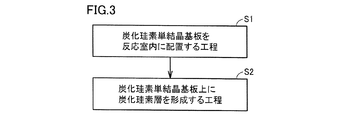
- FIG. 3 is a flowchart schematically showing a method for manufacturing the silicon carbide epitaxial substrate according to the present embodiment.
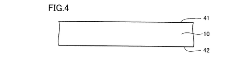
- FIG. 4 is a schematic cross-sectional view showing a first step of the method for manufacturing a silicon carbide epitaxial substrate according to this embodiment.
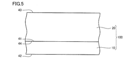
- FIG. 5 is a schematic cross-sectional view showing a second step of the method for manufacturing the silicon carbide epitaxial substrate according to the present embodiment.
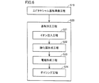
- FIG. 6 is a flowchart schematically showing a method for manufacturing the silicon carbide semiconductor device according to the present embodiment.
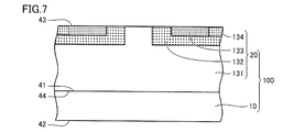
- FIG. 7 is a schematic cross-sectional view showing a first step of the method for manufacturing the silicon carbide semiconductor device according to the present embodiment.
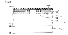
- FIG. 8 is a schematic cross-sectional view showing a second step of the method for manufacturing the silicon carbide semiconductor device according to this embodiment.
- FIG. 9 is a schematic cross-sectional view showing a third step of the method for manufacturing the silicon carbide semiconductor device according to this embodiment.
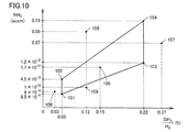
- FIG. 10 is a diagram showing the relationship between the SiH 4 flow rate / H 2 flow rate (%) and the NH 3 flow rate (sccm) in the method for manufacturing a silicon carbide epitaxial substrate according to the evaluation sample.
- the method for manufacturing silicon carbide epitaxial substrate 100 includes the following steps. Silicon carbide single crystal substrate 10 is arranged in reaction chamber 201. By supplying a mixed gas containing silane, ammonia, and hydrogen to reaction chamber 201, silicon carbide layer 20 is formed on silicon carbide single crystal substrate 10. The maximum diameter of silicon carbide single crystal substrate 10 is 100 mm or more. In the step of forming the silicon carbide layer, the first value obtained by dividing the flow rate of silane by the flow rate of hydrogen is expressed as a percentage on the X axis, and the second value expressed in sccm as a second flow rate is used as the Y axis.
- the first value and the second value belong to a rectangular area surrounded by the first coordinate, the second coordinate, the third coordinate, and the fourth coordinate in the XY plane coordinates.
- the first coordinate is (0.05, 6.5 ⁇ 10 ⁇ 4 ).
- the second coordinate is (0.05, 4.5 ⁇ 10 ⁇ 3 ).
- the third coordinate is (0.22, 1.2 ⁇ 10 ⁇ 2 ).
- the fourth coordinate is (0.22, 1.3 ⁇ 10 ⁇ 1 ).
- the average value of the carrier concentration of silicon carbide layer 20 is not less than 1 ⁇ 10 15 cm ⁇ 3 and not more than 2 ⁇ 10 16 cm ⁇ 3 .
- the unit of flow rate “sccm (standard cc / minute)” indicates the flow rate “cc / min” in the standard state (0 ° C., 101.3 kPa).
- a silicon carbide epitaxial substrate used for manufacturing a silicon carbide semiconductor device has an in-plane uniformity of good carrier concentration and a silicon carbide layer while maintaining an average carrier concentration within a certain range required for a silicon carbide semiconductor device. It is required to realize good flatness of the surface. In recent years, in addition to the realization of the above characteristics, it is required to increase the growth rate of the silicon carbide layer.
- concentration of a silicon carbide layer may be unable to satisfy
- silane is used as the source gas
- hydrogen is used as the carrier gas
- ammonia is used as the dopant gas
- the silane flow rate / hydrogen flow rate and the ammonia flow rate are controlled within a certain range.
- the flow rate of silane, the flow rate of hydrogen, so that the value and the second value belong to a rectangular region surrounded by the first coordinate, the second coordinate, the third coordinate, and the fourth coordinate in the XY plane coordinates The flow rate of ammonia is controlled.
- reaction chamber 201 is positioned on first heating region 213 on silicon carbide single crystal substrate 10 and upstream of first heating region 213.
- the second heating region 214 may be included.
- the temperature of second heating region 214 may be equal to or higher than the decomposition temperature of ammonia.
- the length of the second heating region 214 is 60 mm or more in the flow direction of the mixed gas.
- the method for manufacturing the silicon carbide semiconductor device 300 according to the present disclosure includes the following steps.
- a silicon carbide epitaxial substrate manufactured by the method described in any one of (1) to (3) above is prepared.
- a silicon carbide epitaxial substrate is processed.
- Silicon carbide epitaxial substrate 100 manufacturing apparatus 200 includes reaction chamber 201, gas supply unit 235, and control unit 245.
- Reaction chamber 201 is configured to heat silicon carbide single crystal substrate 10.
- the gas supply unit 235 is configured to be able to supply a mixed gas containing silane, ammonia, and hydrogen to the reaction chamber 201.
- the control unit 245 is configured to be able to control the flow rate of the mixed gas supplied from the gas supply unit 235 to the reaction chamber 201.
- the silane flow rate, the ammonia flow rate, and the hydrogen flow rate are such that the value and the second value belong to a rectangular area surrounded by the first coordinate, the second coordinate, the third coordinate, and the fourth coordinate in the XY plane coordinates.
- the flow rate can be controlled.
- the first coordinate is (0.05, 6.5 ⁇ 10 ⁇ 4 ).
- the second coordinate is (0.05, 4.5 ⁇ 10 ⁇ 3 ).
- the third coordinate is (0.22, 1.2 ⁇ 10 ⁇ 2 ).
- the fourth coordinate is (0.22, 1.3 ⁇ 10 ⁇ 1 ).
- reaction chamber 201 includes first heating region 213 and first heating region 213 on the region where silicon carbide single crystal substrate 10 is disposed.
- region 214 located in an upstream rather than may be included.
- region 214 may be comprised so that heating to the temperature more than the decomposition temperature of ammonia is possible.
- the length of the second heating region 214 in the mixed gas flow direction may be 60 mm or more.
- Silicon carbide epitaxial substrate manufacturing equipment The configuration of manufacturing apparatus 200 for silicon carbide epitaxial substrate 100 according to the present embodiment will be described.
- the manufacturing apparatus 200 is, for example, a hot wall type horizontal CVD (Chemical Vapor Deposition) apparatus.
- the manufacturing apparatus 200 mainly includes a reaction chamber 201, a gas supply unit 235, a control unit 245, a heating element 203, a quartz tube 204, a heat insulating material 205, and an induction heating coil 206.
- the heating element 203 has a cylindrical shape, for example, and forms a reaction chamber 201 inside.
- the heating element 203 is made of, for example, graphite.
- the heat insulating material 205 surrounds the outer periphery of the heating element 203.
- the heat insulating material 205 is provided inside the quartz tube 204 so as to contact the inner peripheral surface of the quartz tube 204.
- the induction heating coil 206 is wound, for example, along the outer peripheral surface of the quartz tube 204.
- the induction heating coil 206 is configured to be able to supply an alternating current by an external power source (not shown). Thereby, the heating element 203 is induction-heated. As a result, the reaction chamber 201 is heated by the heating element 203.
- the reaction chamber 201 is a space formed by being surrounded by the heating element 203. Silicon carbide single crystal substrate 10 is arranged in reaction chamber 201. Reaction chamber 201 is configured to heat silicon carbide single crystal substrate 10. The maximum diameter of the silicon carbide single crystal substrate is 100 mm or more. Reaction chamber 201 is provided with a susceptor plate 210 that holds silicon carbide single crystal substrate 10. The susceptor plate 210 is configured to be able to rotate around the rotation shaft 212.
- the manufacturing apparatus 200 further includes a gas introduction port 207 and a gas exhaust port 208.
- the gas exhaust port 208 is connected to an exhaust pump (not shown).
- the arrows in FIG. 1 indicate the gas flow.
- the gas is introduced into the reaction chamber 201 from the gas introduction port 207 and exhausted from the gas exhaust port 208.
- the pressure in the reaction chamber 201 is adjusted by the balance between the gas supply amount and the gas exhaust amount.
- the manufacturing apparatus 200 may further include a heating unit 211 located between the gas inlet 207 and the heating element 203.
- the heating unit 211 is located upstream of the heating element 203.
- the heating element 203 may be configured to be heated to about 1100 ° C. to 1350 ° C., for example.
- the gas supply unit 235 is configured to be able to supply the reaction chamber 201 with a mixed gas containing silane, ammonia, and a gas containing hydrogen and carbon atoms.
- the gas supply unit 235 may include a first gas supply unit 231, a second gas supply unit 232, a third gas supply unit 233, and a carrier gas supply unit 234.
- the first gas supply unit 231 is configured to be able to supply a first gas containing carbon atoms.
- the first gas supply unit 231 is, for example, a gas cylinder filled with the first gas.
- the first gas is, for example, propane (C 3 H 8 ) gas.
- the first gas may be, for example, methane (CH 4 ) gas, ethane (C 2 H 6 ) gas, acetylene (C 2 H 2 ) gas, or the like.
- the second gas supply unit 232 is configured to be able to supply a second gas containing a silane gas.
- the second gas supply unit 232 is, for example, a gas cylinder filled with the second gas.
- the second gas is, for example, silane (SiH 4) gas.
- the second gas may be a mixed gas of silane gas and a gas other than silane.
- the third gas supply unit 233 is configured to be able to supply a third gas containing ammonia gas.
- the third gas supply unit 233 is, for example, a gas cylinder filled with a third gas.
- the third gas is a doping gas containing N (nitrogen atoms). Ammonia gas is more easily pyrolyzed than nitrogen gas having a triple bond. By using ammonia gas, improvement in the in-plane uniformity of the carrier concentration can be expected.
- the carrier gas supply unit 234 is configured to be able to supply a carrier gas such as hydrogen.
- the carrier gas supply unit 234 is a gas cylinder filled with hydrogen, for example.
- the control unit 245 is configured to be able to control the flow rate of the mixed gas supplied from the gas supply unit 235 to the reaction chamber 201.
- the controller 245 may include a first gas flow controller 241, a second gas flow controller 242, a third gas flow controller 243, and a carrier gas flow controller 244. .
- Each control unit may be, for example, an MFC (Mass Flow Controller).
- the control unit 245 is disposed between the gas supply unit 235 and the gas inlet 207. In other words, the control unit 245 is disposed in a flow path that connects the gas supply unit 235 and the gas introduction port 207.
- reaction chamber 201 includes a first heating region 213 on a region where silicon carbide single crystal substrate 10 is disposed, and a second heating region 214 located upstream from first heating region 213. It is out.
- the second heating region 214 has an upstream silicon carbide from the upstream boundary between the heat insulating material 205 and the heating element 203 in the mixed gas flow direction (the axial direction of the reaction chamber 201). This is the region up to the end of the region where the single crystal substrate 10 is disposed.
- the boundary between the second heating region 214 and the first heating region 213 may be the side surface on the upstream side of the recess provided in the susceptor plate 210.
- the downstream end of the first heating region 213 may be a downstream boundary between the heat insulating material 205 and the heating element 203.
- the winding density of the induction heating coil 206 may be changed.
- the winding density [times / m] is the number of coil turns per unit length in the axial direction of the apparatus.
- the winding density of the upstream induction heating coil 206 may be higher than the winding density of the downstream induction heating coil 206. Good.
- the second heating region 214 may be configured to be able to be heated to a temperature equal to or higher than the decomposition temperature of ammonia.
- the decomposition temperature of ammonia is, for example, 500 ° C.
- region 214 is measurable with a radiation thermometer, for example.
- the temperature of the portion of the heating element 203 constituting the second heating region 214 is, for example, 1580 ° C.
- the length 222 of the second heating region 214 may be 60 mm or more, 70 mm or more, 80 mm or more, and preferably 100 mm or less.
- the length 221 of the first heating region 213 may be larger than the length 222 of the second heating region 214.
- the value obtained by dividing the flow rate of silane by the flow rate of hydrogen as a percentage is the X axis, and the flow rate of ammonia is expressed in sccm (second value). Is the Y axis.
- the control unit 245 has a quadrangular region in which the first value (%) and the second value (sccm) are surrounded by the first coordinate, the second coordinate, the third coordinate, and the fourth coordinate in the XY plane coordinates (FIG. 2).
- the flow rate of silane, the flow rate of ammonia, and the flow rate of hydrogen are configured to be controllable so as to belong to the region indicated by hatching in FIG.
- the first coordinates (X1, Y1) are (0.05, 6.5 ⁇ 10 ⁇ 4 ).
- the second coordinate (X2, Y2) is (0.05, 4.5 ⁇ 10 ⁇ 3 ).
- the third coordinate (X3, Y3) is (0.22, 1.2 ⁇ 10 ⁇ 2 ).
- the fourth coordinate (X4, Y4) is (0.22, 1.3 ⁇ 10 ⁇ 1 ).
- the control unit 245 can control, for example, the carrier gas flow rate control unit 244 configured to be controllable so that the flow rate of the carrier gas (hydrogen) becomes 100 slm, and the flow rate of the second gas (silane gas) to 150 sccm. And a third gas flow rate controller 243 configured to be controllable so that the flow rate of the third gas (ammonia gas) is 1.1 ⁇ 10 ⁇ 2 sccm. Including. In this case, the value obtained by dividing the flow rate of silane by the flow rate of hydrogen as a percentage is 0.15%.
- the value obtained by dividing the flow rate of silane by the flow rate of hydrogen (first value) and the value (second value) in which the flow rate of ammonia is expressed in sccm (second value) are indicated by hatching in FIG. Belongs to the area.
- a step of placing a silicon carbide single crystal substrate in the reaction chamber is performed.
- a silicon carbide single crystal of polytype 6H is manufactured by a sublimation method.
- silicon carbide single crystal substrate 10 is prepared by slicing the silicon carbide single crystal with, for example, a wire saw (see FIG. 4).
- Silicon carbide single crystal substrate 10 has a first main surface 41 and a second main surface 42 opposite to the first main surface 41.
- the polytype of the silicon carbide single crystal is, for example, 4H—SiC. 4H—SiC is superior to other polytypes in terms of electron mobility, dielectric breakdown field strength, and the like.
- Silicon carbide single crystal substrate 10 contains an n-type impurity such as nitrogen, for example.
- Silicon carbide single crystal substrate 10 has an n-type conductivity, for example.
- the first main surface 41 is, for example, a surface inclined by an angle of 8 ° or less from the ⁇ 0001 ⁇ plane or the ⁇ 0001 ⁇ plane.
- the first principal surface 41 may be a (0001) plane or a plane inclined by an angle of 8 ° or less from the (0001) plane, or a (000-1) plane or (000-1).
- the surface may be inclined by an angle of 8 ° or less from the surface.
- the inclination direction of the normal line of the first main surface 41 is, for example, the ⁇ 11-20> direction.
- the inclination angle (off angle) from the ⁇ 0001 ⁇ plane may be 1 ° or more, or 2 ° or more.
- the off-angle may be 7 ° or less, 6 ° or less, or 4 ° or less.
- the maximum diameter (diameter) of first main surface 41 of silicon carbide single crystal substrate 10 is 100 mm or more.
- the diameter may be 150 mm or more, 200 mm or more, or 250 mm or more.
- the upper limit of the diameter is not particularly limited, but the upper limit of the diameter may be 300 mm, for example.
- silicon carbide layer 20 is formed by epitaxial growth on silicon carbide single crystal substrate 10 using manufacturing apparatus 200 described above.
- the pressure in the reaction chamber 201 is reduced from atmospheric pressure to about 1 ⁇ 10 ⁇ 6 Pa
- the temperature rise of the silicon carbide single crystal substrate 10 is started.
- hydrogen (H 2 ) gas which is a carrier gas
- the flow rate of hydrogen gas is adjusted by the carrier gas flow rate control unit 244.
- a source gas, a dopant gas, and a carrier gas are supplied to the reaction chamber 201.
- a source gas, a dopant gas, and a carrier gas are supplied to the reaction chamber 201.
- a mixed gas containing silane, ammonia, hydrogen, and propane are supplied to reaction chamber 201.
- each gas is thermally decomposed to form silicon carbide layer 20 on silicon carbide single crystal substrate 10. Is done.
- the C / Si ratio of the mixed gas may be 1.0, for example.
- the value obtained by dividing the flow rate of silane by the flow rate of hydrogen as a percentage is the X axis, and the flow rate of ammonia is expressed in sccm (second value). Is the Y axis.
- the first value and the second value are rectangular regions surrounded by the first coordinate, the second coordinate, the third coordinate, and the fourth coordinate in the XY plane coordinates (hatching in FIG. 2).
- the first coordinates (X1, Y1) are (0.05, 6.5 ⁇ 10 ⁇ 4 ).
- the second coordinate (X2, Y2) is (0.05, 4.5 ⁇ 10 ⁇ 3 ).
- the third coordinate (X3, Y3) is (0.22, 1.2 ⁇ 10 ⁇ 2 ).
- the fourth coordinate (X4, Y4) is (0.22, 1.3 ⁇ 10 ⁇ 1 ).
- the carrier gas flow rate controller 244 is used to adjust the flow rate of the carrier gas (hydrogen) supplied to the reaction chamber 201 to 100 slm.
- the flow rate of the second gas (silane gas) supplied to the reaction chamber 201 is adjusted to 150 sccm.
- the third gas flow rate control unit 243 is used to adjust the flow rate of the third gas (ammonia gas) to 1.1 ⁇ 10 ⁇ 2 sccm. In this case, the value obtained by dividing the flow rate of silane by the flow rate of hydrogen as a percentage is 0.15%.
- the value obtained by dividing the flow rate of silane by the flow rate of hydrogen (first value) and the value (second value) in which the flow rate of ammonia is expressed in sccm (second value) are indicated by hatching in FIG. Belongs to the area.
- the flow rate (sccm) of ammonia may be 6.5 ⁇ 10 ⁇ 4 or more, 4.5 ⁇ 10 ⁇ 3 or more, or 1.1 ⁇ 10 ⁇ 2 or more. It may be 1.2 ⁇ 10 ⁇ 2 or more.
- the flow rate (sccm) of ammonia may be, for example, 1.3 ⁇ 10 ⁇ 1 or less.
- a value (%) obtained by dividing the silane flow rate by the hydrogen flow rate as a percentage (%) may be 0.05 or more, or 0.15 or more.
- a value (%) expressed as a percentage obtained by dividing the flow rate of silane by the flow rate of hydrogen may be 0.22 or less, for example.
- the flow rate of silane may be, for example, 30 sccm or more and 200 sccm or less.
- the flow rate of hydrogen may be, for example, 80 slm or more and 140 slm or less.
- the growth rate of silicon carbide layer 20 may be 8 ⁇ m / h or more, 15 ⁇ m / h or more, 25 ⁇ m / h or more, or 33 ⁇ m / h or more. Good.
- the growth rate of silicon carbide layer 20 may be 50 ⁇ m / h or less.
- the growth rate of the silicon carbide layer 20 can be determined by the flow rate of hydrogen relative to the flow rate of silane. Since silane is a source gas, the growth rate of the silicon carbide layer increases as the flow rate of silane increases. On the other hand, since hydrogen has a property of etching silicon carbide, the growth rate of the silicon carbide layer decreases as the flow rate of hydrogen increases.
- the reaction chamber 201 may include the first heating region 213 on the silicon carbide single crystal substrate 10 and the second heating region 214 located on the upstream side of the first heating region 213.
- the temperature of second heating region 214 may be equal to or higher than the decomposition temperature of ammonia.
- the length of the second heating region 214 may be 60 mm or more.
- silicon carbide layer 20 is formed on silicon carbide single crystal substrate 10 by supplying a mixed gas of silane, propane, ammonia and hydrogen to reaction chamber 201.
- methane (CH 4 ), ethane (C 2 H 6 ), acetylene (C 2 H 2 ), or the like may be used instead of propane.
- the silicon carbide single crystal substrate 10 may rotate around the rotation shaft 212.
- silicon carbide epitaxial substrate 100 see FIG. 5) including silicon carbide single crystal substrate 10 and silicon carbide layer 20 is manufactured.
- Silicon carbide layer 20 has a fourth main surface 44 in contact with silicon carbide single crystal substrate 10 and a third main surface 43 opposite to fourth main surface 44.
- silicon carbide epitaxial substrate 100 manufactured by the above method in-plane uniformity of the carrier concentration in silicon carbide layer 20 is improved while maintaining the average value of the carrier concentration of silicon carbide layer 20 within a certain concentration range. And the root mean square deviation (Sq) of the surface of the silicon carbide layer 20 can be reduced.
- the average value of the carrier concentration of silicon carbide layer 20 is not less than 1 ⁇ 10 15 cm ⁇ 3 and not more than 2 ⁇ 10 16 cm ⁇ 3 .
- the in-plane uniformity of the carrier concentration is, for example, 6% or less.
- the in-plane uniformity of the carrier concentration is a percentage notation of a value obtained by dividing the standard deviation of the carrier concentration by the average value of the carrier concentration.
- the carrier concentration can be measured by, for example, a mercury probe type CV measuring device. Specifically, one probe is arranged on third main surface 43 of silicon carbide layer 20, and the other probe is arranged on second main surface 42 of silicon carbide single crystal substrate 10. The area of one probe is, for example, 0.01 cm 2 .
- a voltage is applied between one probe and the other probe, and the capacitance between one probe and the other probe is measured.
- the vertical axis is 1 / C 2 (reciprocal of the square of capacitance), the horizontal axis is V (voltage), and the carrier concentration is determined from the slope of the straight line of the measurement data.
- the measurement depth of the carrier concentration is adjusted by the applied voltage.
- the carrier concentration in the region of silicon carbide layer 20 that is within about 10 ⁇ m from third main surface 43 toward second main surface 42 is measured.
- the root mean square deviation (Sq) of the third main surface 43 is, for example, 0.4 nm or less.
- the root mean square deviation (Sq) is a parameter obtained by extending the root mean square roughness (Rq) to three dimensions.
- the root mean square deviation (Sq) can be measured, for example, with a white interference microscope.
- the measurement area of the root mean square deviation (Sq) can be a square area with a side of 250 ⁇ m.
- the method for manufacturing a silicon carbide semiconductor device mainly includes an epitaxial substrate preparation step (S10: FIG. 6) and a substrate processing step (S20: FIG. 6).
- an epitaxial substrate preparation step (S10: FIG. 6) is performed. Specifically, silicon carbide epitaxial substrate 100 is prepared by the above-described method for manufacturing a silicon carbide epitaxial substrate (see FIG. 5).
- a substrate processing step (S20: FIG. 6) is performed.
- a silicon carbide semiconductor device is manufactured by processing a silicon carbide epitaxial substrate.
- “Processing” includes, for example, various processes such as ion implantation, heat treatment, etching, oxide film formation, electrode formation, and dicing. That is, the substrate processing step may include at least one of ion implantation, heat treatment, etching, oxide film formation, electrode formation, and dicing.
- the substrate processing step (S20: FIG. 6) includes an ion implantation step (S21: FIG. 6), an oxide film formation step (S22: FIG. 6), an electrode formation step (S23: FIG. 6), and a dicing step (S24: FIG. 6). including.
- an ion implantation step (S21: FIG. 6) is performed.
- a p-type impurity such as aluminum (Al) is implanted into the third main surface 43 on which a mask (not shown) having an opening is formed.
- body region 132 having p-type conductivity is formed.
- an n-type impurity such as phosphorus (P) is implanted into a predetermined position in body region 132.
- a source region 133 having n-type conductivity is formed.
- a p-type impurity such as aluminum is implanted into a predetermined position in the source region 133.
- a contact region 134 having a p-type conductivity is formed (see FIG. 7).
- Source region 133 is separated from drift region 131 by body region 132.
- Ion implantation may be performed by heating silicon carbide epitaxial substrate 100 to about 300 ° C. or more and 600 ° C. or less. After the ion implantation, activation annealing is performed on silicon carbide epitaxial substrate 100. By the activation annealing, the impurities injected into the silicon carbide layer 20 are activated, and carriers are generated in each region.
- the atmosphere of activation annealing may be, for example, an argon (Ar) atmosphere.
- the activation annealing temperature may be about 1800 ° C., for example.
- the activation annealing time may be about 30 minutes, for example.
- oxide film forming step (S22: FIG. 6) is performed.
- silicon carbide epitaxial substrate 100 is heated in an atmosphere containing oxygen, whereby oxide film 136 is formed on third main surface 43 (see FIG. 8).
- Oxide film 136 is made of, for example, silicon dioxide (SiO 2 ).
- the oxide film 136 functions as a gate insulating film.
- the temperature of the thermal oxidation treatment may be about 1300 ° C., for example.
- the thermal oxidation treatment time may be about 30 minutes, for example.
- heat treatment may be performed in a nitrogen atmosphere.
- the heat treatment may be performed at about 1100 ° C. for about 1 hour in an atmosphere such as nitric oxide (NO) or nitrous oxide (N 2 O).
- heat treatment may be performed in an argon atmosphere.
- the heat treatment may be performed in an argon atmosphere at about 1100 to 1500 ° C. for about 1 hour.
- the first electrode 141 is formed on the oxide film 136.
- the first electrode 141 functions as a gate electrode.
- the first electrode 141 is formed by, for example, a CVD method.
- the first electrode 141 is made of, for example, polysilicon containing impurities and having conductivity.
- the first electrode 141 is formed at a position facing the source region 133 and the body region 132.
- Interlayer insulating film 137 covering the first electrode 141 is formed.
- Interlayer insulating film 137 is formed by, for example, a CVD method.
- Interlayer insulating film 137 is made of, for example, silicon dioxide.
- the interlayer insulating film 137 is formed so as to be in contact with the first electrode 141 and the oxide film 136.
- the oxide film 136 and the interlayer insulating film 137 at predetermined positions are removed by etching. As a result, the source region 133 and the contact region 134 are exposed from the oxide film 136.
- the second electrode 142 is formed on the exposed portion by sputtering.
- the second electrode 142 functions as a source electrode.
- Second electrode 142 is made of, for example, titanium, aluminum, silicon, or the like.
- second electrode 142 and silicon carbide epitaxial substrate 100 are heated at a temperature of about 900 to 1100 ° C., for example. Thereby, second electrode 142 and silicon carbide epitaxial substrate 100 come into ohmic contact.
- the wiring layer 138 is formed so as to be in contact with the second electrode 142.
- the wiring layer 138 is made of a material containing aluminum, for example.
- the third electrode 143 is formed on the second main surface 42.
- the third electrode 143 functions as a drain electrode.
- Third electrode 143 is made of, for example, an alloy containing nickel and silicon (eg, NiSi).
- a dicing step (S24: FIG. 6) is performed.
- silicon carbide epitaxial substrate 100 is diced along a dicing line, whereby silicon carbide epitaxial substrate 100 is divided into a plurality of semiconductor chips.
- silicon carbide semiconductor device 300 is manufactured (see FIG. 9).
- the method for manufacturing the silicon carbide semiconductor device according to the present disclosure has been described by exemplifying the MOSFET, but the manufacturing method according to the present disclosure is not limited to this.
- the manufacturing method according to the present disclosure is applicable to various silicon carbide semiconductor devices such as IGBT (Insulated Gate Bipolar Transistor), SBD (Schottky Barrier Diode), thyristor, GTO (Gate Turn Off thyristor), and PiN diode.
- IGBT Insulated Gate Bipolar Transistor
- SBD Schottky Barrier Diode
- thyristor thyristor
- GTO Gate Turn Off thyristor
- PiN diode PiN diode
- the growth rate of the silicon layer is 8 ⁇ m / h.
- the SiH 4 flow rate / H 2 flow rate is 0.22%, and the NH 3 flow rate is 1.2 ⁇ 10 ⁇ 2 ⁇ 20% (sccm).
- the growth rate of the silicon layer is 50 ⁇ m / h.
- the SiH 4 flow rate / H 2 flow rate is 0.22% and the NH 3 flow rate is 1.3 ⁇ 10 ⁇ 1 ⁇ 20% (sccm) in the manufacturing process of the silicon carbide epitaxial substrate according to Sample 4, and the carbonization is performed.
- the growth rate of the silicon layer is 50 ⁇ m / h.
- the SiH 4 flow rate / H 2 flow rate is 0.15%, and the NH 3 flow rate is 1.1 ⁇ 10 ⁇ 2 ⁇ 20% (sccm).
- the growth rate of the silicon layer is 33 ⁇ m / h.
- the SiH 4 flow rate / H 2 flow rate is 0.03%, the NH 3 flow rate is 8 ⁇ 10 ⁇ 4 ⁇ 20% (sccm), and the silicon carbide layer The growth rate is about 2 ⁇ m / h.
- the SiH 4 flow rate / H 2 flow rate is 0.37%, the NH 3 flow rate is 7 ⁇ 10 ⁇ 2 ⁇ 20% (sccm), and the silicon carbide layer The growth rate is 90 ⁇ m / h.
- the SiH 4 flow rate / H 2 flow rate is 0.12%
- the NH 3 flow rate is 9 ⁇ 10 ⁇ 2 ⁇ 20% (sccm)
- the silicon carbide layer The growth rate is 25 ⁇ m / h.
- the SiH 4 flow rate / H 2 flow rate is 0.12%
- the NH 3 flow rate is 1 ⁇ 10 ⁇ 3 ⁇ 20% (sccm)
- the silicon carbide layer The growth rate is 25 ⁇ m / h.
- the H 2 flow rate was 120 slm
- the SiH 4 flow rate was changed to change the SiH 4 flow rate / H 2 flow rate.
- the carrier concentration of silicon carbide layer 20 of silicon carbide epitaxial substrate 100 according to samples 1 to 9 was measured by a mercury probe type CV measuring apparatus.
- the carrier concentration was measured in a region within a radius of 60 mm from the center of the third main surface 43.
- the measurement points of the carrier concentration are a plurality of positions arranged at almost equal intervals on a straight line passing through the center of the third main surface 43 and parallel to the radial direction and a straight line perpendicular to the straight line.
- the measurement position of the carrier concentration is the center of the third main surface 43 and a position away from the center by 10 mm, 20 mm, 30 mm, 40 mm, 50 mm and 60 mm in the radial direction.
- the in-plane uniformity of the carrier concentration was calculated by dividing the standard deviation of the carrier concentration by the average value of the carrier concentration.
- the area of the mercury probe is, for example, 0.01 cm 2 .
- the root mean square deviation (Sq) in the central region of the third main surface 43 was measured.
- the measurement area of the root mean square deviation is a square area with a side of 250 ⁇ m.
- the measurement position of the root mean square deviation is the center of the third main surface 43 and a position 50 mm away from the center in the radial direction.
- Table 1 the range of Sq is shown.
- FIG. 10 is a diagram plotted in XY plane coordinates with SiH 4 / H 2 as the X axis and NH 3 as the Y axis in the manufacturing steps of the silicon carbide epitaxial substrates according to Samples 1 to 9. Coordinates 101 to 109 correspond to the method for manufacturing a silicon carbide epitaxial substrate according to samples 1 to 9, respectively.
- the in-plane uniformity of the carrier concentration in the silicon carbide layers of the silicon carbide epitaxial substrates according to Samples 1 to 9 is less than 6%, less than 6%, less than 3%, and less than 3%, respectively. Less than 2%, about 7%, less than 3%, less than 2% and less than 6%.
- the root mean square deviations (Sq) of the third surfaces of the silicon carbide layers of the silicon carbide epitaxial substrates according to Samples 1 to 9 are 0.1 to 0.4 nm, 0.1 to 0.4 nm, and 0.1 to 0.4, respectively.
- the average carrier concentration in the silicon carbide layer of the silicon carbide epitaxial substrate according to Samples 1 to 9 is 1 ⁇ 10 15 cm ⁇ 3 , 2 ⁇ 10 16 cm ⁇ 3 , 1 ⁇ 10 15 cm ⁇ 3 , 2 ⁇ 10 16 cm. ⁇ 3 , 3 ⁇ 10 15 cm ⁇ 3 , 3 ⁇ 10 15 cm ⁇ 3 , 3 ⁇ 10 15 cm ⁇ 3 , more than 3 ⁇ 10 16 cm ⁇ 3 and less than 1 ⁇ 10 15 cm ⁇ 3 .
- the silicon carbide epitaxial substrates according to Samples 1 to 5 have an average carrier concentration of 1 ⁇ 10 15 cm ⁇ 3 or more and 2 ⁇ 10 16 cm ⁇ 3 or less, and the carrier concentration uniformity value is It was 6% or less, the growth rate was 8 ⁇ m / h or more, and the root mean square deviation (Sq) was 0.4 nm or less. Under the manufacturing conditions of the silicon carbide epitaxial substrate according to Sample 6, the growth rate was 2 ⁇ m / h, and high-speed growth could not be realized. In addition, the silicon carbide epitaxial substrate according to Sample 6 had an in-plane uniformity value of carrier concentration of about 7%, and the carrier concentration was not sufficiently uniform in the plane.
- the silicon carbide epitaxial substrate according to Sample 7 had a root mean square deviation (Sq) larger than 0.8 nm, and the flatness was not sufficiently high.
- the average carrier concentration was larger than 2 ⁇ 10 16 cm ⁇ 3 , and the range of the average carrier concentration required for the power device could not be realized.
- the average carrier concentration was smaller than 1 ⁇ 10 15 cm ⁇ 3 , and the range of average carrier concentration required for the power device could not be realized.
- the silicon carbide epitaxial substrates according to Samples 1 to 5 have good carrier concentration while maintaining the average carrier concentration of 1 ⁇ 10 15 cm ⁇ 3 or more and 2 ⁇ 10 16 cm ⁇ 3 or less. In-plane uniformity, high growth rate, and good flatness were achieved.
- the value obtained by dividing the flow rate of silane by the flow rate of hydrogen (percentage value) and the value (second value) where the flow rate of ammonia is expressed in sccm. The flow rate of silane, hydrogen, and the like so as to belong to a rectangular area (hatched area in FIG.
- silicon carbide single crystal substrate 20 silicon carbide layer, 41 first main surface, 42 second main surface, 43 third main surface, 44 fourth main surface, 100 silicon carbide epitaxial substrate, 131 drift region, 132 body region, 133 source region, 134 contact region, 136 oxide film, 137 interlayer insulating film, 138 wiring layer, 141 first electrode, 142 second electrode, 143 third electrode, 200 manufacturing equipment, 201 reaction chamber, 203 heating element, 204 quartz Pipe, 205 heat insulating material, 206 induction heating coil, 207 gas introduction port, 208 gas exhaust port, 210 susceptor plate, 211 heating unit, 212 rotating shaft, 213 first heating region, 214 second heating region, 221, 222 length 231 1st gas supply part, 232 2nd gas supply part, 233 1st Gas supply unit, 234 carrier gas supply unit, 235 gas supply unit, 241 first gas flow rate control unit, 242 second gas flow rate control unit, 243 third gas flow rate control unit, 244 carrier gas flow rate control unit, 245 control
Landscapes
- Chemical & Material Sciences (AREA)
- Crystallography & Structural Chemistry (AREA)
- Organic Chemistry (AREA)
- Engineering & Computer Science (AREA)
- Materials Engineering (AREA)
- Metallurgy (AREA)
- Chemical Kinetics & Catalysis (AREA)
- General Chemical & Material Sciences (AREA)
- Inorganic Chemistry (AREA)
- Crystals, And After-Treatments Of Crystals (AREA)
- Chemical Vapour Deposition (AREA)
- Recrystallisation Techniques (AREA)
- Carbon And Carbon Compounds (AREA)
Abstract
Description
まず本開示の実施形態について説明する。以下の説明では、同一または対応する要素には同一の符号を付し、それらについて同じ説明は繰り返さない。本明細書の結晶学的記載においては、個別方位を[]、集合方位を<>、個別面を()、集合面を{}でそれぞれ示す。結晶学上の指数が負であることは、通常、数字の上に”-”(バー)を付すことによって表現されるが、本明細書では数字の前に負の符号を付すことによって結晶学上の負の指数を表現する。
以下、本開示の一実施形態(以下「本実施形態」とも記す)について説明する。ただし本実施形態はこれらに限定されるものではない。
本実施形態に係る炭化珪素エピタキシャル基板100の製造装置200の構成について説明する。
次に、本実施形態に係る炭化珪素エピタキシャル基板の製造方法について説明する。
次に、本実施形態に係る炭化珪素半導体装置300の製造方法について説明する。
(サンプル準備)
上述した炭化珪素エピタキシャル基板の製造方法を用いて、サンプル1~9に係る炭化珪素エピタキシャル基板が製造された。サンプル1に係る炭化珪素エピタキシャル基板の製造工程のおける、SiH4流量/H2流量は0.05%であり、NH3流量は6.5×10-4±20%(sccm)であり、炭化珪素層の成長速度は8μm/hである。サンプル2に係る炭化珪素エピタキシャル基板の製造工程のおける、SiH4流量/H2流量は0.05%であり、NH3流量は4.5×10-3±20%(sccm)であり、炭化珪素層の成長速度は8μm/hである。サンプル3に係る炭化珪素エピタキシャル基板の製造工程のおける、SiH4流量/H2流量は0.22%であり、NH3流量は1.2×10-2±20%(sccm)であり、炭化珪素層の成長速度は50μm/hである。サンプル4に係る炭化珪素エピタキシャル基板の製造工程のおける、SiH4流量/H2流量は0.22%であり、NH3流量は1.3×10-1±20%(sccm)であり、炭化珪素層の成長速度は50μm/hである。サンプル5に係る炭化珪素エピタキシャル基板の製造工程のおける、SiH4流量/H2流量は0.15%であり、NH3流量は1.1×10-2±20%(sccm)であり、炭化珪素層の成長速度は33μm/hである。
サンプル1~9に係る炭化珪素エピタキシャル基板100の炭化珪素層20のキャリア濃度が水銀プローブ方式のC-V測定装置により測定された。第3主面43の中心から半径60mm以内の領域において、キャリア濃度が測定された。キャリア濃度の測定箇所は、第3主面43の中心を通り径方向に平行な直線と、当該直線に対して垂直な直線上において、ほぼ等間隔に配置された複数の位置である。具体的には、キャリア濃度の測定位置は、第3主面43の中心と、当該中心から径方向に10mm、20mm、30mm、40mm、50mmおよび60mm離れた位置である。キャリア濃度の測定箇所は、計25箇所である。キャリア濃度の面内均一性は、キャリア濃度の標準偏差をキャリア濃度の平均値で除することにより計算された。なお水銀側のプローブの面積は、たとえば0.01cm2である。
図10は、サンプル1~9に係る炭化珪素エピタキシャル基板の製造工程におけるSiH4/H2をX軸とし、NH3をY軸として、XY平面座標にプロットした図である。座標101~109は、それぞれサンプル1~9に係る炭化珪素エピタキシャル基板の製造方法に対応している。

Claims (7)
- 炭化珪素単結晶基板を反応室内に配置する工程と、
前記反応室に、シランとアンモニアと水素とを含む混合ガスを供給することにより、前記炭化珪素単結晶基板上に炭化珪素層を形成する工程とを備え、
前記炭化珪素単結晶基板の最大径は、100mm以上であり、
前記炭化珪素層を形成する工程において、前記シランの流量を前記水素の流量で除した値を百分率表記した第1値をX軸とし、前記アンモニアの流量をsccmを単位として表記した第2値をY軸としたとき、前記第1値および前記第2値は、XY平面座標における、第1座標、第2座標、第3座標および第4座標に囲まれた四角形の領域内に属し、
前記第1座標は、(0.05,6.5×10-4)であり、
前記第2座標は、(0.05,4.5×10-3)であり、
前記第3座標は、(0.22,1.2×10-2)であり、
前記第4座標は、(0.22,1.3×10-1)であり、
前記炭化珪素層を形成する工程後において、前記炭化珪素層のキャリア濃度の平均値は、1×1015cm-3以上2×1016cm-3以下である、炭化珪素エピタキシャル基板の製造方法。 - 前記反応室は、前記炭化珪素単結晶基板上の第1加熱領域と、前記第1加熱領域よりも上流側に位置する第2加熱領域とを含み、
前記炭化珪素層を形成する工程において、前記第2加熱領域の温度は、アンモニアの分解温度以上である、請求項1に記載の炭化珪素エピタキシャル基板の製造方法。 - 前記混合ガスの流れ方向において、前記第2加熱領域の長さは、60mm以上である、請求項2に記載の炭化珪素エピタキシャル基板の製造方法。
- 請求項1~請求項3のいずれか1項に記載の方法で製造された炭化珪素エピタキシャル基板を準備する工程と、
前記炭化珪素エピタキシャル基板を加工する工程とを備える、炭化珪素半導体装置の製造方法。 - 炭化珪素単結晶基板を加熱可能に構成された反応室と、
前記反応室に、シランとアンモニアと水素とを含む混合ガスを供給可能に構成されたガス供給部と、
前記ガス供給部から前記反応室に供給される前記混合ガスの流量を制御可能に構成された制御部とを備え、
前記制御部は、前記シランの流量を前記水素の流量で除した値を百分率表記した第1値をX軸とし、前記アンモニアの流量をsccmを単位として表記した第2値をY軸としたとき、前記第1値および前記第2値が、XY平面座標における、第1座標、第2座標、第3座標および第4座標に囲まれた四角形の領域内に属するように、前記シランの流量、前記アンモニアの流量および前記水素の流量を制御可能に構成されており、
前記第1座標は、(0.05,6.5×10-4)であり、
前記第2座標は、(0.05,4.5×10-3)であり、
前記第3座標は、(0.22,1.2×10-2)であり、
前記第4座標は、(0.22,1.3×10-1)である、炭化珪素エピタキシャル基板の製造装置。 - 前記反応室は、前記炭化珪素単結晶基板が配置される領域上の第1加熱領域と、前記第1加熱領域よりも上流側に位置する第2加熱領域とを含み、
前記第2加熱領域は、アンモニアの分解温度以上の温度に加熱可能に構成されている、請求項5に記載の炭化珪素エピタキシャル基板の製造装置。 - 前記混合ガスの流れ方向において、前記第2加熱領域の長さは、60mm以上である、請求項6に記載の炭化珪素エピタキシャル基板の製造装置。
Priority Applications (4)
| Application Number | Priority Date | Filing Date | Title |
|---|---|---|---|
| CN201680049960.4A CN107924823B (zh) | 2015-09-29 | 2016-08-02 | 制造碳化硅外延基板的方法、制造碳化硅半导体装置的方法以及制造碳化硅外延基板的设备 |
| JP2016570903A JP6090552B1 (ja) | 2015-09-29 | 2016-08-02 | 炭化珪素エピタキシャル基板の製造方法、炭化珪素半導体装置の製造方法および炭化珪素エピタキシャル基板の製造装置 |
| US15/752,985 US10697086B2 (en) | 2015-09-29 | 2016-08-02 | Method for manufacturing silicon carbide epitaxial substrate, method for manufacturing silicon carbide semiconductor device, and apparatus for manufacturing silicon carbide epitaxial substrate |
| DE112016004430.5T DE112016004430T5 (de) | 2015-09-29 | 2016-08-02 | Verfahren zur Herstellung eines Siliziumkarbid-Epitaxiesubstrats, Verfahren zur Herstellung einer Siliziumkarbid-Halbleitervorrichtung und Vorrichtung zur Herstellung eines Siliziumkarbid-Epitaxiesubstrats |
Applications Claiming Priority (2)
| Application Number | Priority Date | Filing Date | Title |
|---|---|---|---|
| JP2015-191489 | 2015-09-29 | ||
| JP2015191489 | 2015-09-29 |
Publications (1)
| Publication Number | Publication Date |
|---|---|
| WO2017056691A1 true WO2017056691A1 (ja) | 2017-04-06 |
Family
ID=58427377
Family Applications (1)
| Application Number | Title | Priority Date | Filing Date |
|---|---|---|---|
| PCT/JP2016/072625 Ceased WO2017056691A1 (ja) | 2015-09-29 | 2016-08-02 | 炭化珪素エピタキシャル基板の製造方法、炭化珪素半導体装置の製造方法および炭化珪素エピタキシャル基板の製造装置 |
Country Status (5)
| Country | Link |
|---|---|
| US (1) | US10697086B2 (ja) |
| JP (2) | JP6090552B1 (ja) |
| CN (1) | CN107924823B (ja) |
| DE (1) | DE112016004430T5 (ja) |
| WO (1) | WO2017056691A1 (ja) |
Cited By (7)
| Publication number | Priority date | Publication date | Assignee | Title |
|---|---|---|---|---|
| JP2020009940A (ja) * | 2018-07-10 | 2020-01-16 | 住友電気工業株式会社 | 炭化珪素エピタキシャル基板の製造方法および炭化珪素半導体装置の製造方法 |
| WO2020158657A1 (ja) * | 2019-02-01 | 2020-08-06 | 東京エレクトロン株式会社 | 成膜装置及び成膜方法 |
| US11373868B2 (en) | 2018-12-05 | 2022-06-28 | Sumitomo Electric Industries, Ltd. | Method for manufacturing silicon carbide epitaxial substrate |
| US11735415B2 (en) | 2018-08-21 | 2023-08-22 | Sumitomo Electric Industries, Ltd. | Method for manufacturing silicon carbide epitaxial substrate and method for manufacturing silicon carbide semiconductor device |
| US12020927B2 (en) | 2018-08-21 | 2024-06-25 | Sumitomo Electric Industries, Ltd. | Method for manufacturing silicon carbide epitaxial substrate and method for manufacturing silicon carbide semiconductor device |
| JP7651075B1 (ja) * | 2024-08-13 | 2025-03-25 | 住友電気工業株式会社 | 炭化珪素エピタキシャル基板の製造装置、炭化珪素エピタキシャル基板の製造方法、および炭化珪素半導体装置の製造方法 |
| JP7667379B1 (ja) * | 2024-08-13 | 2025-04-22 | 住友電気工業株式会社 | 炭化珪素エピタキシャル基板の製造方法および炭化珪素半導体装置の製造方法 |
Families Citing this family (6)
| Publication number | Priority date | Publication date | Assignee | Title |
|---|---|---|---|---|
| JP7115084B2 (ja) * | 2018-07-10 | 2022-08-09 | 住友電気工業株式会社 | 炭化珪素エピタキシャル基板の製造方法および炭化珪素半導体装置の製造方法 |
| DE102018129492B4 (de) * | 2018-11-22 | 2022-04-28 | Ebner Industrieofenbau Gmbh | Vorrichtung und Verfahren zum Züchten von Kristallen |
| CN110707160B (zh) * | 2019-10-11 | 2021-07-16 | 湖南红太阳光电科技有限公司 | 一种管式直接PECVD制备太阳电池SiC减反射膜的方法 |
| IT202000021517A1 (it) * | 2020-09-11 | 2022-03-11 | Lpe Spa | Metodo per deposizione cvd di carburo di silicio con drogaggio di tipo n e reattore epitassiale |
| KR102283879B1 (ko) * | 2021-01-14 | 2021-07-29 | 에스케이씨 주식회사 | 탄화규소 웨이퍼의 제조방법, 탄화규소 웨이퍼 및 웨이퍼 제조용 시스템 |
| JP2025020907A (ja) * | 2023-07-31 | 2025-02-13 | 株式会社東芝 | 炭化シリコンエピタキシャルウェーハ及びその製造方法 |
Citations (4)
| Publication number | Priority date | Publication date | Assignee | Title |
|---|---|---|---|---|
| JP2006261612A (ja) * | 2005-03-18 | 2006-09-28 | Shikusuon:Kk | 炭化珪素半導体およびその製造方法と製造装置 |
| JP2014154666A (ja) * | 2013-02-07 | 2014-08-25 | Sumitomo Electric Ind Ltd | 炭化珪素半導体基板の製造方法および炭化珪素半導体装置の製造方法 |
| JP2014170891A (ja) * | 2013-03-05 | 2014-09-18 | Sumitomo Electric Ind Ltd | 炭化珪素基板、炭化珪素基板の製造方法および炭化珪素半導体装置の製造方法 |
| JP2014232799A (ja) * | 2013-05-29 | 2014-12-11 | 住友電気工業株式会社 | 炭化珪素半導体基板の製造方法 |
Family Cites Families (4)
| Publication number | Priority date | Publication date | Assignee | Title |
|---|---|---|---|---|
| JP3809464B2 (ja) * | 1999-12-14 | 2006-08-16 | 独立行政法人理化学研究所 | 半導体層の形成方法 |
| US7052546B1 (en) * | 2003-08-28 | 2006-05-30 | Cape Simulations, Inc. | High-purity crystal growth |
| JP6026333B2 (ja) * | 2013-03-25 | 2016-11-16 | 株式会社ニューフレアテクノロジー | 成膜装置および成膜方法 |
| JP2015191489A (ja) | 2014-03-28 | 2015-11-02 | アプリックスIpホールディングス株式会社 | データ書込みシステム及びデータ書込み方法 |
-
2016
- 2016-08-02 JP JP2016570903A patent/JP6090552B1/ja active Active
- 2016-08-02 DE DE112016004430.5T patent/DE112016004430T5/de not_active Withdrawn
- 2016-08-02 CN CN201680049960.4A patent/CN107924823B/zh active Active
- 2016-08-02 US US15/752,985 patent/US10697086B2/en active Active
- 2016-08-02 WO PCT/JP2016/072625 patent/WO2017056691A1/ja not_active Ceased
-
2017
- 2017-01-27 JP JP2017013262A patent/JP2017085169A/ja active Pending
Patent Citations (4)
| Publication number | Priority date | Publication date | Assignee | Title |
|---|---|---|---|---|
| JP2006261612A (ja) * | 2005-03-18 | 2006-09-28 | Shikusuon:Kk | 炭化珪素半導体およびその製造方法と製造装置 |
| JP2014154666A (ja) * | 2013-02-07 | 2014-08-25 | Sumitomo Electric Ind Ltd | 炭化珪素半導体基板の製造方法および炭化珪素半導体装置の製造方法 |
| JP2014170891A (ja) * | 2013-03-05 | 2014-09-18 | Sumitomo Electric Ind Ltd | 炭化珪素基板、炭化珪素基板の製造方法および炭化珪素半導体装置の製造方法 |
| JP2014232799A (ja) * | 2013-05-29 | 2014-12-11 | 住友電気工業株式会社 | 炭化珪素半導体基板の製造方法 |
Cited By (11)
| Publication number | Priority date | Publication date | Assignee | Title |
|---|---|---|---|---|
| JP2020009940A (ja) * | 2018-07-10 | 2020-01-16 | 住友電気工業株式会社 | 炭化珪素エピタキシャル基板の製造方法および炭化珪素半導体装置の製造方法 |
| JP7131146B2 (ja) | 2018-07-10 | 2022-09-06 | 住友電気工業株式会社 | 炭化珪素エピタキシャル基板の製造方法および炭化珪素半導体装置の製造方法 |
| US11735415B2 (en) | 2018-08-21 | 2023-08-22 | Sumitomo Electric Industries, Ltd. | Method for manufacturing silicon carbide epitaxial substrate and method for manufacturing silicon carbide semiconductor device |
| US12020927B2 (en) | 2018-08-21 | 2024-06-25 | Sumitomo Electric Industries, Ltd. | Method for manufacturing silicon carbide epitaxial substrate and method for manufacturing silicon carbide semiconductor device |
| US11373868B2 (en) | 2018-12-05 | 2022-06-28 | Sumitomo Electric Industries, Ltd. | Method for manufacturing silicon carbide epitaxial substrate |
| WO2020158657A1 (ja) * | 2019-02-01 | 2020-08-06 | 東京エレクトロン株式会社 | 成膜装置及び成膜方法 |
| JP7651075B1 (ja) * | 2024-08-13 | 2025-03-25 | 住友電気工業株式会社 | 炭化珪素エピタキシャル基板の製造装置、炭化珪素エピタキシャル基板の製造方法、および炭化珪素半導体装置の製造方法 |
| JP7667379B1 (ja) * | 2024-08-13 | 2025-04-22 | 住友電気工業株式会社 | 炭化珪素エピタキシャル基板の製造方法および炭化珪素半導体装置の製造方法 |
| JP7729504B1 (ja) | 2024-08-13 | 2025-08-26 | 住友電気工業株式会社 | 炭化珪素エピタキシャル基板の製造装置、炭化珪素エピタキシャル基板の製造方法、および炭化珪素半導体装置の製造方法 |
| WO2026038306A1 (ja) * | 2024-08-13 | 2026-02-19 | 住友電気工業株式会社 | 炭化珪素エピタキシャル基板の製造方法および炭化珪素半導体装置の製造方法 |
| JP2026032528A (ja) * | 2024-08-13 | 2026-02-26 | 住友電気工業株式会社 | 炭化珪素エピタキシャル基板の製造装置、炭化珪素エピタキシャル基板の製造方法、および炭化珪素半導体装置の製造方法 |
Also Published As
| Publication number | Publication date |
|---|---|
| US10697086B2 (en) | 2020-06-30 |
| JP2017085169A (ja) | 2017-05-18 |
| CN107924823B (zh) | 2021-09-28 |
| DE112016004430T5 (de) | 2018-07-05 |
| JP6090552B1 (ja) | 2017-03-08 |
| JPWO2017056691A1 (ja) | 2017-10-05 |
| CN107924823A (zh) | 2018-04-17 |
| US20180237942A1 (en) | 2018-08-23 |
Similar Documents
| Publication | Publication Date | Title |
|---|---|---|
| JP6090552B1 (ja) | 炭化珪素エピタキシャル基板の製造方法、炭化珪素半導体装置の製造方法および炭化珪素エピタキシャル基板の製造装置 | |
| JP7052851B2 (ja) | 炭化珪素エピタキシャル基板および炭化珪素半導体装置の製造方法 | |
| JP6696499B2 (ja) | 炭化珪素エピタキシャル基板および炭化珪素半導体装置の製造方法 | |
| JPWO2017138247A1 (ja) | 炭化珪素エピタキシャル基板および炭化珪素半導体装置の製造方法 | |
| JP7371632B2 (ja) | 炭化珪素エピタキシャル基板の製造方法および炭化珪素半導体装置の製造方法 | |
| WO2018142668A1 (ja) | 炭化珪素エピタキシャル基板および炭化珪素半導体装置の製造方法 | |
| JP7415558B2 (ja) | 炭化珪素エピタキシャル基板および炭化珪素半導体装置の製造方法 | |
| JP7310822B2 (ja) | 炭化珪素エピタキシャル基板の製造方法および炭化珪素半導体装置の製造方法 | |
| CN112074928B (zh) | 碳化硅外延衬底和制造碳化硅半导体器件的方法 | |
| JP6954316B2 (ja) | 炭化珪素エピタキシャル基板および炭化珪素半導体装置の製造方法 | |
| WO2017051611A1 (ja) | 炭化珪素エピタキシャル基板の製造方法、炭化珪素半導体装置の製造方法および炭化珪素エピタキシャル基板の製造装置 | |
| JP6791348B2 (ja) | 炭化珪素エピタキシャル基板および炭化珪素半導体装置の製造方法 | |
| JP7131146B2 (ja) | 炭化珪素エピタキシャル基板の製造方法および炭化珪素半導体装置の製造方法 | |
| JP7115084B2 (ja) | 炭化珪素エピタキシャル基板の製造方法および炭化珪素半導体装置の製造方法 |
Legal Events
| Date | Code | Title | Description |
|---|---|---|---|
| ENP | Entry into the national phase |
Ref document number: 2016570903 Country of ref document: JP Kind code of ref document: A |
|
| 121 | Ep: the epo has been informed by wipo that ep was designated in this application |
Ref document number: 16850868 Country of ref document: EP Kind code of ref document: A1 |
|
| WWE | Wipo information: entry into national phase |
Ref document number: 15752985 Country of ref document: US |
|
| WWE | Wipo information: entry into national phase |
Ref document number: 112016004430 Country of ref document: DE |
|
| 122 | Ep: pct application non-entry in european phase |
Ref document number: 16850868 Country of ref document: EP Kind code of ref document: A1 |