WO2017051756A1 - ステッピングモータ駆動装置 - Google Patents
ステッピングモータ駆動装置 Download PDFInfo
- Publication number
- WO2017051756A1 WO2017051756A1 PCT/JP2016/077162 JP2016077162W WO2017051756A1 WO 2017051756 A1 WO2017051756 A1 WO 2017051756A1 JP 2016077162 W JP2016077162 W JP 2016077162W WO 2017051756 A1 WO2017051756 A1 WO 2017051756A1
- Authority
- WO
- WIPO (PCT)
- Prior art keywords
- sine wave
- stepping motor
- generation unit
- unit
- drive current
- Prior art date
- Legal status (The legal status is an assumption and is not a legal conclusion. Google has not performed a legal analysis and makes no representation as to the accuracy of the status listed.)
- Ceased
Links
Images




Classifications
-
- H—ELECTRICITY
- H02—GENERATION; CONVERSION OR DISTRIBUTION OF ELECTRIC POWER
- H02P—CONTROL OR REGULATION OF ELECTRIC MOTORS, ELECTRIC GENERATORS OR DYNAMO-ELECTRIC CONVERTERS; CONTROLLING TRANSFORMERS, REACTORS OR CHOKE COILS
- H02P8/00—Arrangements for controlling dynamo-electric motors rotating step by step
- H02P8/04—Arrangements for starting
Definitions
- the present invention relates to a stepping motor driving device.
- the present invention particularly relates to a stepping motor driving device that suppresses occurrence of a step-out state during an initial operation of a stepping motor.
- a stepping motor driving device includes a digital driving IC (Integrated Circuit), and drives the stepping motor by a driving signal that is a digital signal output from the digital driving IC.
- This drive signal is a waveform in which a stepped waveform and a sawtooth waveform generated by comparing the reference voltage value of the stepped waveform and the feedback voltage value of the coil of the stepping motor are superimposed.
- the stepping motor driving device provided with the digital drive IC particularly when the resolution of the stepped waveform is rough, the frequency of the sawtooth waveform is higher than the frequency of the stepped waveform.
- the stepping motor driving device provided with the digital driving IC has a problem that abnormal noise is generated when the stepping motor is driven.
- an analog drive circuit is provided instead of a digital drive IC.
- a stepping motor driving device including an analog driving circuit is disclosed in Patent Document 1, for example.
- the stepping motor driving device shown in Patent Document 1 includes a filter circuit (sine wave generation unit) including an integration circuit composed of a resistance element and a capacitance element.
- the sine wave generator of the stepping motor driving device disclosed in Patent Document 1 can generate a sine wave by slowing the rise and fall of the stepped waveform of the input step reference voltage.
- the stepping motor driving device disclosed in Patent Document 1 can generate a driving current using a sine wave, there is no need to provide a digital driving IC, and abnormal noise is generated when the stepping motor is driven. It solves the problem that occurs.
- the stepping motor drive device disclosed in Patent Document 1 includes an analog drive circuit, and in particular, the sine wave generation unit includes an integration circuit including a resistance element and a capacitance element. . Therefore, immediately after the input of the step reference voltage, the sine wave generated by the sine wave generator does not become stable due to the time constant determined by the resistance value of the resistance element and the capacitance of the capacitance element.
- the present inventors have recognized that.
- One object of the present invention is to provide a stepping motor driving device that suppresses the occurrence of a step-out state during the initial operation of the stepping motor.
- a first aspect according to the present invention includes a triangular wave generation unit that generates a triangular wave according to an input rectangular wave; A sine wave generating unit that generates a sine wave according to the triangular wave input from the triangular wave generating unit; A drive current generator for generating a drive current for driving the stepping motor according to the sine wave input from the sine wave generator; A control unit for determining whether or not the sine wave generated by the sine wave generation unit is in a stable state; A switch unit provided between the sine wave generation unit and the drive current generation unit; With The control unit enables a switch switching signal when it is determined that the sine wave generated by the sine wave generation unit is in a stable state, while the switch switching is performed when it is not determined as the stable state.
- the switch unit enables input of the sine wave generated by the sine wave generation unit to the drive current generation unit when the switch switching signal is in the enabled state, while the switch switching signal is
- the present invention relates to a stepping motor drive device that does not validate the input of the sine wave generated by the sine wave generation unit to the drive current generation unit when in a disabled state.
- the switch unit since the switch switching signal is enabled by the control unit when the sine wave is in a stable state, the switch unit supplies the sine wave to the drive current generation unit in a stable state. Input is validated.
- the drive current generator When the drive current generator generates a drive current using a sine wave that is in a stable state, the rotation operation of the stepping motor is synchronized with the rectangular wave, and therefore, highly accurate angle control is possible.
- the drive current generator when the drive current generator generates a drive current using a sine wave that is not in a stable state, the rotation operation of the stepping motor is in a step-out state that does not synchronize with the rectangular wave, and therefore highly accurate angle control cannot be performed.
- control unit is configured such that the sine wave is in a stable state when a predetermined time has elapsed since the input of the rectangular wave to the triangular wave generation unit. You may determine that there is.
- the control unit can reliably determine that the sine wave is in a stable state when a predetermined time that is longer than the time required for the sine wave to be in a stable state has elapsed.
- a time from when the switch switching signal is set to the enable state to the present time is set to the enable state to the present time.
- the control unit disables the switching signal when it is determined that the stepping motor is at the mechanical stability point, and does not determine that the stepping motor is at the mechanical stability point May continue the enable state of the switching signal.
- the stepping motor rotates by itself to a mechanical stable point and stops when the supply of drive current is stopped.
- the control unit matches the timing of disabling the switch switching signal with the mechanical stability point of the stepping motor.
- the control unit can match the rotation angle of the stepping motor when the switch switching signal is disabled to the rotation angle at which the stepping motor is actually stopped.
- a sine wave offset unit provided between the sine wave generation unit and the switch unit;
- a bias voltage generator that generates a bias voltage and supplies the bias voltage to the sine wave offset unit and the drive current generator;
- the sine wave offset unit changes the reference voltage level of the sine wave generated by the sine wave generation unit from a ground level to the bias voltage
- the drive current generation unit generates the drive current according to the sine wave in which the reference voltage level is changed by the sine wave offset unit with reference to the bias voltage
- the bias voltage may be a voltage at which a minimum value of the sine wave whose reference voltage level is changed by the sine wave offset unit is equal to or higher than the ground level.
- the drive current generation unit When the sine wave offset unit and the bias voltage generation unit are provided, the drive current generation unit generates the drive current based on the bias voltage, so that the drive current is generated by supplying a positive power supply voltage. Therefore, a negative power supply voltage need not be supplied. Therefore, when the sine wave offset unit and the bias voltage generation unit are provided, the cost, the mounting area, and the like of providing a power supply voltage source for supplying a negative power supply voltage can be reduced as compared with the case where they are not provided. it can.
- FIG. 4A is a graph showing a sine wave generated near the first time point shown in FIG.
- FIG. 4B is a graph showing a sine wave generated near the second time point shown in FIG.
- FIG. 4B is a graph which shows the relationship between progress of time and the torque of the motor shown by FIG.
- FIG. 1 is a time chart which shows the timing which the control part shown by FIG. 1 makes a switch change signal into a disable state.
- FIG. 1 shows an example of the configuration of a stepping motor driving apparatus 10 of the present invention.
- FIG. 2 shows an example of a waveform generated or output at each point shown in FIG.
- the stepping motor driving apparatus 10 includes a control unit 20, a triangular wave generation unit 30, a sine wave generation unit 40, a drive current generation unit 80, and a switch unit 70.
- the stepping motor drive device 10 may further include, for example, a sine wave offset unit 50, a bias voltage generation unit 60, and the like.
- a 4-pole stator is actually arranged 90 degrees apart around the stepping motor 90 (rotor). Then, the two exciting coils are wound around the corresponding pair of pole stators so that the same exciting coil is wound around the opposing pole stators. In this state, a driving current having a phase difference of 90 degrees flows through each excitation coil, whereby the stepping motor 90 (rotor thereof) rotates.
- the control unit 20 includes, for example, a microcomputer having a processing unit, a storage unit, an input / output interface unit, and the like not shown.
- the control unit 20 inputs an ON state or an OFF state of the drive switch 103.
- the drive switch 103 is provided in, for example, a device (not shown) in which the stepping motor 90 is used, and is switched between an ON state and an OFF state by a user operation. Alternatively, the driving switch 103 may be switched between an ON state and an OFF state by another device not shown.
- the control unit 20 outputs the rectangular wave 200 when the ON state of the drive switch 103 is input, for example.
- the rectangular wave 200 has a waveform as shown in FIG. 2 at a point 210 shown in FIG.
- control unit 20 directly outputs the rectangular wave 200.
- control unit 20 may generate a rectangular wave 200 by controlling a rectangular wave generation unit (not shown). Further, the control unit 20 switches the state of the switch switching signal 300 between the enabled state and the disabled state.
- the triangular wave generation unit 30 is, for example, an analog circuit including a differentiation circuit composed of a resistance element and a capacitance element not shown.
- the triangular wave generation unit 30 receives the rectangular wave 200 and generates a triangular wave that is an analog signal according to the rectangular wave 200.
- the triangular wave has a waveform as shown in FIG. 2 at a point 220 shown in FIG. Since the triangular wave generation unit 30 includes a differentiating circuit, it functions as a high-pass filter. As a result, the generated triangular wave includes a positive component and a negative component.
- the sine wave generation unit 40 includes a pseudo sine wave generation circuit 41 and a sine wave generation circuit 46.
- the pseudo sine wave generation circuit 41 is an analog circuit including an integration circuit including a resistance element 42 and a capacitance element 43.
- the sine wave generation circuit 46 is an analog circuit including an integration circuit including a resistance element 47 and a capacitance element 48.
- the capacitive element 43 of the pseudo sine wave generation circuit 41 and the capacitive element 48 of the sine wave generation circuit 46 are connected to the ground 102.
- the pseudo sine wave generation circuit 41 receives a triangular wave and generates a pseudo sine wave that is an analog signal in accordance with the triangular wave.
- the pseudo sine wave has a waveform as shown in FIG. 2 at a point 230 shown in FIG. Since the pseudo sine wave generation circuit 41 includes an integration circuit, it functions as a low-pass filter. As a result, the generated pseudo sine wave has a waveform similar to a sine wave.
- the sine wave generation circuit 46 receives a pseudo sine wave and generates a sine wave that is an analog signal according to the pseudo sine wave.
- the sine wave has a waveform as shown in FIG. 2 at a point 240 shown in FIG. Since the sine wave generation circuit 46 includes an integration circuit, it functions as a low-pass filter. As a result, the generated waveform draws a sine curve.
- the sine wave generation unit 40 generates a sine wave according to the triangular wave input from the triangular wave generation unit 30 as a whole.
- the reference voltage of the sine wave at the point 240 generated by the sine wave generation unit 40 is the ground level (0 V).
- the sine wave offset unit 50 is provided between the sine wave generation unit 40 and the switch unit 70, and is an analog circuit including a differentiation circuit including a resistance element and a capacitance element, not shown.
- the sine wave offset unit 50 inputs a sine wave and changes the reference voltage of the sine wave that is the ground level to the bias voltage supplied from the bias voltage generation unit 60.
- a post-offset sine wave which is a sine wave after the sine wave reference voltage generated by the sine wave generation unit 40 is changed by the sine wave offset unit 50, is shown in FIG. 2 at a point 250 shown in FIG.
- the waveform is as shown.
- the post-offset sine wave has a sine curve with the bias voltage as the reference voltage level.
- the minimum value of the post-offset sine wave is equal to or higher than the ground level.
- the post-offset sine wave is also referred to as a sine wave 250.
- the bias voltage generator 60 is, for example, an analog circuit composed of an operational amplifier and a transistor not shown.
- the bias voltage generator 60 generates a bias voltage that is an analog signal in which the minimum value of the post-offset sine wave is equal to or higher than the ground level.
- the bias voltage generation unit 60 generates, for example, a half voltage of the power supply voltage supplied from the power supply voltage source 101 as the bias voltage. For example, when the power supply voltage source 101 supplies a power supply voltage of 20V, the bias voltage is 10V.
- the switch unit 70 is configured by, for example, a transistor (not shown), and is an analog circuit provided between the drive current generation unit 80 and the sine wave offset unit 50.
- the switch unit 70 enables the sine wave 250 to be input to the drive current generation unit 80 when the switch switching signal 300 input from the control unit 20 is in an enabled state.
- the switch unit 70 does not enable the sine wave 250 to be input to the drive current generation unit 69 when the switch switching signal 300 input from the control unit 20 is in a disabled state.
- the drive current generation unit 80 is an analog circuit configured by, for example, a half bridge circuit, a full bridge circuit, or the like.
- the drive current generation unit 80 operates with reference to half the power supply voltage supplied from the power supply voltage source 101, which is a bias voltage, and corresponds to the input sine wave 250.
- a drive current that is an analog signal is generated.
- the instantaneous value of the drive current generated by the drive current generator 80 increases to the plus side as the instantaneous value of the input sine wave 250 becomes larger than the reference voltage (bias voltage), and the reference voltage (bias As it becomes smaller than (voltage), it becomes larger on the minus side.
- the drive current generator 80 has a drive having a sinusoidal waveform in which the direction and magnitude of the current change with periodicity according to the magnitude of the instantaneous value of the sine wave 250 input with the bias voltage as a reference. Generate current.
- the exciting coil 91 When the drive current flows through the exciting coil 91, the exciting coil 91 is excited, and the stepping motor 90 rotates.
- the stepping motor driving apparatus 10 includes the sine wave offset unit 50 and the bias voltage generation unit 60, so that the drive current generation unit 80 is supplied from the power supply voltage source 101.
- the drive current can be generated only by the positive power supply voltage.
- the stepping motor driving apparatus 10 does not include the sine wave offset unit 50 and the bias voltage generation unit 60, not only a positive power supply voltage is supplied from the power supply voltage source 101 but also from other power supply voltage sources. Negative power supply voltage also needs to be supplied.
- a stepping motor drive device 10 ′ that does not include the sine wave offset unit 50 and the bias voltage generation unit 60 will be described later as a modification.
- FIG. 3 shows the state of the rectangular wave 200 and the switch switching signal 300 over time.
- the time point 0 is a time point when the drive switch 103 is turned on, and is a time point when the input of the rectangular wave 200 to the triangular wave generating unit 30 is started.
- the switch switching signal 300 is in a disabled state.
- the control unit 20 enables the switch switching signal 300 when the stable standby time, which is a predetermined time, has elapsed since the output of the rectangular wave 200 was started.
- a temporary point at which the stable standby time has not elapsed since time point 0 shown in FIG. 3 is defined as a first time point
- a time point when the switch switching signal 300 is enabled by the control unit 20 is defined as a second time point.
- FIG. 4A shows the waveform of the sine wave 250 near the first time point shown in FIG.
- FIG. 4B shows the waveform of the sine wave 250 near the second time point shown in FIG.
- the waveform of the sine wave 250 shown in FIG. 4A is not a sine curve based on the reference voltage (bias voltage), and the sine wave 250 is not in a stable state.
- the waveform of the sine wave 250 shown in FIG. 4B is a sine curve based on the reference voltage, and the sine wave 250 is in a stable state.
- the time required for the sine wave 250 to be in a stable state after the output of the rectangular wave 200 is started by the control unit 20 is due to the fact that the stepping motor driving apparatus 10 includes an analog circuit.
- the pseudo sine wave generation circuit 41 and the sine wave generation circuit 46 which are the sine wave generation unit 40, include an integration circuit composed of a resistance element and a capacitance element, so that the resistance value of the resistance element and the capacitance of the capacitance element The fixed time constant has an effect.
- the length of the stable standby time shown in FIG. 3 is determined in consideration of the time constant in the analog circuit of the stepping motor driving apparatus 10, particularly the sine wave generator 40.
- FIG. 5 shows the relationship between the passage of time and the motor torque of the stepping motor 90 when it is assumed that the control unit 20 has enabled the switch switching signal 300 at time 0.
- the motor torque is included in the step-out operation region. That is, assuming that the control unit 20 has enabled the switch switching signal 300 near the first time point, the step-out state is a state in which the rotation operation of the stepping motor 90 is not synchronized with the rectangular wave 200 output by the control unit 20. Therefore, highly accurate angle control cannot be performed. This is because when the driving current is generated using the sine wave 250 that is not in a stable state, for example, the direction and magnitude of the driving current does not change with periodicity, and thus the motor torque of the stepping motor 90 cannot be obtained sufficiently. is there.
- the motor torque is included in the normal operation region. That is, assuming that the control unit 20 enables the switch switching signal 300 near the second time point, the rotational operation of the stepping motor 90 is in a state of being synchronized with the rectangular wave 200 output by the control unit 20, and the accuracy High angle control is possible.
- the sine wave 250 is in a stable state
- the drive current generation unit 80 generates a drive current using the sine wave 250
- the rectangular wave 200 output by the control unit 20 is converted into the rectangular wave 200 output from the stepping motor 90. Rotating motion is synchronized.
- the stable standby time shown in FIG. 3 is determined to be a time longer than the time until the sine wave 250 becomes stable. That is, the control unit 20 determines that the sine wave 250 is in a stable state when the stable standby time has elapsed from the time when the output of the rectangular wave 200 is started (time 0). As a result, the control unit 20 can reliably determine that the sine wave 250 is in a stable state. On the other hand, the control unit 20 determines that the sine wave 250 is not in a stable state when the stable standby time has not elapsed since the time when the output of the rectangular wave 200 was started (time 0). 3 and 4, the instantaneous value of the sine wave 250 at the second time point shown as the time point when the stable standby time has elapsed is shown to be the minimum value. It is not necessary to set in consideration of the instantaneous value of the wave 250.
- FIG. 6 shows the state of the sine wave 250 and the switch switching signal 300 over time.
- the control unit 20 can grasp the progress of the sine wave 250 by counting the effective time, which is the elapsed time from the time when the switch switching signal is enabled. Further, when a drive current corresponding to the sine wave 250 flows through the exciting coil 91 of the stepping motor 90, the progress of the sine wave 250 corresponds to the rotation angle of the stepping motor 90.
- the stepping motor 90 has a mechanical stable point.
- the mechanical stable point of the stepping motor 90 is a rotation angle at which the stepping motor 90 (rotor) stops without rotating when no drive current is supplied to the exciting coil 91 of the stepping motor 90.
- 24 mechanical stable points of the stepping motor 90 exist during one rotation of the stepping motor 90.
- the rotation angle of the stepping motor 90 coincides with the mechanical stable point every time the waveform of the sine wave 250 advances or returns by x ⁇ (x is a positive integer).
- the switch switching signal 300 is enabled by the control unit 20 at the second time point. Thereby, the sine wave 250 is valid for input to the drive current generator 60 from the second time point.
- the control unit 20 inputs that the drive switch 103 has been turned off. If the control unit 20 disables the switch switching signal 300 at the third time point, no drive current is supplied to the exciting coil 91 of the stepping motor 90 at the third time point. However, the stepping motor 90 does not stop at the rotation angle at the third time point, but stops by rotating to the next mechanical stable point. As a result, there is a possibility that a deviation occurs between the rotation angle of the stepping motor 90 when the control unit 20 disables the switch switching signal 300 and the rotation angle at which the stepping motor 90 is actually stopped.
- the control unit 20 is the time from when the control unit 20 enables the switch switching signal 300 to the present when the drive switch 103 is turned off. , Refer to the valid time. Based on this valid time, the control unit 20 determines whether or not the waveform of the sine wave 250 is advanced by x ⁇ . When the control unit 20 determines that the waveform of the sine wave 250 is advanced by x ⁇ , the control unit 20 disables the switch switching signal 300. On the other hand, when it is determined that the waveform of the sine wave 250 is not advanced by x ⁇ , the control unit 20 disables the switch switching signal 300 when the waveform of the sine wave 250 is advanced by x ⁇ thereafter. To.
- the waveform of the sine wave 250 is not advanced by x ⁇ at the third time point when the control unit 20 inputs that the drive switch 103 is turned off. Therefore, the control unit 20 waits until the fourth time point when the waveform of the sine wave 250 is advanced by x ⁇ , and disables the switch switching signal 300.
- the switch switching signal 300 is disabled when the stepping motor 90 rotates to the mechanical stable point.
- the rotation angle of the stepping motor 90 at the time when the controller 20 disables the switch switching signal 300 matches the rotation angle at which the stepping motor 90 is actually stopped. That is, for example, the control unit 20 can acquire an accurate rotation angle when the stepping motor 90 is actually stopped.
- the switch switching signal is immediately after the waveform of the sine wave 250 is advanced by x ⁇ .
- 300 is disabled.
- the control unit 20 may stop the output of the rectangular wave 200 at the same time when the switch switching signal 300 is disabled or after the switch switching signal 300 is disabled.
- step S01 for example, when the ON state of the drive switch 103 is input, the control unit 20 outputs the rectangular wave 200.
- the rectangular wave 200 passes through the triangular wave generation unit 30, the sine wave generation unit 40, and the sine wave offset unit 50 to generate the sine wave 250.
- step S02 the control unit 20 determines whether or not the sine wave 250 is in a stable state.
- the control unit 20 determines that the sine wave 250 is in a stable state
- the flow proceeds to step S03.
- the determination in step S02 is repeated.
- step S03 the control unit 20 enables the switch switching signal 300.
- the switch switching signal 300 When the switch switching signal 300 is enabled, the input of the sine wave 250 to the drive current generator 80 becomes valid, and the drive current generated by the drive current generator 80 is supplied to the excitation coil 91 of the stepping motor 90. . As a result, the stepping motor 90 rotates.
- step S04 the control unit 20 determines whether or not the drive switch 103 is in an OFF state, for example.
- the control unit 20 determines that the drive switch 103 is in the OFF state
- the flow proceeds to step S05.
- the control unit 20 determines that the drive switch 103 is not in the OFF state, that is, in the ON state
- the determination in step S04 is repeated.
- step S05 the control unit 20 determines whether or not the current rotation angle of the stepping motor 90 is a mechanical stable point.
- the control unit 20 determines that the current rotation angle of the stepping motor 90 is a mechanical stable point.
- the flow proceeds to step S06.
- the control unit 20 determines that the current rotation angle of the stepping motor 90 is not a mechanical stable point, the determination in step S05 is repeated.
- step S06 the control unit 20 disables the switch switching signal 300.
- the control unit 20 disables the switch switching signal 300
- the input of the sine wave 250 to the drive current generation unit 80 becomes invalid, and no drive current is generated by the drive current generation unit 80. The rotation stops.
- step S07 the control unit 20 stops the output of the rectangular wave 200.
- the control unit 20 stops outputting the rectangular wave 200 the sine wave 250 is not generated.
- Step S07 may be executed simultaneously with step S06, or after step S06. When the process of step S07 is executed, the flow ends.
- FIG. 8 shows a configuration example of a stepping motor driving device 10 ′, which is a modification of the stepping motor driving device 10 shown in FIG.
- a stepping motor driving device 10 ′ which is a modification of the stepping motor driving device 10 shown in FIG.
- the description of the stepping motor drive device 10 ′ only the portions different from the stepping motor drive device 10 will be described, and the description of the same portions will be omitted.
- the sine wave offset unit 50 and the bias voltage generation unit 60 in the stepping motor driving device 10 shown in FIG. That is, in the stepping motor driving apparatus 10 ′, the sine wave reference voltage generated by the sine wave generation unit 40 is not changed.
- the sine wave generated by the sine wave generation unit 40 which is the sine wave (240 points) shown in FIG. Input to the unit 80.
- the sine wave generated by the sine wave generation unit 40 which is the sine wave (240 points) shown in FIG.
- the drive current generator 80 operates with reference to the ground level voltage (0 V), and generates a drive current according to the input sine wave 240. That is, as shown in FIG. 8, in the stepping motor driving apparatus 10 ′, not only the positive power supply voltage is supplied from the power supply voltage source 101 but also the negative power supply voltage needs to be supplied from the power supply voltage source 104. is there.
- the drive current generation unit 80 supplies not only the positive power supply voltage but also the negative power supply voltage in order to generate the drive current. Need to be done. Therefore, the stepping motor driving device 10 including the sine wave offset unit 50 and the bias voltage generation unit 60 supplies a negative power supply voltage as compared with the case where the sine wave offset unit 50 and the bias voltage generation unit 60 are not provided. The cost and mounting area of the power supply voltage source 107 can be reduced.
- the present invention can be used for a stepping motor driving device.
- SYMBOLS 10 ... Stepping motor drive device, 20 ... Control part, 30 ... Triangle wave generation part, 40 ... Sine wave generation part, 41 ... Pseudo sine wave generation circuit, 46 ... Sine wave generation Circuit: 50 ... Sine wave offset unit, 60 ... Bias voltage generation unit, 70 ... Switch unit, 80 ... Drive current generation unit, 90 ... Stepping motor, 91 ... Excitation coil, 200 ... rectangular wave, 300 ... switch switching signal.
Landscapes
- Engineering & Computer Science (AREA)
- Power Engineering (AREA)
- Control Of Stepping Motors (AREA)
Abstract
ステッピングモータの初期動作時に脱調状態が発生することを抑制するステッピングモータ駆動装置を提供する。 ステッピングモータ駆動装置10は、三角波生成部30と、正弦波生成部40と、駆動電流生成部80と、制御部20と、スイッチ部70と、を備える。制御部20は、正弦波が安定状態であると判定したときはスイッチ切替信号300をイネーブル状態にする一方で、安定状態であると判定しないときはスイッチ切替信号300をディスイネーブル状態にする。スイッチ部70は、スイッチ切替信号300がイネーブル状態であるときは正弦波の駆動電流生成部80への入力を有効にする一方で、スイッチ切替信号300がディスイネーブル状態であるときは正弦波の駆動電流生成部80への入力を有効にしない。
Description
本発明は、ステッピングモータ駆動装置に関する。本発明は、特に、ステッピングモータの初期動作時に脱調状態が発生することを抑制するステッピングモータ駆動装置に関する。
従来、ステッピングモータ駆動装置は、デジタル駆動IC(Integrated Circuit)を備え、このデジタル駆動ICから出力されるデジタル信号である駆動信号によりステッピングモータを駆動させるものである。この駆動信号は、ステップ状の波形と、このステップ状の波形の基準電圧値とステッピングモータのコイルのフィードバック電圧値との比較により生成される鋸状の波形と、が重畳した波形である。
ここで、デジタル駆動ICを備えるステッピングモータ駆動装置では、特に、ステップ状の波形の分解能が粗いときに、ステップ状の波形の周波数より鋸状の波形の周波数の方が高くなる。その結果、デジタル駆動ICを備えるステッピングモータ駆動装置では、ステッピングモータの駆動の際に異音が発生する問題点があった。
この問題を解決するために、例えば、デジタル駆動ICを備える代わりに、アナログ駆動回路を備えることが考えられている。アナログ駆動回路を備えるステッピングモータ駆動装置は、例えば、特許文献1に示されている。
特許文献1に示されているステッピングモータ駆動装置は、抵抗素子及び容量素子で構成される積分回路を含むフィルタ回路(正弦波生成部)を備える。特許文献1に示されているステッピングモータ駆動装置の正弦波生成部は、入力するステップ基準電圧のステップ状の波形の立ち上り及び立ち下がりを緩やかにすることによって、正弦波を生成することができる。その結果、特許文献1に示されているステッピングモータ駆動装置は、正弦波を用いて駆動電流を生成することができるため、デジタル駆動ICを備える必要がなく、ステッピングモータの駆動の際に異音が発生する問題点を解決している。
ところで、特許文献1に示されているステッピングモータ駆動装置は、上述したように、アナログ駆動回路が備えられており、特に、正弦波生成部は抵抗素子及び容量素子で構成される積分回路を含む。そのため、ステップ基準電圧の入力開始直後は、抵抗素子の抵抗値及び容量素子の静電容量で定まる時定数の大きさに起因して、正弦波生成部によって生成される正弦波が安定状態にならないことを、本発明者らは認識した。
このように、特許文献1に示されているステッピングモータ駆動装置では、ステップ基準電圧の入力開始直後は、駆動電流の生成に安定状態の正弦波を用いることができない。したがって、特許文献1に示されているステッピングモータ駆動装置では、ステッピングモータの初期動作時に、ステッピングモータの回転動作が入力信号であるステップ基準電圧に同期しない状態である、脱調状態が発生するおそれがあることを本発明者らは認識した。
本発明の1つの目的は、ステッピングモータの初期動作時に脱調状態が発生することを抑制するステッピングモータ駆動装置を提供することにある。本発明の他の目的は、以下に例示する態様及び好ましい実施形態、並びに添付の図面を参照することによって、当業者に明らかになるであろう。
本発明に従う第1の態様は、入力する矩形波に応じて三角波を生成する三角波生成部と、
前記三角波生成部から入力する前記三角波に応じて正弦波を生成する正弦波生成部と、
前記正弦波生成部から入力する前記正弦波に応じてステッピングモータを駆動する駆動電流を生成する駆動電流生成部と、
前記正弦波生成部が生成する前記正弦波が安定状態であるか否かを判定する制御部と、
前記正弦波生成部と前記駆動電流生成部との間に設けられるスイッチ部と、
を備え、
前記制御部は、前記正弦波生成部が生成する前記正弦波が安定状態であると判定したときはスイッチ切替信号をイネーブル状態にする一方で、前記安定状態であると判定しないときは前記スイッチ切替信号をディスイネーブル状態にし、
前記スイッチ部は、前記スイッチ切替信号が前記イネーブル状態であるときは前記正弦波生成部が生成する前記正弦波の前記駆動電流生成部への入力を有効にする一方で、前記スイッチ切替信号が前記ディスイネーブル状態であるときは前記正弦波生成部が生成する前記正弦波の前記駆動電流生成部への入力を有効にしないステッピングモータ駆動装置に関する。
前記三角波生成部から入力する前記三角波に応じて正弦波を生成する正弦波生成部と、
前記正弦波生成部から入力する前記正弦波に応じてステッピングモータを駆動する駆動電流を生成する駆動電流生成部と、
前記正弦波生成部が生成する前記正弦波が安定状態であるか否かを判定する制御部と、
前記正弦波生成部と前記駆動電流生成部との間に設けられるスイッチ部と、
を備え、
前記制御部は、前記正弦波生成部が生成する前記正弦波が安定状態であると判定したときはスイッチ切替信号をイネーブル状態にする一方で、前記安定状態であると判定しないときは前記スイッチ切替信号をディスイネーブル状態にし、
前記スイッチ部は、前記スイッチ切替信号が前記イネーブル状態であるときは前記正弦波生成部が生成する前記正弦波の前記駆動電流生成部への入力を有効にする一方で、前記スイッチ切替信号が前記ディスイネーブル状態であるときは前記正弦波生成部が生成する前記正弦波の前記駆動電流生成部への入力を有効にしないステッピングモータ駆動装置に関する。
第1の態様のステッピングモータ駆動装置は、正弦波が安定状態であるときに制御部によってスイッチ切替信号がイネーブル状態にされるため、スイッチ部によって安定状態である正弦波の駆動電流生成部への入力が有効にされる。安定状態である正弦波を用いて駆動電流生成部が駆動電流を生成することによって、ステッピングモータの回転動作が矩形波に同期するため、精度の高い角度制御が可能となる。言い換えると、安定状態でない正弦波を用いて駆動電流生成部が駆動電流を生成した場合は、ステッピングモータの回転動作が矩形波に同期しない脱調状態となるため、精度の高い角度制御ができない。
本発明に従う第2の態様では、第1の態様において、前記制御部は、前記三角波生成部に前記矩形波が入力を開始した時点から所定時間が経過したときに、この正弦波が安定状態であると判定してもよい。
矩形波が入力されてから、正弦波が安定状態になるまでには、時間を要する。これは、ステッピングモータ駆動装置がアナログ回路を備えているため、アナログ回路に含まれる抵抗素子及び容量素子による時定数が影響していることによる。正弦波が安定状態になるまでに要する時間以上の所定時間が経過したときに、制御部は正弦波が安定状態であることを確実に判定することができる。
本発明に従う第3の態様では、第1又は第2の態様において、前記制御部は、前記ステッピングモータの駆動を停止するときに、前記スイッチ切替信号を前記イネーブル状態にした時点から現在までの時間を参照して、前記ステッピングモータの機械的な安定点であるか否かを判定し、
前記制御部は、前記ステッピングモータの前記機械的な安定点であると判定したときに前記切替信号をディスイネーブル状態にする一方で、前記ステッピングモータの前記機械的な安定点であると判定しないときは前記切替信号のイネーブル状態を継続してもよい。
前記制御部は、前記ステッピングモータの前記機械的な安定点であると判定したときに前記切替信号をディスイネーブル状態にする一方で、前記ステッピングモータの前記機械的な安定点であると判定しないときは前記切替信号のイネーブル状態を継続してもよい。
ステッピングモータは、駆動電流の供給が停止されたときに、機械的な安定点まで自身で回転して停止する。ここで、制御部は、スイッチ切替信号をディスイネーブル状態にするタイミングを、ステッピングモータの機械的な安定点と一致させる。その結果、制御部は、スイッチ切替信号をディスイネーブル状態にした時点でのステッピングモータの回転角度と、実際にステッピングモータが停止した回転角度とを一致させることができる。
本発明に従う第4の態様では、第1から第3の態様において、前記正弦波生成部と前記スイッチ部との間に設けられる正弦波オフセット部と、
バイアス電圧を発生させて、このバイアス電圧を前記正弦波オフセット部及び前記駆動電流生成部へ供給するバイアス電圧発生部と、
をさらに備え、
前記正弦波オフセット部は、前記正弦波生成部によって生成された前記正弦波の基準電圧レベルを、グランドレベルから前記バイアス電圧へ変更し、
前記駆動電流生成部は、前記バイアス電圧を基準にして、前記正弦波オフセット部によって前記基準電圧レベルが変更された前記正弦波に応じて前記駆動電流を生成し、
前記バイアス電圧は、前記正弦波オフセット部によって前記基準電圧レベルが変更された前記正弦波の最小値が前記グランドレベル以上になる電圧であってもよい。
バイアス電圧を発生させて、このバイアス電圧を前記正弦波オフセット部及び前記駆動電流生成部へ供給するバイアス電圧発生部と、
をさらに備え、
前記正弦波オフセット部は、前記正弦波生成部によって生成された前記正弦波の基準電圧レベルを、グランドレベルから前記バイアス電圧へ変更し、
前記駆動電流生成部は、前記バイアス電圧を基準にして、前記正弦波オフセット部によって前記基準電圧レベルが変更された前記正弦波に応じて前記駆動電流を生成し、
前記バイアス電圧は、前記正弦波オフセット部によって前記基準電圧レベルが変更された前記正弦波の最小値が前記グランドレベル以上になる電圧であってもよい。
正弦波オフセット部及びバイアス電圧発生部が備えられているときは、バイアス電圧を基準に駆動電流生成部が駆動電流を生成するため、プラスの電源電圧が供給されることによって駆動電流を生成することができ、マイナスの電源電圧が供給される必要がない。したがって、正弦波オフセット部及びバイアス電圧発生部を備える場合は、これらを備えない場合と比較して、マイナスの電源電圧を供給するための電源電圧源を設けるコスト及び実装面積等を削減することができる。
以下に説明する好ましい実施形態は、本発明を容易に理解するために用いられている。従って、当業者は、本発明が、以下に説明される実施形態によって不当に限定されないことを留意すべきである。
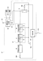
図1及び図2を用いて、本発明のステッピングモータ駆動装置10の構成の例と、図1に示される各地点で生成又は出力される波形の例を説明する。図1には、本発明のステッピングモータ駆動装置10の構成の例が示されている。図2には、図1に示される各地点で生成又は出力される波形の例が示されている。
ステッピングモータ駆動装置10は、制御部20と、三角波生成部30と、正弦波生成部40と、駆動電流生成部80と、スイッチ部70と、を備える。ステッピングモータ駆動装置10は、例えば、正弦波オフセット部50、バイアス電圧発生部60等をさらに備えてもよい。
なお、ステッピングモータ90は、例えば2相励磁方式である場合、実際には、4極の固定子が、ステッピングモータ90(の回転子)の周りに90度ずつ離れて配置される。そして、対抗する極の固定子に同一の励磁コイルが巻かれるように、2つの励磁コイルが各々対応する一対の極の固定子に巻かれる。この状態で、各励磁コイルに90度の位相差を持った駆動電流が流れることによってステッピングモータ90(の回転子)が回転する。
しかしながら、以下の説明においては、説明を簡明にするために、2つの励磁コイルのうち一対の固定子に巻かれた励磁コイル91のみを駆動する内容として説明する。すなわち、実際は、三角波生成部30、正弦波生成部40及び正弦波オフセット部50はそれぞれ2つずつ備えられるが、図1においてこれらは1つずつのみ図示されている。また、実際には、これらによって、90度の位相差を有する2つの矩形波から90度の位相差を有する2つの正弦波が生成されるが、以下の説明では、このうち一方についてのみ説明する。
制御部20は、例えば、図示されていない処理部、記憶部及び入出力インターフェース部等を有するマイクロコンピュータから構成されている。制御部20は、駆動スイッチ103のON状態又はOFF状態を入力する。駆動スイッチ103は、例えば、ステッピングモータ90が用いられる図示されていない装置等に設けられ、ユーザーの操作によってON状態又はOFF状態が切り替わるものである。代替的に、駆動スイッチ103は、図示されていない他の装置等によってON状態又はOFF状態が切り替えられてもよい。
制御部20は、例えば、駆動スイッチ103のON状態を入力したときに、矩形波200を出力する。矩形波200は、例えば、図1に示される地点210において、図2に示されるような波形となる。
また、制御部20が直接矩形波200を出力する場合に限られず、例えば、制御部20が、図示されていない矩形波生成部等を制御して矩形波200を生成させてもよい。また、制御部20は、スイッチ切替信号300の状態をイネーブル状態とディスイネーブル状態との間で切り替える。
三角波生成部30は、例えば、図示されていない抵抗素子及び容量素子からなる微分回路を含むアナログ回路である。三角波生成部30は、矩形波200を入力し、矩形波200に応じてアナログ信号である三角波を生成する。この三角波は、例えば、図1に示される地点220において、図2に示されるような波形となる。三角波生成部30が微分回路を有することによって、ハイパスフィルタとして機能する。その結果、生成される三角波は、正成分及び負成分を含む。
正弦波生成部40は、擬似正弦波生成回路41と正弦波生成回路46とから構成される。擬似正弦波生成回路41は、抵抗素子42及び容量素子43からなる積分回路を含むアナログ回路である。正弦波生成回路46は、抵抗素子47及び容量素子48からなる積分回路を含むアナログ回路である。擬似正弦波生成回路41の容量素子43及び正弦波生成回路46の容量素子48は、グランド102に接続されている。
擬似正弦波生成回路41は、三角波を入力し、三角波に応じてアナログ信号である擬似正弦波を生成する。擬似正弦波は、例えば、図1に示される地点230において、図2に示されるような波形となる。擬似正弦波生成回路41が積分回路を有することによって、ローパスフィルタとして機能する。その結果、生成される擬似正弦波は、正弦波に似た波形となる。
正弦波生成回路46は、擬似正弦波を入力し、擬似正弦波に応じてアナログ信号である正弦波を生成する。正弦波は、例えば、図1に示される地点240において、図2に示されるような波形となる。正弦波生成回路46が積分回路を有することによって、ローパスフィルタとして機能する。その結果、生成される波形は、正弦曲線を描く。
すなわち、正弦波生成部40は、全体として、三角波生成部30から入力する三角波に応じて正弦波を生成する。また、正弦波生成部40によって生成される地点240における正弦波の基準電圧は、グランドレベル(0V)である。
正弦波オフセット部50は、正弦波生成部40とスイッチ部70との間に設けられ、例えば図示されていない抵抗素子及び容量素子からなる微分回路を含むアナログ回路である。正弦波オフセット部50は、正弦波を入力し、グランドレベルである正弦波の基準電圧を、バイアス電圧発生部60から供給されるバイアス電圧へ変更する。
正弦波生成部40が生成した正弦波の基準電圧が、正弦波オフセット部50によって変更された後の正弦波であるオフセット後正弦波は、例えば、図1に示される地点250において、図2に示されるような波形となる。図2に示されるように、オフセット後正弦波は、バイアス電圧を基準電圧レベルとして正弦曲線を描いている。また、図2に示されるように、オフセット後正弦波の最小値がグランドレベル以上となっている。以下、オフセット後正弦波を正弦波250とも呼ぶ。
バイアス電圧発生部60は、例えば、図示されていないオペアンプとトランジスタ等によって構成されているアナログ回路である。バイアス電圧発生部60は、オフセット後正弦波の最小値がグランドレベル以上となるアナログ信号であるバイアス電圧を発生させる。バイアス電圧発生部60は、例えば、電源電圧源101から供給される電源電圧の半分の電圧をバイアス電圧として発生させる。例えば、電源電圧源101が20Vの電源電圧を供給しているとき、バイアス電圧は10Vである。
スイッチ部70は、例えば図示されていないトランジスタ等によって構成され、駆動電流生成部80と正弦波オフセット部50との間に設けられているアナログ回路である。スイッチ部70は、制御部20から入力するスイッチ切替信号300がイネーブル状態であるときに、正弦波250が駆動電流生成部80へ入力することを有効にする。その一方で、スイッチ部70は、制御部20から入力するスイッチ切替信号300がディスイネーブル状態であるときは、正弦波250が駆動電流生成部69へ入力することを有効にしない。
駆動電流生成部80は、例えば、ハーフブリッジ回路、フルブリッジ回路等によって構成されているアナログ回路である。駆動電流生成部80は、図1に示される例においては、バイアス電圧である、電源電圧源101から供給される電源電圧の半分の電圧を基準にして動作し、入力する正弦波250に応じてアナログ信号である駆動電流を生成する。例えば、駆動電流生成部80によって生成される駆動電流の瞬時値は、入力する正弦波250の瞬時値が、基準電圧(バイアス電圧)より大きくなるに応じてプラス側に大きくなり、基準電圧(バイアス電圧)より小さくなるに応じてマイナス側に大きくなる。
すなわち、駆動電流生成部80は、バイアス電圧を基準に入力する正弦波250の瞬時値の大きさに応じて、電流の向き及び大きさが周期性を持って変化する正弦波状の波形を有する駆動電流を生成する。駆動電流が励磁コイル91に流れることによって、励磁コイル91が励磁され、ステッピングモータ90が回転動作する。
このように、図1に示される構成の例においては、ステッピングモータ駆動装置10が正弦波オフセット部50及びバイアス電圧発生部60を備えることによって、駆動電流生成部80は、電源電圧源101から供給されるプラスの電源電圧のみで、駆動電流を生成することができる。言い換えると、ステッピングモータ駆動装置10が、正弦波オフセット部50及びバイアス電圧発生部60を備えないときは、電源電圧源101からプラスの電源電圧が供給されるだけでなく、他の電源電圧源からマイナスの電源電圧も供給される必要がある。なお、正弦波オフセット部50及びバイアス電圧発生部60を備えないステッピングモータ駆動装置10'は、変形例として後述する。
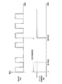
図3、図4及び図5を用いて、ステッピングモータ駆動装置10の制御部20がスイッチ切替信号300をイネーブル状態にするタイミングを説明する。図3には、時間の経過に応じた矩形波200及びスイッチ切替信号300の状態が示されている。
図3に示される時間軸の左端である時点0は、例えば、制御部20が矩形波200の出力を開始した時点である。すなわち、時点0は、駆動スイッチ103がON状態になった時点であり、三角波生成部30に矩形波200の入力が開始された時点である。
図3に示されるように、時点0では、スイッチ切替信号300はディスイネーブル状態である。図3に示されるように、制御部20は、矩形波200の出力を開始してから、所定時間である安定待機時間が経過したときに、スイッチ切替信号300をイネーブル状態にしている。ここで、図3に示される、時点0から安定待機時間が経過していない一時点を第1時点とし、制御部20によってスイッチ切替信号300がイネーブル状態にされた時点を第2時点とする。
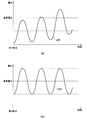
図4(a)には、図3に示される第1時点付近の正弦波250の波形が示されている。図4(b)には、図3に示される第2時点付近の正弦波250の波形が示されている。図4(a)に示される正弦波250の波形は、基準電圧(バイアス電圧)を基準とした正弦曲線となっておらず、正弦波250が安定状態となっていない。その一方で、図4(b)に示される正弦波250の波形は、基準電圧を基準とした正弦曲線となっており、正弦波250が安定状態となっている。
このように、制御部20によって矩形波200の出力が開始されてから、正弦波250が安定状態になるまで時間を要するのは、ステッピングモータ駆動装置10がアナログ回路を備えていることに起因する。特に、正弦波生成部40である擬似正弦波生成回路41及び正弦波生成回路46が、抵抗素子及び容量素子からなる積分回路を含むことによって、抵抗素子の抵抗値及び容量素子の静電容量によって定まる時定数が影響している。
すなわち、ステッピングモータ駆動装置10のアナログ回路、特に正弦波生成部40における時定数が大きくなるに応じて、正弦波250が安定状態になるまでの時間が長くなる。したがって、図3に示される安定待機時間の長さは、ステッピングモータ駆動装置10のアナログ回路、特に正弦波生成部40における時定数を考慮して決定される。
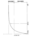
図5には、制御部20が、時点0でスイッチ切替信号300をイネーブル状態にしたと仮定したときの、時間の経過とステッピングモータ90のモータトルクとの関係が示されている。図5に示されるように、第1時点付近では、モータトルクが脱調動作領域に含まれている。すなわち、第1時点付近で、制御部20がスイッチ切替信号300をイネーブル状態にしたと仮定すると、制御部20が出力する矩形波200にステッピングモータ90の回転動作が同期しない状態である脱調状態が発生するため、精度の高い角度制御ができない。これは、安定状態でない正弦波250を用いて駆動電流を生成すると、例えば駆動電流の向き及び大きさが周期性を持って変化しないため、ステッピングモータ90のモータトルクが十分に得られないためである。
その一方で、図5に示されるように、第2時点付近では、モータトルクが正常動作領域に含まれている。すなわち、第2時点付近で、制御部20がスイッチ切替信号300をイネーブル状態にしたと仮定すると、ステッピングモータ90の回転動作が、制御部20が出力する矩形波200に同期する状態であり、精度の高い角度制御が可能となる。このように、正弦波250が安定状態になることによって、駆動電流生成部80がその正弦波250を用いて駆動電流を生成したときに、制御部20が出力する矩形波200にステッピングモータ90の回転動作が同期する。
このように、図3に示されている安定待機時間は、正弦波250が安定状態になるまでの時間以上の時間に決定される。すなわち、制御部20は、矩形波200の出力を開始した時点(時点0)から安定待機時間が経過したときに、正弦波250が安定状態であると判定する。その結果、制御部20は、正弦波250が安定状態であることを確実に判定することができる。その一方で、制御部20は、矩形波200の出力を開始した時点(時点0)から安定待機時間が経過していないときは、正弦波250が安定状態でないと判定する。なお、図3及び図4において、安定待機時間が経過した時点として示されている第2時点における正弦波250の瞬時値は最小値であるように示されているが、安定待機時間は、正弦波250の瞬時値を考慮して設定される必要はない。
図6を用いて、ステッピングモータ駆動装置10の制御部20がスイッチ切替信号300をディスイネーブル状態にするタイミングを説明する。図6には、時間の経過に応じた正弦波250及びスイッチ切替信号300の状態が示されている。
制御部20は、スイッチ切替信号をイネーブル状態にした時点からの経過時間である、有効時間をカウントすることによって、正弦波250の進み具合を把握することができる。また、正弦波250に応じた駆動電流がステッピングモータ90の励磁コイル91に流れることによって、正弦波250の進み具合とステッピングモータ90の回転角度は対応する。
ここで、ステッピングモータ90には、機械的な安定点が存在し、ステッピングモータ90が回転を停止するときは、必ず機械的な安定点で停止する。ステッピングモータ90の機械的な安定点とは、ステッピングモータ90の励磁コイル91に駆動電流が供給されていないときに、ステッピングモータ90(の回転子)が回転しないで停止する回転角度である。ステッピングモータ90の機械的な安定点は、ステッピングモータ90が1回転する間に例えば24箇所存在する。以下の説明において、正弦波250の波形がxπ(xは正の整数)進む又は戻る毎に、ステッピングモータ90の回転角度が、機械的な安定点と一致するものとする。
図6に示されているタイムチャートでは、第2時点で、制御部20によってスイッチ切替信号300がイネーブル状態にされている。それによって、正弦波250は、第2時点から駆動電流生成部60への入力が有効になっている。
例えば、図6に示されている第3時点で、制御部20が、駆動スイッチ103がOFF状態になったことを入力したと仮定する。仮に、第3時点で制御部20がスイッチ切替信号300をディスイネーブル状態にしたとすると、第3時点でステッピングモータ90の励磁コイル91には駆動電流が供給されなくなる。しかしながら、ステッピングモータ90は、第3時点の回転角度では停止せず、次の機械的な安定点まで自身で回転して停止する。その結果、制御部20がスイッチ切替信号300をディスイネーブル状態にした時点でのステッピングモータ90の回転角度と、実際にステッピングモータ90が停止した回転角度とにズレが生じる可能性がある。
このことを防止するために、制御部20は、駆動スイッチ103がOFF状態になったことを入力したときに、制御部20がスイッチ切替信号300をイネーブル状態にした時点から現在までの時間である、有効時間を参照する。制御部20は、この有効時間に基づいて、正弦波250の波形がxπ進んだ状態であるか否かを判定する。制御部20は、正弦波250の波形がxπ進んだ状態であると判定したときは、スイッチ切替信号300をディスイネーブル状態にする。その一方で、制御部20は、正弦波250の波形がxπ進んだ状態でないと判定したときは、その後に正弦波250の波形がxπ進んだ状態となる時点でスイッチ切替信号300をディスイネーブル状態にする。
図6に示される例を参照すると、制御部20が、駆動スイッチ103がOFF状態になったことを入力した時点である第3時点では、正弦波250の波形がxπ進んだ状態でない。そのため、制御部20は、正弦波250の波形がxπ進んだ状態となった第4時点まで待機してスイッチ切替信号300をディスイネーブル状態にしている。
このように、制御部20は、駆動スイッチ103がOFF状態になったことを入力すると、ステッピングモータ90が機械的な安定点まで回転したときにスイッチ切替信号300をディスイネーブル状態にする。その結果、制御部20がスイッチ切替信号300をディスイネーブル状態にした時点でのステッピングモータ90の回転角度と、実際にステッピングモータ90が停止した回転角度とが一致する。すなわち、制御部20は、例えば、実際にステッピングモータ90が停止した時点の正確な回転角度を取得することができる。
なお、図6に示されるように、制御部20が、正弦波250の波形がxπ進んだ状態でないと判定した直後の、正弦波250の波形がxπ進んだ状態となる時点で、スイッチ切替信号300をディスイネーブル状態にすることが好ましい。その結果、駆動スイッチ103がOFF状態になった時点と、実際にステッピングモータ90が停止する時点とのズレが小さくなる。また、制御部20は、スイッチ切替信号300をディスイネーブル状態にすると同時に、又は、スイッチ切替信号300をディスイネーブル状態にした後に、矩形波200の出力を停止してもよい。
図7に示されるフローチャートを用いて、本発明のステッピングモータ駆動装置10の制御部20の一連の動作の例を説明する。ステップS01では、制御部20は、例えば、駆動スイッチ103のON状態を入力したときに、矩形波200を出力する。上述したように、この矩形波200が三角波生成部30、正弦波生成部40及び正弦波オフセット部50を通ることによって正弦波250が生成される。
ステップS02では、制御部20は、正弦波250が安定状態であるか否かを判定する。制御部20が、正弦波250が安定状態であると判定したときは、フローはステップS03に進む。その一方で、正弦波250が安定状態でないと判定したときは、ステップS02の判定を繰り返す。
ステップS03では、制御部20は、スイッチ切替信号300をイネーブル状態にする。スイッチ切替信号300がイネーブル状態になると、正弦波250の駆動電流生成部80への入力が有効になり、駆動電流生成部80で生成される駆動電流がステッピングモータ90の励磁コイル91に供給される。その結果、ステッピングモータ90が回転する。
ステップS04では、制御部20は、例えば駆動スイッチ103がOFF状態であるか否かを判定する。制御部20が、駆動スイッチ103がOFF状態であると判定したときは、フローはステップS05に進む。その一方で、制御部20が、駆動スイッチ103がOFF状態でない、すなわちON状態であると判定したときは、ステップS04の判定を繰り返す。
ステップS05では、制御部20は、現時点のステッピングモータ90の回転角度が機械的な安定点であるか否かを判定する。制御部20が、現時点のステッピングモータ90の回転角度が機械的な安定点であると判定したときは、フローはステップS06に進む。その一方で、制御部20が、現時点のステッピングモータ90の回転角度が機械的な安定点でないと判定したときは、ステップS05の判定を繰り返す。
ステップS06では、制御部20は、スイッチ切替信号300をディスイネーブル状態にする。制御部20がスイッチ切替信号300をディスイネーブル状態にすると、正弦波250の駆動電流生成部80への入力が無効になり、駆動電流生成部80で駆動電流が生成されなくなるため、ステッピングモータ90の回転が停止する。
ステップS07では、制御部20は、矩形波200の出力を停止する。制御部20が矩形波200の出力を停止すると、正弦波250が生成されなくなる。ステップS07は、ステップS06と同時に実行されてもよく、ステップS06の後でもよい。ステップS07の処理が実行されると、フローは終了する。
図8を用いて、本発明のステッピングモータ駆動装置10の変形例を説明する。図8には、図1に示されるステッピングモータ駆動装置10の変形例であるステッピングモータ駆動装置10'の構成例が示されている。ステッピングモータ駆動装置10'の説明は、ステッピングモータ駆動装置10と異なる部分のみ説明し、同じ部分については説明を省略する。
図8に示されるステッピングモータ駆動装置10'には、図1に示されるステッピングモータ駆動装置10における正弦波オフセット部50及びバイアス電圧発生部60が備えられていない。すなわち、ステッピングモータ駆動装置10'では、正弦波生成部40によって生成された正弦波の基準電圧が変更されない。
その結果、制御部20によってスイッチ切替信号300がイネーブル状態にされたときに、図2に示される正弦波(240地点)である、正弦波生成部40によって生成された正弦波が、駆動電流生成部80に入力される。以下、図2に示される正弦波(240地点)である正弦波生成部40によって生成された正弦波を、正弦波240とも呼ぶ。
また、バイアス電圧発生部60が備えられていないことによって、駆動電流生成部80は、グランドレベルの電圧(0V)を基準にして動作し、入力する正弦波240に応じて駆動電流を生成する。すなわち、図8に示されるように、ステッピングモータ駆動装置10'では、電源電圧源101からプラスの電源電圧が供給されるだけでなく、電源電圧源104からマイナスの電源電圧が供給される必要がある。
このように、正弦波オフセット部50及びバイアス電圧発生部60が備えられていないときは、駆動電流生成部80が駆動電流を生成するために、プラスの電源電圧だけでなくマイナスの電源電圧が供給される必要がある。したがって、正弦波オフセット部50及びバイアス電圧発生部60を備えるステッピングモータ駆動装置10は、正弦波オフセット部50及びバイアス電圧発生部60を備えない場合と比較して、マイナスの電源電圧を供給するための電源電圧源107を設けるコスト及び実装面積等を削減することができる。
なお、すでに説明したステッピングモータ駆動装置10の説明で用いられた「正弦波250」は、ステッピングモータ駆動装置10'に関しては「正弦波240」と読み換えられる。
本発明は、上述の例示的な実施形態に限定されず、また、当業者は、上述の例示的な実施形態を特許請求の範囲に含まれる範囲まで、容易に変更することができるであろう。
本発明は、ステッピングモータ駆動装置に利用できる。
10・・・ステッピングモータ駆動装置、20・・・制御部、30・・・三角波生成部、40・・・正弦波生成部、41・・・擬似正弦波生成回路、46・・・正弦波生成回路、50・・・正弦波オフセット部、60・・・バイアス電圧発生部、70・・・スイッチ部、80・・・駆動電流生成部、90・・・ステッピングモータ、91・・・励磁コイル、200・・・矩形波、300・・・スイッチ切替信号。
Claims (4)
- 入力する矩形波に応じて三角波を生成する三角波生成部と、
前記三角波生成部から入力する前記三角波に応じて正弦波を生成する正弦波生成部と、
前記正弦波生成部から入力する前記正弦波に応じてステッピングモータを駆動する駆動電流を生成する駆動電流生成部と、
前記正弦波生成部が生成する前記正弦波が安定状態であるか否かを判定する制御部と、
前記正弦波生成部と前記駆動電流生成部との間に設けられるスイッチ部と、
を備え、
前記制御部は、前記正弦波生成部が生成する前記正弦波が安定状態であると判定したときはスイッチ切替信号をイネーブル状態にする一方で、前記安定状態であると判定しないときは前記スイッチ切替信号をディスイネーブル状態にし、
前記スイッチ部は、前記スイッチ切替信号が前記イネーブル状態であるときは前記正弦波生成部が生成する前記正弦波の前記駆動電流生成部への入力を有効にする一方で、前記スイッチ切替信号が前記ディスイネーブル状態であるときは前記正弦波生成部が生成する前記正弦波の前記駆動電流生成部への入力を有効にしないステッピングモータ駆動装置。 - 前記制御部は、前記三角波生成部に前記矩形波が入力を開始した時点から所定時間が経過したときに、この正弦波が安定状態であると判定する、請求項1に記載のステッピングモータ駆動装置。
- 前記制御部は、前記ステッピングモータの駆動を停止するときに、前記スイッチ切替信号を前記イネーブル状態にした時点から現在までの時間を参照して、前記ステッピングモータの機械的な安定点であるか否かを判定し、
前記制御部は、前記ステッピングモータの前記機械的な安定点であると判定したときに前記切替信号をディスイネーブル状態にする一方で、前記ステッピングモータの前記機械的な安定点であると判定しないときは前記切替信号のイネーブル状態を継続する、請求項1又は2に記載のステッピングモータ駆動装置。 - 前記正弦波生成部と前記スイッチ部との間に設けられる正弦波オフセット部と、
バイアス電圧を発生させて、このバイアス電圧を前記正弦波オフセット部及び前記駆動電流生成部へ供給するバイアス電圧発生部と、
をさらに備え、
前記正弦波オフセット部は、前記正弦波生成部によって生成された前記正弦波の基準電圧レベルを、グランドレベルから前記バイアス電圧へ変更し、
前記駆動電流生成部は、前記バイアス電圧を基準にして、前記正弦波オフセット部によって前記基準電圧レベルが変更された前記正弦波に応じて前記駆動電流を生成し、
前記バイアス電圧は、前記正弦波オフセット部によって前記基準電圧レベルが変更された前記正弦波の最小値が前記グランドレベル以上になる電圧である、請求項1から3のいずれか1項に記載のステッピングモータ駆動装置。
Priority Applications (1)
| Application Number | Priority Date | Filing Date | Title |
|---|---|---|---|
| JP2017541528A JP6729594B2 (ja) | 2015-09-24 | 2016-09-14 | ステッピングモータ駆動装置 |
Applications Claiming Priority (2)
| Application Number | Priority Date | Filing Date | Title |
|---|---|---|---|
| JP2015186883 | 2015-09-24 | ||
| JP2015-186883 | 2015-09-24 |
Publications (1)
| Publication Number | Publication Date |
|---|---|
| WO2017051756A1 true WO2017051756A1 (ja) | 2017-03-30 |
Family
ID=58386776
Family Applications (1)
| Application Number | Title | Priority Date | Filing Date |
|---|---|---|---|
| PCT/JP2016/077162 Ceased WO2017051756A1 (ja) | 2015-09-24 | 2016-09-14 | ステッピングモータ駆動装置 |
Country Status (2)
| Country | Link |
|---|---|
| JP (1) | JP6729594B2 (ja) |
| WO (1) | WO2017051756A1 (ja) |
Citations (4)
| Publication number | Priority date | Publication date | Assignee | Title |
|---|---|---|---|---|
| JPH09103096A (ja) * | 1995-10-05 | 1997-04-15 | Canon Inc | ステッピングモータの駆動装置 |
| JPH09172797A (ja) * | 1995-11-16 | 1997-06-30 | Deutsche Thomson Brandt Gmbh | 同期モータの動作用のディジタルコントローラを有する回路 |
| JP2008181000A (ja) * | 2007-01-25 | 2008-08-07 | Kyocera Mita Corp | モータ駆動制御装置及び画像形成装置 |
| JP2009095127A (ja) * | 2007-10-09 | 2009-04-30 | Seiko Epson Corp | ステッピングモーターの制御 |
-
2016
- 2016-09-14 JP JP2017541528A patent/JP6729594B2/ja active Active
- 2016-09-14 WO PCT/JP2016/077162 patent/WO2017051756A1/ja not_active Ceased
Patent Citations (4)
| Publication number | Priority date | Publication date | Assignee | Title |
|---|---|---|---|---|
| JPH09103096A (ja) * | 1995-10-05 | 1997-04-15 | Canon Inc | ステッピングモータの駆動装置 |
| JPH09172797A (ja) * | 1995-11-16 | 1997-06-30 | Deutsche Thomson Brandt Gmbh | 同期モータの動作用のディジタルコントローラを有する回路 |
| JP2008181000A (ja) * | 2007-01-25 | 2008-08-07 | Kyocera Mita Corp | モータ駆動制御装置及び画像形成装置 |
| JP2009095127A (ja) * | 2007-10-09 | 2009-04-30 | Seiko Epson Corp | ステッピングモーターの制御 |
Also Published As
| Publication number | Publication date |
|---|---|
| JP6729594B2 (ja) | 2020-07-22 |
| JPWO2017051756A1 (ja) | 2018-07-12 |
Similar Documents
| Publication | Publication Date | Title |
|---|---|---|
| CN111049433B (zh) | 磁极初始位置检测装置以及磁极位置检测装置 | |
| JP5917294B2 (ja) | モータ駆動回路 | |
| JP6841336B2 (ja) | モータの制御装置及び記憶媒体 | |
| JP5668947B2 (ja) | モータ駆動制御装置、モータ駆動制御方法及びそれを用いたモータ | |
| JP5709933B2 (ja) | 逆起電力検出回路およびそれを用いたモーター駆動制御装置 | |
| WO2005083876A1 (ja) | モータ駆動装置及びモータを有する電気機器 | |
| JP6329504B2 (ja) | モータ駆動制御装置およびモータ駆動制御方法 | |
| JP6313186B2 (ja) | モータ駆動制御装置及びモータ駆動制御装置の制御方法 | |
| JP4706344B2 (ja) | 同期モータの制御装置 | |
| JP2018170880A (ja) | 電動機駆動装置、方法、及びプログラム | |
| KR20140070210A (ko) | 모터 구동 제어 장치, 모터 구동 제어 방법 및 그를 이용한 모터 | |
| JP6729594B2 (ja) | ステッピングモータ駆動装置 | |
| WO2019021663A1 (ja) | モータ駆動制御装置及びモータの駆動制御方法 | |
| JP2015228723A (ja) | モータ制御装置 | |
| JP6133177B2 (ja) | モータ駆動制御装置及びモータ駆動制御装置の制御方法 | |
| CN107078679B (zh) | 电力转换装置和电力转换装置的控制方法 | |
| JP6674420B2 (ja) | モータ駆動制御装置 | |
| JP6082681B2 (ja) | モータ駆動制御装置及びモータ駆動制御装置の制御方法 | |
| WO2018186061A1 (ja) | ポンプ制御装置 | |
| JP2016171707A (ja) | モータ駆動制御装置及びモータ制御システム | |
| JP2017184427A (ja) | モータの駆動回路および起動方法、プリンタ装置 | |
| JP7004143B2 (ja) | モータ制御装置 | |
| JP2017195659A (ja) | 電子制御装置及びモータ制御装置 | |
| JP5082586B2 (ja) | 交流電動機の制御方法 | |
| JP2008236814A (ja) | モータのpwm制御回路 |
Legal Events
| Date | Code | Title | Description |
|---|---|---|---|
| 121 | Ep: the epo has been informed by wipo that ep was designated in this application |
Ref document number: 16848544 Country of ref document: EP Kind code of ref document: A1 |
|
| ENP | Entry into the national phase |
Ref document number: 2017541528 Country of ref document: JP Kind code of ref document: A |
|
| NENP | Non-entry into the national phase |
Ref country code: DE |
|
| 122 | Ep: pct application non-entry in european phase |
Ref document number: 16848544 Country of ref document: EP Kind code of ref document: A1 |