WO2017047604A1 - 複合基板の製造方法 - Google Patents
複合基板の製造方法 Download PDFInfo
- Publication number
- WO2017047604A1 WO2017047604A1 PCT/JP2016/077032 JP2016077032W WO2017047604A1 WO 2017047604 A1 WO2017047604 A1 WO 2017047604A1 JP 2016077032 W JP2016077032 W JP 2016077032W WO 2017047604 A1 WO2017047604 A1 WO 2017047604A1
- Authority
- WO
- WIPO (PCT)
- Prior art keywords
- piezoelectric substrate
- substrate
- thickness
- peripheral portion
- polishing pad
- Prior art date
- Legal status (The legal status is an assumption and is not a legal conclusion. Google has not performed a legal analysis and makes no representation as to the accuracy of the status listed.)
- Ceased
Links
Images




Classifications
-
- H—ELECTRICITY
- H10—SEMICONDUCTOR DEVICES; ELECTRIC SOLID-STATE DEVICES NOT OTHERWISE PROVIDED FOR
- H10N—ELECTRIC SOLID-STATE DEVICES NOT OTHERWISE PROVIDED FOR
- H10N30/00—Piezoelectric or electrostrictive devices
- H10N30/01—Manufacture or treatment
- H10N30/08—Shaping or machining of piezoelectric or electrostrictive bodies
- H10N30/085—Shaping or machining of piezoelectric or electrostrictive bodies by machining
- H10N30/086—Shaping or machining of piezoelectric or electrostrictive bodies by machining by polishing or grinding
-
- B—PERFORMING OPERATIONS; TRANSPORTING
- B24—GRINDING; POLISHING
- B24B—MACHINES, DEVICES, OR PROCESSES FOR GRINDING OR POLISHING; DRESSING OR CONDITIONING OF ABRADING SURFACES; FEEDING OF GRINDING, POLISHING, OR LAPPING AGENTS
- B24B37/00—Lapping machines or devices; Accessories
- B24B37/04—Lapping machines or devices; Accessories designed for working plane surfaces
- B24B37/07—Lapping machines or devices; Accessories designed for working plane surfaces characterised by the movement of the work or lapping tool
- B24B37/10—Lapping machines or devices; Accessories designed for working plane surfaces characterised by the movement of the work or lapping tool for single side lapping
-
- B—PERFORMING OPERATIONS; TRANSPORTING
- B81—MICROSTRUCTURAL TECHNOLOGY
- B81C—PROCESSES OR APPARATUS SPECIALLY ADAPTED FOR THE MANUFACTURE OR TREATMENT OF MICROSTRUCTURAL DEVICES OR SYSTEMS
- B81C1/00—Manufacture or treatment of devices or systems in or on a substrate
- B81C1/00436—Shaping materials, i.e. techniques for structuring the substrate or the layers on the substrate
- B81C1/00555—Achieving a desired geometry, i.e. controlling etch rates, anisotropy or selectivity
- B81C1/00611—Processes for the planarisation of structures
-
- H—ELECTRICITY
- H03—ELECTRONIC CIRCUITRY
- H03H—IMPEDANCE NETWORKS, e.g. RESONANT CIRCUITS; RESONATORS
- H03H3/00—Apparatus or processes specially adapted for the manufacture of impedance networks, resonating circuits, resonators
- H03H3/007—Apparatus or processes specially adapted for the manufacture of impedance networks, resonating circuits, resonators for the manufacture of electromechanical resonators or networks
- H03H3/08—Apparatus or processes specially adapted for the manufacture of impedance networks, resonating circuits, resonators for the manufacture of electromechanical resonators or networks for the manufacture of resonators or networks using surface acoustic waves
-
- H—ELECTRICITY
- H10—SEMICONDUCTOR DEVICES; ELECTRIC SOLID-STATE DEVICES NOT OTHERWISE PROVIDED FOR
- H10N—ELECTRIC SOLID-STATE DEVICES NOT OTHERWISE PROVIDED FOR
- H10N30/00—Piezoelectric or electrostrictive devices
- H10N30/01—Manufacture or treatment
- H10N30/07—Forming of piezoelectric or electrostrictive parts or bodies on an electrical element or another base
- H10N30/072—Forming of piezoelectric or electrostrictive parts or bodies on an electrical element or another base by laminating or bonding of piezoelectric or electrostrictive bodies
-
- H—ELECTRICITY
- H10—SEMICONDUCTOR DEVICES; ELECTRIC SOLID-STATE DEVICES NOT OTHERWISE PROVIDED FOR
- H10N—ELECTRIC SOLID-STATE DEVICES NOT OTHERWISE PROVIDED FOR
- H10N30/00—Piezoelectric or electrostrictive devices
- H10N30/01—Manufacture or treatment
- H10N30/08—Shaping or machining of piezoelectric or electrostrictive bodies
- H10N30/085—Shaping or machining of piezoelectric or electrostrictive bodies by machining
- H10N30/088—Shaping or machining of piezoelectric or electrostrictive bodies by machining by cutting or dicing
-
- H—ELECTRICITY
- H10—SEMICONDUCTOR DEVICES; ELECTRIC SOLID-STATE DEVICES NOT OTHERWISE PROVIDED FOR
- H10N—ELECTRIC SOLID-STATE DEVICES NOT OTHERWISE PROVIDED FOR
- H10N30/00—Piezoelectric or electrostrictive devices
- H10N30/704—Piezoelectric or electrostrictive devices based on piezoelectric or electrostrictive films or coatings
-
- H—ELECTRICITY
- H10—SEMICONDUCTOR DEVICES; ELECTRIC SOLID-STATE DEVICES NOT OTHERWISE PROVIDED FOR
- H10P—GENERIC PROCESSES OR APPARATUS FOR THE MANUFACTURE OR TREATMENT OF DEVICES COVERED BY CLASS H10
- H10P52/00—Grinding, lapping or polishing of wafers, substrates or parts of devices
- H10P52/40—Chemomechanical polishing [CMP]
- H10P52/402—Chemomechanical polishing [CMP] of semiconductor materials
-
- H—ELECTRICITY
- H10—SEMICONDUCTOR DEVICES; ELECTRIC SOLID-STATE DEVICES NOT OTHERWISE PROVIDED FOR
- H10W—GENERIC PACKAGES, INTERCONNECTIONS, CONNECTORS OR OTHER CONSTRUCTIONAL DETAILS OF DEVICES COVERED BY CLASS H10
- H10W20/00—Interconnections in chips, wafers or substrates
- H10W20/01—Manufacture or treatment
- H10W20/031—Manufacture or treatment of conductive parts of the interconnections
- H10W20/062—Manufacture or treatment of conductive parts of the interconnections by smoothing of conductive parts, e.g. by planarisation
-
- H—ELECTRICITY
- H03—ELECTRONIC CIRCUITRY
- H03H—IMPEDANCE NETWORKS, e.g. RESONANT CIRCUITS; RESONATORS
- H03H3/00—Apparatus or processes specially adapted for the manufacture of impedance networks, resonating circuits, resonators
- H03H3/007—Apparatus or processes specially adapted for the manufacture of impedance networks, resonating circuits, resonators for the manufacture of electromechanical resonators or networks
- H03H3/02—Apparatus or processes specially adapted for the manufacture of impedance networks, resonating circuits, resonators for the manufacture of electromechanical resonators or networks for the manufacture of piezoelectric or electrostrictive resonators or networks
Definitions
- the present invention relates to a method for manufacturing a composite substrate.
- the piezoelectric thin film is desirably a piezoelectric single crystal thin film having high crystallinity and having an arbitrary crystal axis and a uniform thickness.
- a method for obtaining such a piezoelectric thin film for example, in Patent Document 1, the piezoelectric substrate side of a bonded substrate having a diameter of 4 inches or more in which a piezoelectric substrate and a support substrate are bonded is mirror-polished, and the thickness distribution of the polished piezoelectric substrate is measured. It has been proposed to create data and perform ion beam processing based on thickness distribution data.
- an altered layer may be formed on the surface of the piezoelectric substrate, but it may be desired that such an altered layer is as few as possible.
- polishing is performed to remove the deteriorated layer, sagging occurs in the outer peripheral portion, and the thickness of the piezoelectric substrate becomes thin, and the portion may not be used. For this reason, there has been a demand for a method of manufacturing a composite substrate that can reduce the number of deteriorated layers as much as possible and suppress the occurrence of sagging.
- the present invention has been made to solve such problems, and has as its main object to provide a method for producing a composite substrate that can reduce the generation of sagging layers and suppress the occurrence of sagging.
- the present inventors performed processing using an ion beam or a neutral atom beam so that the thickness of the outer peripheral portion of the piezoelectric substrate is increased, and have a smaller diameter than the piezoelectric substrate. It was conceived that CMP polishing was performed by rotating and moving the polishing pad with a constant pressing force. And in the obtained composite substrate, it discovered that generation
- the method for producing the composite substrate of the present invention comprises: (A) mirror-polishing the piezoelectric substrate side of a bonded substrate having a diameter of 2 inches or more obtained by bonding the piezoelectric substrate and the support substrate until the thickness of the piezoelectric substrate is 20 ⁇ m or less; (B) An ion beam or a medium so that the thickness of the outer peripheral portion of the piezoelectric substrate is thicker than the inner peripheral portion, and the difference between the maximum value and the minimum value of the inner peripheral portion of the piezoelectric substrate is 100 nm or less in all planes.
- a process using an atomic beam (C) Using a polishing pad having a diameter of 5 mm to 30 mm, rotating the polishing pad while keeping the pressing force by the polishing pad constant and moving the polishing pad relative to the piezoelectric substrate to perform CMP polishing, Removing at least part of the altered layer produced by processing using an ion beam or a neutral atom beam in step (b) and flattening the entire surface of the piezoelectric substrate; including.
- the method for producing a composite substrate of the present invention at least a part of the altered layer generated by processing using an ion beam or a neutral atom beam is removed, so that a composite substrate with fewer altered layers can be provided.
- CMP polishing is performed under appropriate conditions on the composite substrate that has been subjected to ion beam processing so that the thickness of the outer peripheral portion of the piezoelectric substrate is increased, the occurrence of sagging due to CMP polishing can be suppressed.
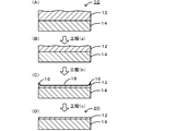
- FIG. Explanatory drawing of the manufacturing method of the composite substrate 20.
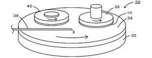
- FIG. The perspective view of the grinding
- FIG. The perspective view of the grinding
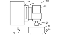
- FIG. Explanatory drawing of the small diameter tool CMP grinder 50.
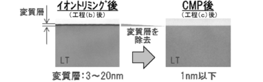
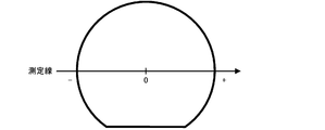
- FIG. Sectional TEM photographs before and after step (c) in Example 1. Explanatory drawing which shows the measurement line of a piezoelectric substrate.
- FIG. 1 is a perspective view of a bonded substrate 10 used in the present embodiment.
- FIG. 2 is an explanatory diagram of a method for manufacturing the composite substrate 20 of the present embodiment.
- FIG. 3 is a perspective view of a polishing portion of a general CMP polishing machine 30 used in the step (a), for example.
- FIG. 4 is a perspective view of a polishing portion of a small diameter tool CMP polishing machine 50 used in, for example, the step (c), and
- FIG. 5 is an explanatory view of the small diameter tool CMP polishing machine 50.
- Step (a) In the step (a), a bonded substrate 10 having a diameter of 2 inches or more obtained by bonding the piezoelectric substrate 12 and the support substrate 14 is used (FIG. 2A).
- the material of the piezoelectric substrate 12 include lithium tantalate, lithium niobate, lithium niobate-lithium tantalate solid solution single crystal, lithium borate, langasite, and quartz.
- the material of the support substrate 14 is silicon, sapphire, aluminum nitride, alumina, alkali-free glass, borosilicate glass, quartz glass, lithium tantalate, lithium niobate, lithium niobate-lithium tantalate solid solution single crystal, lithium borate , Langasite, crystal and the like.
- the piezoelectric substrate 12 may have a diameter of 2 inches or more, preferably 4 inches or more, more preferably 4 to 8 inches, and a thickness of 100 to 1000 ⁇ m, preferably 150 to 500 ⁇ m.
- the support substrate 14 may have the same diameter as the piezoelectric substrate 12 and a thickness of 100 to 1000 ⁇ m, preferably 150 to 500 ⁇ m.
- the bonded substrate 10 may have an orientation flat (OF) as shown in FIG. 1, but may not have an OF.
- the bonded substrate 10 may be a substrate in which the piezoelectric substrate 12 and the support substrate 14 are bonded through an organic adhesive layer, or may be integrated by direct bonding.
- the material for the organic adhesive layer include an epoxy resin and an acrylic resin.
- Direct bonding may be performed by activating the respective bonding surfaces of the piezoelectric substrate and the support substrate and then pressing the two substrates in a state where the bonding surfaces face each other.
- the method for activating the bonding surface include irradiation of an ion beam of an inert gas (such as argon) to the bonding surface, irradiation of plasma or a neutral atom beam, and the like.
- the piezoelectric substrate 12 side of the bonded substrate 10 having a diameter of 2 inches or more where the piezoelectric substrate 12 and the support substrate 14 are bonded is mirror-polished until the thickness of the piezoelectric substrate 12 becomes 20 ⁇ m or less (FIG. 2).
- the reason why the thickness of the piezoelectric substrate 12 is set to 20 ⁇ m or less is to realize good filter characteristics (for example, improvement of temperature characteristics).
- the thickness is preferably 0.1 ⁇ m or more and 20 ⁇ m or less, more preferably 0.5 ⁇ m or more and 15 ⁇ m or less, and further preferably 0.5 ⁇ m or more and 5 ⁇ m or less.
- the lower limit value of the thickness may be set according to the accuracy of machining and the suppression of deterioration of the filter characteristics due to bulk wave reflection at the bonding interface.
- a thickness of 0.1 ⁇ m or more is preferable because relatively high thickness accuracy can be realized and deterioration of filter characteristics due to bulk wave reflection can be suppressed.
- a thickness of 0.5 ⁇ m or more is more preferable because sufficient thickness accuracy can be realized and deterioration of filter characteristics due to bulk wave reflection can be sufficiently suppressed.
- the piezoelectric substrate 12 side of the bonded substrate 10 is first polished with a grinder processing machine, then polished with a lapping machine, and the thickness of the piezoelectric substrate 12 is reduced to 20 ⁇ m or less with a CMP polishing machine.
- Mirror polishing may be used. In this way, the thickness of the piezoelectric substrate 12 can be efficiently reduced to 20 ⁇ m or less.
- CMP is an abbreviation for chemical mechanical polishing.
- a general CMP polishing machine 30 as shown in FIG. 3 may be used as the CMP polishing machine.
- the CMP polishing machine 30 includes a disk-shaped polishing surface plate 32 having a polishing pad 34 and a large diameter, a substrate carrier 36 having a disk shape and a small diameter, and a pipe 38 for supplying slurry containing polishing abrasive grains to the polishing pad 34. And a conditioner 40 for conditioning the polishing pad 34.
- the polishing surface plate 32 includes a shaft and a drive motor (not shown) at the center of the lower surface, and rotates (rotates) when the shaft is rotationally driven by the drive motor.
- Each of the substrate carrier 36 and the conditioner 40 includes a shaft at the center of the upper surface, and rotates (rotates) when the shaft is rotationally driven by a drive motor (not shown).
- the substrate carrier 36 is disposed at a position shifted from the center of the polishing surface plate 32.
- the bonded substrate 10 is mounted on the lower surface of the substrate carrier 36 with the piezoelectric substrate 12 facing downward, and the polishing pad 34 and the substrate carrier 36 of the polishing surface plate 32 are attached.
- the laminated substrate 10 is sandwiched between them. Then, a slurry containing abrasive grains is supplied from the pipe 38 to the polishing pad 34.
- the slurry is supplied between the bonded substrate 10 and the polishing pad 24 of the polishing surface plate 32.
- CMP polishing is performed by rotating the polishing surface plate 32 and the substrate carrier 36 while pressing the bonded substrate 10 against the polishing pad 34 by the substrate carrier 36.
- Step (b) In the step (b), the thickness of the outer peripheral portion 16 of the piezoelectric substrate 12 is thicker than the inner peripheral portion (range inside the outer peripheral portion 16), and the difference between the maximum value and the minimum value of the inner peripheral portion of the piezoelectric substrate 12 is The surface of the piezoelectric substrate 12 is subjected to ion beam processing so as to be 100 nm or less in all planes (FIG. 2C).
- the thickness of the outer peripheral portion 16 of the piezoelectric substrate 12 is larger than that of the inner peripheral portion when the center O of the piezoelectric substrate 12 (when the piezoelectric substrate 12 is a circle, the center of the circle is assumed;
- the outer peripheral portion 16 is thicker than the inner peripheral portion.
- the range of 60 to 100% (preferably 80 to 100%) of the outer diameter of the piezoelectric substrate 12 is defined as the outer peripheral portion 16, and the inner range is defined as the inner peripheral portion. It is good also as saying that thickness becomes thicker than any part of an inner peripheral part.
- a range of 20 mm from the outermost periphery of the piezoelectric substrate 12 is defined as the outer peripheral portion 16, and a range inside thereof is the inner peripheral portion, and the entire range of the outer peripheral portion 16 on the measurement line. It is good also as saying that thickness becomes thicker than any part of an inner peripheral part.
- the difference between the maximum value and the minimum value of the thickness of the inner peripheral portion of the piezoelectric substrate 12 may be 100 nm or less in all planes, but is preferably 50 nm or less, and more preferably 20 nm or less.
- the average thickness (or median) of the outer peripheral portion 16 is preferably 10 to 50 nm thicker than the average (or median) thickness of the inner peripheral portion.
- the thickness increases toward the outermost periphery in the range of 90 to 100% of the outer diameter of the piezoelectric substrate 12 (or within 5 mm from the outermost periphery). Further, it is more preferable that the thickness is increased toward the outermost periphery in the range of 80 to 100% of the outer diameter (or within 10 mm from the outermost periphery), and 60 to 100% of the outer diameter (or from the outermost periphery). More preferably, the thickness is increased toward the outermost periphery within a range of 20 mm or less.
- the rate of increase in thickness in each of the above ranges may be, for example, from 0.5 nm / mm to 10 nm / mm, preferably from 1 nm / mm to 5 nm / mm, and more preferably from 2 nm / mm to 4 nm / mm. Thickness increases toward the outermost circumference, when the thickness increases at a constant rate of increase, or when the thickness increases while the rate of increase changes, for example, the rate of increase tends to be higher or lower toward the outermost circumference.
- the increase rate of the thickness may include an average value of the increasing rate.
- the outer peripheral portion 16 may be processed so that the thickness thereof is the same as the outermost peripheral thickness.
- the outermost peripheral thickness of the piezoelectric substrate 12 may be processed to be 20 nm or more, preferably 30 nm or more, more preferably 40 nm or more than the thinnest portion.
- thickness distribution data of the mirror-polished piezoelectric substrate 12 prior to ion beam processing may be created, and ion beam processing may be performed based on the thickness distribution data of the mirror-polished piezoelectric substrate 12.
- the data of the thickness distribution of the mirror-polished piezoelectric substrate 12 may be created by measuring the thickness of the mirror-polished piezoelectric substrate 12 with an optical film thickness measuring device using laser interference. In this way, thickness distribution data can be created with high accuracy.
- the thickness difference distribution data is created using the thickness distribution data of the mirror-polished piezoelectric substrate 12 and the thickness distribution data of the piezoelectric substrate 12 desired after the ion beam processing.
- the ion beam processing may be performed based on the distribution data.
- the thickness distribution data of the mirror-polished piezoelectric substrate 12 or the above-described thickness difference distribution data is input to an ion beam processing apparatus to determine the beam irradiation time at each point on the surface of the piezoelectric substrate 12.
- processing may be performed using the beam irradiation time. In this way, processing can be performed with high accuracy.
- the beam output value may be constant, and the beam irradiation time may be increased as the thickness difference increases.
- step (b) the thickness distribution data of the mirror-polished piezoelectric substrate 12 or the above-described thickness difference distribution data is input to an ion beam processing apparatus, and the beam output at each point on the surface of the piezoelectric substrate 12 is output. Processing may be performed by determining a value and using the output value of the beam. Even in this case, processing can be performed with high accuracy. In this case, the beam irradiation time is constant, and the beam output value may be increased as the above-described thickness difference increases.
- ion beam processing is preferably performed using an ion beam processing machine equipped with a DC excitation type Ar beam source.
- an ion beam processing machine equipped with a plasma excitation type Ar beam source may be used, but the surface of the piezoelectric substrate 12 is better when an ion beam processing machine equipped with a DC excitation type Ar beam source is used. This is preferable because the deteriorated layer 18 generated in the step is further reduced.
- the bonded substrate 10 obtained in the step (b) has, for example, a thickness of the piezoelectric substrate 12 of 20 ⁇ m or less, and the difference between the maximum value and the minimum value of the thickness is 100 nm or less on all planes including the outer peripheral portion 16. It is good also as what shows the crystallinity whose half width of the obtained rocking curve is 100 arcsec or less.
- Such a bonded substrate 10 is provided with a piezoelectric single crystal thin film (piezoelectric substrate 12) having a high crystallinity and having an arbitrary crystal axis and having a uniform thickness.
- the bonded substrate 10 is applied to an elastic wave device or the like. It can be suitably used.
- Step (c) In the step (c), a polishing pad having a diameter of 5 mm or more and 30 mm or less is used, the polishing pad is rotated while keeping the pressing force by the polishing pad constant, and is moved relative to the piezoelectric substrate 12 to be polished to perform CMP. Polishing is performed to remove at least part of the altered layer 18 generated by the ion beam processing, and the entire surface of the piezoelectric substrate 12 is flattened (the difference in thickness between the outer peripheral portion 16 and the inner peripheral portion is reduced) (FIG. 2). (D)).
- the dwell time at the outer peripheral portion 16 (when the outer peripheral portion 16 has the center of the polishing pad) tends to be shorter than the inner peripheral portion, so that the dwell time becomes relatively shorter with respect to the piezoelectric substrate 12. It may be moved.
- stress tends to concentrate at the time of contact with the polishing pad, and the polishing amount per unit time is larger than that of the inner peripheral portion. Therefore, it is sufficient that the residence time of the polishing pad in the thick outer peripheral portion is short. Can be polished. Further, since the dwell time of the polishing pad at the outer peripheral portion 16 is shorter than that at the inner peripheral portion, sagging due to CMP polishing is less likely to occur.
- the polishing pad may be moved relative to the piezoelectric substrate 12 so that the residence time becomes shorter as the piezoelectric substrate 12 is thinner. In this way, the thickness of the piezoelectric substrate 12 can be made more uniform.
- the residence time of the polishing pad on the outer peripheral portion 16 tends to be shorter than that of the inner peripheral portion, and the residence time tends to be shorter as the piezoelectric substrate 12 is thinner on the inner peripheral portion. You may move relatively with respect to.
- the polishing pad may be moved relative to the piezoelectric substrate 12 so that the residence time is shorter than the residence time corresponding to the thickness. In this way, the thickness of the piezoelectric substrate 12 can be made more uniform, and the occurrence of sagging due to CMP polishing can be further suppressed.
- the thickness distribution data of the piezoelectric substrate 12 processed by the ion beam processing is created prior to the removal of the deteriorated layer 18 and the polishing pad stays on the basis of the data of the thickness distribution of the piezoelectric substrate 12 processed by the ion beam processing.
- the time may be changed.
- the thickness distribution data of the ion beam processed piezoelectric substrate 12 may be created by measuring the thickness of the ion beam processed piezoelectric substrate 12 with a film thickness measuring instrument such as an optical film thickness measuring instrument using laser interference. Good.
- step (c) data on the thickness distribution of the ion beam processed piezoelectric substrate 12 is input to a CMP polishing apparatus to determine the residence time of the polishing pad in each part of the surface of the piezoelectric substrate 12, and the residence time CMP polishing may be performed using
- the residence time may be determined as follows, for example.
- the thickness distribution of the ion beam processed piezoelectric substrate 12 is measured using a film thickness measuring device such as an optical film thickness measuring device, and the thickness Zn at the (Xn, Yn) coordinates of the piezoelectric substrate 12 is determined as (Xn, Yn).
- Zn) data (n is a natural number).
- F (Xn, Yn) K ⁇ f / Zn (Expression (1)).
- K and ⁇ are coefficients
- f is a reference moving speed, and these may be values obtained empirically.
- a small diameter tool CMP polishing machine 50 as shown in FIGS. 4 and 5 may be used as a device used for CMP polishing.
- the small-diameter tool CMP polishing machine 50 includes a disk-shaped and small-diameter head 56 provided with a polishing pad 54, a disk-shaped and large-diameter stage 52, and a pipe 58 that supplies slurry containing abrasive grains to the polishing pad 54. It has.
- the stage 52 includes a drive unit (not shown) and moves in a horizontal plane (X-axis and Y-axis directions).
- the head 56 has a shaft at the center of the upper surface, and rotates (rotates) when the shaft is rotationally driven by a drive motor (not shown).
- the shaft of the head 56 is attached to a support body 60 fixed to a driving unit 62 that moves in the vertical direction via a fixing unit (not shown), and moves in the vertical direction (Z-axis direction).
- the driving unit 62, the driving unit of the stage 52, the driving unit of the head 56, and the like are connected to a control unit (not shown).
- the polishing pad 54 is rotated while the pressing force by the polishing pad 54 is kept constant, and the polishing target 54 It is controlled to move relative to a certain piezoelectric substrate 12.
- the bonded substrate 10 is mounted on the upper surface of the stage 52 with the piezoelectric substrate 12 side facing upward, and bonded between the stage 52 and the polishing pad 54.
- the substrate 10 is sandwiched.
- a slurry containing abrasive grains is supplied from the pipe 58 to the polishing pad 54.
- the slurry is supplied between the bonded substrate 10 and the polishing pad 54.
- the polishing pad 54 is moved relative to the piezoelectric substrate 12 by moving the stage 52 in the horizontal direction, and the pressing force by the polishing pad 54 is kept constant by controlling the vertical movement of the driving unit 62.
- the polishing pad 54 is rotated and the CMP of the bonded substrate 10 is performed.
- the polishing pad 54 and the piezoelectric substrate 12 may be moved relative to each other such that the center of the polishing pad 54 zigzags on the piezoelectric substrate 12 (refer to the path P in FIG. 4), or a spiral You may make it move to a shape.
- a pressing force applied to the polishing pad 54 is measured by a load measuring unit 70 (load cell, dynamometer, etc.) disposed between the support 60 and the drive unit 62, The measured value is input to the control unit described above.
- the control unit controls the vertical movement of the drive unit 62 based on the input measurement value.
- the pressing force by the polishing pad 54 can be kept constant.
- the polishing pad 54 moves relative to the piezoelectric substrate 12 by the movement of the piezoelectric substrate 12.
- the polishing pad 54 moves to the piezoelectric substrate 12 by the movement of the polishing pad 54. It is good also as what moves relatively.
- the piezoelectric substrate 12 may be moved in the vertical direction.
- the thickness of the piezoelectric substrate 12 is 20 ⁇ m or less, preferably 0.1 ⁇ m or more and 10 ⁇ m or less, and the difference between the maximum value and the minimum value is 100 nm or less, preferably 50 nm or less in all planes including the outer peripheral portion 16. More preferably, CMP polishing may be performed so that the thickness is 10 nm or more and 20 nm or less. In the step (c), CMP polishing may be performed so that the thickness of the altered layer 18 is 3 nm or less, preferably 2 nm or less, more preferably 1 nm or less.
- the warp of the obtained composite substrate 20 is preferably 100 ⁇ m or less, more preferably 50 ⁇ m or less, and further preferably 10 ⁇ m or less.
- a composite substrate having fewer altered layers 18 can be provided.
- the small-diameter tool CMP polishing is performed on the bonded substrate 10 that has been subjected to the ion beam processing so that the thickness of the outer peripheral portion 16 of the piezoelectric substrate 12 is increased under appropriate conditions, sagging due to the small-diameter tool CMP polishing is less likely to occur. .
- thickness distribution of the piezoelectric substrate 12 is more suitable. Can be.
- the composite substrate obtained by the method for manufacturing a composite substrate of the present invention can be used as an acoustic wave device by forming an electrode pattern on the surface of a piezoelectric substrate, for example.
- the present invention is not limited to the above-described embodiment, and it goes without saying that the present invention can be implemented in various modes as long as it belongs to the technical scope of the present invention.
- the surface of the piezoelectric substrate 12 is processed using an ion beam, but is processed using a neutral atom beam (for example, an Ar neutral atom beam) instead of the ion beam. May be. Even if it does in this way, the effect similar to embodiment mentioned above is acquired.
- Example 1 A silicon substrate (support substrate) and a LiNbO 3 substrate (piezoelectric substrate) having a thickness of 230 ⁇ m and a diameter of 2 inches polished on both sides were prepared. These substrates were introduced into a vacuum chamber maintaining a degree of vacuum on the order of 10 ⁇ 6 Pa, and the bonded surfaces were held facing each other. The bonded surfaces of both substrates were irradiated with Ar beam for 80 seconds, and the inactive layer on the surface was removed and activated. Next, the substrates were brought into contact with each other and bonded with a load of 1200 kgf. After taking out the bonded substrate thus obtained, the piezoelectric substrate side was ground by a grinder processing machine until the thickness became 10 ⁇ m.
- the bonded substrate was set on a lapping machine and polished with a diamond slurry until the thickness of the piezoelectric substrate became 3 ⁇ m. Further, the surface of the piezoelectric substrate was mirror-polished with a CMP grinder until the thickness became 0.8 ⁇ m. At this time, colloidal silica was used as an abrasive. (Process (a))
- the thickness of the piezoelectric substrate was measured with an optical film thickness measuring instrument using laser interference, the thickness was within a range of ⁇ 0.1 ⁇ m in the entire plane including the outer peripheral portion of the piezoelectric substrate centered on 0.8 ⁇ m. It was. The total number of measurement points was 80 on all planes except for the chamfered end of the piezoelectric substrate.
- the bonded substrate thus obtained was set in an ion beam processing machine equipped with a plasma excitation type Ar beam source.
- the data of the thickness distribution of the mirror-polished piezoelectric substrate measured by the optical film thickness measuring instrument and the thickness distribution data desired after ion beam processing are ionized.
- the thickness difference distribution data was created by importing into a beam processing machine, and the processing amount at each measurement point of the piezoelectric substrate, here the Ar beam irradiation time, was determined using the thickness difference distribution data.
- the irradiation time of the beam was adjusted by the feeding speed of the bonded substrate.
- the center film thickness was 450 nm, and the difference between the maximum value and the minimum value was 65 nm on the entire plane including the outer periphery.
- the rocking curve was measured with an X-ray diffractometer, the half-value width (FWHM) was 80 arcsec, a value equivalent to that of a bulk single crystal.
- the bonded substrate thus obtained was set in a small-diameter tool CMP polishing machine 50 shown in FIGS.
- the thickness distribution data of the ion beam processed piezoelectric substrate measured by the optical film thickness measuring instrument described above is imported into the small-diameter tool CMP polishing machine 50, and the dwell time of the polishing pad 54 is calculated by the above-described formula (1).
- the small diameter tool CMP grinder 50 was operated using this residence time, and small diameter tool CMP grinding
- a composite substrate of Example 1 was obtained.
- FIG. 6 shows cross-sectional TEM photographs before and after the step (c).
- an altered layer was observed on the surface.
- the thickness of the altered layer was 5 nm.
- no altered layer was observed after step (c).
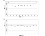
- FIG. 8 shows the thickness distribution of the piezoelectric substrate before and after step (c) in Example 1.
- FIG. 8A shows the thickness distribution before step (c)
- FIG. 8B shows the thickness distribution after step (c).
- Example 1 no sagging of the outer peripheral portion was confirmed after step (c), as shown in FIG. 8 (B).
- the warpage (SORI) of the composite substrate of Example 1 was measured in accordance with SEMI (Semiconductor Equipment and Materials International) standards.
- SEMI semiconductor Equipment and Materials International
- a FlatMaster manufactured by Corning Tropel was used.
- the warpage of the composite substrate of Example 1 was 5 ⁇ m.
- Example 2 A silicon substrate (support substrate) and a LiNbO 3 substrate (piezoelectric substrate) having a thickness of 230 ⁇ m and a diameter of 2 inches polished on both sides were prepared. These substrates were introduced into a vacuum chamber maintaining a degree of vacuum on the order of 10 ⁇ 6 Pa, and the bonded surfaces were held facing each other. The bonded surfaces of both substrates were irradiated with Ar beam for 80 seconds, and the inactive layer on the surface was removed and activated. Next, the substrates were brought into contact with each other and bonded under a load of 1200 kgf. After taking out the bonded substrate thus obtained, the piezoelectric substrate side was ground by a grinder processing machine until the thickness became 10 ⁇ m.
- the bonded substrate was set on a lapping machine and polished with diamond slurry until the thickness of the piezoelectric substrate reached 5 ⁇ m. Further, the surface of the piezoelectric substrate was mirror-polished with a CMP grinder until the thickness became 2.5 ⁇ m. At this time, colloidal silica was used as an abrasive. (Process (a))
- the thickness of the piezoelectric substrate was measured with an optical film thickness measuring instrument using laser interference, the thickness was within the range of ⁇ 0.1 ⁇ m in the entire plane including the outer periphery of the piezoelectric substrate with 2.5 ⁇ m as the center. It was. The total number of measurement points was 80 on all planes except for the chamfered end of the piezoelectric substrate.
- the bonded substrate thus obtained was set in an ion beam processing machine equipped with a plasma excitation type Ar beam source.
- the data of the thickness distribution of the mirror-polished piezoelectric substrate measured by the optical film thickness measuring instrument and the thickness distribution data desired after ion beam processing are ionized.
- the thickness difference distribution data was created by importing into a beam processing machine, and the processing amount at each measurement point of the piezoelectric substrate, here the Ar beam irradiation time, was determined using the thickness difference distribution data.
- the irradiation time of the beam was adjusted by the feeding speed of the bonded substrate.
- the center film thickness was 1910 nm, and the difference between the maximum value and the minimum value was 40 nm on the entire plane including the outer periphery.
- the rocking curve was measured with an X-ray diffractometer, the half-value width (FWHM) was 80 arcsec, a value equivalent to that of a bulk single crystal.
- the bonded substrate thus obtained was set in a small-diameter tool CMP polishing machine 50 shown in FIGS.
- the thickness distribution data of the ion beam processed piezoelectric substrate measured by the optical film thickness measuring instrument described above is imported into the small-diameter tool CMP polishing machine 50, and the dwell time of the polishing pad 54 is calculated by the above-described formula (1).
- the small diameter tool CMP grinder 50 was operated using this residence time, and small diameter tool CMP grinding
- a composite substrate of Example 2 was obtained.
- FIG. 9 shows the thickness distribution of the piezoelectric substrate before and after step (c) in Example 1.
- FIG. 9A shows the thickness distribution before step (c)
- FIG. 9B shows the thickness distribution after step (c).
- Example 2 no sagging of the outer peripheral portion was confirmed after the step (c) as shown in FIG. 9B.
- Example 3 A silicon substrate (support substrate) and a LiNbO 3 substrate (piezoelectric substrate) having a thickness of 230 ⁇ m and a diameter of 2 inches polished on both sides were prepared. These substrates were introduced into a vacuum chamber maintaining a degree of vacuum on the order of 10 ⁇ 6 Pa, and the bonded surfaces were held facing each other. The bonded surfaces of both substrates were irradiated with Ar beam for 80 seconds, and the inactive layer on the surface was removed and activated. Next, the substrates were brought into contact with each other and bonded under a load of 1200 kgf. After taking out the bonded substrate thus obtained, the piezoelectric substrate side was ground by a grinder processing machine until the thickness became 10 ⁇ m.
- the bonded substrate was set on a lapping machine and polished with a diamond slurry until the thickness of the piezoelectric substrate reached 4 ⁇ m. Further, the surface of the piezoelectric substrate was mirror-polished with a CMP grinder until the thickness became 1.8 ⁇ m. At this time, colloidal silica was used as an abrasive. (Process (a))
- the thickness of the piezoelectric substrate was measured with an optical film thickness measuring instrument using laser interference, the thickness was within the range of ⁇ 0.1 ⁇ m in all planes including the outer periphery of the piezoelectric substrate centered at 1.8 ⁇ m. It was. The total number of measurement points was 80 on all planes except for the chamfered end of the piezoelectric substrate.
- the bonded substrate thus obtained was set in an ion beam processing machine equipped with a plasma excitation type Ar beam source.
- the data of the thickness distribution of the mirror-polished piezoelectric substrate measured by the optical film thickness measuring instrument and the thickness distribution data desired after ion beam processing are ionized.
- the thickness difference distribution data was created by importing into a beam processing machine, and the processing amount at each measurement point of the piezoelectric substrate, here the Ar beam irradiation time, was determined using the thickness difference distribution data.
- the irradiation time of the beam was adjusted by the feeding speed of the bonded substrate.
- the center film thickness was 1185 nm, and the difference between the maximum value and the minimum value was 95 nm in all planes including the outer peripheral portion.
- the rocking curve was measured with an X-ray diffractometer, the half-value width (FWHM) was 80 arcsec, a value equivalent to that of a bulk single crystal.
- the bonded substrate thus obtained was set in a small-diameter tool CMP polishing machine 50 shown in FIGS.
- the thickness distribution data of the ion beam processed piezoelectric substrate measured by the optical film thickness measuring instrument described above is imported into the small-diameter tool CMP polishing machine 50, and the dwell time of the polishing pad 54 is calculated by the above-described formula (1).
- the small diameter tool CMP grinder 50 was operated using this residence time, and small diameter tool CMP grinding
- a composite substrate of Example 3 was obtained.
- FIG. 10 shows the thickness distribution of the piezoelectric substrate before and after step (c) in Example 1.
- 10A shows the thickness distribution before step (c)
- FIG. 10B shows the thickness distribution after step (c).
- Example 3 the sagging of the outer peripheral portion was not confirmed after the step (c) as shown in FIG.
- Comparative Example 1 A composite substrate of Comparative Example 1 was obtained in the same manner as in Example 1 except that in the step (b), ion beam processing was performed so that the outer peripheral portion and the inner peripheral portion had the same thickness.
- the central film thickness was 450 nm, and the difference between the maximum value and the minimum value was 100 nm on the entire plane including the outer peripheral portion.
- the rocking curve was measured with an X-ray diffractometer, the half-value width (FWHM) was 80 arcsec, a value equivalent to that of a bulk single crystal.
- FIG. 11 shows the thickness distribution of the piezoelectric substrate before and after step (c) in Comparative Example 1.
- FIG. 11A shows the thickness distribution before step (c)
- FIG. 11B shows the thickness distribution after step (c).
- Comparative Example 1 even after the step (c), as shown in FIG. 11 (B), sagging occurred in the outer peripheral portion, and the outermost peripheral thickness was reduced by 100 nm or more.
- the present invention can be used for an acoustic wave device such as a SAW filter.
Landscapes
- Engineering & Computer Science (AREA)
- Manufacturing & Machinery (AREA)
- Mechanical Engineering (AREA)
- Physics & Mathematics (AREA)
- Acoustics & Sound (AREA)
- Geometry (AREA)
- Microelectronics & Electronic Packaging (AREA)
- Finish Polishing, Edge Sharpening, And Grinding By Specific Grinding Devices (AREA)
- Mechanical Treatment Of Semiconductor (AREA)
- Welding Or Cutting Using Electron Beams (AREA)
- Surface Acoustic Wave Elements And Circuit Networks Thereof (AREA)
Abstract
Description
(a)圧電基板と支持基板とを接合した直径2インチ以上の貼り合わせ基板の圧電基板側を、前記圧電基板の厚みが20μm以下になるまで鏡面研磨する工程と、
(b)前記圧電基板の外周部の厚みが内周部よりも厚くかつ前記圧電基板の内周部の厚みの最大値と最小値の差が全平面で100nm以下となるようにイオンビーム又は中性原子ビームを用いて加工する工程と、
(c)直径5mm以上30mm以下の研磨パッドを用い、前記研磨パッドによる押圧力を一定に保ちながら前記研磨パッドを回転させるとともに前記圧電基板に対して相対的に移動させてCMP研磨を行い、前記工程(b)でイオンビーム又は中性原子ビームを用いて加工したことによって生じた変質層の少なくとも一部を除去し、前記圧電基板の全面を平らにする工程と、
を含む。
工程(a)では、圧電基板12と支持基板14とを接合した直径2インチ以上の貼り合わせ基板10を用いる(図2(A))。圧電基板12の材質としては、タンタル酸リチウム、ニオブ酸リチウム、ニオブ酸リチウム-タンタル酸リチウム固溶体単結晶、硼酸リチウム、ランガサイト、水晶などが挙げられる。支持基板14の材質としては、シリコン、サファイア、窒化アルミニウム、アルミナ、無アルカリガラス、ホウ珪酸ガラス、石英ガラス、タンタル酸リチウム、ニオブ酸リチウム、ニオブ酸リチウム-タンタル酸リチウム固溶体単結晶、ホウ酸リチウム、ランガサイト、水晶などが挙げられる。圧電基板12の大きさは、直径2インチ以上、好ましくは4インチ以上、より好ましくは4~8インチであり、厚さが100~1000μm、好ましくは150~500μmであるものとしてもよい。支持基板14の大きさは、直径が圧電基板12と同じであり、厚さが100~1000μm、好ましくは150~500μmであるものとしてもよい。なお、貼り合わせ基板10は、図1に示すようにオリエンテーションフラット(OF)を有してもよいが、OFを有さなくてもよい。
工程(b)では、圧電基板12の外周部16の厚みが内周部(外周部16より内側の範囲)よりも厚くかつ圧電基板12の内周部の厚みの最大値と最小値の差が全平面で100nm以下となるように圧電基板12の表面をイオンビーム加工する(図2(C))。
工程(c)では、直径5mm以上30mm以下の研磨パッドを用い、研磨パッドによる押圧力を一定に保ちながら研磨パッドを回転させるとともに研磨対象である圧電基板12に対して相対的に移動させてCMP研磨を行い、前記イオンビーム加工によって生じた変質層18の少なくとも一部を除去し、圧電基板12の全面を平らに(外周部16と内周部との厚みの差を小さく)する(図2(D))。
両面研磨された厚みが230μm、直径が2インチのシリコン基板(支持基板)、LiNbO3基板(圧電基板)をそれぞれ用意した。これら基板を10-6Pa台の真空度を保つ真空チャンバーに導入し、接合面を対向させ保持した。両基板の接合面にArビームを80sec間照射し、表面の不活性層を除去し活性化した。次いで互いの基板を接触させ、1200kgfの荷重をかけて接合した。このようにして得られた貼り合わせ基板を取り出した後、グラインダー加工機により圧電基板側をその厚みが10μmになるまで研削した。ついで、その貼り合わせ基板をラップ加工機にセットし、ダイヤモンドスラリーを用いて圧電基板の厚みが3μmになるまで研磨した。更に、その圧電基板の表面をCMP研磨機で厚みが0.8μmになるまで鏡面研磨した。この時、研磨剤としてコロイダルシリカを用いた。(工程(a))
両面研磨された厚みが230μm、直径が2インチのシリコン基板(支持基板)、LiNbO3基板(圧電基板)をそれぞれ用意した。これら基板を10-6Pa台の真空度を保つ真空チャンバーに導入し、接合面を対向させ保持した。両基板の接合面にArビームを80sec間照射し、表面の不活性層を除去し活性化した。ついで互いの基板を接触させ、1200kgfの荷重をかけて接合した。このようにして得られた貼り合わせ基板を取り出した後、グラインダー加工機により圧電基板側をその厚みが10μmになるまで研削した。ついで、その貼り合わせ基板をラップ加工機にセットし、ダイヤモンドスラリーを用いて圧電基板の厚みが5μmになるまで研磨した。更に、その圧電基板の表面をCMP研磨機で厚みが2.5μmになるまで鏡面研磨した。この時、研磨剤としてコロイダルシリカを用いた。(工程(a))
両面研磨された厚みが230μm、直径が2インチのシリコン基板(支持基板)、LiNbO3基板(圧電基板)をそれぞれ用意した。これら基板を10-6Pa台の真空度を保つ真空チャンバーに導入し、接合面を対向させ保持した。両基板の接合面にArビームを80sec間照射し、表面の不活性層を除去し活性化した。ついで互いの基板を接触させ、1200kgfの荷重をかけて接合した。このようにして得られた貼り合わせ基板を取り出した後、グラインダー加工機により圧電基板側をその厚みが10μmになるまで研削した。ついで、その貼り合わせ基板をラップ加工機にセットし、ダイヤモンドスラリーを用いて圧電基板の厚みが4μmになるまで研磨した。更に、その圧電基板の表面をCMP研磨機で厚みが1.8μmになるまで鏡面研磨した。この時、研磨剤としてコロイダルシリカを用いた。(工程(a))
工程(b)において、外周部の厚みと内周部の厚みとが同程度になるようにイオンビーム加工を行った以外は、実施例1と同様に比較例1の複合基板を得た。
Claims (8)
- (a)圧電基板と支持基板とを接合した直径2インチ以上の貼り合わせ基板の圧電基板側を、前記圧電基板の厚みが20μm以下になるまで鏡面研磨する工程と、
(b)前記圧電基板の外周部の厚みが内周部よりも厚くかつ前記圧電基板の内周部の厚みの最大値と最小値の差が全平面で100nm以下となるようにイオンビーム又は中性原子ビームを用いて加工する工程と、
(c)直径5mm以上30mm以下の研磨パッドを用い、前記研磨パッドによる押圧力を一定に保ちながら前記研磨パッドを回転させるとともに前記圧電基板に対して相対的に移動させてCMP研磨を行い、前記工程(b)でイオンビーム又は中性原子ビームを用いて加工したことによって生じた変質層の少なくとも一部を除去し、前記圧電基板の全面を平らにする工程と、
を含む複合基板の製造方法。 - 前記工程(c)では、前記研磨パッドを、外周部での滞留時間が内周部よりも短くなる傾向で前記圧電基板に対して相対的に移動させる、請求項1に記載の複合基板の製造方法。
- 前記工程(c)では、前記研磨パッドを、前記圧電基板が薄いほど滞留時間が短くなる傾向で前記圧電基板に対して相対的に移動させる、請求項1に記載の複合基板の製造方法。
- 前記工程(c)では、前記研磨パッドを、外周部での滞留時間が内周部よりも短くなる傾向でかつ内周部では前記圧電基板が薄いほど滞留時間が短くなる傾向で前記圧電基板に対して相対的に移動させる、請求項1に記載の複合基板の製造方法。
- 前記工程(b)では、前記圧電基板の外周部の厚みの平均値が内周部の厚みの平均値に比べて10~50nm厚くなるようにイオンビーム又は中性原子ビームを用いて加工する、請求項1~4のいずれか1項に記載の複合基板の製造方法。
- 前記工程(b)では、前記圧電基板の外径の90~100%又は最外周から5mm以内の範囲において最外周に向けて厚みが増加するようにイオンビーム又は中性原子ビームを用いて加工する、請求項1~5のいずれか1項に記載の複合基板の製造方法。
- 前記工程(b)では、前記範囲における厚みの増加率が0.5nm/mm以上10nm/mm以下となるようにイオンビーム又は中性原子ビームを用いて加工する、請求項6に記載の複合基板の製造方法。
- 前記工程(b)では、前記圧電基板の最外周の厚みが、厚みの最も薄い部分よりも20nm以上厚くなるようにイオンビーム又は中性原子ビームを用いて加工する、請求項1~7のいずれか1項に記載の複合基板の製造方法。
Priority Applications (5)
| Application Number | Priority Date | Filing Date | Title |
|---|---|---|---|
| CN201680002597.0A CN108028312B (zh) | 2015-09-15 | 2016-09-14 | 复合基板的制造方法 |
| DE112016000126.6T DE112016000126B4 (de) | 2015-09-15 | 2016-09-14 | Herstellungsverfahren für Verbundwerkstoff-Substrat |
| KR1020177006433A KR101794488B1 (ko) | 2015-09-15 | 2016-09-14 | 복합 기판의 제조 방법 |
| JP2016574205A JP6100984B1 (ja) | 2015-09-15 | 2016-09-14 | 複合基板の製造方法 |
| US15/449,053 US9935257B2 (en) | 2015-09-15 | 2017-03-03 | Production method for composite substrate |
Applications Claiming Priority (2)
| Application Number | Priority Date | Filing Date | Title |
|---|---|---|---|
| JP2015181762 | 2015-09-15 | ||
| JP2015-181762 | 2015-09-15 |
Related Child Applications (1)
| Application Number | Title | Priority Date | Filing Date |
|---|---|---|---|
| US15/449,053 Continuation US9935257B2 (en) | 2015-09-15 | 2017-03-03 | Production method for composite substrate |
Publications (1)
| Publication Number | Publication Date |
|---|---|
| WO2017047604A1 true WO2017047604A1 (ja) | 2017-03-23 |
Family
ID=58288833
Family Applications (1)
| Application Number | Title | Priority Date | Filing Date |
|---|---|---|---|
| PCT/JP2016/077032 Ceased WO2017047604A1 (ja) | 2015-09-15 | 2016-09-14 | 複合基板の製造方法 |
Country Status (7)
| Country | Link |
|---|---|
| US (1) | US9935257B2 (ja) |
| JP (1) | JP6100984B1 (ja) |
| KR (1) | KR101794488B1 (ja) |
| CN (1) | CN108028312B (ja) |
| DE (1) | DE112016000126B4 (ja) |
| TW (1) | TWI599445B (ja) |
| WO (1) | WO2017047604A1 (ja) |
Cited By (7)
| Publication number | Priority date | Publication date | Assignee | Title |
|---|---|---|---|---|
| JP6393015B1 (ja) * | 2017-05-02 | 2018-09-19 | 日本碍子株式会社 | 弾性波素子およびその製造方法 |
| WO2018203430A1 (ja) * | 2017-05-02 | 2018-11-08 | 日本碍子株式会社 | 弾性波素子およびその製造方法 |
| JP2019029941A (ja) * | 2017-08-02 | 2019-02-21 | 株式会社ディスコ | 弾性波デバイス用基板の製造方法 |
| WO2019039475A1 (ja) * | 2017-08-25 | 2019-02-28 | 日本碍子株式会社 | 接合体および弾性波素子 |
| WO2019039474A1 (ja) * | 2017-08-25 | 2019-02-28 | 日本碍子株式会社 | 接合体および弾性波素子 |
| WO2019220721A1 (ja) * | 2018-05-16 | 2019-11-21 | 日本碍子株式会社 | 圧電性材料基板と支持基板との接合体 |
| JP2021074804A (ja) * | 2019-11-06 | 2021-05-20 | 株式会社ディスコ | 加工装置 |
Families Citing this family (6)
| Publication number | Priority date | Publication date | Assignee | Title |
|---|---|---|---|---|
| TWD174921S (zh) * | 2014-12-17 | 2016-04-11 | 日本碍子股份有限公司 | 複合基板之部分 |
| CN109273586A (zh) * | 2018-08-17 | 2019-01-25 | 福建晶安光电有限公司 | 一种压电晶片及其制作方法 |
| CN111092148B (zh) * | 2019-12-27 | 2022-08-09 | 厦门市三安集成电路有限公司 | 一种压电材料复合基板的制造方法 |
| CN111740008B (zh) * | 2020-06-17 | 2022-07-22 | 上海新硅聚合半导体有限公司 | 一种提高离子束剥离薄膜厚度均匀性的方法 |
| CN115582736A (zh) * | 2022-10-10 | 2023-01-10 | 北京创思工贸有限公司 | 单晶硅平面楔形光学零件的抛光方法 |
| CN117140345A (zh) * | 2023-09-14 | 2023-12-01 | 浙江美迪凯光学半导体有限公司 | 一种射频芯片铌酸锂衬底SiO2层平坦化的工艺 |
Citations (5)
| Publication number | Priority date | Publication date | Assignee | Title |
|---|---|---|---|---|
| JP2001118812A (ja) * | 1999-08-09 | 2001-04-27 | Nikon Corp | 化学機械研磨装置および半導体デバイス製造方法 |
| JP2001308049A (ja) * | 2000-04-19 | 2001-11-02 | Okamoto Machine Tool Works Ltd | 基板加工における加工手段の移動速度の補正方法 |
| WO2014104098A1 (ja) * | 2012-12-26 | 2014-07-03 | 日本碍子株式会社 | 複合基板、その製法及び弾性波デバイス |
| WO2014156507A1 (ja) * | 2013-03-27 | 2014-10-02 | 日本碍子株式会社 | 複合基板及び弾性波デバイス |
| JP2015145054A (ja) * | 2014-02-04 | 2015-08-13 | 日本碍子株式会社 | 複合基板の研磨方法及び複合基板 |
Family Cites Families (15)
| Publication number | Priority date | Publication date | Assignee | Title |
|---|---|---|---|---|
| US20030168169A1 (en) | 2000-08-03 | 2003-09-11 | Akira Ishikawa | Chemical-mechanical polishing apparatus, polishing pad and method for manufacturing semiconductor device |
| US7314402B2 (en) | 2001-11-15 | 2008-01-01 | Speedfam-Ipec Corporation | Method and apparatus for controlling slurry distribution |
| DE102004045181B4 (de) * | 2004-09-17 | 2016-02-04 | Epcos Ag | SAW-Bauelement mit reduziertem Temperaturgang und Verfahren zur Herstellung |
| JP4870377B2 (ja) * | 2005-03-31 | 2012-02-08 | 京セラキンセキ株式会社 | 水晶部品のべべリング加工方法 |
| US20070257580A1 (en) * | 2006-05-05 | 2007-11-08 | Fujifilm Dimatix, Inc. | Polishing Piezoelectric Material |
| CN101689841A (zh) | 2007-12-25 | 2010-03-31 | 株式会社村田制作所 | 复合压电基板的制造方法 |
| JP5317092B2 (ja) * | 2008-03-23 | 2013-10-16 | Hoya株式会社 | マスクブランク用基板の製造方法、多層反射膜付き基板の製造方法、及び反射型マスクブランクの製造方法、並びに反射型マスクの製造方法 |
| JP5276035B2 (ja) * | 2009-04-13 | 2013-08-28 | 日本電波工業株式会社 | 圧電デバイスの製造方法及び圧電デバイス |
| CN102474239B (zh) * | 2009-07-30 | 2014-10-29 | 日本碍子株式会社 | 复合基板及其制造方法 |
| KR101443015B1 (ko) | 2012-08-17 | 2014-09-22 | 엔지케이 인슐레이터 엘티디 | 복합 기판, 탄성 표면파 디바이스 및 복합 기판의 제조방법 |
| KR101497888B1 (ko) * | 2012-11-14 | 2015-03-02 | 엔지케이 인슐레이터 엘티디 | 복합 기판 및 그 제법 |
| KR101511001B1 (ko) * | 2012-11-14 | 2015-04-10 | 엔지케이 인슐레이터 엘티디 | 복합 기판 |
| JP5934424B2 (ja) * | 2013-02-19 | 2016-06-15 | 日本碍子株式会社 | 弾性波デバイスの製法 |
| KR20150121029A (ko) * | 2013-02-19 | 2015-10-28 | 가부시키가이샤 리프 | Cmp 장치 및 cmp 방법 |
| WO2015012005A1 (ja) * | 2013-07-25 | 2015-01-29 | 日本碍子株式会社 | 複合基板及びその製法 |
-
2016
- 2016-09-14 CN CN201680002597.0A patent/CN108028312B/zh active Active
- 2016-09-14 DE DE112016000126.6T patent/DE112016000126B4/de active Active
- 2016-09-14 WO PCT/JP2016/077032 patent/WO2017047604A1/ja not_active Ceased
- 2016-09-14 KR KR1020177006433A patent/KR101794488B1/ko active Active
- 2016-09-14 TW TW105129944A patent/TWI599445B/zh active
- 2016-09-14 JP JP2016574205A patent/JP6100984B1/ja active Active
-
2017
- 2017-03-03 US US15/449,053 patent/US9935257B2/en active Active
Patent Citations (5)
| Publication number | Priority date | Publication date | Assignee | Title |
|---|---|---|---|---|
| JP2001118812A (ja) * | 1999-08-09 | 2001-04-27 | Nikon Corp | 化学機械研磨装置および半導体デバイス製造方法 |
| JP2001308049A (ja) * | 2000-04-19 | 2001-11-02 | Okamoto Machine Tool Works Ltd | 基板加工における加工手段の移動速度の補正方法 |
| WO2014104098A1 (ja) * | 2012-12-26 | 2014-07-03 | 日本碍子株式会社 | 複合基板、その製法及び弾性波デバイス |
| WO2014156507A1 (ja) * | 2013-03-27 | 2014-10-02 | 日本碍子株式会社 | 複合基板及び弾性波デバイス |
| JP2015145054A (ja) * | 2014-02-04 | 2015-08-13 | 日本碍子株式会社 | 複合基板の研磨方法及び複合基板 |
Cited By (22)
| Publication number | Priority date | Publication date | Assignee | Title |
|---|---|---|---|---|
| JP6393015B1 (ja) * | 2017-05-02 | 2018-09-19 | 日本碍子株式会社 | 弾性波素子およびその製造方法 |
| WO2018203430A1 (ja) * | 2017-05-02 | 2018-11-08 | 日本碍子株式会社 | 弾性波素子およびその製造方法 |
| TWI780103B (zh) * | 2017-05-02 | 2022-10-11 | 日商日本碍子股份有限公司 | 彈性波元件及其製造方法 |
| US10879871B2 (en) | 2017-05-02 | 2020-12-29 | Ngk Insulators, Ltd. | Elastic wave element and method for manufacturing same |
| JP2019029941A (ja) * | 2017-08-02 | 2019-02-21 | 株式会社ディスコ | 弾性波デバイス用基板の製造方法 |
| CN110945787A (zh) * | 2017-08-25 | 2020-03-31 | 日本碍子株式会社 | 接合体以及弹性波元件 |
| CN110945786B (zh) * | 2017-08-25 | 2021-02-19 | 日本碍子株式会社 | 接合体及弹性波元件 |
| JPWO2019039474A1 (ja) * | 2017-08-25 | 2019-11-07 | 日本碍子株式会社 | 接合体および弾性波素子 |
| CN110945787B (zh) * | 2017-08-25 | 2023-06-02 | 日本碍子株式会社 | 接合体以及弹性波元件 |
| US11637541B2 (en) | 2017-08-25 | 2023-04-25 | Ngk Insulators, Ltd. | Joined body and elastic wave element |
| JP6507326B1 (ja) * | 2017-08-25 | 2019-04-24 | 日本碍子株式会社 | 接合体および弾性波素子 |
| CN110945786A (zh) * | 2017-08-25 | 2020-03-31 | 日本碍子株式会社 | 接合体及弹性波元件 |
| TWI699015B (zh) * | 2017-08-25 | 2020-07-11 | 日商日本碍子股份有限公司 | 接合體及彈性波元件 |
| WO2019039474A1 (ja) * | 2017-08-25 | 2019-02-28 | 日本碍子株式会社 | 接合体および弾性波素子 |
| JP2019140697A (ja) * | 2017-08-25 | 2019-08-22 | 日本碍子株式会社 | 接合体および弾性波素子 |
| US10931256B2 (en) | 2017-08-25 | 2021-02-23 | Ngk Insulators, Ltd. | Joined body and elastic wave element |
| WO2019039475A1 (ja) * | 2017-08-25 | 2019-02-28 | 日本碍子株式会社 | 接合体および弾性波素子 |
| US11082025B2 (en) | 2018-05-16 | 2021-08-03 | Ngk Insulators, Ltd. | Joined body of piezoelectric material substrate and support substrate |
| JP6648346B1 (ja) * | 2018-05-16 | 2020-02-14 | 日本碍子株式会社 | 圧電性材料基板と支持基板との接合体 |
| WO2019220721A1 (ja) * | 2018-05-16 | 2019-11-21 | 日本碍子株式会社 | 圧電性材料基板と支持基板との接合体 |
| JP2021074804A (ja) * | 2019-11-06 | 2021-05-20 | 株式会社ディスコ | 加工装置 |
| JP7378894B2 (ja) | 2019-11-06 | 2023-11-14 | 株式会社ディスコ | 加工装置 |
Also Published As
| Publication number | Publication date |
|---|---|
| CN108028312A (zh) | 2018-05-11 |
| TWI599445B (zh) | 2017-09-21 |
| JP6100984B1 (ja) | 2017-03-22 |
| US20170179371A1 (en) | 2017-06-22 |
| KR20170078593A (ko) | 2017-07-07 |
| TW201722622A (zh) | 2017-07-01 |
| JPWO2017047604A1 (ja) | 2017-09-14 |
| DE112016000126T5 (de) | 2017-06-01 |
| DE112016000126B4 (de) | 2020-06-25 |
| US9935257B2 (en) | 2018-04-03 |
| KR101794488B1 (ko) | 2017-11-06 |
| CN108028312B (zh) | 2021-03-26 |
Similar Documents
| Publication | Publication Date | Title |
|---|---|---|
| JP6100984B1 (ja) | 複合基板の製造方法 | |
| JP6265915B2 (ja) | 複合基板の製法 | |
| CN108352442B (zh) | 复合基板及压电基板的厚度趋势推定方法 | |
| TWI761547B (zh) | 彈性波器件用基板的製造方法 | |
| JP7271875B2 (ja) | 酸化物単結晶基板の製造方法 | |
| US7588481B2 (en) | Wafer polishing method and polished wafer | |
| JP6226774B2 (ja) | 複合基板の製法及び複合基板 | |
| JPH10256203A (ja) | 鏡面仕上げされた薄板状ウェーハの製造方法 | |
| JP5871282B2 (ja) | 圧電性酸化物単結晶ウェーハの製造方法。 | |
| JP6097896B1 (ja) | 複合基板及び圧電基板の厚み傾向推定方法 | |
| JP2007260793A (ja) | ウェーハ基板の研磨方法及び圧電性単結晶からなるウェーハ | |
| Li et al. | Hybrid polishing of fused silica glass with bound-abrasive polishers in conjunction with vibration | |
| US20260025117A1 (en) | Method for manufacturing bonded body | |
| JP2010023166A (ja) | 単結晶基板の製造方法 |
Legal Events
| Date | Code | Title | Description |
|---|---|---|---|
| ENP | Entry into the national phase |
Ref document number: 2016574205 Country of ref document: JP Kind code of ref document: A |
|
| ENP | Entry into the national phase |
Ref document number: 20177006433 Country of ref document: KR Kind code of ref document: A |
|
| WWE | Wipo information: entry into national phase |
Ref document number: 112016000126 Country of ref document: DE |
|
| 121 | Ep: the epo has been informed by wipo that ep was designated in this application |
Ref document number: 16846475 Country of ref document: EP Kind code of ref document: A1 |
|
| 122 | Ep: pct application non-entry in european phase |
Ref document number: 16846475 Country of ref document: EP Kind code of ref document: A1 |