WO2017047272A1 - 半導体記憶装置および半導体記憶装置におけるデータ消去方法 - Google Patents
半導体記憶装置および半導体記憶装置におけるデータ消去方法 Download PDFInfo
- Publication number
- WO2017047272A1 WO2017047272A1 PCT/JP2016/072919 JP2016072919W WO2017047272A1 WO 2017047272 A1 WO2017047272 A1 WO 2017047272A1 JP 2016072919 W JP2016072919 W JP 2016072919W WO 2017047272 A1 WO2017047272 A1 WO 2017047272A1
- Authority
- WO
- WIPO (PCT)
- Prior art keywords
- page
- data
- pages
- erasing
- state
- Prior art date
- Legal status (The legal status is an assumption and is not a legal conclusion. Google has not performed a legal analysis and makes no representation as to the accuracy of the status listed.)
- Ceased
Links
Images


Classifications
-
- G—PHYSICS
- G11—INFORMATION STORAGE
- G11C—STATIC STORES
- G11C16/00—Erasable programmable read-only memories
- G11C16/02—Erasable programmable read-only memories electrically programmable
- G11C16/06—Auxiliary circuits, e.g. for writing into memory
- G11C16/10—Programming or data input circuits
- G11C16/14—Circuits for erasing electrically, e.g. erase voltage switching circuits
- G11C16/16—Circuits for erasing electrically, e.g. erase voltage switching circuits for erasing blocks, e.g. arrays, words, groups
-
- G—PHYSICS
- G06—COMPUTING OR CALCULATING; COUNTING
- G06F—ELECTRIC DIGITAL DATA PROCESSING
- G06F12/00—Accessing, addressing or allocating within memory systems or architectures
- G06F12/02—Addressing or allocation; Relocation
- G06F12/0223—User address space allocation, e.g. contiguous or non contiguous base addressing
- G06F12/023—Free address space management
- G06F12/0238—Memory management in non-volatile memory, e.g. resistive RAM or ferroelectric memory
- G06F12/0246—Memory management in non-volatile memory, e.g. resistive RAM or ferroelectric memory in block erasable memory, e.g. flash memory
-
- G—PHYSICS
- G06—COMPUTING OR CALCULATING; COUNTING
- G06F—ELECTRIC DIGITAL DATA PROCESSING
- G06F3/00—Input arrangements for transferring data to be processed into a form capable of being handled by the computer; Output arrangements for transferring data from processing unit to output unit, e.g. interface arrangements
- G06F3/06—Digital input from, or digital output to, record carriers, e.g. RAID, emulated record carriers or networked record carriers
- G06F3/0601—Interfaces specially adapted for storage systems
- G06F3/0602—Interfaces specially adapted for storage systems specifically adapted to achieve a particular effect
- G06F3/0608—Saving storage space on storage systems
-
- G—PHYSICS
- G06—COMPUTING OR CALCULATING; COUNTING
- G06F—ELECTRIC DIGITAL DATA PROCESSING
- G06F3/00—Input arrangements for transferring data to be processed into a form capable of being handled by the computer; Output arrangements for transferring data from processing unit to output unit, e.g. interface arrangements
- G06F3/06—Digital input from, or digital output to, record carriers, e.g. RAID, emulated record carriers or networked record carriers
- G06F3/0601—Interfaces specially adapted for storage systems
- G06F3/0628—Interfaces specially adapted for storage systems making use of a particular technique
- G06F3/0646—Horizontal data movement in storage systems, i.e. moving data in between storage devices or systems
- G06F3/0652—Erasing, e.g. deleting, data cleaning, moving of data to a wastebasket
-
- G—PHYSICS
- G06—COMPUTING OR CALCULATING; COUNTING
- G06F—ELECTRIC DIGITAL DATA PROCESSING
- G06F3/00—Input arrangements for transferring data to be processed into a form capable of being handled by the computer; Output arrangements for transferring data from processing unit to output unit, e.g. interface arrangements
- G06F3/06—Digital input from, or digital output to, record carriers, e.g. RAID, emulated record carriers or networked record carriers
- G06F3/0601—Interfaces specially adapted for storage systems
- G06F3/0668—Interfaces specially adapted for storage systems adopting a particular infrastructure
- G06F3/0671—In-line storage system
- G06F3/0673—Single storage device
- G06F3/0679—Non-volatile semiconductor memory device, e.g. flash memory, one time programmable memory [OTP]
-
- G—PHYSICS
- G06—COMPUTING OR CALCULATING; COUNTING
- G06F—ELECTRIC DIGITAL DATA PROCESSING
- G06F3/00—Input arrangements for transferring data to be processed into a form capable of being handled by the computer; Output arrangements for transferring data from processing unit to output unit, e.g. interface arrangements
- G06F3/06—Digital input from, or digital output to, record carriers, e.g. RAID, emulated record carriers or networked record carriers
- G06F3/08—Digital input from, or digital output to, record carriers, e.g. RAID, emulated record carriers or networked record carriers from or to individual record carriers, e.g. punched card, memory card, integrated circuit [IC] card or smart card
-
- G—PHYSICS
- G11—INFORMATION STORAGE
- G11C—STATIC STORES
- G11C11/00—Digital stores characterised by the use of particular electric or magnetic storage elements; Storage elements therefor
- G11C11/56—Digital stores characterised by the use of particular electric or magnetic storage elements; Storage elements therefor using storage elements with more than two stable states represented by steps, e.g. of voltage, current, phase, frequency
- G11C11/5621—Digital stores characterised by the use of particular electric or magnetic storage elements; Storage elements therefor using storage elements with more than two stable states represented by steps, e.g. of voltage, current, phase, frequency using charge storage in a floating gate
- G11C11/5628—Programming or writing circuits; Data input circuits
-
- G—PHYSICS
- G11—INFORMATION STORAGE
- G11C—STATIC STORES
- G11C16/00—Erasable programmable read-only memories
- G11C16/02—Erasable programmable read-only memories electrically programmable
- G11C16/06—Auxiliary circuits, e.g. for writing into memory
- G11C16/26—Sensing or reading circuits; Data output circuits
-
- G—PHYSICS
- G06—COMPUTING OR CALCULATING; COUNTING
- G06F—ELECTRIC DIGITAL DATA PROCESSING
- G06F2212/00—Indexing scheme relating to accessing, addressing or allocation within memory systems or architectures
- G06F2212/72—Details relating to flash memory management
- G06F2212/7205—Cleaning, compaction, garbage collection, erase control
-
- G—PHYSICS
- G11—INFORMATION STORAGE
- G11C—STATIC STORES
- G11C16/00—Erasable programmable read-only memories
- G11C16/02—Erasable programmable read-only memories electrically programmable
- G11C16/04—Erasable programmable read-only memories electrically programmable using variable threshold transistors, e.g. FAMOS
- G11C16/0483—Erasable programmable read-only memories electrically programmable using variable threshold transistors, e.g. FAMOS comprising cells having several storage transistors connected in series
Definitions
- the present disclosure relates to a semiconductor memory device and a data erasing method in the semiconductor memory device.
- a non-volatile semiconductor memory such as a NAND flash memory has a plurality of blocks each composed of a plurality of pages. Data writing and reading are collectively performed in units of pages, but data erasure is generally performed in units of blocks.
- Japanese Patent Application Laid-Open No. 2004-228561 proposes a technique for increasing the speed when deleting only the data of some pages in a block, but there is a possibility that a useless area may be generated in the block. In addition, there is a possibility that data of pages other than those to be erased cannot be read correctly.
- a semiconductor memory device includes a block having a plurality of pages and a controller that controls writing, erasing, and reading of data, and each page has four or more states.
- the controller has a plurality of memory cells that can change to any one of the states, and the controller erases only a part of the plurality of pages. The predetermined data that only occurs in one stage is overwritten.
- a data erasing method in a semiconductor memory device includes a block having a plurality of pages, and each page can be in any one of four or more states.
- predetermined data that causes only one stage of state change is generated in some pages. It is intended to be overwritten.
- the semiconductor memory device or the data erasing method in the semiconductor memory device when only some of the plurality of pages are erased, Since predetermined data that changes only in one stage is overwritten, the data of some pages in the block can be erased safely and at high speed. Note that the effects described here are not necessarily limited, and may be any of the effects described in the present disclosure.
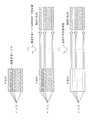
- FIG. 10 is an explanatory diagram showing an example of changes in the state of memory cells and data when only page A is erased in MLC.
- MLC after erasing only page B, after erasing only page A, it is explanatory drawing which shows an example of the change of the state and data of a memory cell.
- MLC it is explanatory drawing which shows an example of the change of the state of a memory cell, and data in the case of erasing only page B after erasing only page A.
- TLC it is explanatory drawing which shows an example of the change of the state of a memory cell in the case of erasing only page A, and data.
- TLC it is explanatory drawing which shows an example of the change of the state of a memory cell in the case of erasing only page B, and data.
- TLC it is explanatory drawing which shows an example of the change of the state and data of a memory cell in the case of erasing only page C.
- FIG. 1 shows an example of a writing unit and an erasing unit of a general nonvolatile semiconductor memory as a comparative example.
- FIG. 2 shows an operation example at the time of erasing data in a general nonvolatile semiconductor memory as a comparative example.
- a non-volatile semiconductor memory such as a NAND flash memory includes a plurality of blocks 1 each composed of a plurality of pages 2 as shown in FIG.
- Memory cells for storing data are arranged at the intersections of word lines and bit lines. One or more pages of data are stored on one word line. Data writing and reading are performed collectively in units of two pages. Data is erased collectively in units of one block. Thus, data writing and reading and data erasing are performed in different units. For this reason, normally, it is not possible to erase only the data of some pages 4 in the block 1 as shown in the upper part of FIG.
- Patent Document 1 Japanese Patent Laid-Open No. 2014-96122 proposes two types of methods. One is that writing only one file in one block eliminates the need to save data during erasure. In this method, there is a problem that when a small file is written, there is a lot of wasted area in the block. The other is a method of destroying data on the page to be erased by overwriting the data on the page to be erased. Writing in a nonvolatile semiconductor memory that requires an erasing operation makes a transition only in the direction in which the cell potential increases. Therefore, if data is overwritten on a written page, there is a possibility that neither the written data nor the overwritten data can be read.
- FIG. 3 shows an example of the coupling phenomenon in the nonvolatile semiconductor memory.
- Patent Document 1 proposes random data or data with the highest cell potential as data to be overwritten.
- a NAND flash memory has a phenomenon called coupling that is affected by peripheral memory cells.
- this is a phenomenon in which the cell potential appears to change at the time of reading when a potential difference between a certain memory cell and a peripheral adjacent memory cell is large.
- the read potential appears to be higher than the original potential.
- the potential of the memory cell of the overwritten page becomes high, and the cell potential of the page on the peripheral word line, particularly the page on the front and back word lines may appear high. . If the cell potential looks high, written data may not be read correctly, which may lead to unintended data destruction.
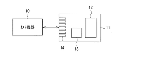
- FIG. 4 shows an example of the semiconductor memory device 11 according to an embodiment of the present disclosure.
- the semiconductor memory device 11 includes a nonvolatile semiconductor memory 12, a controller 13, and a host I / F (interface) 14.
- Nonvolatile semiconductor memory 12 is, for example, a NAND flash memory.
- the non-volatile semiconductor memory 12 includes a plurality of blocks 1 composed of a plurality of pages 2 in substantially the same manner as the comparative example shown in FIG.
- the operation of the nonvolatile semiconductor memory 12 is controlled by the controller 13.
- the host I / F 14 is an interface for connecting the controller 13 and a host device 10 such as a PC (personal computer).
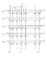
- the nonvolatile semiconductor memory 12 has a matrix configuration in which the word lines (WL) 21 and the bit lines (BL) 22 intersect as shown in FIG.
- the intersection of WL21 and BL22 is a memory cell 23 for storing data.
- the selection line 24 determines the voltage of the BL 22 in order to determine a value to be written in each memory cell 23 at the time of writing.
- One or more pages of data are stored on one word line 21.
- the memory cell 23 has, for example, an MLC (Multi Level Cell) or TLC (Triple Level Cell) configuration.
- MLC Multi Level Cell
- TLC Triple Level Cell
- data for 2 bits can be stored in one memory cell 23, and data for 2 pages can be stored in one WL21.
- TLC data for 3 bits can be stored in one memory cell 23, and data for 3 pages can be stored in one WL21.
- the write data is transmitted to the controller 13 via the host I / F 14.
- the controller 13 writes the data scrambled by the output of the linear feedback shift register (LFSR) or the like in the nonvolatile semiconductor memory 12 in order to suppress the influence of the coupling with the adjacent memory cell 23.
- the writing position is determined by the controller 13, and information on the writing position called a logical-physical conversion table is held.
- the host device 10 When the host device 10 reads data from the nonvolatile semiconductor memory 12, the read address is notified to the controller 13 via the host I / F 14.
- the controller 13 obtains the position where the data is written using the logical-physical conversion table, reads the data from the nonvolatile semiconductor memory 12, releases the scramble, and transmits the data to the host via the host I / F 14. .
- the controller 13 When the host device 10 erases data from the nonvolatile semiconductor memory 12, the controller 13 is notified of the erase address via the host I / F 14. The controller 13 uses the logical / physical conversion table to obtain the position where the data is written. Note that if the data in the logical-physical conversion table is rewritten, data in the nonvolatile semiconductor memory 12 cannot normally be read from the host device 10. However, even in that case, since data remains in the nonvolatile semiconductor memory 12, the data may be read by connecting a measuring instrument to the terminal of the nonvolatile semiconductor memory 12. For this reason, to securely erase data, it is necessary to erase page 2 in which data is written. When the controller 13 confirms that no valid data remains on another page 2 in the same block 1, the controller 13 erases the block 1. If valid data remains, page 2 in which data to be deleted is written is overwritten with predetermined data to be described later, and the logical-physical conversion table at the corresponding address is also deleted.
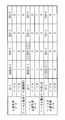
- FIG. 9 shows an example of the relationship between the cell potential of the MLC, the state, and the data of each page A and B.
- data for 2 bits can be stored in one memory cell 23, and data for 2 pages can be stored in one WL21.
- page A the first page on one WL 21
- page B the second page
- Page B is higher than Page A.
- one memory cell 23 can take four stages of an erase state, an A state, a B state, and a C state.
- the higher cell potential is called the upper state
- the lower cell potential is called the lower state.
- the lowest state is the erase state, and the highest state is the C state.
- the threshold voltage between the erase state and the A state is A
- the threshold voltage between the A state and the B state is B
- the threshold voltage between the B state and the C state is C.
- Predetermined data that changes only in one stage is created and overwritten.
- predetermined data is created and overwritten so that the state change occurs only in one stage from lower to higher. Since data to be written is usually scrambled, it is assumed that the number of memory cells 23 at each voltage level is not greatly different between a block unit and a page unit.
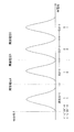
- FIG. 6 shows an example of changes in the state and data of the memory cell 23 when only page A is erased in the MLC.
- the controller 13 reads written data in a plurality of pages including a part of pages 4 to be erased, and generates predetermined data to be overwritten on the page A based on the read data. Specifically, when erasing page A, the controller 13 reads the data of page A and the data of page B, calculates the logical product of the data of the corresponding bits, and generates predetermined data. The predetermined data is overwritten on page A.
- the state of each memory cell 23 changes as shown in FIG. 6 by writing. As shown in FIG. 6, the data of page B is retained even after predetermined data is overwritten on page A.
- FIG. 7 shows an example of changes in the state and data of the memory cell 23 when only page A is erased after erasing only page B in the MLC.
- controller 13 stores “1” as predetermined data for all memory cells 23 in page B. Overwrite the data.
- the state of each memory cell 23 changes as shown in FIG. 7 by writing.
- the data of the page A is retained even after the predetermined data is overwritten on the page B.
- about 1/4 bits are inverted from 0 to 1, so that correct data cannot be acquired. Thereby, the data of page B is substantially erased.
- each memory cell 23 in page B changes only to the next higher state even if the state changes. For this reason, the influence on the data written on the other pages 2 of the preceding and succeeding WLs 21 can be suppressed with respect to the WL21 in which some pages 4 to be erased exist.
- Predetermined data is generated by calculating the logical product of the data.
- the predetermined data is overwritten on page A.
- the state of each memory cell 23 changes as shown in FIG. 7 by writing.
- the data of page B is retained even after predetermined data is overwritten on page A.
- about 1/4 of the bits are inverted from 1 to 0, so that correct data cannot be acquired. Thereby, the data of page A is substantially erased.
- FIG. 8 shows an example of changes in the state and data of the memory cell 23 when only page B is erased after erasing only page A in the MLC.
- controller 13 overwrites data “0” as predetermined data in all memory cells 23 in page B. .
- the state of each memory cell 23 changes as shown in FIG. 8 by writing. Compared to before the page A is erased, only the memory cell 23 in the erase state and the A state changes to the next higher state, and about 1/4 of the bits in both the page A and the page B are inverted from 1 to 0. Therefore, correct data cannot be acquired.
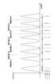
- FIG. 10 shows an example of the relationship between the cell potential of TLC, the state, and the data of each page A, B, C.
- data for 3 bits can be stored in one memory cell 23, and data for 3 pages can be stored in one WL21.
- the first page on one WL 21 is page A
- the second page is page B
- the third page is page C.
- page B is higher than page A
- page C is higher than page B.
- one memory cell 23 can take eight states of an erase state, an A state, a B state, a C state, a D state, an E state, an F state, and a G state.
- the higher cell potential is called the upper state
- the lower cell potential is called the lower state.
- the lowest state is the erase state
- the highest state is the G state.
- the threshold voltage between the erase state and the A state is A
- the threshold voltage between the A state and the B state is B
- the threshold voltage between the B state and the C state is C.
- the threshold voltage between the C state and the D state is D
- the threshold voltage between the D state and the E state is E
- the threshold voltage between the E state and the F state is F
- the threshold voltage between the F state and the G state is G.
- predetermined data that changes only in one stage and overwrite it.
- predetermined data is generated or selected so that the state change occurs only in one stage from the lower level to the higher level and is overwritten.
- page A or page Data “1” is overwritten as predetermined data in all the memory cells 23 in B.
- page C is erased as a part of pages 4 to be erased
- data “0” is overwritten as predetermined data in all memory cells 23 in page C.
- the state of the memory cell 23 changes as shown in FIGS. 11 to 13 by writing.
- FIG. 11 shows an example of changes in the state and data of the memory cell 23 when only page A is erased in TLC.
- FIG. 12 shows an example of changes in the state and data of the memory cell 23 when only page B is erased in TLC.
- FIG. 13 shows an example of changes in the state and data of the memory cell 23 when only page C is erased in TLC.
- a data pattern of predetermined data is determined based on the current page state and data state, and the predetermined data is overwritten on a part of pages 4 to be erased.
- the present technology can take the following configurations.
- (1) A block having a plurality of pages; And a controller for controlling writing, erasing and reading of data,
- Each page includes a plurality of memory cells, each of which can change to any one of four or more states.
- the controller when erasing only a part of the plurality of pages, overwrites the part of the page with predetermined data such that the state change occurs only in one stage.
- Semiconductor memory device .
- the semiconductor memory device according to (1) above.
- the semiconductor memory device reads written data in a plurality of pages including the partial page, and generates the predetermined data based on the read data .
- the semiconductor memory device wherein data of a logical product with the second page is overwritten.
- the plurality of pages includes a first page and a second page, The controller is When erasing the second page as the partial page before erasing the first page, the predetermined data is used as the predetermined data for all the memory cells in the second page.
- the plurality of pages includes a first page and a second page, The controller is When erasing the first page as the partial page, the first page and the second page are used as the predetermined data for all the memory cells in the first page. Overwrite the logical product with the page, Thereafter, when erasing the second page as the partial page, data “0” is set as the predetermined data for all the memory cells in the second page.
- the semiconductor memory device according to (2) which is overwritten.
- the semiconductor memory device can change to a four-stage state.
- the plurality of pages on the one word line include first to third pages, The controller is When erasing the first page or the second page as the partial page, all the memory cells in the first page or all the memory cells in the second page On the other hand, “1” data is overwritten as the predetermined data, When erasing the third page as the partial page, data “0” is overwritten as the predetermined data in all the memory cells in the third page.
- the semiconductor memory device according to (2).
- the semiconductor memory device (9) The semiconductor memory device according to (8), wherein the memory cell can change to eight states.
- a semiconductor memory device comprising a block having a plurality of pages, and each page having a plurality of memory cells each of which can be in any one of four or more stages.
- a method of erasing data in a semiconductor memory device wherein only a part of the plurality of pages is erased by overwriting predetermined data in which the state change occurs only in one stage. .
Landscapes
- Engineering & Computer Science (AREA)
- Theoretical Computer Science (AREA)
- Physics & Mathematics (AREA)
- General Engineering & Computer Science (AREA)
- General Physics & Mathematics (AREA)
- Human Computer Interaction (AREA)
- Computer Hardware Design (AREA)
- Microelectronics & Electronic Packaging (AREA)
- Read Only Memory (AREA)
Priority Applications (1)
| Application Number | Priority Date | Filing Date | Title |
|---|---|---|---|
| US15/758,021 US10658042B2 (en) | 2015-09-15 | 2016-08-04 | Semiconductor memory device and method of erasing data of partial page and overwriting partial page with predetermined data |
Applications Claiming Priority (2)
| Application Number | Priority Date | Filing Date | Title |
|---|---|---|---|
| JP2015181628A JP2017059281A (ja) | 2015-09-15 | 2015-09-15 | 半導体記憶装置および半導体記憶装置におけるデータ消去方法 |
| JP2015-181628 | 2015-09-15 |
Publications (1)
| Publication Number | Publication Date |
|---|---|
| WO2017047272A1 true WO2017047272A1 (ja) | 2017-03-23 |
Family
ID=58288872
Family Applications (1)
| Application Number | Title | Priority Date | Filing Date |
|---|---|---|---|
| PCT/JP2016/072919 Ceased WO2017047272A1 (ja) | 2015-09-15 | 2016-08-04 | 半導体記憶装置および半導体記憶装置におけるデータ消去方法 |
Country Status (3)
| Country | Link |
|---|---|
| US (1) | US10658042B2 (enExample) |
| JP (1) | JP2017059281A (enExample) |
| WO (1) | WO2017047272A1 (enExample) |
Families Citing this family (2)
| Publication number | Priority date | Publication date | Assignee | Title |
|---|---|---|---|---|
| KR102603916B1 (ko) | 2018-04-25 | 2023-11-21 | 삼성전자주식회사 | 불휘발성 메모리 장치 및 제어기를 포함하는 스토리지 장치 |
| GB2620445B (en) * | 2022-07-08 | 2024-12-04 | Kirintec Ltd | Data erasure system |
Citations (1)
| Publication number | Priority date | Publication date | Assignee | Title |
|---|---|---|---|---|
| JP2014038687A (ja) * | 2012-08-10 | 2014-02-27 | Samsung Electronics Co Ltd | 多様なメモリセル状態定義を有する不揮発性メモリ装置とそのプログラミング方法及び動作方法並びにこれを備えたメモリシステム |
Family Cites Families (4)
| Publication number | Priority date | Publication date | Assignee | Title |
|---|---|---|---|---|
| US7580151B2 (en) * | 2003-10-01 | 2009-08-25 | Seiko Epson Corporation | Image processing system and method, printing system |
| JP2014096122A (ja) | 2012-11-12 | 2014-05-22 | Genusion:Kk | 不揮発性半導体記憶装置を用いた記憶媒体のファイルの記録方法 |
| US9098401B2 (en) * | 2012-11-21 | 2015-08-04 | Apple Inc. | Fast secure erasure schemes for non-volatile memory |
| US20160155495A1 (en) * | 2013-07-08 | 2016-06-02 | Wilus Institute Of Standards And Technology Inc. | Memory system and method for processing data in memory |
-
2015
- 2015-09-15 JP JP2015181628A patent/JP2017059281A/ja not_active Ceased
-
2016
- 2016-08-04 WO PCT/JP2016/072919 patent/WO2017047272A1/ja not_active Ceased
- 2016-08-04 US US15/758,021 patent/US10658042B2/en not_active Expired - Fee Related
Patent Citations (1)
| Publication number | Priority date | Publication date | Assignee | Title |
|---|---|---|---|---|
| JP2014038687A (ja) * | 2012-08-10 | 2014-02-27 | Samsung Electronics Co Ltd | 多様なメモリセル状態定義を有する不揮発性メモリ装置とそのプログラミング方法及び動作方法並びにこれを備えたメモリシステム |
Also Published As
| Publication number | Publication date |
|---|---|
| US20180254088A1 (en) | 2018-09-06 |
| JP2017059281A (ja) | 2017-03-23 |
| US10658042B2 (en) | 2020-05-19 |
Similar Documents
| Publication | Publication Date | Title |
|---|---|---|
| CN101681300B (zh) | 存储器系统 | |
| KR102190694B1 (ko) | 불휘발성 메모리 시스템 및 그것의 동작 방법 | |
| JP5497754B2 (ja) | アドホックフラッシュメモリ基準セル | |
| US9575839B2 (en) | Data storage device and operating method thereof | |
| US20160170671A1 (en) | Data storage device and data writing method thereof | |
| US9940058B2 (en) | Data storage device and data maintenance method thereof | |
| US9520184B2 (en) | Method for writing in-system programming code into flash memory for better noise margin | |
| JP2005108303A (ja) | 不揮発性半導体記憶装置 | |
| US10241678B2 (en) | Data storage device and data writing method capable of avoiding repeated write operation of a TLC block when interrupted | |
| JP2008108418A (ja) | マルチページプログラムの方法、及びこれを行うためのフラッシュメモリ装置 | |
| US20170115933A1 (en) | Data storage device and data maintenance method thereof | |
| US20170285953A1 (en) | Data Storage Device and Data Maintenance Method thereof | |
| JP2005339231A (ja) | メモリカード、半導体装置、及び半導体メモリの制御方法 | |
| KR102785741B1 (ko) | 메모리 장치 및 메모리 장치의 동작방법 | |
| US10902922B2 (en) | Nonvolatile memory device storing data in sub-blocks and operating method thereof | |
| CN107507644A (zh) | 存储器装置及其操作方法 | |
| JP2009158082A (ja) | メモリへのデータ書き込み方法及びデータ読み取り方法 | |
| CN108231119B (zh) | 用每单元分数比特低延迟读取快闪存储设备的方法和装置 | |
| KR100967026B1 (ko) | 불휘발성 메모리 장치 및 그 캐쉬리드 방법 | |
| WO2017047272A1 (ja) | 半導体記憶装置および半導体記憶装置におけるデータ消去方法 | |
| US20160306569A1 (en) | Memory system | |
| CN112435705A (zh) | 存储器系统 | |
| KR100965079B1 (ko) | 불휘발성 메모리 장치 | |
| US9373367B1 (en) | Data storage device and operating method thereof | |
| KR100960478B1 (ko) | 불휘발성 메모리 장치의 듀얼 플레인 카피백 방법 |
Legal Events
| Date | Code | Title | Description |
|---|---|---|---|
| 121 | Ep: the epo has been informed by wipo that ep was designated in this application |
Ref document number: 16846145 Country of ref document: EP Kind code of ref document: A1 |
|
| WWE | Wipo information: entry into national phase |
Ref document number: 15758021 Country of ref document: US |
|
| NENP | Non-entry into the national phase |
Ref country code: DE |
|
| 122 | Ep: pct application non-entry in european phase |
Ref document number: 16846145 Country of ref document: EP Kind code of ref document: A1 |