WO2017043348A1 - 磁気シールド構造 - Google Patents
磁気シールド構造 Download PDFInfo
- Publication number
- WO2017043348A1 WO2017043348A1 PCT/JP2016/075114 JP2016075114W WO2017043348A1 WO 2017043348 A1 WO2017043348 A1 WO 2017043348A1 JP 2016075114 W JP2016075114 W JP 2016075114W WO 2017043348 A1 WO2017043348 A1 WO 2017043348A1
- Authority
- WO
- WIPO (PCT)
- Prior art keywords
- magnetic shield
- shield structure
- case
- shield body
- structure according
- Prior art date
- Legal status (The legal status is an assumption and is not a legal conclusion. Google has not performed a legal analysis and makes no representation as to the accuracy of the status listed.)
- Ceased
Links
Images





Classifications
-
- H—ELECTRICITY
- H01—ELECTRIC ELEMENTS
- H01H—ELECTRIC SWITCHES; RELAYS; SELECTORS; EMERGENCY PROTECTIVE DEVICES
- H01H45/00—Details of relays
- H01H45/10—Electromagnetic or electrostatic shielding
-
- H—ELECTRICITY
- H01—ELECTRIC ELEMENTS
- H01F—MAGNETS; INDUCTANCES; TRANSFORMERS; SELECTION OF MATERIALS FOR THEIR MAGNETIC PROPERTIES
- H01F27/00—Details of transformers or inductances, in general
- H01F27/34—Special means for preventing or reducing unwanted electric or magnetic effects, e.g. no-load losses, reactive currents, harmonics, oscillations, leakage fields
- H01F27/36—Electric or magnetic shields or screens
- H01F27/363—Electric or magnetic shields or screens made of electrically conductive material
-
- H—ELECTRICITY
- H01—ELECTRIC ELEMENTS
- H01F—MAGNETS; INDUCTANCES; TRANSFORMERS; SELECTION OF MATERIALS FOR THEIR MAGNETIC PROPERTIES
- H01F27/00—Details of transformers or inductances, in general
- H01F27/02—Casings
-
- H—ELECTRICITY
- H01—ELECTRIC ELEMENTS
- H01F—MAGNETS; INDUCTANCES; TRANSFORMERS; SELECTION OF MATERIALS FOR THEIR MAGNETIC PROPERTIES
- H01F27/00—Details of transformers or inductances, in general
- H01F27/34—Special means for preventing or reducing unwanted electric or magnetic effects, e.g. no-load losses, reactive currents, harmonics, oscillations, leakage fields
- H01F27/36—Electric or magnetic shields or screens
-
- H—ELECTRICITY
- H01—ELECTRIC ELEMENTS
- H01H—ELECTRIC SWITCHES; RELAYS; SELECTORS; EMERGENCY PROTECTIVE DEVICES
- H01H45/00—Details of relays
- H01H45/02—Bases; Casings; Covers
-
- H—ELECTRICITY
- H01—ELECTRIC ELEMENTS
- H01H—ELECTRIC SWITCHES; RELAYS; SELECTORS; EMERGENCY PROTECTIVE DEVICES
- H01H50/00—Details of electromagnetic relays
- H01H50/10—Electromagnetic or electrostatic shielding
-
- H—ELECTRICITY
- H05—ELECTRIC TECHNIQUES NOT OTHERWISE PROVIDED FOR
- H05K—PRINTED CIRCUITS; CASINGS OR CONSTRUCTIONAL DETAILS OF ELECTRIC APPARATUS; MANUFACTURE OF ASSEMBLAGES OF ELECTRICAL COMPONENTS
- H05K9/00—Screening of apparatus or components against electric or magnetic fields
- H05K9/0007—Casings
-
- H—ELECTRICITY
- H10—SEMICONDUCTOR DEVICES; ELECTRIC SOLID-STATE DEVICES NOT OTHERWISE PROVIDED FOR
- H10W—GENERIC PACKAGES, INTERCONNECTIONS, CONNECTORS OR OTHER CONSTRUCTIONAL DETAILS OF DEVICES COVERED BY CLASS H10
- H10W42/00—Arrangements for protection of devices
- H10W42/20—Arrangements for protection of devices protecting against electromagnetic or particle radiation, e.g. light, X-rays, gamma-rays or electrons
-
- H—ELECTRICITY
- H10—SEMICONDUCTOR DEVICES; ELECTRIC SOLID-STATE DEVICES NOT OTHERWISE PROVIDED FOR
- H10W—GENERIC PACKAGES, INTERCONNECTIONS, CONNECTORS OR OTHER CONSTRUCTIONAL DETAILS OF DEVICES COVERED BY CLASS H10
- H10W44/00—Electrical arrangements for controlling or matching impedance
- H10W44/20—Electrical arrangements for controlling or matching impedance at high-frequency [HF] or radio frequency [RF]
-
- H—ELECTRICITY
- H01—ELECTRIC ELEMENTS
- H01H—ELECTRIC SWITCHES; RELAYS; SELECTORS; EMERGENCY PROTECTIVE DEVICES
- H01H15/00—Switches having rectilinearly-movable operating part or parts adapted for actuation in opposite directions, e.g. slide switch
- H01H15/02—Details
-
- H—ELECTRICITY
- H10—SEMICONDUCTOR DEVICES; ELECTRIC SOLID-STATE DEVICES NOT OTHERWISE PROVIDED FOR
- H10W—GENERIC PACKAGES, INTERCONNECTIONS, CONNECTORS OR OTHER CONSTRUCTIONAL DETAILS OF DEVICES COVERED BY CLASS H10
- H10W44/00—Electrical arrangements for controlling or matching impedance
- H10W44/20—Electrical arrangements for controlling or matching impedance at high-frequency [HF] or radio frequency [RF]
- H10W44/226—Electrical arrangements for controlling or matching impedance at high-frequency [HF] or radio frequency [RF] for HF amplifiers
- H10W44/234—Arrangements for impedance matching
Definitions
- the present invention is a magnetic shield structure, particularly a magnetic shield structure formed by metal plating on the housing.
- the high-frequency relay is configured by covering a relay body configured by covering a body with a metal case. For this reason, the high frequency relay requires a separate metal case, has a large number of parts and assembly steps, and has low productivity.
- the external dimensions of the metal case and the positional relationship between the metal case and the high-frequency transmission component affect the high-frequency characteristics. For this reason, high dimensional accuracy and assembly accuracy are required in the manufacture and assembly of the metal case, and the manufacture and assembly are not easy.
- the metal case covers the entire exposed surface except the installation surface of the relay body. For this reason, there exists a problem that a desired high frequency characteristic cannot be obtained as a result by the said metal case covering the area
- an object of the present invention is to provide a magnetic shield structure that has high productivity, is easy to manufacture and assemble, and has excellent high frequency characteristics.
- a magnetic shield structure according to the present invention is a magnetic shield body formed by metal plating at least one of an outer surface and an inner surface forming a surface of a housing made of a dielectric material. Is provided.
- the magnetic shield body is directly provided on the housing, the number of parts and the number of assembling steps can be reduced, and a highly productive magnetic shield structure can be obtained. Further, the magnetic shield body is directly formed in a necessary area of the housing. For this reason, it is possible to prevent a decrease in high frequency characteristics based on variations in dimensional accuracy and assembly accuracy of the housing. Then, the magnetic shield body is formed only in a necessary region of the housing. For this reason, a magnetic shield body is not formed in a region where the characteristics of the transmission line structure are deteriorated or an unnecessary region unlike the conventional example. As a result, there is an effect that a magnetic shield structure having excellent high frequency characteristics can be obtained.
- FIG. 1 is a perspective view showing an electromagnetic relay of a first embodiment to which a magnetic shield structure according to the present invention is applied. It is a perspective view which shows the state which erase
- FIG. 2 is a perspective view of only the magnetic shield body shown in FIG. 1. It is a graph which shows the analysis result of the Example which concerns on 1st Embodiment, and a comparative example.
- FIG. 10 is a perspective view of only the magnetic shield provided in the case shown in FIG. 9. It is a perspective view of only the magnetic shield body located inside in FIG. It is the perspective view which looked at the case shown in FIG. 9 from a different viewpoint. It is the perspective view which looked at only the shield body shown in FIG. 10 from a different angle.
- FIG. 10 is a partial enlarged cross-sectional view of the case shown in FIG. 9. It is a partial expanded sectional view of only the magnetic shield body of the case shown in FIG. It is a perspective view which shows the switch of 3rd Embodiment to which the magnetic shield structure concerning this invention is applied.
- FIG. 17 is a central front sectional view of the switch shown in FIG. 16. It is a perspective view which shows the state which erase
- FIG. 20 is a perspective view showing a state where the operation lever is deleted from FIG. 19. It is a perspective view which shows the state which erase
- FIG. 17 is a cross-sectional perspective view of only the magnetic shield body shown in FIG. 16. It is a disassembled perspective view which shows the connector of 4th Embodiment to which the magnetic shield structure concerning this invention is applied. It is a cross-sectional exploded perspective view of the connector shown in FIG. It is a perspective view which shows the state which erase
- a magnetic shield body formed by metal plating is provided on at least one of an outer surface and an inner surface forming a surface of a housing made of a dielectric material. .
- the magnetic shield body is directly provided on the housing, the number of parts and the number of assembling steps are reduced, and a highly productive magnetic shield structure can be obtained.
- the magnetic shield body is directly formed in a necessary area of the housing. For this reason, it is possible to prevent a decrease in high frequency characteristics based on variations in dimensional accuracy and assembly accuracy of the housing. Then, the magnetic shield body is formed only in a necessary region of the housing. For this reason, a magnetic shield body is not formed in a region where the characteristics of the transmission line structure are deteriorated or an unnecessary region unlike the conventional example. As a result, there is an effect that a magnetic shield structure having excellent high frequency characteristics can be obtained.
- the characteristic impedance of the high-frequency transmission path is uniform in a region facing the high-frequency transmission path disposed in the housing on the inner surface and / or outer surface of the housing.
- the magnetic shield may be provided by the metal plating. According to this aspect, it is not always necessary to provide a magnetic shield body by metal plating on the entire inner surface and / or outer surface of the housing. For this reason, raw material can be saved and a highly productive magnetic shield structure can be obtained.
- a characteristic impedance of the high-frequency transmission line is present in a region of the inner surface and / or outer surface of the housing facing the high-frequency transmission line disposed in the housing.
- the magnetic shield may be provided with the metal plating and dielectric so as to be uniform. According to this aspect, it is not always necessary to provide a magnetic shield body with metal plating and dielectric on the entire inner surface and / or outer surface of the housing. For this reason, raw material can be saved and a highly productive magnetic shield structure can be obtained.
- the housing may be composed of a base and a case fitted to the base. According to this aspect, a highly versatile magnetic shield structure can be obtained.
- the magnetic shield body may be formed on at least a part of the outer surface of the case.
- the magnetic shield body may be formed on at least a part of the inner surface of the case. According to this aspect, since a magnetic shield body can be formed in a necessary region as necessary, a magnetic shield structure having even more excellent high frequency characteristics can be obtained.
- the magnetic shield body formed on the outer surface of the case and the magnetic shield body formed on the inner surface of the case may be electrically connected by the metal plating. According to this aspect, a magnetic shield structure having even more excellent high frequency characteristics can be obtained.
- the magnetic shield body may be provided on at least a part of the bottom surface of the base. According to this aspect, since a magnetic shield body can be formed in a necessary region as necessary, a versatile magnetic shield structure can be obtained.
- the magnetic shield body formed on the outer surface of the case and the magnetic shield body formed on the bottom surface of the base may be electrically connected by the metal plating. According to this aspect, it can connect to the ground via the magnetic shield provided on the bottom surface of the base.
- the housing may be composed of a plug body and a socket body connected to the plug body. According to this aspect, a highly versatile magnetic shield structure can be obtained.
- the magnetic shield body may be provided by metal plating on at least a part of the plug body. Moreover, you may provide the said magnetic-shielding body by the said metal plating in at least 1 part of the said socket main body. According to this aspect, there is an effect that the magnetic shield structure can be formed in a necessary region as necessary.
- An electric / electronic component includes the magnetic shield structure described above.
- the magnetic shield structure is not limited to an electromagnetic relay, a switch, and a connector, but can be applied to other electrical devices and electronic components that include a high-frequency transmission component in a resin housing.
- the first embodiment is a case where the magnetic shield structure according to the present invention is applied to a magnetically shielded self-holding electromagnetic relay 10.
- the electromagnetic relay 10 has a movable block 30 rotatably supported in an internal space formed by fitting a case 40 to a base 11.
- the magnetic shield body 50 provided in the case 40 is illustrated in a dotted pattern.
- the base 11 is formed by integrally molding an electromagnet block 20 as shown in FIGS. Further, as shown in FIG. 2, the base 11 has fixed contacts 12 and 14 arranged at corners on the upper surface thereof. The fixed contacts 12 and 14 are connected to fixed contact terminals 13 and 15 formed integrally with the base 11, respectively. Further, the base 11 is provided with common connection receiving portions 16 on opposite side edges on the upper surface thereof. The common connection receiving portion 16 is connected to a common terminal 17 integrally formed with the base 11. The coil terminal 18 formed integrally with the base 11 is connected to a coil 22 of an electromagnet block 20 described later.
- the electromagnet block 20 has a coil 22 wound around an iron core 21 having a cross-sectional gate shape through an insulating sheet (not shown), and the iron core 21 and the coil 22. Is integrally formed with the spool 23. And the magnetic pole parts 21a and 21b of the said iron core 21 are exposed from the both-sides edge part of the upper surface of the said base 11 (FIG. 4).
- the movable block 30 has a plate-like permanent magnet 32 disposed on the lower surface of a strip-shaped movable iron piece 31, and is movable on both sides of the movable iron piece 31 as shown in FIG.
- Contact pieces 33, 33 are arranged in parallel and integrally molded.
- the movable contact piece 33 has a planar tongue-shaped connecting tongue piece 34 extending laterally from one side edge portion thereof.
- the connecting tongue piece 34 protrudes on the same axis from both side end surfaces of the movable block 30.
- both end portions of the movable contact piece 33 have a twin contact structure in which movable contacts 35 and 36 are respectively provided on each divided piece divided in the width direction.
- the connecting block 34 of the movable block 30 is welded and integrated with the common connection receiving portion 16 of the base 11 so that the movable block 30 is rotatably supported. .
- the both ends 31a and 31b of the movable iron piece 31 are opposed to the magnetic pole portions 21a and 21b of the iron core 21 so as to be alternately contactable and separable.
- the movable contacts 35 and 36 of the movable contact piece 33 are opposed to the fixed contacts 12 and 14 so as to be able to contact and separate alternately.
- the case 40 is a resin molded product having a box shape that can be fitted to the base 11.
- the case 40 has a magnetic shield body 50 formed on the outer peripheral surface thereof by a molded circuit component (MID) molding method.
- MID molded circuit component
- a molded product formed of a mixture of resin and conductive material is irradiated with a laser based on a predetermined pattern, the resin is removed, and then the exposed conductive material is plated with metal. This is a method of forming a desired circuit pattern by applying.
- a cylindrical magnetic shield portion 51 is also provided on the entire surface of the terminal portion 41 extending from the opening edge of the case 40 (FIG. 7). This is for connection to a ground such as a printed circuit board (not shown).
- the magnetic shield body 50 is provided based on the knowledge that high-frequency signals are likely to leak if there is variation in characteristic impedance in the high-frequency transmission path. Therefore, the magnetic shield body 50 is formed so as to reduce variation in characteristic impedance in the high-frequency transmission path in order to reduce leakage of high-frequency signals. In short, instead of forming a magnetic shield body by metal plating on the entire outer peripheral surface of the case 40, an appropriate magnetic shield body 50 is formed in a necessary region. Thereby, the magnetic shield body 50 forms, for example, a microstrip structure, a stripline structure, and a coplanar line structure.
- a region facing along a high-frequency transmission path installed in the housing among the inner surface and / or the outer surface of the housing including the base and the case can be cited. More specifically, it is preferable to dispose and form metal plating and / or dielectric so that the characteristic impedance of the high-frequency transmission line is uniform. Of course, air is also considered as a dielectric. For example, it is preferable to arrange and form the metal plating and / or the dielectric so that the characteristic impedances in the respective regions of the high-frequency transmission line are aligned with the reference value of 50 ⁇ . This is because if there is a difference in characteristic impedance for each region of the high-frequency transmission path, high frequency is likely to leak from the boundary of the region where the difference exists, and the high-frequency characteristics are degraded.
- a common terminal 17 that is a high-frequency transmission line is provided, a resin spool 23 of an electromagnet block 20 that is a dielectric, and a magnetic shield body 50. Further, there is a structure sandwiched between resin cases 40 which are dielectric materials.
- a resin case 40 which is a dielectric body provided with a magnetic shield body 50, is disposed above the movable contact piece 33 that is a high-frequency transmission path. Is mentioned.
- the fixed contact terminals 13 and 15 and the common terminal 17 constitute a coplanar line structure.
- FIG. 8 is measured by a time domain reflection method (TDR).
- TDR technique is a technique in which a high-speed pulse or step signal input is applied to an object to be measured and a reflected waveform that returns is measured. The characteristic impedance in the high-frequency transmission path can be detected from the reflected waveform.
- a terminal part has shown the characteristic impedance of only the front-end
- the fixed contact terminal indicates the characteristic impedance of the common terminal 17 in the region from the boundary of the tip region to the common connection receiving portion 16.
- the movable contact piece indicates the characteristic impedance in the region from the base of the connection tongue piece 34 of the movable contact piece 33 to the movable contact 36.
- the fixed contact terminal indicates the characteristic impedance of the fixed contact terminal 15 in the region from the fixed contact 14 provided on the fixed contact terminal 15 to the boundary of the tip region surface-mounted on the printed circuit board.
- the terminal portion indicates the characteristic impedance of only the tip region of the fixed contact terminal 15 that is surface-mounted on the printed circuit board.
- the reflected waveform of the example was closer to the characteristic impedance (50 ⁇ ) than the reflected waveform of the comparative example.
- the embodiment has less variation with respect to the characteristic impedance and the leakage of the high-frequency signal is smaller than that of the comparative example.
- the second embodiment is a case where the magnetic shield structure according to the present invention is applied to a case 40 of an electromagnetic relay, as in the first embodiment.
- the difference from the first embodiment is that the magnetic shield body 60 is also formed on the inner peripheral surface of the case 40 by the MID molding method. For this reason, a different point from 1st Embodiment is demonstrated, the same number is attached
- the magnetic shield bodies 60 are respectively provided at opposite corners of the inner peripheral surface of the case 40.
- the magnetic shield body 60 has a pair of arm portions 61 extending from both ends as shown in FIG.
- the arm portion 61 has a shape surrounding both ends of the movable contact piece 33 of the first embodiment.
- the magnetic shield body 60 is electrically connected to the cylindrical magnetic shield portion 51 of the magnetic shield body 50 through leg portions 62 extending downward.
- a minute gap is formed between the magnetic shield body 60 attached to the inner surface of the resin case as a dielectric and the arm portion 61.
- both ends of the movable contact piece 33 are arranged.
- a coplanar line structure similar to that of the first embodiment is configured. Therefore, according to the second embodiment, the characteristic impedance can be easily adjusted by providing not only the magnetic shield body 50 but also the magnetic shield body 60. For this reason, it becomes easier to further reduce variation in characteristic impedance in the high-frequency transmission line, and high-frequency characteristics can be improved. For this reason, there exists an advantage that the freedom degree of design spreads and a use expands further.
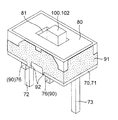
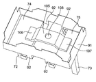
- the third embodiment is a case where the magnetic shield structure according to the present invention is applied to a switch 70 as shown in FIGS.
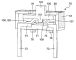
- the switch 70 is formed by a plate-like base 71, a box-shaped case 80, and an operation lever 100 assembled to the box-shaped case 80.
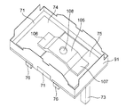
- the plate-like base 71 is integrally formed with a pair of fixed contact terminals 72 and 73 so that the fixed contacts 74 and 75 are exposed at both side edges of the upper surface.
- the plate-like base 71 has four positioning legs 76 protruding between the fixed contact terminals 72 and 73 on the lower surface thereof.
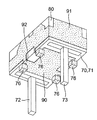
- the plate-like base 71 has a magnetic shield body 90 formed on the lower surface including the positioning leg portions 76 by the MID molding method.
- the box-shaped case 80 has a box shape capable of covering the upper surface of the plate-like base 71, and has an operation hole 81 formed on the ceiling surface thereof.
- the box-shaped case 80 has an annular magnetic shield 91 formed on the outer surface thereof by the MID molding method.
- the magnetic shield body 91 is electrically connected to the magnetic shield body 90 via a connection portion 92. For this reason, the magnetic shield body 91 can be connected to the ground via the magnetic shield body 90 that covers the positioning legs 76 of the plate-like base 71.
- the operation lever 100 has an inverted T-shaped cross section, and a caulking protrusion 101 provided on the lower surface thereof is inserted into the caulking hole 108 of the movable contact piece 105 and fixed.
- the movable contact piece 105 has a cross-sectional shape in which the movable contacts 106 and 107 located at both ends thereof are brought into contact with the fixed contacts 74 and 75, respectively.
- the operation lever 100 protrudes from the operation hole 81 of the box-shaped case 80 so that the operation protrusion 102 provided on the upper surface of the operation lever 100 can be operated.
- the magnetic shield structure according to the present invention is applied to a high frequency connector.
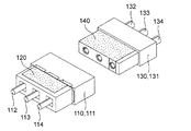
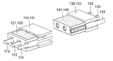
- the high frequency connector includes a plug 110 and a socket 130.
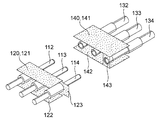
- the plug 110 is formed by integrally molding three connecting pins 112, 113, and 114 arranged side by side on a plug body 111 formed of a resin serving as a dielectric.
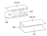
- a magnetic shield 120 is formed on the plug body 111 by the MID molding method. That is, in the magnetic shield body 120, the upper piece 121 and the lower piece 122 arranged so as to sandwich the connection pins 112, 113, 114 from above and below are electrically connected by the connection portion 123.
- the connection part 123 is electrically connected to a connection pin 114 connected to the ground.
- the socket 130 is formed by integrally molding three receiving pins 132, 133, and 134 arranged side by side on a socket main body 131 formed of a resin serving as a dielectric.
- the socket body 131 has a magnetic shield 140 formed by the MID molding method. That is, in the magnetic shield body 140, the upper piece 141 and the lower piece 142 formed so as to sandwich the receiving pins 132, 133, 134 from above and below are electrically connected by the connecting portion 143.
- the connecting portion 143 is electrically connected to a receiving pin 134 connected to the ground.
- the magnetic shield structure according to the present invention is not limited to the above-described electromagnetic relays, switches, and connectors, but may be applied to other electric devices and electronic components having a high-frequency transmission component in a resin housing. .
Landscapes
- Engineering & Computer Science (AREA)
- Power Engineering (AREA)
- Physics & Mathematics (AREA)
- Electromagnetism (AREA)
- Microelectronics & Electronic Packaging (AREA)
- Shielding Devices Or Components To Electric Or Magnetic Fields (AREA)
- Details Of Connecting Devices For Male And Female Coupling (AREA)
Abstract
磁気シールド構造は、誘電体材料からなるハウジングの表面を形成する外面および内面のうち、少なくともいずれか一方に部分的に、金属メッキで形成した磁気シールド体を設けている。
Description
本発明は、磁気シールド構造、特に、ハウジングに金属メッキを施して形成した磁気シールド構造である。
従来、磁気シールド構造の一例としては、例えば、リレー本体に別体の金属ケースを嵌合し、前記リレー本体全体を被覆することにより、磁気シールドされた高周波リレーがある(特許文献1参照)。
しかしながら、前記高周波リレーは、ボディにカバーを被せて構成されたリレー本体に、金属ケースを被せて構成されている。このため、前記高周波リレーは別体の金属ケースを必要とし、部品点数,組立工数が多く、生産性が低い。
また、金属ケースの外形寸法や金属ケースと高周波伝送部品との位置関係が高周波特性に影響を与える。このため、前記金属ケースの製造,組立において高い寸法精度,組立精度を必要とし、製造,組立が容易でない。
そして、前記金属ケースは、前記リレー本体の設置面を除いた露出面全体を被覆する。このため、前記金属ケースが、伝送路構造の特性を却って悪化させる領域や不要な領域を被覆することにより、結果として所望の高周波特性が得られないという問題点がある。
本発明の目的は、前記問題点に鑑み、生産性が高く、製造,組立が容易で、優れた高周波特性を有する磁気シールド構造を提供することである。
本発明に係る磁気シールド構造は、前記課題を解決すべく、誘電体材料からなるハウジングの表面を形成する外面および内面のうち、少なくともいずれか一方に部分的に、金属メッキで形成した磁気シールド体を設けている。
本発明によれば、ハウジングに磁気シールド体を直接設けるので、部品点数,組立工数が少なく、生産性の高い磁気シールド構造が得られる。
また、ハウジングの必要な領域に、磁気シールド体を直接形成する。このため、ハウジングの寸法精度、組立精度のバラツキに基づく高周波特性の低下を防止できる。
そして、ハウジングの必要な領域に限定して磁気シールド体を形成する。このため、従来例のように伝送路構造の特性を却って悪化させる領域や不要な領域に磁気シールド体を形成しない。これにより、結果として優れた高周波特性を有する磁気シールド構造が得られるという効果がある。
また、ハウジングの必要な領域に、磁気シールド体を直接形成する。このため、ハウジングの寸法精度、組立精度のバラツキに基づく高周波特性の低下を防止できる。
そして、ハウジングの必要な領域に限定して磁気シールド体を形成する。このため、従来例のように伝送路構造の特性を却って悪化させる領域や不要な領域に磁気シールド体を形成しない。これにより、結果として優れた高周波特性を有する磁気シールド構造が得られるという効果がある。
本発明の態様に係る磁気シールド構造としては、誘電体材料からなるハウジングの表面を形成する外面および内面のうち、少なくともいずれか一方に部分的に、金属メッキで形成した磁気シールド体を設けている。
本態様によれば、ハウジングに磁気シールド体を直接設けるので、部品点数,組立工数が少なく、生産性の高い磁気シールド構造が得られる。
また、ハウジングの必要な領域に、磁気シールド体を直接形成する。このため、ハウジングの寸法精度、組立精度のバラツキに基づく高周波特性の低下を防止できる。
そして、ハウジングの必要な領域に限定して磁気シールド体を形成する。このため、従来例のように伝送路構造の特性を却って悪化させる領域や不要な領域に磁気シールド体を形成しない。これにより、結果として優れた高周波特性を有する磁気シールド構造が得られるという効果がある。
本態様によれば、ハウジングに磁気シールド体を直接設けるので、部品点数,組立工数が少なく、生産性の高い磁気シールド構造が得られる。
また、ハウジングの必要な領域に、磁気シールド体を直接形成する。このため、ハウジングの寸法精度、組立精度のバラツキに基づく高周波特性の低下を防止できる。
そして、ハウジングの必要な領域に限定して磁気シールド体を形成する。このため、従来例のように伝送路構造の特性を却って悪化させる領域や不要な領域に磁気シールド体を形成しない。これにより、結果として優れた高周波特性を有する磁気シールド構造が得られるという効果がある。
本発明の態様に係る磁気シールド構造としては、前記ハウジングの内面および/または外面のうち、前記ハウジングに配置された高周波伝送路に沿って対向する領域に、前記高周波伝送路の特性インピーダンスが均一になるように前記金属メッキで前記磁気シールド体を設けておいてもよい。
本態様によれば、ハウジングの内面および/または外面の全面に金属メッキで常に磁気シールド体を設ける必要がない。このため、原材料を節約でき、生産性の高い磁気シールド構造が得られる。
本態様によれば、ハウジングの内面および/または外面の全面に金属メッキで常に磁気シールド体を設ける必要がない。このため、原材料を節約でき、生産性の高い磁気シールド構造が得られる。
本発明の他の態様に係る磁気シールド構造としては、前記ハウジングの内面および/または外面のうち、前記ハウジングに配置された高周波伝送路に沿って対向する領域に、前記高周波伝送路の特性インピーダンスが均一になるように前記金属メッキおよび誘電体で前記磁気シールド体を設けておいてもよい。
本態様によれば、ハウジングの内面および/または外面の全面に金属メッキおよび誘電体で磁気シールド体を常に設ける必要がない。このため、原材料を節約でき、生産性の高い磁気シールド構造が得られる。
本態様によれば、ハウジングの内面および/または外面の全面に金属メッキおよび誘電体で磁気シールド体を常に設ける必要がない。このため、原材料を節約でき、生産性の高い磁気シールド構造が得られる。
本発明の別の態様に係る磁気シールド構造としては、前記ハウジングが、ベースと、前記ベースに嵌合するケースとで構成されていてもよい。
本態様によれば、汎用性の高い磁気シールド構造が得られる。
本態様によれば、汎用性の高い磁気シールド構造が得られる。
本発明の新たな態様に係る磁気シールド構造としては、前記ケースの外面の少なくとも一部に、前記磁気シールド体を形成してもよい。また、前記ケースの内面の少なくとも一部に、前記磁気シールド体を形成してもよい。
本態様によれば、必要に応じて必要な領域に磁気シールド体を形成できるので、より一層優れた高周波特性を有する磁気シールド構造が得られる。
本態様によれば、必要に応じて必要な領域に磁気シールド体を形成できるので、より一層優れた高周波特性を有する磁気シールド構造が得られる。
本発明の別の態様に係る磁気シールド構造としては、前記ケースの外面に形成した前記磁気シールド体と、前記ケースの内面に形成した前記磁気シールド体とを前記金属メッキで電気接続してもよい。
本態様によれば、より一層、優れた高周波特性を有する磁気シールド構造が得られる。
本態様によれば、より一層、優れた高周波特性を有する磁気シールド構造が得られる。
本発明の異なる態様に係る磁気シールド構造としては、前記ベースの底面の少なくとも一部に、前記磁気シールド体を設けておいてもよい。
本態様によれば、必要に応じて必要な領域に磁気シールド体を形成できるので、用途の広い磁気シールド構造が得られる。
本態様によれば、必要に応じて必要な領域に磁気シールド体を形成できるので、用途の広い磁気シールド構造が得られる。
本発明の新たな態様に係る磁気シールド構造としては、前記ケースの外面に形成した前記磁気シールド体と、前記ベースの底面に形成した前記磁気シールド体とを前記金属メッキで電気接続してもよい。
本態様によれば、ベースの底面に設けた磁気シールド体を介してグランドに接続できる。
本態様によれば、ベースの底面に設けた磁気シールド体を介してグランドに接続できる。
本発明の他の態様に係る磁気シールド構造としては、前記ハウジングが、プラグ本体と、前記プラグ本体に接続されるソケット本体とで構成されていてもよい。
本態様によれば、汎用性の高い磁気シールド構造が得られる。
本態様によれば、汎用性の高い磁気シールド構造が得られる。
本発明の別の態様に係る磁気シールド構造としては、前記プラグ本体の少なくとも1部に、前記金属メッキで前記磁気シールド体を設けてもよい。また、前記ソケット本体の少なくとも1部に、前記金属メッキで前記磁気シールド体を設けておいてもよい。
本態様によれば、必要に応じて必要な領域に磁気シールド構造を形成できるという効果がある。
本態様によれば、必要に応じて必要な領域に磁気シールド構造を形成できるという効果がある。
本発明の態様に係る電気・電子部品としては、上記の前記磁気シールド構造を備えている。
本態様によれば、上記磁気シールド構造を電磁継電器、スイッチ、コネクタに限らず、樹脂製ハウジング内に高周波伝送部品を備えた他の電気機器、電子部品に適用できる。
本態様によれば、上記磁気シールド構造を電磁継電器、スイッチ、コネクタに限らず、樹脂製ハウジング内に高周波伝送部品を備えた他の電気機器、電子部品に適用できる。
本発明に係る磁気シールド構造の実施形態を図1ないし図25に従って説明する。
(第1実施形態)
第1実施形態は、図1ないし図7に示すように、本発明に係る磁気シールド構造を磁気シールドされた自己保持型の電磁継電器10に適用した場合である。
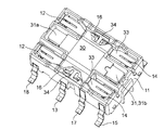
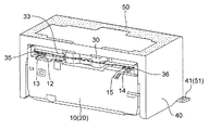
前記電磁継電器10は、図1および図2に示すように、ベース11にケース40を嵌合して形成した内部空間に、可動ブロック30を回動可能に支持してある。なお、説明の便宜上、前記ケース40に設けた磁気シールド体50は散点模様で図示してある。
第1実施形態は、図1ないし図7に示すように、本発明に係る磁気シールド構造を磁気シールドされた自己保持型の電磁継電器10に適用した場合である。
前記電磁継電器10は、図1および図2に示すように、ベース11にケース40を嵌合して形成した内部空間に、可動ブロック30を回動可能に支持してある。なお、説明の便宜上、前記ケース40に設けた磁気シールド体50は散点模様で図示してある。
前記ベース11は、図2ないし図6に示すように、電磁石ブロック20を一体成形したものである。また、前記ベース11は、図2に示すように、その上面の隅部に固定接点12,14を配置してある。前記固定接点12,14は、前記ベース11に一体成形された固定接点端子13,15にそれぞれ接続されている。また、前記ベース11は、その上面の対向する両側縁部に共通接続受け部16を設けてある。前記共通接続受け部16は、前記ベース11に一体成形された共通端子17に接続されている。なお、前記ベース11に一体成形されているコイル端子18は、後述する電磁石ブロック20のコイル22に接続されている。
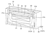
前記電磁石ブロック20は、図3および図5に示すように、断面門型の鉄芯21に絶縁シート(図示せず)を介してコイル22を巻回し、かつ、前記鉄芯21および前記コイル22をスプール23に一体成形したものである。そして、前記鉄芯21の磁極部21a,21bが前記ベース11の上面の両側縁部から露出している(図4)。
また、前記可動ブロック30は、図4に示すように、短冊状の可動鉄片31の下面に板状の永久磁石32を配置するとともに、図2に示すように、前記可動鉄片31の両側に可動接触片33,33を平行に配置し、一体成形したものである。そして、前記可動接触片33は、図2および図5に示すように、その片側縁部から平面略T字形状の接続舌片34を側方に延在してある。前記接続舌片34は、図2に示すように、前記可動ブロック30の両側端面から同一軸心上に突出している。さらに、前記可動接触片33の両端部は、図3に示すように、巾方向に2分割された各分割片に、可動接点35,36をそれぞれ設けたツイン接点構造を有している。
そして、図5に示すように、前記ベース11の前記共通接続受け部16に前記可動ブロック30の前記接続舌片34を溶接一体化することにより、前記可動ブロック30が回動可能に支持される。これにより、可動鉄片31の両端部31a,31bが鉄芯21の磁極部21a,21bに交互に接離可能に対向する。また、可動接触片33の可動接点35,36が、固定接点12,14に交互に接離可能に対向する。
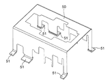
前記ケース40は、前記ベース11に嵌合可能な箱形状を有する樹脂成形品である。そして、前記ケース40は、その外周面に磁気シールド体50を成形回路部品(Molded Interconect Devices:MID)成形法で形成してある。前記MID成形法とは、樹脂と導電素材とを混合した材料で形成した成形品に、予め決められたパターンに基づいてレーザ照射し、樹脂を除去した後、露出する前記導電素材に金属メッキを施すことにより、所望の回路パターンを形成する方法である。また、前記ケース40の開口縁部から延在した端子部41の全表面にも筒状磁気シールド部51が設けられている(図7)。図示しないプリント基板等のグランドに接続するためである。
前記磁気シールド体50は、高周波伝送路において特性インピーダンスにバラツキがあると、高周波信号が漏れやすいという知見に基づいて設けられている。したがって、前記磁気シールド体50は、高周波信号の漏れを低減するため、高周波伝送路における特性インピーダンスのバラツキを小さくするように形成される。
要するに、前記ケース40の外周面全体に金属メッキで磁気シールド体を形成するのではなく、必要な領域に適切な磁気シールド体50を形成する。これにより、前記磁気シールド体50は、例えば、マイクロストリップ構造、ストリップライン構造、および、コプレーナライン構造を構成している。
要するに、前記ケース40の外周面全体に金属メッキで磁気シールド体を形成するのではなく、必要な領域に適切な磁気シールド体50を形成する。これにより、前記磁気シールド体50は、例えば、マイクロストリップ構造、ストリップライン構造、および、コプレーナライン構造を構成している。
前記磁気シールド体50を形成する領域としては、ベースおよびケースからなるハウジングの内面および/または外面のうち、前記ハウジングに設置された高周波伝送路に沿って対向する領域が挙げられる。
より具体的には、高周波伝送路の特性インピーダンスが均一になるように金属メッキおよび/または誘電体を配置,形成することが好ましい。なお、空気も誘電体として考えることは勿論である。
例えば、高周波伝送路の各領域におけるそれぞれの特性インピーダンスが基準値の50Ωに揃うように、金属メッキおよび/または誘電体を配置,形成することが好ましい。高周波伝送路の領域毎に特性インピーダンスに差があると、その差がある領域の境界から高周波が漏れやすく、高周波特性が低下するからである。
より具体的には、高周波伝送路の特性インピーダンスが均一になるように金属メッキおよび/または誘電体を配置,形成することが好ましい。なお、空気も誘電体として考えることは勿論である。
例えば、高周波伝送路の各領域におけるそれぞれの特性インピーダンスが基準値の50Ωに揃うように、金属メッキおよび/または誘電体を配置,形成することが好ましい。高周波伝送路の領域毎に特性インピーダンスに差があると、その差がある領域の境界から高周波が漏れやすく、高周波特性が低下するからである。
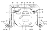
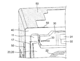
本実施形態におけるマイクロストリップ構造としては、例えば、図6に示すように、高周波伝送路である共通端子17を、誘電体である電磁石ブロック20の樹脂製のスプール23と、磁気シールド体50を設けた誘電体である樹脂製のケース40とで、挟持した構造が挙げられる。
また、ストリップライン構造としては、例えば、図6に示すように、高周波伝送路である可動接触片33の上方に、磁気シールド体50を設けた誘電体である樹脂製のケース40を配置した構造が挙げられる。
そして、コプレーナライン構造としては、例えば、図1に示すように、高周波伝送路であるコイル端子18と、誘電体である樹脂製のケース40の外周面に形成された磁気シールド体50との間に微小な空隙部を形成した構造が挙げられる。固定接点端子13,15および共通端子17も同様に、コプレーナライン構造を構成している。
次に、前述の構成からなる自己保持型の電磁継電器の操作方法を説明する。
例えば、図4に示す前記電磁石ブロック20のコイル22に電圧が印加されていない場合には、鉄芯21の一方の磁極部、例えば、磁極部21aに可動鉄片31の一端部31aが吸着し、磁気回路を構成している。このため、図3に示す可動接触片33の可動接点35が固定接点12に接触し、可動接点36が固定接点14から開離している。
例えば、図4に示す前記電磁石ブロック20のコイル22に電圧が印加されていない場合には、鉄芯21の一方の磁極部、例えば、磁極部21aに可動鉄片31の一端部31aが吸着し、磁気回路を構成している。このため、図3に示す可動接触片33の可動接点35が固定接点12に接触し、可動接点36が固定接点14から開離している。
そして、図4に示す前記永久磁石32の磁力線を打ち消す方向の磁力線が生じるように、前記コイル22に電圧を印加すると、前記永久磁石32の磁力に抗し、図3に示す可動鉄片31の他端部31bが鉄芯21の磁極部21bに吸引される。このため、可動ブロック30が接続舌片34(図5)を中心として回動する。この結果、図3に示す可動接触片33の可動接点36が固定接点14に接触した後、図4に示す可動鉄片31の他端部31bが鉄芯21の磁極部21bに吸着し、磁気回路が形成される。
ついで、前記コイル22に対する電圧の印加を停止しても、前記永久磁石32の磁力により、可動ブロック30は、その状態を維持し続ける。
ついで、前記コイル22に対する電圧の印加を停止しても、前記永久磁石32の磁力により、可動ブロック30は、その状態を維持し続ける。
最後に、図4に示す前記コイル22に、前述の電圧の印加方向と逆方向の電圧を印加する。これにより、発生した磁力線が永久磁石32の磁力線に打ち勝つと、図4に示す可動鉄片31の一端部31aが鉄芯21の磁極部21aに吸引され、可動ブロック30が接続舌片34(図5)を中心として回動する。このため、図3に示す可動接触片33の一端部に設けた可動接点35が固定接点12に接触した後、図4に示す可動鉄片31の一端部31aが鉄芯21の磁極部21aに吸着する。
以後、同様な操作を繰り返すことにより、接点が切り換えられる。
以後、同様な操作を繰り返すことにより、接点が切り換えられる。
(実施例)
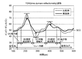
本実施形態に係る磁気シールド体50を備えた電磁継電器の高周波特性について解析を行った。解析結果を図8のグラフ図に示す。
本実施形態に係る磁気シールド体50を備えた電磁継電器の高周波特性について解析を行った。解析結果を図8のグラフ図に示す。
(比較例)
第1実施形態と同一の電磁継電器のケースに金属メッキの磁気シールド体を形成せず、前記ケース全体を被覆する金属ケースを被せたものを比較例とした。他は前述の第1実施形態と同一の条件で高周波特性を解析した。解析結果を図8のグラフ図で示す。
第1実施形態と同一の電磁継電器のケースに金属メッキの磁気シールド体を形成せず、前記ケース全体を被覆する金属ケースを被せたものを比較例とした。他は前述の第1実施形態と同一の条件で高周波特性を解析した。解析結果を図8のグラフ図で示す。
なお、図8は時間領域反射手法(Time Domain Refrectometry:TDR)によって測定されている。前記TDR手法とは、高速のパルスあるいはステップ信号入力を被測定物に印加し、返ってくる反射波形を測定する手法をいう。前記反射波形から高周波伝送路の経路における特性インピーダンスを検出できる。そして、図8において、
(A)端子部とは、図2における共通端子17のうち、プリント基板に表面実装される先端領域だけの特性インピーダンスを示している。
(B)固定接点端子とは、前記共通端子17のうち、前記先端領域の境界から共通接続受け部16まで領域における特性インピーダンスを示している。
(C)可動接触片とは、可動接触片33の接続舌片34の基部から可動接点36までの領域における特性インピーダンスを示している。
(D)固定接点端子とは、固定接点端子15のうち、前記固定接点端子15に設けた固定接点14からプリント基板に表面実装される先端領域の境界までの領域における特性インピーダンスを示している。
(E)端子部とは、前記固定接点端子15のうち、プリント基板に表面実装される先端領域だけの特性インピーダンスを示している。
(A)端子部とは、図2における共通端子17のうち、プリント基板に表面実装される先端領域だけの特性インピーダンスを示している。
(B)固定接点端子とは、前記共通端子17のうち、前記先端領域の境界から共通接続受け部16まで領域における特性インピーダンスを示している。
(C)可動接触片とは、可動接触片33の接続舌片34の基部から可動接点36までの領域における特性インピーダンスを示している。
(D)固定接点端子とは、固定接点端子15のうち、前記固定接点端子15に設けた固定接点14からプリント基板に表面実装される先端領域の境界までの領域における特性インピーダンスを示している。
(E)端子部とは、前記固定接点端子15のうち、プリント基板に表面実装される先端領域だけの特性インピーダンスを示している。
図8から明らかなように、実施例の反射波形が比較例の反射波形よりも特性インピーダンス(50Ω)に接近していることが判った。これにより、比較例よりも実施例の方が特性インピーダンスに対するバラツキが小さく、高周波信号の漏れが少ないことが判明した。
(第2実施形態)
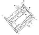
第2実施形態は、図9ないし図15に示すように、前述の第1実施形態と同様、本発明に係る磁気シールド構造を電磁継電器のケース40に適用した場合である。第1実施形態と異なる点は前記ケース40の内周面にも磁気シールド体60をMID成形法で形成した点である。このため、第1実施形態と異なる点について説明し、同一部分については同一番号を附して説明を省略する。
第2実施形態は、図9ないし図15に示すように、前述の第1実施形態と同様、本発明に係る磁気シールド構造を電磁継電器のケース40に適用した場合である。第1実施形態と異なる点は前記ケース40の内周面にも磁気シールド体60をMID成形法で形成した点である。このため、第1実施形態と異なる点について説明し、同一部分については同一番号を附して説明を省略する。
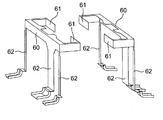
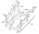
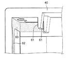
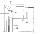
前記磁気シールド体60は、前記ケース40の内周面の対向する隅部にそれぞれ設けられている。特に、前記磁気シールド体60は、図11に示すように、両端部から一対の腕部61を延在している。前記腕部61は第1実施形態の可動接触片33の両端部を囲む形状となっている。また、前記磁気シールド体60は、下方に向けて延在する脚部62を介し、前記磁気シールド体50の筒状磁気シールド部51に電気接続されている。
本実施形態によれば、図14および図15に示すように、誘電体である樹脂製のケースの内面に取り付けた磁気シールド体60と、その腕部61との間に、微小な空隙を形成するように可動接触片33の両端部を配置してある。これにより、第1実施形態と同様なコプレーナライン構造を構成している。
したがって、第2実施形態によれば、磁気シールド体50だけでなく、磁気シールド体60を設けることにより、特性インピーダンスが調整しやすい。このため、高周波伝送路における特性インピーダンスのバラツキをより一層低減しやすくなり、高周波特性を改善できる。このため、設計の自由度が広がり、用途がより一層拡大するという利点がある。
したがって、第2実施形態によれば、磁気シールド体50だけでなく、磁気シールド体60を設けることにより、特性インピーダンスが調整しやすい。このため、高周波伝送路における特性インピーダンスのバラツキをより一層低減しやすくなり、高周波特性を改善できる。このため、設計の自由度が広がり、用途がより一層拡大するという利点がある。
(第3実施形態)
第3実施形態は、図16ないし図22に示すように、本発明に係る磁気シールド構造をスイッチ70に適用した場合である。前記スイッチ70は、板状ベース71と、箱形ケース80と、前記箱形ケース80に組み付けられた操作レバー100とで、形成されている。
第3実施形態は、図16ないし図22に示すように、本発明に係る磁気シールド構造をスイッチ70に適用した場合である。前記スイッチ70は、板状ベース71と、箱形ケース80と、前記箱形ケース80に組み付けられた操作レバー100とで、形成されている。
前記板状ベース71は、図18に示すように、その上面の両側縁部に固定接点74,75が露出するように一対の固定接点端子72,73を一体成形してある。また、前記板状ベース71は、その下面のうち、前記固定接点端子72,73の間に4つの位置決め用脚部76を突設してある。そして、前記板状ベース71は、前記位置決め用脚部76を含む下面に磁気シールド体90をMID成形法で形成してある。
前記箱形ケース80は、前記板状ベース71の上面を被覆可能な箱形状を有し、その天井面に操作孔81を形成してある。また、前記箱形ケース80は、その外側面に環状の磁気シールド体91をMID成形法で形成してある。そして、前記磁気シールド体91は接続部92を介して前記磁気シールド体90に電気接続されている。このため、前記磁気シールド体91は、前記板状ベース71の位置決め用脚部76を被覆する磁気シールド体90を介してグランドに接続できる。
操作レバー100は、図18に示すように、断面逆T字形状を有し、かつ、その下面に設けたカシメ用突起101を可動接触片105のカシメ孔108に挿入して固定してある。前記可動接触片105は、その両端部に位置する可動接点106,107を、前記固定接点74,75にそれぞれ接触する断面形状を有している。そして、前記操作レバー100は、その上面に突設した操作突部102を前記箱形ケース80の操作孔81から操作可能に突出している。
したがって、前記操作レバー100の操作突部102をスライド移動させることにより、可動接点106,107が固定接点74,75にそれぞれ接触する。そして、高周波信号が固定接点端子72、可動接触片105および固定接点端子73に流れても、磁気シールド体90,91で磁気シールドされている。このため、高周波信号が漏れないだけでなく、外部信号の侵入をも防止できるという利点がある。
(第4実施形態)
第4実施形態は、図22ないし図25に示すように、本発明に係る磁気シールド構造を高周波用コネクタに適用した場合である。そして、前記高周波用コネクタは、プラグ110と、ソケット130とで構成されている。
第4実施形態は、図22ないし図25に示すように、本発明に係る磁気シールド構造を高周波用コネクタに適用した場合である。そして、前記高周波用コネクタは、プラグ110と、ソケット130とで構成されている。
前記プラグ110は、並設した3本の接続ピン112,113,114を、誘電体となる樹脂で成形されたプラグ本体111に一体成形したものである。そして、前記プラグ本体111には磁気シールド体120をMID成形法で形成してある。
すなわち、前記磁気シールド体120は、前記接続ピン112,113,114を上下から挟むように配置した上片部121と下片部122とを、接続部123で電気接続してある。前記接続部123はグランドに接続される接続ピン114に電気接続されている。
すなわち、前記磁気シールド体120は、前記接続ピン112,113,114を上下から挟むように配置した上片部121と下片部122とを、接続部123で電気接続してある。前記接続部123はグランドに接続される接続ピン114に電気接続されている。
また、前記ソケット130は、並設した3本の受入れピン132,133,134を、誘電体となる樹脂で成形されたソケット本体131に一体成形したものである。そして、前記ソケット本体131は磁気シールド体140をMID成形法で形成してある。
すなわち、前記磁気シールド体140は、前記受入れピン132,133,134を上下から挟むように形成した上片部141と下片部142とを、接続部143で電気接続してある。前記接続部143はグランドに接続される受入れピン134に電気接続されている。
すなわち、前記磁気シールド体140は、前記受入れピン132,133,134を上下から挟むように形成した上片部141と下片部142とを、接続部143で電気接続してある。前記接続部143はグランドに接続される受入れピン134に電気接続されている。
本発明に係る磁気シールド構造は、前述の電磁継電器、スイッチ、コネクタに限らず、樹脂製ハウジング内に高周波伝送部品を備えた他の電気機器、電子部品に適用してもよいことは勿論である。
10 電磁継電器
11 ベース
12 固定接点
13 固定接点端子
14 固定接点
15 固定接点端子
16 共通接続受け部
17 共通端子
18 コイル端子
20 電磁石ブロック
21 鉄芯
22 コイル
23 スプール
30 可動ブロック
31 可動鉄片
32 永久磁石
33 可動接触片
40 ケース
41 端子部
50 磁気シールド体
51 筒状磁気シールド部
60 磁気シールド体
61 腕部
62 脚部
70 スイッチ
71 板状ベース
72 固定接点端子
73 固定接点端子
74 固定接点
75 固定接点
76 位置決め用脚部
80 箱形ケース
81 操作孔
90 磁気シールド体
91 磁気シールド体
92 接続部
110 プラグ
111 プラグ本体
120 磁気シールド体
121 上片部
122 下片部
123 接続部
130 ソケット
131 ソケット本体
140 磁気シールド体
141 上片部
142 下片部
143 接続部
11 ベース
12 固定接点
13 固定接点端子
14 固定接点
15 固定接点端子
16 共通接続受け部
17 共通端子
18 コイル端子
20 電磁石ブロック
21 鉄芯
22 コイル
23 スプール
30 可動ブロック
31 可動鉄片
32 永久磁石
33 可動接触片
40 ケース
41 端子部
50 磁気シールド体
51 筒状磁気シールド部
60 磁気シールド体
61 腕部
62 脚部
70 スイッチ
71 板状ベース
72 固定接点端子
73 固定接点端子
74 固定接点
75 固定接点
76 位置決め用脚部
80 箱形ケース
81 操作孔
90 磁気シールド体
91 磁気シールド体
92 接続部
110 プラグ
111 プラグ本体
120 磁気シールド体
121 上片部
122 下片部
123 接続部
130 ソケット
131 ソケット本体
140 磁気シールド体
141 上片部
142 下片部
143 接続部
Claims (13)
- 誘電体材料からなるハウジングの表面を形成する外面および内面のうち、少なくともいずれか一方に部分的に、金属メッキで形成した磁気シールド体を設けたことを特徴とする磁気シールド構造。
- 前記ハウジングの内面および/または外面のうち、前記ハウジングに配置された高周波伝送路に沿って対向する領域に、前記高周波伝送路の特性インピーダンスが均一になるように前記金属メッキで前記磁気シールド体を設けたことを特徴とする請求項1に記載の磁気シールド構造。
- 前記ハウジングの内面および/または外面のうち、前記ハウジングに配置された高周波伝送路に沿って対向する領域に、前記高周波伝送路の特性インピーダンスが均一になるように前記金属メッキおよび誘電体で前記磁気シールド体を設けたことを特徴とする請求項1または2に記載の磁気シールド構造。
- 前記ハウジングが、ベースと、前記ベースに嵌合するケースとからなることを特徴とする請求項1ないし3のいずれか1項に記載の磁気シールド構造。
- 前記ケースの外面の少なくとも一部に、前記磁気シールド体を形成したことを特徴とする請求項4に記載の磁気シールド構造。
- 前記ケースの内面の少なくとも一部に、前記磁気シールド体を形成したことを特徴とする請求項4または5に記載の磁気シールド構造。
- 前記ケースの外面に形成した前記磁気シールド体と、前記ケースの内面に形成した前記磁気シールド体とを金属メッキで電気接続したことを特徴とする請求項4ないし6のいずれか1項に記載の磁気シールド構造。
- 前記ベースの底面の少なくとも一部に、前記磁気シールド体を設けたことを特徴とする請求項4ないし7のいずれか1項に記載の磁気シールド構造。
- 前記ケースの外面に形成した前記磁気シールド体と、前記ベースの底面に形成した前記磁気シールド体とを前記金属メッキで電気接続したことを特徴とする請求項4ないし8のいずれか1項に記載の磁気シールド構造。
- 前記ハウジングが、プラグ本体と、前記プラグ本体に接続されるソケット本体とからなることを特徴とする請求項1ないし3のいずれか1項に記載の磁気シールド構造。
- 前記プラグ本体の少なくとも1部に、前記金属メッキで前記磁気シールド体を設けたことを特徴とする請求項10に記載の磁気シールド構造。
- 前記ソケット本体の少なくとも1部に、前記金属メッキで前記磁気シールド体を設けたことを特徴とする請求項10または11に記載の磁気シールド構造。
- 請求項1から12のいずれか一項に記載の前記磁気シールド構造を備えた、電気・電子部品。
Priority Applications (3)
| Application Number | Priority Date | Filing Date | Title |
|---|---|---|---|
| DE112016004126.8T DE112016004126T5 (de) | 2015-09-11 | 2016-08-29 | Magnetische Abschirmungsstruktur |
| CN201680040711.9A CN107851535A (zh) | 2015-09-11 | 2016-08-29 | 磁屏蔽结构 |
| US15/876,069 US20180144892A1 (en) | 2015-09-11 | 2018-01-19 | Magnetic shield structure |
Applications Claiming Priority (2)
| Application Number | Priority Date | Filing Date | Title |
|---|---|---|---|
| JP2015179234A JP2017054757A (ja) | 2015-09-11 | 2015-09-11 | 磁気シールド構造 |
| JP2015-179234 | 2015-09-11 |
Related Child Applications (1)
| Application Number | Title | Priority Date | Filing Date |
|---|---|---|---|
| US15/876,069 Continuation US20180144892A1 (en) | 2015-09-11 | 2018-01-19 | Magnetic shield structure |
Publications (1)
| Publication Number | Publication Date |
|---|---|
| WO2017043348A1 true WO2017043348A1 (ja) | 2017-03-16 |
Family
ID=58239625
Family Applications (1)
| Application Number | Title | Priority Date | Filing Date |
|---|---|---|---|
| PCT/JP2016/075114 Ceased WO2017043348A1 (ja) | 2015-09-11 | 2016-08-29 | 磁気シールド構造 |
Country Status (5)
| Country | Link |
|---|---|
| US (1) | US20180144892A1 (ja) |
| JP (1) | JP2017054757A (ja) |
| CN (1) | CN107851535A (ja) |
| DE (1) | DE112016004126T5 (ja) |
| WO (1) | WO2017043348A1 (ja) |
Cited By (1)
| Publication number | Priority date | Publication date | Assignee | Title |
|---|---|---|---|---|
| EP3518257A1 (en) * | 2018-01-26 | 2019-07-31 | FRIWO Gerätebau GmbH | Transformer unit for a resonant converter |
Families Citing this family (4)
| Publication number | Priority date | Publication date | Assignee | Title |
|---|---|---|---|---|
| JP6451472B2 (ja) * | 2015-04-13 | 2019-01-16 | オムロン株式会社 | 電子機器 |
| JP6753339B2 (ja) * | 2017-03-13 | 2020-09-09 | オムロン株式会社 | 高周波リレー |
| JP2025045918A (ja) * | 2023-09-20 | 2025-04-02 | オムロン株式会社 | 電磁継電器 |
| JP2025045916A (ja) * | 2023-09-20 | 2025-04-02 | オムロン株式会社 | 回路部品 |
Citations (6)
| Publication number | Priority date | Publication date | Assignee | Title |
|---|---|---|---|---|
| JPS5834273U (ja) * | 1981-08-28 | 1983-03-05 | オムロン株式会社 | 高周波用開閉器 |
| JPS61127197A (ja) * | 1984-11-24 | 1986-06-14 | 凸版印刷株式会社 | 電磁波シ−ルド性を有するプラスチツクハウジング |
| JPH0963703A (ja) * | 1995-08-24 | 1997-03-07 | Sankyo Kasei Co Ltd | 端子間シールドコネクタとその製法 |
| JPH09274969A (ja) * | 1996-04-02 | 1997-10-21 | Toshiba Corp | コネクタ |
| JPH11144592A (ja) * | 1997-11-07 | 1999-05-28 | Nec Corp | 電磁継電器 |
| JP2003222639A (ja) * | 2002-01-30 | 2003-08-08 | Iwatsu Electric Co Ltd | 高周波入力切換回路 |
Family Cites Families (11)
| Publication number | Priority date | Publication date | Assignee | Title |
|---|---|---|---|---|
| JP2921248B2 (ja) * | 1992-02-14 | 1999-07-19 | 日本電気株式会社 | コネクタ |
| JP2000100302A (ja) * | 1998-09-25 | 2000-04-07 | Matsushita Electric Works Ltd | 高周波リレー |
| JP2000340084A (ja) | 1999-05-26 | 2000-12-08 | Matsushita Electric Works Ltd | 高周波リレー |
| TWI279080B (en) * | 2001-09-20 | 2007-04-11 | Nec Corp | Shielded strip line device and method of manufacture thereof |
| JP2006024824A (ja) * | 2004-07-09 | 2006-01-26 | Tatsuta System Electronics Kk | インピーダンスコントロールフィルム、インピーダンスコントロールシールドフィルム及びそれを用いた配線板 |
| CN2786751Y (zh) * | 2005-02-01 | 2006-06-07 | 上海环达计算机科技有限公司 | 具有电磁波屏蔽的薄型硬盘组装结构 |
| JP2007115771A (ja) * | 2005-10-18 | 2007-05-10 | Nec System Technologies Ltd | Lsiピン |
| JP2008243665A (ja) * | 2007-03-28 | 2008-10-09 | Totoku Electric Co Ltd | 特性インピーダンスの整合が可能なシールドフレキシブルフラットケーブル |
| EP2485253B1 (en) * | 2009-09-29 | 2019-12-18 | Kyocera Corporation | Device housing package |
| WO2012030367A1 (en) * | 2010-08-31 | 2012-03-08 | 3M Innovative Properties Company | Shielded electrical cable in twinaxial configuration |
| CA2809345A1 (en) * | 2010-08-31 | 2012-03-08 | 3M Innovative Properties Company | Connector arrangements for shielded electrical cables |
-
2015
- 2015-09-11 JP JP2015179234A patent/JP2017054757A/ja active Pending
-
2016
- 2016-08-29 DE DE112016004126.8T patent/DE112016004126T5/de not_active Withdrawn
- 2016-08-29 CN CN201680040711.9A patent/CN107851535A/zh active Pending
- 2016-08-29 WO PCT/JP2016/075114 patent/WO2017043348A1/ja not_active Ceased
-
2018
- 2018-01-19 US US15/876,069 patent/US20180144892A1/en not_active Abandoned
Patent Citations (6)
| Publication number | Priority date | Publication date | Assignee | Title |
|---|---|---|---|---|
| JPS5834273U (ja) * | 1981-08-28 | 1983-03-05 | オムロン株式会社 | 高周波用開閉器 |
| JPS61127197A (ja) * | 1984-11-24 | 1986-06-14 | 凸版印刷株式会社 | 電磁波シ−ルド性を有するプラスチツクハウジング |
| JPH0963703A (ja) * | 1995-08-24 | 1997-03-07 | Sankyo Kasei Co Ltd | 端子間シールドコネクタとその製法 |
| JPH09274969A (ja) * | 1996-04-02 | 1997-10-21 | Toshiba Corp | コネクタ |
| JPH11144592A (ja) * | 1997-11-07 | 1999-05-28 | Nec Corp | 電磁継電器 |
| JP2003222639A (ja) * | 2002-01-30 | 2003-08-08 | Iwatsu Electric Co Ltd | 高周波入力切換回路 |
Cited By (1)
| Publication number | Priority date | Publication date | Assignee | Title |
|---|---|---|---|---|
| EP3518257A1 (en) * | 2018-01-26 | 2019-07-31 | FRIWO Gerätebau GmbH | Transformer unit for a resonant converter |
Also Published As
| Publication number | Publication date |
|---|---|
| US20180144892A1 (en) | 2018-05-24 |
| DE112016004126T5 (de) | 2018-05-24 |
| CN107851535A (zh) | 2018-03-27 |
| JP2017054757A (ja) | 2017-03-16 |
Similar Documents
| Publication | Publication Date | Title |
|---|---|---|
| US11239616B2 (en) | Coaxial connector | |
| US20180144892A1 (en) | Magnetic shield structure | |
| US6806801B2 (en) | High frequency relay | |
| US6809255B1 (en) | Radio frequency ground shield | |
| EP0918346B1 (en) | Switch for high frequency | |
| US9070959B2 (en) | Connection unit | |
| JP2021026981A (ja) | ヘッダ及びこれを用いたコネクタ | |
| JPWO1998007169A1 (ja) | 高周波用開閉器 | |
| JP6631339B2 (ja) | 高周波リレー | |
| US6780055B2 (en) | Terminal structure of high frequency signal transmitting part | |
| JP6287904B2 (ja) | 誘電体導波管共振器、誘電体導波管入出力構造および誘電体導波管フィルタ | |
| US10090128B2 (en) | Switch for switching between different high frequency signals | |
| CN112582219B (zh) | 继电器 | |
| US9867281B2 (en) | Assembly comprising a hyperfrequency component and a printed circuit | |
| JP2001257502A (ja) | 高周波用開閉器およびその接続構造 | |
| US20180145387A1 (en) | Switch for switchable attenuator and high frequency switchable attenuator | |
| US20180144897A1 (en) | Force-distance controlled mechanical switch | |
| TWI639173B (zh) | High frequency relay | |
| JPH0612957A (ja) | リレー | |
| JP2005184676A (ja) | 非可逆回路素子 | |
| JP3663338B2 (ja) | 高周波リレーの実装方法および高周波リレーの実装に用いるケース | |
| JP3596550B2 (ja) | 高周波リレー | |
| CN106356601B (zh) | 电介质波导管的输入输出连接构造 | |
| TW202514686A (zh) | 電磁繼電器 | |
| JP2010226552A (ja) | 伝送線路 |
Legal Events
| Date | Code | Title | Description |
|---|---|---|---|
| 121 | Ep: the epo has been informed by wipo that ep was designated in this application |
Ref document number: 16844210 Country of ref document: EP Kind code of ref document: A1 |
|
| WWE | Wipo information: entry into national phase |
Ref document number: 112016004126 Country of ref document: DE |
|
| 122 | Ep: pct application non-entry in european phase |
Ref document number: 16844210 Country of ref document: EP Kind code of ref document: A1 |