WO2017043088A1 - Induction heating power supply apparatus - Google Patents
Induction heating power supply apparatus Download PDFInfo
- Publication number
- WO2017043088A1 WO2017043088A1 PCT/JP2016/004105 JP2016004105W WO2017043088A1 WO 2017043088 A1 WO2017043088 A1 WO 2017043088A1 JP 2016004105 W JP2016004105 W JP 2016004105W WO 2017043088 A1 WO2017043088 A1 WO 2017043088A1
- Authority
- WO
- WIPO (PCT)
- Prior art keywords
- pair
- bus bars
- power supply
- conductors
- capacitor
- Prior art date
Links
- 238000010438 heat treatment Methods 0.000 title claims abstract description 33
- 230000006698 induction Effects 0.000 title claims abstract description 24
- 239000003990 capacitor Substances 0.000 claims abstract description 41
- 238000009499 grossing Methods 0.000 claims abstract description 30
- 239000012212 insulator Substances 0.000 claims abstract description 28
- 239000004020 conductor Substances 0.000 claims description 54
- 239000004065 semiconductor Substances 0.000 description 31
- 230000003071 parasitic effect Effects 0.000 description 7
- 238000010586 diagram Methods 0.000 description 4
- XUIMIQQOPSSXEZ-UHFFFAOYSA-N Silicon Chemical compound [Si] XUIMIQQOPSSXEZ-UHFFFAOYSA-N 0.000 description 1
- 229910000831 Steel Inorganic materials 0.000 description 1
- 241001125929 Trisopterus luscus Species 0.000 description 1
- 239000003985 ceramic capacitor Substances 0.000 description 1
- 230000005669 field effect Effects 0.000 description 1
- 239000000463 material Substances 0.000 description 1
- 238000000034 method Methods 0.000 description 1
- 229910052710 silicon Inorganic materials 0.000 description 1
- 239000010703 silicon Substances 0.000 description 1
- HBMJWWWQQXIZIP-UHFFFAOYSA-N silicon carbide Chemical compound [Si+]#[C-] HBMJWWWQQXIZIP-UHFFFAOYSA-N 0.000 description 1
- 239000010959 steel Substances 0.000 description 1
Images


Classifications
-
- H—ELECTRICITY
- H02—GENERATION; CONVERSION OR DISTRIBUTION OF ELECTRIC POWER
- H02M—APPARATUS FOR CONVERSION BETWEEN AC AND AC, BETWEEN AC AND DC, OR BETWEEN DC AND DC, AND FOR USE WITH MAINS OR SIMILAR POWER SUPPLY SYSTEMS; CONVERSION OF DC OR AC INPUT POWER INTO SURGE OUTPUT POWER; CONTROL OR REGULATION THEREOF
- H02M7/00—Conversion of AC power input into DC power output; Conversion of DC power input into AC power output
- H02M7/003—Constructional details, e.g. physical layout, assembly, wiring or busbar connections
-
- H—ELECTRICITY
- H05—ELECTRIC TECHNIQUES NOT OTHERWISE PROVIDED FOR
- H05B—ELECTRIC HEATING; ELECTRIC LIGHT SOURCES NOT OTHERWISE PROVIDED FOR; CIRCUIT ARRANGEMENTS FOR ELECTRIC LIGHT SOURCES, IN GENERAL
- H05B6/00—Heating by electric, magnetic or electromagnetic fields
- H05B6/02—Induction heating
- H05B6/04—Sources of current
-
- H—ELECTRICITY
- H02—GENERATION; CONVERSION OR DISTRIBUTION OF ELECTRIC POWER
- H02M—APPARATUS FOR CONVERSION BETWEEN AC AND AC, BETWEEN AC AND DC, OR BETWEEN DC AND DC, AND FOR USE WITH MAINS OR SIMILAR POWER SUPPLY SYSTEMS; CONVERSION OF DC OR AC INPUT POWER INTO SURGE OUTPUT POWER; CONTROL OR REGULATION THEREOF
- H02M1/00—Details of apparatus for conversion
- H02M1/32—Means for protecting converters other than automatic disconnection
-
- H—ELECTRICITY
- H02—GENERATION; CONVERSION OR DISTRIBUTION OF ELECTRIC POWER
- H02M—APPARATUS FOR CONVERSION BETWEEN AC AND AC, BETWEEN AC AND DC, OR BETWEEN DC AND DC, AND FOR USE WITH MAINS OR SIMILAR POWER SUPPLY SYSTEMS; CONVERSION OF DC OR AC INPUT POWER INTO SURGE OUTPUT POWER; CONTROL OR REGULATION THEREOF
- H02M7/00—Conversion of AC power input into DC power output; Conversion of DC power input into AC power output
- H02M7/42—Conversion of DC power input into AC power output without possibility of reversal
- H02M7/44—Conversion of DC power input into AC power output without possibility of reversal by static converters
- H02M7/48—Conversion of DC power input into AC power output without possibility of reversal by static converters using discharge tubes with control electrode or semiconductor devices with control electrode
- H02M7/53—Conversion of DC power input into AC power output without possibility of reversal by static converters using discharge tubes with control electrode or semiconductor devices with control electrode using devices of a triode or transistor type requiring continuous application of a control signal
- H02M7/537—Conversion of DC power input into AC power output without possibility of reversal by static converters using discharge tubes with control electrode or semiconductor devices with control electrode using devices of a triode or transistor type requiring continuous application of a control signal using semiconductor devices only, e.g. single switched pulse inverters
- H02M7/5387—Conversion of DC power input into AC power output without possibility of reversal by static converters using discharge tubes with control electrode or semiconductor devices with control electrode using devices of a triode or transistor type requiring continuous application of a control signal using semiconductor devices only, e.g. single switched pulse inverters in a bridge configuration
Definitions
- the present invention relates to an induction heating power supply apparatus.
- Induction heating is used as a heating method in a treat treatment of steel workpieces.
- AC power is applied to a heating coil to cause the heating coil to generate a magnetic field, and a workpiece placed in the magnetic field is heated by electric current induced in the workpiece.
- a related art power supply apparatus for supplying AC power to such a heating coil has a converter to convert AC power of a commercial power supply to DC power, a capacitor to smooth pulsating current of the DC power, and an inverter to convert the smoothed DC power back to AC power to generate high frequency AC power to be supplied to the heating coil (see, e.g., JP 2009-277577A).
- the inverter typically has a bridge circuit including a plurality of power semiconductor devices capable of performing a high speed switching operation to produce high frequency AC power
- the high speed switching operation of a power semiconductor device causes a rapid change in electric current flowing in the power semiconductor device.
- the current change di/dt produces surge voltage Lxdi/dt between terminals of the power semiconductor device due to a parasitic inductance L of a conductive path between the power semiconductor device and the capacitor serving as a voltage source.
- Illustrative aspects of the present invention provide an induction heating power supply apparatus in which surge voltage is suppressed to improve a protection of an inverter.
- an induction heating power supply apparatus includes a smoothing section configured to smooth pulsating current of DC power output from a DC power supply section, and an inverter configured to convert the DC power smoothed by the smoothing section to AC power.
- the smoothing section includes a pair of bus bars connected to the inverter and at least one capacitor connected to the pair of bus bars.
- Each of the bus bars has an external surface extending in a current flow direction.
- the external surface includes at least one flat face having a larger surface dimension than another face of the external surface in a direction perpendicular to the current flow direction.
- the pair of bus bars are arranged in a layered manner such that the flat faces of the pair of bus bars are opposed to each other and such that an insulator is sandwiched between the flat faces of the pair of bus bars.
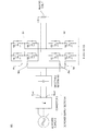
- Fig. 1 is a circuit diagram of an induction heating power supply apparatus according to an embodiment of the present invention.
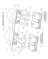
- Fig. 2 is a perspective view illustrating an example of a configuration of a smoothing section of the induction heating power supply apparatus of Fig. 1.
- Fig. 3 is an exploded perspective view of the smoothing section of Fig. 2.
- Fig. 4 is a sectional view of the smoothing section of Fig. 2.
- Fig. 5 is a perspective view of a reference example of the smoothing section.
- Fig. 6 is a perspective view of another reference example of the smoothing section.
- Fig. 7 is a circuit diagram of an induction heating power supply apparatus according to another embodiment of the present invention.
- Fig. 1 is a circuit diagram of an induction heating power supply apparatus according to another embodiment of the present invention.
- Fig. 1 is a circuit diagram of an induction heating power supply apparatus according to another embodiment of the present invention.
- Fig. 1 is a circuit diagram of an induction heating power supply apparatus
- FIG. 8 is a circuit diagram of an induction heating power supply apparatus according to another embodiment of the present invention.
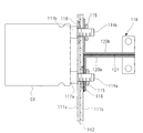
- Fig. 9 is a perspective view illustrating an example of a configuration of a smoothing section of the induction heating power supply apparatus of Fig. 8.
- Fig. 10 is a sectional view of the smoothing section of Fig. 9.
- Fig. 11 is a circuit diagram of an induction heating power supply apparatus according to another embodiment of the present invention..
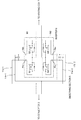
- Fig. 1 illustrates an induction heating power supply apparatus 1 according to an embodiment of the present invention.
- the induction heating power supply apparatus 1 has a DC power supply section 4, a smoothing section 5 and an inverter 6.
- the DC power supply section 4 includes a converter 3 configured to convert AC power supplied from a commercial AC power supply 2 to DC power.
- the smoothing section 5 is configured to smooth pulsating current of the DC power output from the DC power supply section 4.
- the inverter 6 is configured to convert the DC power smoothed by the smoothing section 5 to high frequency AC power.
- the inverter 6 has an arm including power semiconductor devices Q1, Q2 connected in series, and another arm including power semiconductor devices Q3, Q4 also connected in series.
- the invert 6 is configured as a full bridge circuit so that a series connection point between the power semiconductor devices in each of the arms serves as an output terminal.
- Freewheel diodes D are connected in parallel with the power semiconductor devices Q1, Q2, Q3, Q4 respectively.
- various power semiconductor devices which can perform switching operation, such as an insulated gate bipolar transistor (IGBT) and a metal-oxide-semiconductor field-effect transistor (MOSFET) may be used as each power semiconductor device.
- IGBT insulated gate bipolar transistor
- MOSFET metal-oxide-semiconductor field-effect transistor
- examples of the material of the power semiconductor device may include silicon (Si) and silicon carbide (SiC).
- a heating coil 7 is connected between the series connection point of the power semiconductor devices Q1, Q2 and the series connection point of the power semiconductor devices Q3, Q4 so that high frequency power is supplied to the heating coil 7 by the switching operations of the power semiconductor devices Q1, Q2, Q3, Q4.
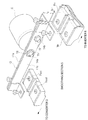
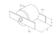
- Figs. 2 to 4 illustrate an example of a configuration of the smoothing section 5.
- the smoothing section 5 includes a pair of bus bars 11a, 11b, and at least one capacitor C connected to the pair of bus bars 11a, 11b.
- Each of the bus bars 11a, 11b is a flat plate conductor having a pair of flat plate faces and a pair of flat side faces, the pair of flat plate faces and the pair of flat side faces forming the external surface of the conductor extending in a current flow direction (the longitudinal direction).
- the bus bars 11a, 11b are arranged in a layered manner such that the flat plate faces of the bus bars 11a, 11b or the flat side faces of the bus bars 11a, 11b, those having relatively large surface dimension in a direction (width direction) perpendicular to the current flow direction are opposed to each other and such that an insulator sheet 12 is sandwiched between the bus bars 11a, 11b.
- One end portion of the bus bar 11a is connected to a positive electrode Pout of an output terminal of the converter 3 while the other end portion of the bus bar 11a is connected to a positive electrode Pin of an input terminal of the inverter 6.
- One end portion of the bus bar 11b is connected to a negative electrode Nout of an output terminal of the converter 3 while the other end portion of the bus bar 11b is connected to a negative electrode Nin of an input terminal of the inverter 6.
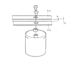
- a pair of terminals 14a, 14b of the capacitor C connected to the bus bars 11a, 11b are formed as screw terminals and arranged side by side on one side of the capacitor C.
- the terminals 14a, 14b are arranged to extend through the bus bars 11a, 11b and the insulator 12 in a direction in which the bus bars 11a, 11b and the insulator 12 are layered in the order of the bus bar 11a, the insulator 12 and the bus bar 11b.
- Nuts 15 are screwed onto distal end portions of the terminals 14a, 14b respectively so that the capacitor C is fixed to the bus bars 11a, 11b.
- the terminal 14a and the nut 15 screwed to the terminal 14a are electrically insulated from the bus bar 11b by an insulating washer 16.
- a large-diameter flange portion 17a formed in a base end portion of the terminal 14a makes contact with the bus bar 11a so that the terminal 14a and the bus bar 11a are electrically coupled to each other.
- the terminal 14a is connected only to the bus bar 11a.
- the terminal 14b and a large-diameter flange portion 17b formed in a base end portion of the terminal 14b are electrically insulated from the bus bar 11a by an insulating washer 16.
- the nut 15 screwed to the terminal 14b makes contact with the bus bar 11b so that the terminal 14b and the bus bar 11b are electrically coupled to each other through the nut 15.
- the terminal 14b is connected only to the bus bar 11b.
- Figs. 5 and 6 illustrate reference examples of the smoothing section 5 respectively.
- the pair of bus bars 11a, 11b are arranged such that side faces of the bus bars 11a, 11b are opposed to each other.
- the pair of bus bars 11a, 11b are arranged such that plate faces of the bus bars 11a, 11b are opposed to each other with a capacitor being interposed between the bus bars 11a, 11b.
- one of the pair of the terminals is provided on one side of the capacitor and the other terminal is provided on the opposite side of the capacitor.
- the inductance of a pair of parallel flat plate conductors is associated with b/a, wherein “a” is the width of opposed faces of the pair of parallel flat plate conductors, i.e. a dimension in a direction perpendicular to an extension direction of the conductors (flowing direction of a current), and “b” is the distance between the opposed faces of the conductors. More specifically, the inductance becomes smaller as b/a becomes smaller. With the width “a” of the opposed faces being constant, the inductance becomes smaller as the distance “b” between the opposed faces becomes smaller. With the distance “b” between the opposed faces being constant, the inductance becomes smaller as the width ”a” of the opposed faces becomes larger.
- the bus bars 11a, 11b are arranged in a layered manner such that the plate faces of the bus bars 11a, 11b are opposed to each other and such that the insulator sheet 12 is sandwiched between the bus bars 11a, 11b.
- the width ”a” of the opposed faces of the pair of bus bars 11a, 11b is larger so that an inductance of the pair of bus bars 11a, 11b is reduced.
- the distance “b” between the opposed faces of the pair of bus bars 11a, 11b is shorter so that an inductance of the pair of bus bars 11a, 11b is further reduced.
- bus bars 11a, 11b in a layered manner such that the plate faces of the pair of bus bars 11a, 11b are opposed to each other and such that the insulator sheet 12 is sandwiched between the bus bars 11a, 11b, a parasitic inductance of a conductive path between the capacitor C and the power semiconductor devices Q1, Q2, Q3, Q4 to which DC power is supplied from the capacitor C can be reduced. Accordingly, surge voltage occurring between opposite terminals of the power semiconductor devices Q1, Q2, Q3, Q4 due to the parasitic inductance is suppressed so that the protection of the inverter 6 improved.
- a film capacitor, a ceramic capacitor, or the like, which is smaller in internal inductance than an electrolytic capacitor is preferably used as the capacitor C.
- capacitor C Although one capacitor C is connected to the pair of bus bars 11a, 11b in the examples described above, a plurality of capacitors C may be connected to the pair of bus bars 11a, 11b in parallel.
- the arm including the power semiconductor devices Q1, Q2 and the arm including the power semiconductor devices Q3, Q4 are each configured as a module.
- the first module M1 including the power semiconductor devices Q1, Q2 is connected to a pair of bus bars 11a-1, 11b-1
- a second module M2 including the power semiconductor devices Q3, Q4 is connected to a pair of bus bars 11a-2, 11b-2.
- the pair of bus bars 11a-1, 11b-1 and the pair of bus bars 11a-2, 11b-2 may be provided in the smoothing section 5, and each of the pair of bus bars 11a-1, 11b-1 and the pair of bus bars 11a-2, 11b-2 may be configured such that, like the pair of bus bars 11a, 11b described above, the pair of bus bars are arranged in a layered manner with the insulator sheet 12 being sandwiched between the plate faces of the pair of bus bars. At least one capacitor C is connected to the pair of bus bars 11a-1, 11b-1, and at least one capacitor C is connected to the pair of bus bars 11a-2, 11b-2.
- Fig. 8 illustrates an induction heating power supply apparatus 101 according to another embodiment of the present invention.
- the elements of the induction heating power supply apparatus 101 that are the same as those of the induction heating power supply apparatus 1 described above will be denoted by the same reference signs and description thereof will be omitted or simplified.
- the induction heating power supply apparatus 101 includes a DC power supply section 4, a smoothing section 105, and an inverter 106.
- the DC power supply section 4 includes an AC power supply 2 and a converter 3.
- the smoothing section 105 is configured to smooth pulsating current of DC power output from the DC power supply section 4.
- the inverter 106 is configured to convert the DC power smoothed by the smoothing section 105 to high frequency AC power.
- a plurality of bridge circuits each formed by a set of power semiconductor devices Q1, Q2, Q3, Q4 are provided in the inverter 106.
- two bridge circuits i.e. a first bridge B1 and a second bridge B2, are provided in the inverter 106.
- the first bridge B1 and the second bridge B2 are connected to a heating coil 7 in parallel so that power to be supplied to the heating coil 7 can be distributed into the first bridge B1 and the second bridge B2.
- Figs. 9 and 10 show a configuration example of the smoothing section 105.
- the smoothing section 105 includes a pair of bus bars 111a, 111b, capacitors C1, C2 and connection portions 118, 119.
- the capacitors C1, C2 are connected to the pair of bus bars 111a, 111b.
- the pair of bus bars 111a, 111b are connected to the inverter 106 through the connection portions 118, 119.
- Each of the pair of bus bars 111a, 111b is a flat plate conductor having a pair of flat plate faces and a pair of flat side faces, the pair of flat plate faces and the pair of flat side faces forming the external surface of the conductor extending in a current flow direction (the longitudinal direction).
- the bus bars 111a, 111b are arranged in a layered manner such that the flat plate faces the bus bars 111a, 111b or the flat side faces of the bus bars 111a, 111b, those having a relatively large surface dimension in a direction (width direction) perpendicular to the current flow direction are opposed to each other and such that an insulator sheet 112 is sandwiched between bus bars 111a, 111b. In this manner, an inductance of the bus bars 111a, 111b can be reduced, like the pair of bus bars 11a, 11b of the smoothing section 5 described above.
- connection portions 118, 119 are provided respectively for the bridge circuits of the inverter 106.
- the connection portion 118 is connected to the first bridge B1.
- the connection portion 119 is connected to the second bridge B2.
- the connection portion 118 includes a pair of flat plate conductors 120a, 120b, and an insulator sheet 121.
- Each of the pair of conductors 120a, 120b has a pair of flat plate faces and a pair of flat side faces, the pair of flat plate faces and the pair of flat side faces forming the external surface of the conductor extending in a current flow direction thereof.
- the pair of conductors 120a, 120b are arranged in a layered manner such that the flat plate faces of the conductors 120a, 120b or the flat side faces of the conductors 120a, 120b, those having a relatively large surface dimension in a direction perpendicular to the current flow direction are opposed to each other and such that the insulator 121 is sandwiched between the conductors 120a, 120b.
- a base end portion of the conductor 120a is arranged on the bus bar 111b such that the insulator 121 is sandwiched between bus bar 111b and the base end portion of the conductor 120a.
- the conductor 120a and the bus bar 111b are electrically insulated from each other.
- a base end portion of the conductor 120b is arranged directly on the bus bar 111b.
- the conductor 120b and the bus bar 111b are electrically coupled to each other.
- the connection portion 119 also includes a pair of flat plate conductors 120a, 120b, and an insulator sheet 121.
- the pair of conductors 120a, 120b are arranged in a layered manner such that the plate faces of the conductors 120a, 120b are opposed to each other and such that the insulator 121 is sandwiched between the conductors 120a, 120b.
- a base end portion of the conductor 120a is placed on the bus bar 111b such that the insulator 121 is sandwiched between the bus bar 111b and the base end portion of the conductor 120a.
- the conductor 120a and the bus bar 111b are electrically insulated from each other.
- a base end portion of the conductor 120b is arranged directly on the bus bar 111b.
- the conductor 120b and the bus bar 111b are electrically coupled to each other.
- a pair of terminals 114a, 114b of the capacitor C1 are formed as screw terminals and arranged side by side on one side of the capacitor.
- the terminals 114a, 114b are arranged to extend through the bus bars 111a, 111b and the insulator 112 in a direction in which the bus bars 111a, 111b and the insulator 112 are layered in the order of the bus bar 111a, the insulator 112 and the bus bar 111b.
- a distal end portion of the terminal 114a extends further through the insulator 121 and the conductor 120a of the connection portion 118 placed on the bus bar 111b.
- a distal end portion of the terminal 114b extends further through the conductor 120b of the connection portion 118 superimposed on the bus bar 111b.
- Nuts 115 are screwed onto the distal end portions of the terminals 114a, 114b so that the capacitor C1 is fixed to the bus bars 111a, 111b and the connection portion 118.
- the terminal 114a and the bus bar 111b are electrically insulated from each other by an insulating washer 116.
- a large-diameter flange portion 117a formed in a base end portion of the terminal 114a makes contact with the bus bar 111a so that the terminal 114a and the bus bar 111a are electrically coupled to each other.
- the nut 115 screwed to the terminal 114a makes contact with the conductor 120a of the connection portion 118 so that the terminal 114a and the conductor 120a can be electrically coupled to each other through the nut 115.
- the terminal 114a is connected to the bus bar 111a and the conductor 120a.
- the terminal 114b and a large-diameter flange portion 117b formed in a base end portion of the terminal 114b are electrically insulated from the bus bar 111a by an insulating washer 16.
- the nut 115 screwed to the terminal 114b makes contact with the conductor 120b of the connection portion 118 so that the terminal 114b can be electrically coupled to the conductor 120b and the bus bar 111b through the nut 115.
- the terminal 114b is connected to the bus bar 111b and the conductor 120b.
- a distal end portion of the conductor 120a of the connection portion 118 is connected to a positive electrode Pin of an input terminal of the first bridge B1.
- a distal end portion of the conductor 120b of the connection portion 118 is connected to a negative electrode Nin of an input terminal of the first bridge B1.
- DC power is supplied from the capacitor C1 to the first bridge B1.
- a pair of terminals 114a, 114b of the capacitor C2 are fixed to the bus bars 111a, 111b and the connection portion 119, similarly to the terminals 114a, 114b of the capacitor C1.
- the terminal 114a is connected to the bus bar 111a and the conductor 120a.
- the terminal 114b is connected to the bus bar 111b and the conductor 120b.
- a distal end portion of the conductor 120a of the connection portion 119 is connected to a positive electrode Pin of an input terminal of the second bridge B2.
- a distal end portion of the conductor 120b of the connection portion 119 is connected to a negative electrode Nin of an input terminal of the second bridge B2.
- DC power is supplied from the capacitor C2 to the second bridge B2.
- a plurality of connection portions through which the pair of bus bars 111a, 111b are connected to the inverter 106 are provided respectively for the bridges of the inverter 106.
- the capacitors are connected to the connection portions 118, 119 respectively.
- connection portions 118, 119 By arranging the pair of conductors 120a, 120b of each of the connection portions 118, 119 in a layered manner such that the plate faces of the conductors 120a, 120b are opposed to each other and such that the insulator sheet 121 is sandwiched between conductors 120a, 120b, an inductance of each of the connection portions 118, 119 can be reduced, like the pair of bus bars 111a, 111b.
- surge voltage occurring at the opposite terminals of the power semiconductor devices Q1, Q2, Q3, Q4 due to the parasitic inductance is further suppressed to improve the protection of the inverter 106.
- connection portions 118, 119 Although one capacitor is connected to each of the connection portions 118, 119 in the example described above, a plurality of capacitors may be connected to each of the connection portions 118, 119 in parallel.
- each arm including the power semiconductor devices Q1, Q2 and each arm including the power semiconductor devices Q3, Q4 are each configured as a module.
- the first modules M1 each including the power semiconductor devices Q1, Q2 and belonging to a first bridge B1 and a second bridge B2 respectively are connected to a pair of bus bars 111a-1, 111b-1.
- the second modules M2 each including the power semiconductor devices Q3, Q4 and belonging to the first bridge B1 and the second bridge B2 respectively are connected to a pair of bus bars 111a-2, 111b-2.
- the pair of bus bars 111a-1, 111b-1 and the pair of bus bars 111a-2, 111b-2 may be provided in the smoothing section 105, and each of the pair of bus bars 111a-1, 111b-1 and the pair of bus bars 111a-2, 111b-2 may be configured such that, like the pair of bus bars 111a, 111b described above, the pair of bus bars are arranged in a layered manner with an insulator being sandwiched between plate faces of the pair of bus bars.
- Connection portions to the first modules M1 may be provided in the pair of bus bars 111a-1, 111b-1 on an individual module basis, and connection portions to the second modules M2 may be provided in the pair of bus bars 111a-2, 111b-2 on an individual module basis.
- At least one capacitor C is connected to each of the connection portions 118-1, 119-1 in the pair of bus bars 11a-1, 11b-1.
- At least one capacitor is connected to each of the connection portions 118-2 and 119-2 in the pair of bus bars 11a-2, 11b-2.
- the pair of bus bars 11a, 11b, the pair of bus bars 111a, 111b and the conductors 120a, 120b are all flat plates, i.e. have a rectangular cross section taken along a plane perpendicular to the current flow direction.
- those bus bars may not be flat plates.
- they may have a semi-circular cross section in a plane perpendicular to the current flow direction.
- each of bus bars extending in the current flow direction has a flat face forming the diameter portion of the semi-circular cross section and a semi-cylindrical face forming an arc portion of the semi-circular cross section, and the bus bars are arranged in a layered manner such that the flat faces of the bus bars are opposed to each other with an insulator being sandwiched between the flat faces of the bus bars.
Landscapes
- Engineering & Computer Science (AREA)
- Power Engineering (AREA)
- Physics & Mathematics (AREA)
- Electromagnetism (AREA)
- Inverter Devices (AREA)
- General Induction Heating (AREA)
Priority Applications (6)
| Application Number | Priority Date | Filing Date | Title |
|---|---|---|---|
| KR1020237015264A KR20230066489A (ko) | 2015-09-09 | 2016-09-08 | 유도 가열 전원 장치 |
| CN201680052496.4A CN108029161B (zh) | 2015-09-09 | 2016-09-08 | 感应加热电源设备 |
| EP16770376.8A EP3348117B1 (en) | 2015-09-09 | 2016-09-08 | Induction heating power supply apparatus |
| KR1020187006703A KR102617435B1 (ko) | 2015-09-09 | 2016-09-08 | 유도 가열 전원 장치 |
| US15/747,634 US10973090B2 (en) | 2015-09-09 | 2016-09-08 | Induction heating power supply apparatus |
| MX2018002897A MX387403B (es) | 2015-09-09 | 2016-09-08 | Aparato de alimentación eléctrica de calentamiento por inducción. |
Applications Claiming Priority (2)
| Application Number | Priority Date | Filing Date | Title |
|---|---|---|---|
| JP2015-177757 | 2015-09-09 | ||
| JP2015177757A JP6482438B2 (ja) | 2015-09-09 | 2015-09-09 | 誘導加熱用電源装置 |
Publications (1)
| Publication Number | Publication Date |
|---|---|
| WO2017043088A1 true WO2017043088A1 (en) | 2017-03-16 |
Family
ID=56985656
Family Applications (1)
| Application Number | Title | Priority Date | Filing Date |
|---|---|---|---|
| PCT/JP2016/004105 WO2017043088A1 (en) | 2015-09-09 | 2016-09-08 | Induction heating power supply apparatus |
Country Status (7)
Cited By (1)
| Publication number | Priority date | Publication date | Assignee | Title |
|---|---|---|---|---|
| RU2680715C1 (ru) * | 2017-11-01 | 2019-02-26 | Виктор Николаевич Тимофеев | Источник питания для индуктора |
Families Citing this family (8)
| Publication number | Priority date | Publication date | Assignee | Title |
|---|---|---|---|---|
| WO2020161883A1 (ja) * | 2019-02-08 | 2020-08-13 | 三菱電機株式会社 | 電力供給装置およびコンデンサ |
| CN113595377B (zh) * | 2020-04-30 | 2023-10-03 | 东电化电子(珠海)有限公司 | 汇流条和汇流条的用途 |
| DE102020111801A1 (de) | 2020-04-30 | 2021-11-04 | Tdk Electronics Ag | Sammelschiene |
| JP7377177B2 (ja) * | 2020-07-31 | 2023-11-09 | 高周波熱錬株式会社 | 電源装置 |
| KR20220125434A (ko) * | 2021-03-05 | 2022-09-14 | 엘지전자 주식회사 | 유도 가열 방식의 쿡탑 |
| WO2022239170A1 (ja) * | 2021-05-13 | 2022-11-17 | 三菱電機株式会社 | 電力変換装置 |
| TW202407350A (zh) * | 2022-06-28 | 2024-02-16 | 日商尼得科精密檢測科技股份有限公司 | 檢查治具以及檢查裝置 |
| WO2025033995A1 (ko) * | 2023-08-07 | 2025-02-13 | 엘지이노텍 주식회사 | 전력변환장치 |
Citations (8)
| Publication number | Priority date | Publication date | Assignee | Title |
|---|---|---|---|---|
| GB2242580A (en) * | 1990-03-30 | 1991-10-02 | Mitsubishi Electric Corp | Inverter unit with improved bus-plate configuration |
| US5623399A (en) * | 1994-03-04 | 1997-04-22 | Nippondenso Co., Ltd. | Inverter apparatus having capacitors mounted proximal to associated switching circuits |
| JP2000152662A (ja) * | 1998-11-04 | 2000-05-30 | Denso Corp | 電源平滑用コンデンサ搭載型インバータ装置 |
| JP2002016202A (ja) * | 2000-06-29 | 2002-01-18 | Denso Corp | インバータ装置 |
| JP2003319665A (ja) * | 2002-04-19 | 2003-11-07 | Toyota Motor Corp | 電力変換装置 |
| EP1777803A2 (en) * | 2005-10-24 | 2007-04-25 | Hitachi Industrial Equipment Systems Co. Ltd. | Frequency converter |
| JP2009277577A (ja) | 2008-05-16 | 2009-11-26 | Fuji Denki Thermosystems Kk | 誘導加熱用電源装置の運転方法 |
| US20100132193A1 (en) * | 2007-05-25 | 2010-06-03 | Toyota Jidosha Kabushiki Kaisha | Method of manufacturing capacitor-integrated busbar and power conversion device |
Family Cites Families (13)
| Publication number | Priority date | Publication date | Assignee | Title |
|---|---|---|---|---|
| JP2751543B2 (ja) * | 1990-03-26 | 1998-05-18 | 富士電機株式会社 | インバータ |
| DE19732402B4 (de) * | 1997-07-28 | 2004-07-15 | Danfoss Drives A/S | Elektrische Busanordnung zur Gleichstromversorgung von Schaltungselementen eines Wechselrichters |
| JP3424532B2 (ja) * | 1997-11-25 | 2003-07-07 | 株式会社日立製作所 | 電力変換装置 |
| JP3351410B2 (ja) * | 1999-12-20 | 2002-11-25 | 株式会社村田製作所 | インバータ用コンデンサモジュール、インバータ及びコンデンサモジュール |
| JP3642012B2 (ja) * | 2000-07-21 | 2005-04-27 | 株式会社日立製作所 | 半導体装置,電力変換装置及び自動車 |
| JP3906440B2 (ja) * | 2000-09-06 | 2007-04-18 | 株式会社日立製作所 | 半導体電力変換装置 |
| US6650559B1 (en) * | 2000-10-31 | 2003-11-18 | Fuji Electric Co., Ltd. | Power converting device |
| WO2002071809A1 (en) * | 2001-02-16 | 2002-09-12 | Inductotherm Corp. | Simultaneous induction heating and stirring of a molten metal |
| US6941109B2 (en) * | 2002-02-19 | 2005-09-06 | Seiko Epson Corporation | Computing network path delays so accurate absolute time can be forwarded from a server to a client |
| JP4479380B2 (ja) * | 2004-06-30 | 2010-06-09 | 日本ケミコン株式会社 | 接続体、電子部品の接続構造、及び電子部品装置 |
| FI120068B (fi) * | 2006-04-20 | 2009-06-15 | Abb Oy | Sähköinen liitos ja sähkökomponentti |
| US8921747B2 (en) * | 2011-03-14 | 2014-12-30 | Electrolux Home Products, Inc. | Electric heating appliance with AC-line filter with low leakage current |
| JP2014090629A (ja) * | 2012-10-31 | 2014-05-15 | Denso Corp | 電力変換装置 |
-
2015
- 2015-09-09 JP JP2015177757A patent/JP6482438B2/ja active Active
-
2016
- 2016-09-08 WO PCT/JP2016/004105 patent/WO2017043088A1/en active Application Filing
- 2016-09-08 EP EP16770376.8A patent/EP3348117B1/en active Active
- 2016-09-08 US US15/747,634 patent/US10973090B2/en active Active
- 2016-09-08 MX MX2018002897A patent/MX387403B/es unknown
- 2016-09-08 KR KR1020237015264A patent/KR20230066489A/ko not_active Ceased
- 2016-09-08 KR KR1020187006703A patent/KR102617435B1/ko active Active
- 2016-09-08 CN CN201680052496.4A patent/CN108029161B/zh active Active
Patent Citations (8)
| Publication number | Priority date | Publication date | Assignee | Title |
|---|---|---|---|---|
| GB2242580A (en) * | 1990-03-30 | 1991-10-02 | Mitsubishi Electric Corp | Inverter unit with improved bus-plate configuration |
| US5623399A (en) * | 1994-03-04 | 1997-04-22 | Nippondenso Co., Ltd. | Inverter apparatus having capacitors mounted proximal to associated switching circuits |
| JP2000152662A (ja) * | 1998-11-04 | 2000-05-30 | Denso Corp | 電源平滑用コンデンサ搭載型インバータ装置 |
| JP2002016202A (ja) * | 2000-06-29 | 2002-01-18 | Denso Corp | インバータ装置 |
| JP2003319665A (ja) * | 2002-04-19 | 2003-11-07 | Toyota Motor Corp | 電力変換装置 |
| EP1777803A2 (en) * | 2005-10-24 | 2007-04-25 | Hitachi Industrial Equipment Systems Co. Ltd. | Frequency converter |
| US20100132193A1 (en) * | 2007-05-25 | 2010-06-03 | Toyota Jidosha Kabushiki Kaisha | Method of manufacturing capacitor-integrated busbar and power conversion device |
| JP2009277577A (ja) | 2008-05-16 | 2009-11-26 | Fuji Denki Thermosystems Kk | 誘導加熱用電源装置の運転方法 |
Cited By (1)
| Publication number | Priority date | Publication date | Assignee | Title |
|---|---|---|---|---|
| RU2680715C1 (ru) * | 2017-11-01 | 2019-02-26 | Виктор Николаевич Тимофеев | Источник питания для индуктора |
Also Published As
| Publication number | Publication date |
|---|---|
| MX387403B (es) | 2025-03-18 |
| EP3348117A1 (en) | 2018-07-18 |
| KR102617435B1 (ko) | 2023-12-26 |
| JP6482438B2 (ja) | 2019-03-13 |
| EP3348117B1 (en) | 2020-11-04 |
| KR20180050661A (ko) | 2018-05-15 |
| JP2017055557A (ja) | 2017-03-16 |
| CN108029161B (zh) | 2021-08-20 |
| MX2018002897A (es) | 2018-06-18 |
| US10973090B2 (en) | 2021-04-06 |
| CN108029161A (zh) | 2018-05-11 |
| US20190008001A1 (en) | 2019-01-03 |
| KR20230066489A (ko) | 2023-05-15 |
Similar Documents
| Publication | Publication Date | Title |
|---|---|---|
| WO2017043088A1 (en) | Induction heating power supply apparatus | |
| US10897795B2 (en) | Induction heating power supply apparatus | |
| US10736184B2 (en) | Power supply apparatus for induction heating | |
| US10153708B2 (en) | Three-level power converter | |
| CN106030796A (zh) | 功率用半导体模块 | |
| US20200313541A1 (en) | Smoothing circuit, inverter, and power supply apparatus | |
| US9413114B2 (en) | Three-level power converter | |
| US20180351498A1 (en) | Power Module for an Electric Motor | |
| CN108736739B (zh) | 具有改进几何形状的堆叠连接板的功率半导体装置 | |
| JP2011135769A (ja) | 電力変換装置 | |
| TWI665941B (zh) | 感應加熱用電源裝置 | |
| KR20220015962A (ko) | 전원 장치 |
Legal Events
| Date | Code | Title | Description |
|---|---|---|---|
| 121 | Ep: the epo has been informed by wipo that ep was designated in this application |
Ref document number: 16770376 Country of ref document: EP Kind code of ref document: A1 |
|
| WWE | Wipo information: entry into national phase |
Ref document number: MX/A/2018/002897 Country of ref document: MX |
|
| ENP | Entry into the national phase |
Ref document number: 20187006703 Country of ref document: KR Kind code of ref document: A |
|
| NENP | Non-entry into the national phase |
Ref country code: DE |
|
| WWE | Wipo information: entry into national phase |
Ref document number: 2016770376 Country of ref document: EP |