WO2017038428A1 - 固体撮像素子および電子機器 - Google Patents
固体撮像素子および電子機器 Download PDFInfo
- Publication number
- WO2017038428A1 WO2017038428A1 PCT/JP2016/073712 JP2016073712W WO2017038428A1 WO 2017038428 A1 WO2017038428 A1 WO 2017038428A1 JP 2016073712 W JP2016073712 W JP 2016073712W WO 2017038428 A1 WO2017038428 A1 WO 2017038428A1
- Authority
- WO
- WIPO (PCT)
- Prior art keywords
- pixel
- pixels
- unit
- unit pixel
- solid
- Prior art date
- Legal status (The legal status is an assumption and is not a legal conclusion. Google has not performed a legal analysis and makes no representation as to the accuracy of the status listed.)
- Ceased
Links
Images






Classifications
-
- H—ELECTRICITY
- H10—SEMICONDUCTOR DEVICES; ELECTRIC SOLID-STATE DEVICES NOT OTHERWISE PROVIDED FOR
- H10F—INORGANIC SEMICONDUCTOR DEVICES SENSITIVE TO INFRARED RADIATION, LIGHT, ELECTROMAGNETIC RADIATION OF SHORTER WAVELENGTH OR CORPUSCULAR RADIATION
- H10F39/00—Integrated devices, or assemblies of multiple devices, comprising at least one element covered by group H10F30/00, e.g. radiation detectors comprising photodiode arrays
- H10F39/10—Integrated devices
- H10F39/12—Image sensors
-
- H—ELECTRICITY
- H04—ELECTRIC COMMUNICATION TECHNIQUE
- H04N—PICTORIAL COMMUNICATION, e.g. TELEVISION
- H04N25/00—Circuitry of solid-state image sensors [SSIS]; Control thereof
- H04N25/10—Circuitry of solid-state image sensors [SSIS]; Control thereof for transforming different wavelengths into image signals
- H04N25/11—Arrangement of colour filter arrays [CFA]; Filter mosaics
-
- H—ELECTRICITY
- H04—ELECTRIC COMMUNICATION TECHNIQUE
- H04N—PICTORIAL COMMUNICATION, e.g. TELEVISION
- H04N25/00—Circuitry of solid-state image sensors [SSIS]; Control thereof
- H04N25/47—Image sensors with pixel address output; Event-driven image sensors; Selection of pixels to be read out based on image data
-
- H—ELECTRICITY
- H04—ELECTRIC COMMUNICATION TECHNIQUE
- H04N—PICTORIAL COMMUNICATION, e.g. TELEVISION
- H04N25/00—Circuitry of solid-state image sensors [SSIS]; Control thereof
- H04N25/70—SSIS architectures; Circuits associated therewith
- H04N25/76—Addressed sensors, e.g. MOS or CMOS sensors
-
- H—ELECTRICITY
- H04—ELECTRIC COMMUNICATION TECHNIQUE
- H04N—PICTORIAL COMMUNICATION, e.g. TELEVISION
- H04N25/00—Circuitry of solid-state image sensors [SSIS]; Control thereof
- H04N25/70—SSIS architectures; Circuits associated therewith
- H04N25/76—Addressed sensors, e.g. MOS or CMOS sensors
- H04N25/779—Circuitry for scanning or addressing the pixel array
-
- H—ELECTRICITY
- H10—SEMICONDUCTOR DEVICES; ELECTRIC SOLID-STATE DEVICES NOT OTHERWISE PROVIDED FOR
- H10F—INORGANIC SEMICONDUCTOR DEVICES SENSITIVE TO INFRARED RADIATION, LIGHT, ELECTROMAGNETIC RADIATION OF SHORTER WAVELENGTH OR CORPUSCULAR RADIATION
- H10F39/00—Integrated devices, or assemblies of multiple devices, comprising at least one element covered by group H10F30/00, e.g. radiation detectors comprising photodiode arrays
- H10F39/80—Constructional details of image sensors
- H10F39/802—Geometry or disposition of elements in pixels, e.g. address-lines or gate electrodes
-
- H—ELECTRICITY
- H10—SEMICONDUCTOR DEVICES; ELECTRIC SOLID-STATE DEVICES NOT OTHERWISE PROVIDED FOR
- H10F—INORGANIC SEMICONDUCTOR DEVICES SENSITIVE TO INFRARED RADIATION, LIGHT, ELECTROMAGNETIC RADIATION OF SHORTER WAVELENGTH OR CORPUSCULAR RADIATION
- H10F39/00—Integrated devices, or assemblies of multiple devices, comprising at least one element covered by group H10F30/00, e.g. radiation detectors comprising photodiode arrays
- H10F39/80—Constructional details of image sensors
- H10F39/803—Pixels having integrated switching, control, storage or amplification elements
Definitions
- the present disclosure relates to a solid-state imaging device and an electronic device, and in particular, when a pixel signal of each pixel is read out in a predetermined order for each unit pixel region, the number of wirings that control reading can be reduced.
- the present invention relates to an image sensor and an electronic device.
- a wiring (hereinafter referred to as a pixel driving line) for controlling reading of a pixel signal is provided for each pixel in the unit pixel region. Therefore, when the unit pixel area is composed of pixels of H (horizontal) ⁇ V (vertical) (H and V are natural numbers), the number of pixel drive lines required for one unit pixel area is H ⁇ V. The number of pixel drive lines formed for each row is H. Therefore, as the number of pixels in the unit pixel region increases, the number of pixel drive lines increases.
- the present disclosure has been made in view of such a situation, and it is possible to reduce the number of wirings that control reading when reading pixel signals of each pixel in a predetermined order for each unit pixel region. It is to make.
- the solid-state imaging device includes a unit pixel area including a plurality of pixels arranged in an array, and the unit pixel area provided for each unit pixel area.
- a readout circuit that reads out the pixel signals of a plurality of pixels in a predetermined order, and the wiring that controls the readout of the pixels that have the same readout order and that constitute the unit pixel region adjacent in a predetermined direction is shared It is the solid-state image sensor comprised so that.
- a unit pixel region configured by a plurality of pixels arranged in an array, and the plurality of pixels constituting the unit pixel region provided for each unit pixel region And a readout circuit that reads out the pixel signals in a predetermined order, and shares wiring that controls readout of the pixels in the unit pixel area adjacent to each other in a predetermined direction and having the same readout order.
- the electronic device includes a unit pixel area including a plurality of pixels arranged in an array, and the plurality of the unit pixel areas provided for each unit pixel area. And a readout circuit that reads out the pixel signals of the pixels in a predetermined order, and configures the unit pixel area adjacent in a predetermined direction, and the wiring for controlling the readout between the pixels having the same readout order is shared It is an electronic device provided with the solid-state image sensor comprised as mentioned above.
- the unit pixel region configured by a plurality of pixels arranged in an array and the plurality of pixels constituting the unit pixel region provided for each unit pixel region And a readout circuit that reads out the pixel signals in a predetermined order, and shares wiring that controls readout of the pixels in the unit pixel area adjacent to each other in a predetermined direction and having the same readout order.
- imaging can be performed. Further, according to the first aspect of the present disclosure, the number of wirings for controlling reading can be reduced when the pixel signals of the respective pixels are read in a predetermined order for each unit pixel region.
- FIG. 10 is a diagram illustrating a fifth configuration example of the pixel area in FIG. 1. It is a figure which shows the 6th structural example of the pixel area
- CMOS image sensor (FIGS. 1 to 12) 2.
- Second Embodiment Imaging Device (FIG. 13) 3.
- Usage example of CMOS image sensor (Fig. 14)
- FIG. 1 is a diagram illustrating a configuration example of an embodiment of a CMOS image sensor as a solid-state imaging device to which the present disclosure is applied.
- the CMOS image sensor 50 includes a pixel region 51, a pixel drive line 52, a pixel drive unit 54, a read region 55, a read drive line 56, a vertical signal line 57, a read circuit drive unit 58, a column processing unit 59, a horizontal drive unit 60,
- the system control unit 61, the signal processing unit 62, and the memory unit 63 are formed on a semiconductor substrate (chip) such as a silicon substrate (not shown).
- a plurality of pixels each having a photoelectric conversion element that generates a charge amount corresponding to the amount of incident light and accumulates it inside is two-dimensionally arranged in an array.
- the pixels arranged in the pixel area 51 are divided into unit pixel areas 51A for each of a plurality of pixels. That is, the pixel region 51 is configured by unit pixel regions 51A that are arranged in an array and are configured by a plurality of pixels.
- the pixel signal corresponding to the charge accumulated in the photoelectric conversion element of each pixel in the unit pixel area 51A is read in a predetermined order for each unit pixel area 51A including the pixel. The order in which the pixel signals are read out is set.
- the pixel drive lines 52 are formed for every two rows in the pixel area 51 by the number of pixels in the horizontal direction (number of columns) in the unit pixel area 51A.
- the pixel drive line 52 is connected to each pixel that has the same readout order among the corresponding two rows of pixels, and controls readout of the pixel signal.
- the pixel drive unit 54 is configured by a shift register, an address decoder, and the like.
- the pixel drive unit 54 supplies a signal to the pixel drive line 52 connected to the pixels in the reading order according to the reading order.
- the pixel signals of the pixels in each unit pixel area 51A are read out simultaneously with the pixel signals of the pixels in the other unit pixel areas 51A in which the same reading order is set in the reading order set for the pixels.
- the read pixel signal is output to the read circuit 55A in the unit pixel region 51A corresponding to the pixel signal in the read region 55.
- readout circuits 55A for each unit pixel area 51A are two-dimensionally arranged in an array.
- the readout circuit 55A performs signal processing such as A / D conversion processing and CDS (Correlated Double Sampling) processing on the pixel signals output from the pixels in the corresponding unit pixel region 51A, Hold temporarily.
- the readout drive line 56 is formed for each row and the vertical signal line 57 is formed for each column with respect to the array-like readout circuit 55A.
- the read circuit drive unit 58 is configured by a shift register, an address decoder, and the like, and drives each read circuit 55A in the read area 55 in units of rows. Specifically, the read circuit driving unit 58 selects each row in order and outputs a selection signal to the read drive line 56 of the selected row. Thereby, the pixel signal after signal processing held in each readout circuit 55 ⁇ / b> A of the selected row is read out and supplied to the vertical signal line 57.
- the column processing unit 59 has a signal processing circuit for each column of the readout circuit 55A. Each signal processing circuit of the column processing unit 59 temporarily holds a pixel signal output from each readout circuit 55A of the selected row through the vertical signal line 57.
- the horizontal driving unit 60 is configured by a shift register, an address decoder, and the like, and selects a signal processing circuit of the column processing unit 59 in order. By the selective scanning by the horizontal driving unit 60, the pixel signals held in each signal processing circuit of the column processing unit 59 are sequentially output to the signal processing unit 62.
- the system control unit 61 includes a timing generator that generates various timing signals, and the pixel driving unit 54, the readout circuit driving unit 58, the column processing unit 59, and the like based on the various timing signals generated by the timing generator.
- the horizontal drive unit 60 is controlled.
- the signal processing unit 62 stores the pixel signal output from the column processing unit 59 in the memory unit 63 as an image in units of frames.
- the signal processing unit 62 determines whether the pixel signal of each pixel of the image stored in the memory unit 63 is greater than or equal to a predetermined threshold value.
- the signal processing unit 62 displays the pixel signal stored in the memory unit 63. Used to correct pixel signals that are greater than or equal to a predetermined threshold.
- the signal processing unit 62 outputs an image in which a pixel signal that is equal to or greater than a predetermined threshold is corrected.
- the signal processing unit 62 displays the image stored in the memory unit 63. Output as is.
- the memory unit 63 includes DRAM (Dynamic Random Access Memory), SRAM (Static Random Access Memory), and the like.
- FIG. 2 is a diagram illustrating a first configuration example of the pixel region 51 of FIG.
- the square represents the pixel 70, and the numbers in the square represent the readout order set for the pixel 70.
- the squares representing the pixels 70 in the same unit pixel area 51A are given the same hatching. The same applies to FIGS. 3 to 7 described later.
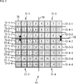
- unit pixel areas 71-1 to 71-4 that are unit pixel areas 51A of 2 (horizontal) ⁇ 2 (vertical) are arranged in the pixel area 51.
- the unit pixel area 71-1 is composed of pixel groups 72-1-1 to 72-1-4 consisting of 4 ⁇ 1 pixels 70. That is, the unit pixel area 71-1 is composed of 4 ⁇ 4 pixels 70.
- the unit pixel areas 71-2 to 71-4 also have pixel groups 72-2-1 to 72-2-4 and a pixel group 72- each composed of 4 ⁇ 1 pixels 70. 3-1 to 72-3-4 and pixel groups 72-4-1 to 72-4-4.
- unit pixel areas 71-1 to 71-4 are collectively referred to as a unit pixel area 71 when it is not necessary to distinguish them.
- pixel groups 72-1-1 to 72-1-4, pixel groups 72-2-1 to 72-2-4, pixel groups 72-3-1 to 72-3-4, and pixel group 72- 4-1 to 72-4-4 are collectively referred to as a pixel group 72.
- the pixel groups 72 constituting the unit pixel regions 71 adjacent in the vertical direction are alternately arranged in the vertical direction. Specifically, the pixel groups 72-1-1 to 72-1-4 in the unit pixel area 71-1 adjacent in the vertical direction and the pixel groups 72-2-1 to 72-72 in the unit pixel area 71-2. 2-4, in order from the top, the pixel group 72-1-1, the pixel group 72-2-1, the pixel group 72-1-2, the pixel group 72-2-2, the pixel group 72-1-3, The pixel group 72-2-3, the pixel group 72-1-4, and the pixel group 72-2-4 are arranged.
- Reference numeral 4 denotes a pixel group 72-3-1, a pixel group 72-4-1, a pixel group 72-3-2, a pixel group 72-4-2, a pixel group 72-3-3, and a pixel group 72 in order from the top. 4-3, a pixel group 72-3-4, and a pixel group 72-4-4.
- the reading order of each pixel 70 is set according to the following first to third conditions.
- the first condition is that the readout order of the pixels 70 adjacent to the boundary of every two rows of the pixels 70 among the boundaries of the unit pixel regions 71 adjacent in the vertical direction is line symmetric with respect to the boundary. is there.
- the second condition is that the order in which the pixels 70 of the two unit pixel areas 71 adjacent in the horizontal direction are read out is axisymmetric with respect to the boundary of the unit pixel area 71.
- the third condition is that the reading order of the pixels 70 constituting each pixel group 72 is continuous in the horizontal direction.
- the boundaries of every two rows among the boundaries 73-1 to 73-7 of the unit pixel area 71-1 (71-3) and the unit pixel area 71-2 (71-4) adjacent in the vertical direction are: They are a boundary 73-1, a boundary 73-3, a boundary 73-5, and a boundary 73-7. Therefore, for example, in accordance with the first to third conditions, the reading order of the pixel 70 immediately above the boundary 73-1 and the reading order of the pixel 70 immediately below the boundary 73-1 are 1, 2, 3, in order from the left. Set to 4, 4, 3, 2, 1.
- the reading order of the pixels 70 immediately above the boundary 73-1 and the reading order of the pixels 70 immediately below the boundary 73-1 are the same in order from the left, and are line symmetric with respect to the boundary 73-1.
- the readout order of each pixel 70 in the unit pixel area 71-1 (71-2) and the unit pixel area 71-3 (71-4) adjacent in the horizontal direction is the unit pixel area 71-1 (71-2).
- the reading order of the pixel group 72-1-1, the pixel group 72-3-1, the pixel group 72-2-1, and the pixels 70 arranged in the horizontal direction in the pixel group 72-4-1 is continuous. .
- the pixels 70 constituting the unit pixel region 71 adjacent in the vertical direction and having the same readout order are separated by the boundary 73-1, the boundary 73-3, the boundary 73-5, or the boundary 73- every two rows. 7 facing vertically. Therefore, by arranging the pixel drive line 52 in the vicinity of the boundary 73-1, the boundary 73-3, the boundary 73-5, or the boundary 73-7, the pixel drive line 52 between the pixels 70 can be shared. it can.
- the pixel drive line 52 can be shared.
- the pixel drive lines 52 are formed for every two rows by the number of horizontal pixels 70 constituting the unit pixel region 71 (4 in the example of FIG. 2).
- the reading order of the adjacent pixels 70 through the boundary 73-1, the boundary 73-3, the boundary 73-5, the boundary 73-7, and the boundary 74 is the same. Accordingly, it is possible to prevent image distortion at the boundary of the unit pixel region 71.
- FIG. 2 for convenience of explanation, only the pixel drive line 52 of the pixel 70 whose readout order is 5 is illustrated, but the pixel drive line 52 of the pixel 70 whose readout order is other than 5 is similarly formed. The This also applies to FIGS. 3, 4, 6, and 7 described later.
- FIG. 3 is a diagram illustrating a second configuration example of the pixel region 51 in FIG. 1.
- the configuration of the pixel region 51 in FIG. 3 is the same as that in FIG. 2 except that the pixel group constituting the unit pixel region 71 is 16 pixel groups each including 1 ⁇ 1 pixels 70 and the arrangement of the pixel groups.
- the configuration is the same.
- the unit pixel area 71-1 in FIG. 3 is composed of 16 pixel groups 91-1-1 to 91-1-16 consisting of 1 ⁇ 1 pixels 70.
- Each of the unit pixel areas 71-2 to 71-4 is composed of 16 pixel groups each composed of 1 ⁇ 1 pixels 70, similarly to the unit pixel area 71-1.
- the pixel groups of the unit pixel areas 71-1 to 71-4 are collectively referred to as a pixel group 91 when it is not necessary to distinguish them.
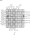
- the pixel groups 91 constituting the unit pixel regions 71 adjacent in the vertical direction are alternately arranged in the horizontal direction and the vertical direction. That is, the pixel groups 91 of the two unit pixel regions 71 adjacent in the vertical direction are arranged in a checkered pattern.
- the pixel groups 91 in the unit pixel area 71-1 and the pixel groups 91 in the unit pixel area 71-2 that are adjacent in the vertical direction are alternately arranged in the horizontal direction and the vertical direction.
- each pixel group 91 of the unit pixel area 71-3 adjacent in the vertical direction and each pixel group 91 of the unit pixel area 71-4 are alternately arranged in the horizontal direction and the vertical direction.
- the reading order of each pixel 70 is set in accordance with the above-described first to third conditions, similarly to the pixel area 51 of FIG. Thereby, the reading order of each pixel 70 in the pixel area 51 of FIG. 3 is the same as the reading order of each pixel 70 of the pixel area 51 of FIG.
- the pixel drive line 52 is arranged in the vicinity of the boundary 73-1, the boundary 73-3, the boundary 73-5, or the boundary 73-7, so that the unit pixel regions 71 that are adjacent in the vertical direction are read out. It is possible to share the pixel drive line 52 that controls the reading of the pixels 70 having the same. As a result, in the CMOS image sensor 50, the pixel drive lines 52 are formed for every two rows by the number of horizontal pixels 70 constituting the unit pixel region 71 (4 in the example of FIG. 3).
- FIG. 4 is a diagram illustrating a third configuration example of the pixel region 51 of FIG.
- the configuration of the pixel region 51 in FIG. 4 is the same as the configuration in FIG. 3 except that the pixel group constituting the unit pixel region 71 is four pixel groups including 2 ⁇ 2 pixels 70.
- the unit pixel area 71-1 in FIG. 4 is composed of pixel groups 111-1-1 to 111-1-4 made up of 2 ⁇ 2 pixels 70.
- the unit pixel areas 71-2 to 71-4 also have pixel groups 111-2-1 to 111-2-4 and pixel groups 111- each composed of 2 ⁇ 2 pixels 70, respectively. 3-1 to 111-3-4 and pixel groups 111-4-1 to 111-4-4.
- the pixel groups 111-1-1 to 111-1-4, the pixel groups 111-2-1 to 111-2-4, the pixel groups 111-3-1 to 111-3-4, and the pixel group When it is not necessary to distinguish 111-4-1 to 111-4-4, they are collectively referred to as a pixel group 111.
- the pixel groups 111 constituting the unit pixel regions 71 adjacent in the vertical direction are alternately arranged in the horizontal direction and the vertical direction, like the pixel groups 91 in FIG.
- the order of reading out each pixel 70 is set according to the above-described first to third conditions, similarly to the pixel region 51 of FIG.
- all the boundaries 112-1 to 112-3 of the unit pixel region 71 adjacent in the vertical direction exist every two rows. Accordingly, the readout order of each pixel 70 adjacent to all the boundaries 112-1 to 112-3 is line symmetric with respect to the boundaries 112-1 to 112-3.
- the reading order of the pixel 70 immediately above the boundary 112-1 and the reading order of the pixel 70 immediately below the boundary 112-1 are 3, 4, 5, 6, 6, 5, 4, 3 in order from the left. Is set.
- the reading order of the pixel 70 immediately above the boundary 112-1 and the reading order of the pixel 70 immediately below the boundary 112-1 are the same in order from the left, and are line symmetric with respect to the boundary 112-1.
- the reading order of each pixel 70 in the unit pixel area 71-2 (71-1) and the unit pixel area 71-3 (71-4) adjacent in the horizontal direction is the unit pixel area 71-2 (71-1).
- the pixels 70 constituting the unit pixel region 71 adjacent in the vertical direction and having the same readout order face each other in the vertical direction with respect to the boundaries 112-1 to 112-3 every two rows. Therefore, by arranging the pixel drive lines 52 in the vicinity of the boundaries 112-1 to 112-3, the pixel drive lines 52 of the pixels 70 can be shared. As a result, in the CMOS image sensor 50, the pixel drive lines 52 are formed for every two rows by the number of horizontal pixels 70 (4 in the example of FIG. 4) constituting the unit pixel region 71.
- the reading order of the adjacent pixels 70 through the boundaries 112-1 to 112-3 and the boundary 74 is the same. Accordingly, it is possible to prevent image distortion at the boundary of the unit pixel region 71.
- FIG. 5 is a diagram illustrating a fourth configuration example of the pixel region 51 in FIG. 1.
- the configuration of the pixel region 51 in FIG. 5 is the same as the configuration in FIG. 4 except that the unit pixel region 51A is configured from one pixel group 111 and the setting conditions for the order in which each pixel 70 is read.
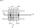
- unit pixel areas 131-1 to 131-4 that are 2 ⁇ 2 unit pixel areas 51A are arranged in the pixel area 51 of FIG.
- the unit pixel area 131-1 is composed of one pixel group 111-1-1. That is, the unit pixel region 131-1 is composed of 2 ⁇ 2 pixels 70.
- the unit pixel regions 131-2 to 131-4 are respectively formed by one pixel group 111-2-1, pixel group 111-3-1, and pixel group 111-4-1. Composed.
- the unit pixel regions 131-1 to 131-4 are collectively referred to as a unit pixel region 131 when it is not necessary to distinguish them.
- the reading order of each pixel 70 is set according to the first condition and the second condition described above. Therefore, for example, in accordance with the first and second conditions, the readout order of the pixel 70 immediately above the boundary 132 between the unit pixel region 131-1 and the unit pixel region 131-2 adjacent in the vertical direction and the pixel immediately below the boundary 132
- the reading order of 70 is set to 4, 2, 2, and 4 in order from the left.
- the reading order of the pixels 70 immediately above the boundary 132 and the reading order of the pixels 70 immediately below the boundary 132 are the same in order from the left, and are line symmetric with respect to the boundary 132. Further, the reading order of each pixel 70 in the unit pixel region 131-1 (131-2) and the unit pixel region 131-3 (131-4) adjacent in the horizontal direction is the unit pixel region 131-1 (131-2). Are the same in order from the boundary 133 side of the unit pixel region 131-3 (131-4), and are symmetrical with respect to the boundary 133.
- the pixels 70 constituting the unit pixel region 131 adjacent in the vertical direction and having the same readout order face each other in the vertical direction with respect to the boundary 132. Therefore, by arranging the pixel drive line 52 in the vicinity of the boundary 132, the pixel drive line 52 between the pixels 70 can be shared. As a result, in the CMOS image sensor 50, the pixel drive lines 52 are formed for every two rows by the number of horizontal pixels 70 constituting the unit pixel region 131 (2 in the example of FIG. 5).
- the reading order of the adjacent pixels 70 through the boundary 132 and the boundary 133 is the same. Accordingly, it is possible to prevent image distortion at the boundary of the unit pixel region 131.
- the setting condition of the order of reading out each pixel 70 in the pixel region 51 of FIG. 5 may include not only the first and second conditions but also the third condition.
- FIG. 6 is a diagram illustrating a fifth configuration example of the pixel region 51 of FIG.
- the configuration of the pixel region 51 in FIG. 6 is the same as the configuration in FIG. 4 except for the setting conditions for the order of reading out each pixel 70.
- the reading order of each pixel 70 is set according to the second and third conditions described above and the new fourth condition.
- the fourth condition is that the order of reading the adjacent pixels 70 across the boundaries 112-1 to 112-3 of every two rows of the pixels 70 in the boundaries of the unit pixel regions 71 adjacent in the vertical direction is the boundary 112 -1 to 112-3 are non-linearly symmetric but are the same for each unit pixel region 71.
- the reading order of the pixel 70 immediately above the boundary 112-1 is set to 3, 4, 6, 5, 5, 6, 4, 3 in order from the left.
- the reading order of the pixels 70 immediately below the boundary 112-1 is set to 4, 3, 5, 6, 6, 5, 3, 4 in order from the left.
- the order of reading out the pixels 70 immediately above the boundary 112-1 and the order of reading out the pixels 70 immediately below the boundary 112-1 are not the same in order from the left, and are axisymmetric with respect to the boundary 112-1. .
- the reading order of the two pixels 70 in the pixel area 71-2 (71-3) is 3 and 4 for both.
- the reading order of the two pixels 70 in the unit pixel area 71-1 (71-4) is 5 and 6 for both.
- each pixel 70 in the unit pixel area 71-2 (71-1) and the unit pixel area 71-3 (71-4) adjacent in the horizontal direction is the unit pixel area 71-2 (71-1).
- the boundary 74 of the unit pixel region 71-3 (71-4) are symmetrical with respect to the boundary 74.
- the pixels 70 constituting the unit pixel regions 71 adjacent in the vertical direction and having the same reading order are adjacent to the same boundaries 112-1 to 112-3 every two rows. Therefore, by arranging the pixel drive lines 52 in the vicinity of the boundaries 112-1 to 112-3, the pixel drive lines 52 of the pixels 70 can be shared. As a result, in the CMOS image sensor 50, the pixel drive lines 52 are formed for every two rows by the number of horizontal pixels 70 constituting the unit pixel region 71 (4 in the example of FIG. 6).
- FIG. 7 is a diagram illustrating a sixth configuration example of the pixel region 51 of FIG.
- the configuration of the pixel area 51 in FIG. 7 is the same as the configuration in FIG.
- the order of reading out each pixel 70 is set according to the above-described fourth condition and new fifth condition.
- the fifth condition is that the reading order of each pixel 70 in two unit pixel areas 71 adjacent in the horizontal direction is axisymmetric with respect to the boundary 74 of the unit pixel area 71, but is adjacent to the boundary 74.
- the reading order of the pixels 70 to be read is the same for each unit pixel region 71.
- the reading order of the pixel 70 immediately above the boundary 73-3 is set to 5, 6, 7, 8, 8, 5, 6, 7 in order from the left.
- the reading order of the pixels 70 immediately below the boundary 73-3 is set to 7, 8, 5, 6, 6, 7, 8, and 5 in order from the left.
- the reading order of the pixels 70 immediately above the boundary 73-3 and the reading order of the pixels 70 immediately below the boundary 73-3 are not the same in order from the left, and are axisymmetric with respect to the boundary 73-1. .
- the order of reading out the four pixels 70 in the unit pixel area 71-1 (71-3) of the pixels 70 immediately above the boundary 73-3 and the unit pixels of the pixels 70 immediately below the boundary 73-3 are read.
- the reading order of the four pixels 70 in the area 71-2 (71-4) is both 5 to 8.
- the readout order of each pixel 70 in the unit pixel area 71-1 (71-2) and the unit pixel area 71-3 (71-4) adjacent in the horizontal direction is the unit pixel area 71-1 (71-2).
- the reading order of the four pixels 70 in -4) is both 5 to 8.
- the reading order of the pixels 70 arranged in the horizontal direction in the pixel group 72-1-2, the pixel group 72-2-2, the pixel group 72-3-2, and the pixel group 72-4-2 is not continuous. .
- the pixels 70 constituting the unit pixel regions 71 adjacent in the vertical direction and having the same readout order are separated from each other by the same boundaries 73-1, 73-3, 73-5, or 73-7. Adjacent to. Therefore, by arranging the pixel drive line 52 in the vicinity of the boundaries 73-1, 73-3, 73-5, or 73-7, the pixel drive line 52 between the pixels 70 can be shared. As a result, in the CMOS image sensor 50, the pixel drive lines 52 are formed for every two rows by the number of horizontal pixels 70 constituting the unit pixel region 71 (4 in the example of FIG. 7).
- the square represents the pixel 70, and the number in the square represents the readout order set for the pixel 70.
- the diagonal lines, polka dots, vertical stripes, and grids attached to the squares indicate that the color filter color of the pixel 70 represented by the square is red (R), green (Gr), green (Gb), and blue (B). It represents that.
- the color filter array of the pixels 70 arranged in the pixel region 51 is a Bayer array.
- the color of the color filter of the pixel 70 is R, Gr, Gb, and B in the order of upper left, upper right, lower left, and lower right for each 2 (horizontal) ⁇ 2 (vertical) pixel 70.
- the color filter color of the pixel 70 that constitutes each of the unit pixel areas 131 in the pixel area 51 and that has the same reading order includes the color filter color of the pixel 70. All of R, Gr, Gb, and B that can be assigned as colors are included.
- the signal processing unit 62 performs interpolation based on the R, Gr, Gb, or B pixel signal of each pixel 70 obtained in this way, thereby performing R, Gr, Gb, and B pixels of all the pixels 70.
- the signal is generated as an image.
- the image contains white light white and no color artifacts occur.
- a pixel area 150 in which the color of the color filter of the pixel 70 having the same reading order in each unit pixel area 131 is the same is provided. If the pixel 70 is irradiated with white light by flash or the like during reading of the pixel 70 whose reading order is 2, the color artifact is generated.
- the pixel 70 when the pixel 70 is irradiated with white light by flash or the like during the reading of the pixel signal of the pixel 70 whose reading order is 2, in the pixel 70 whose reading order is 3 or later. Only the Gb and B pixel signals of the white light are acquired. As a result, the image generated by the signal processing unit 62 includes only Gb and B of white corresponding to white light. Thus, color artifacts occur.
- the image includes white corresponding to the white light, and the color artifact is Does not occur.
- a pixel signal having a predetermined threshold value or more may be generated in a pattern shape due to white corresponding to white light.
- the signal processing unit 62 uses the flash light to determine the predetermined threshold. It is determined that the above pixel signal is generated in a pattern. Then, the signal processing unit 62 corrects a pixel signal that is equal to or greater than a predetermined threshold using the pixel signal stored in the memory unit 63. Examples of the correction method include the following first method and second method.
- the first method is for a pixel 70 whose pixel signal is equal to or greater than a predetermined threshold, with respect to at least one predetermined threshold before and after the pixel signal that is equal to or greater than the predetermined threshold.
- a small pixel signal is used to correct a pixel signal that is equal to or greater than the predetermined threshold.
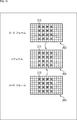
- a pixel signal 211 that is equal to or greater than a predetermined threshold value of the image 201 of the nth frame is a predetermined threshold value in the image 202 of the n ⁇ 1th frame of the pixel 70 corresponding to the pixel signal 211.
- Correction is performed using a smaller pixel signal 212 and a pixel signal 213 smaller than a predetermined threshold in the image 203 of the (n + 1) th frame.
- the square represents the pixel signal of each pixel 70. The same applies to FIG. 11 described later.
- the correction by the first method can be performed when the image captured by the CMOS image sensor 50 is a moving image.
- the corrected resolution can be the same as the resolution before the correction.
- the second method uses a pixel signal that is equal to or greater than a predetermined threshold by using a pixel signal that is smaller than the predetermined threshold of the pixels 70 around the pixel 70 corresponding to the pixel signal that is equal to or greater than the predetermined threshold.
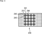
- a method of correcting the above That is, in the second method, a pixel signal 231 that is equal to or larger than a predetermined threshold in the image 230 is smaller than a predetermined threshold of the pixels 70 around the pixel 70 corresponding to the pixel signal 231 (example in FIG. 11). Then, the correction is performed using the pixel signals 241 to 244) of the upper, lower, left, and right pixels 70.
- the correction by the second method can be performed regardless of whether the image captured by the CMOS image sensor 50 is a moving image or a still image.
- the resolution after correction is lower than the resolution before correction.
- the pixel drive lines 52 of the pixels 70 that constitute the unit pixel areas 71 (131) adjacent in the vertical direction and that have the same readout order are shared. Therefore, the number of pixel drive lines 52 can be reduced as compared with the case where the pixel drive line 52 is formed for each pixel 70.
- the unit pixel area 71 (131) is composed of H (horizontal) ⁇ V (vertical) pixels
- the number of pixel drive lines 52 required for one unit pixel area 71 (131) is HxV / 2.
- the number of pixel drive lines 52 per row of the pixels 70 is H / 2.
- FIG. 12 is a diagram showing an arrangement example of each part of the CMOS image sensor 50 of FIG.
- the CMOS image sensor 50 is formed by stacking a semiconductor substrate 264 (first chip) and a semiconductor substrate 265 (second chip).
- a pixel region 51 is formed on the semiconductor substrate 264, and a control circuit 271 and a logic circuit 272 are formed on the semiconductor substrate 265.
- the semiconductor substrate 264 and the semiconductor substrate 265 are connected for each unit pixel region 71 (131).
- the control circuit 271 is a circuit including a pixel driving unit 54, a reading region 55, a reading driving line 56, a vertical signal line 57, a reading circuit driving unit 58, a column processing unit 59, a horizontal driving unit 60, and a system control unit 61.
- the logic circuit 272 is a circuit including the signal processing unit 62 and the memory unit 63.
- control circuit 271 and the logic circuit 272 are formed on the same semiconductor substrate 265, but may be formed on different semiconductor substrates.
- FIG. 13 is a block diagram illustrating a configuration example of an embodiment of an imaging apparatus as an electronic apparatus to which the present disclosure is applied.
- the imaging apparatus 1000 includes a lens group 1001, a solid-state imaging device 1002, a DSP circuit 1003, a frame memory 1004, a display unit 1005, a recording unit 1006, an operation unit 1007, and a power supply unit 1008.
- the DSP circuit 1003, the frame memory 1004, the display unit 1005, the recording unit 1006, the operation unit 1007, and the power supply unit 1008 are connected to each other via a bus line 1009.
- the lens group 1001 takes in incident light (image light) from a subject and forms an image on the imaging surface of the solid-state imaging device 1002.
- the solid-state image sensor 1002 includes the above-described CMOS image sensor 50.
- the solid-state imaging device 1002 converts the amount of incident light imaged on the imaging surface by the lens group 1001 into an electrical signal in units of pixels and supplies the electrical signal to the DSP circuit 1003 as a pixel signal.
- the DSP circuit 1003 performs predetermined image processing on the pixel signal supplied from the solid-state imaging device 1002, supplies the image signal after the image processing to the frame memory 1004 in units of frames, and temporarily stores them.
- the display unit 1005 includes, for example, a panel type display device such as a liquid crystal panel or an organic EL (Electro Luminescence) panel, and displays an image based on a pixel signal in a frame unit temporarily stored in the frame memory 1004.
- a panel type display device such as a liquid crystal panel or an organic EL (Electro Luminescence) panel, and displays an image based on a pixel signal in a frame unit temporarily stored in the frame memory 1004.
- the recording unit 1006 includes a DVD (Digital Versatile Disk), a flash memory, and the like, and reads and records pixel signals in units of frames temporarily stored in the frame memory 1004.
- DVD Digital Versatile Disk
- flash memory and the like, and reads and records pixel signals in units of frames temporarily stored in the frame memory 1004.
- the operation unit 1007 issues operation commands for various functions of the imaging apparatus 1000 under operation by the user.
- the power supply unit 1008 appropriately supplies power to the DSP circuit 1003, the frame memory 1004, the display unit 1005, the recording unit 1006, and the operation unit 1007.
- the electronic apparatus to which the present technology is applied may be any device that uses the CMOS image sensor 50 for the image capturing unit (photoelectric conversion unit).
- the mobile terminal device having the imaging function, and the image reading unit may have a CMOS. There are copying machines using the image sensor 50.
- FIG. 14 is a diagram illustrating a usage example in which the above-described CMOS image sensor 50 is used.
- CMOS image sensor 50 can be used in various cases for sensing light such as visible light, infrared light, ultraviolet light, and X-ray as follows.
- Devices for taking images for viewing such as digital cameras and mobile devices with camera functions
- Devices used for traffic such as in-vehicle sensors that capture the back, surroundings, and interiors of vehicles, surveillance cameras that monitor traveling vehicles and roads, and ranging sensors that measure distances between vehicles, etc.
- Equipment used for home appliances such as TVs, refrigerators, air conditioners, etc. to take pictures and operate the equipment according to the gestures ⁇ Endoscopes, equipment that performs blood vessel photography by receiving infrared light, etc.
- Equipment used for medical and health care ⁇ Security equipment such as security surveillance cameras and personal authentication cameras ⁇ Skin measuring instrument for photographing skin and scalp photography Such as a microscope to do beauty Equipment used for sports-Equipment used for sports such as action cameras and wearable cameras for sports applications-Used for agriculture such as cameras for monitoring the condition of fields and crops apparatus
- the number of pixel groups constituting the unit pixel region 51A is 1 or more, the number can be arbitrarily set. Further, the number of pixels constituting the pixel group can be any number as long as it is 1 or more. Furthermore, the number of unit pixel areas 51A constituting the pixel area 51 can be any number as long as it is two or more.
- this indication can also take the following structures.
- a unit pixel area composed of a plurality of pixels arranged in an array; and A readout circuit that is provided for each unit pixel region, and reads out pixel signals of the plurality of pixels constituting the unit pixel region in a predetermined order; and A solid-state imaging device configured to share wiring for controlling reading of the pixels having the same reading order, which constitutes the unit pixel region adjacent in a predetermined direction.
- the solid-state imaging device according to (1) wherein the plurality of pixels are configured to be one or more pixel groups including pixels in one or two rows.
- each pixel group constituting the unit pixel region adjacent in the predetermined direction is arranged alternately.
- the readout order of the pixels adjacent to the boundary of every two rows of the pixels is configured to be the same for each unit pixel area.
- the readout order of the pixels adjacent to the boundary of every two rows of the pixels is configured to be line symmetric with respect to the boundary.
- the color of the color filter included in the pixels having the same readout order in all the unit pixel areas is configured to include all colors that can be assigned as the color of the color filter.
- the solid-state image sensor as described in any one of thru
- the solid-state imaging device further including: a correction unit that corrects the pixel signal when the pixel signal is equal to or greater than a predetermined threshold.
- the correction unit corrects a pixel signal that is equal to or higher than the predetermined threshold when a ratio of the pixels whose pixel signal is equal to or higher than the predetermined threshold with respect to all the pixels in a predetermined region is equal to or higher than the threshold.
- the solid-state imaging device configured as described above.
- the correction unit uses at least one pixel signal temporally before and after the pixel signal of the pixel corresponding to the pixel signal that is equal to or greater than the predetermined threshold, and a pixel signal that is equal to or greater than the predetermined threshold.
- the solid-state imaging device configured to correct (10)
- the correction unit is configured to correct a pixel signal that is equal to or greater than the predetermined threshold by using the pixel signal of the pixel around the pixel that corresponds to the pixel signal that is equal to or greater than the predetermined threshold.
- the solid-state image sensor as described in. (11)
- the unit pixel region is formed in a first chip;
- the readout circuit is formed in a second chip;
- the solid-state imaging device according to any one of (1) to (10), wherein the first chip and the second chip are configured to be connected for each unit pixel region.
- a unit pixel area composed of a plurality of pixels arranged in an array; and A readout circuit that is provided for each unit pixel region, and reads out pixel signals of the plurality of pixels constituting the unit pixel region in a predetermined order; and
- An electronic apparatus comprising: a solid-state imaging device configured to share a wiring for controlling reading of the pixels having the same reading order, which constitutes the unit pixel region adjacent in a predetermined direction.
- CMOS image sensor 52 pixel drive line, 55A readout circuit, 62 signal processing unit, 70 pixels, 71-1 to 71-4 unit pixel area, 72-1-1 to 72-1-4, 72-2-1 To 72-2-4, 72-3-1 to 72-3-4, 72-4-1 to 72-4-4, pixel group, 73-1 to 73-7 boundary, 91-1-1 to 91- 1-16 pixel group, 111-1-1 to 111-1-4, 111-2-1 to 111-2-4, 111-3-1 to 111-3-4, 111-4-1 to 111- 4-4 pixel group, 131-1 to 131-4 unit pixel area, 211 to 213 pixel signal, 231, 241 to 244 pixel signal, 264, 265 semiconductor substrate, 1000 imaging device, 1002 solid-state imaging device
Landscapes
- Engineering & Computer Science (AREA)
- Multimedia (AREA)
- Signal Processing (AREA)
- Transforming Light Signals Into Electric Signals (AREA)
- Solid State Image Pick-Up Elements (AREA)
Abstract
本開示は、単位画素領域ごとに各画素の画素信号を所定の順番で読み出す場合に、読み出しを制御する配線の本数を削減することができるようにする固体撮像素子および電子機器に関する。 単位画素領域は、アレイ状に配置された、複数の画素から構成される。読み出し回路は、単位画素領域ごとに設けられ、単位画素領域を構成する複数の画素の画素信号を所定の順番で読み出す。垂直方向に隣接する単位画素領域を構成する、読み出す順番が同一である画素どうしの読み出しを制御する画素駆動線は共有される。本開示は、例えば、CMOSイメージセンサ等に適用することができる。
Description
本開示は、固体撮像素子および電子機器に関し、特に、単位画素領域ごとに各画素の画素信号を所定の順番で読み出す場合に、読み出しを制御する配線の本数を削減することができるようにした固体撮像素子および電子機器に関する。
近年、裏面照射型撮像チップと信号処理チップとが積層された撮像素子がある。このような撮像素子において、裏面照射型撮像チップに形成されるアレイ状に配置された画素を、複数の画素からなる単位画素領域に分割し、単位画素領域ごとに各画素の画素信号を所定の順番で読み出すことが考案されている(例えば、特許文献1参照)。
特許文献1の発明は、隣接する単位画素領域内の画素信号を読み出す順番が同一である画素どうしの位置が、その単位画素領域の境界に対して線対称になるように、画素信号の読み出しを制御することにより、単位画素領域の境界における画像の歪みを抑制している。
ところで、特許文献1の発明では、単位画素領域内の各画素に対して、画素信号の読み出しを制御する配線(以下、画素駆動線という)が設けられている。従って、単位画素領域がH(横)×V(縦)(H,Vは自然数)の画素から構成される場合、1つの単位画素領域に必要な画素駆動線はH×V本であり、画素の各行に対して形成される画素駆動線の本数はH本である。よって、単位画素領域内の画素の数の増加に伴い、画素駆動線の本数が増加する。
本開示は、このような状況に鑑みてなされたものであり、単位画素領域ごとに各画素の画素信号を所定の順番で読み出す場合に、読み出しを制御する配線の本数を削減することができるようにするものである。
本開示の第1の側面の固体撮像素子は、アレイ状に配置された、複数の画素から構成される単位画素領域と、前記単位画素領域ごとに設けられた、前記単位画素領域を構成する前記複数の画素の画素信号を所定の順番で読み出す読み出し回路とを備え、所定の方向に隣接する前記単位画素領域を構成する、読み出す順番が同一である前記画素どうしの読み出しを制御する配線は共有されるように構成された固体撮像素子である。
本開示の第1の側面においては、アレイ状に配置された、複数の画素から構成される単位画素領域と、前記単位画素領域ごとに設けられた、前記単位画素領域を構成する前記複数の画素の画素信号を所定の順番で読み出す読み出し回路とが備えられ、所定の方向に隣接する前記単位画素領域を構成する、読み出す順番が同一である前記画素どうしの読み出しを制御する配線が共有される。
本開示の第2の側面の電子機器は、アレイ状に配置された、複数の画素から構成される単位画素領域と、前記単位画素領域ごとに設けられた、前記単位画素領域を構成する前記複数の画素の画素信号を所定の順番で読み出す読み出し回路とを備え、所定の方向に隣接する前記単位画素領域を構成する、読み出す順番が同一である前記画素どうしの読み出しを制御する配線は共有されるように構成された固体撮像素子を備える電子機器である。
本開示の第2の側面においては、アレイ状に配置された、複数の画素から構成される単位画素領域と、前記単位画素領域ごとに設けられた、前記単位画素領域を構成する前記複数の画素の画素信号を所定の順番で読み出す読み出し回路とが備えられ、所定の方向に隣接する前記単位画素領域を構成する、読み出す順番が同一である前記画素どうしの読み出しを制御する配線が共有される。
本開示の第1および第2の側面によれば、撮像することができる。また、本開示の第1の側面によれば、単位画素領域ごとに各画素の画素信号を所定の順番で読み出す場合に、読み出しを制御する配線の本数を削減することができる。
なお、ここに記載された効果は必ずしも限定されるものではなく、本開示中に記載されたいずれかの効果であってもよい。
以下、本開示を実施するための形態(以下、実施の形態という)について説明する。なお、説明は以下の順序で行う。
1.第1実施の形態:CMOSイメージセンサ(図1乃至図12)
2.第2実施の形態:撮像装置(図13)
3.CMOSイメージセンサの使用例(図14)
1.第1実施の形態:CMOSイメージセンサ(図1乃至図12)
2.第2実施の形態:撮像装置(図13)
3.CMOSイメージセンサの使用例(図14)
<第1実施の形態>
(CMOSイメージセンサの一実施の形態の構成例)
図1は、本開示を適用した固体撮像素子としてのCMOSイメージセンサの一実施の形態の構成例を示す図である。
(CMOSイメージセンサの一実施の形態の構成例)
図1は、本開示を適用した固体撮像素子としてのCMOSイメージセンサの一実施の形態の構成例を示す図である。
CMOSイメージセンサ50は、画素領域51、画素駆動線52、画素駆動部54、読み出し領域55、読み出し駆動線56、垂直信号線57、読み出し回路駆動部58、カラム処理部59、水平駆動部60、システム制御部61、信号処理部62、およびメモリ部63が、図示せぬシリコン基板等の半導体基板(チップ)に形成されたものである。
CMOSイメージセンサ50の画素領域51には、入射光の光量に応じた電荷量の電荷を発生して内部に蓄積する光電変換素子を有する複数の画素が、アレイ状に2次元配置される。画素領域51に配置された画素は、複数の画素ごとに、単位画素領域51Aに分割される。即ち、画素領域51は、アレイ状に配置された、複数の画素から構成される単位画素領域51Aにより構成される。各画素には、その画素を含む単位画素領域51Aごとに、単位画素領域51A内の各画素の光電変換素子に蓄積された電荷に対応する画素信号が所定の順番で読み出されるように、その画素の画素信号を読み出す順番が設定されている。
画素領域51には、画素に対して、2行ごとに、単位画素領域51A内の水平方向の画素数(列数)だけ画素駆動線52が形成される。画素駆動線52は、対応する2行の画素のうちの読み出す順番が同一である画素ごとに接続され、画素信号の読み出しを制御する。
画素駆動部54は、シフトレジスタやアドレスデコーダなどによって構成される。画素駆動部54は、読み出す順番にしたがって、その読み出す順番の画素に接続された画素駆動線52に信号を供給する。これにより、各単位画素領域51A内の画素の画素信号は、その画素に設定された読み出す順番で、同一の読み出す順番が設定された他の単位画素領域51A内の画素の画素信号と同時に読み出される。読み出された画素信号は、読み出し領域55のうちの、その画素信号に対応する単位画素領域51Aの読み出し回路55Aに出力される。
読み出し領域55には、各単位画素領域51Aの読み出し回路55Aがアレイ状に2次元配置される。読み出し回路55Aは、対応する単位画素領域51A内の画素から出力された画素信号に対して、A/D変換処理、CDS(Correlated Double Sampling)(相関二重サンプリング)処理等の信号処理を行い、一時的に保持する。また、読み出し領域55には、アレイ状の読み出し回路55Aに対して、行ごとに読み出し駆動線56が形成され、列ごとに垂直信号線57が形成される。
読み出し回路駆動部58は、シフトレジスタやアドレスデコーダなどによって構成され、読み出し領域55の各読み出し回路55Aを行単位等で駆動する。具体的には、読み出し回路駆動部58は、各行を順に選択し、選択行の読み出し駆動線56に選択信号を出力する。これにより、選択行の各読み出し回路55Aに保持された信号処理後の画素信号が読み出され、垂直信号線57に供給される。
カラム処理部59は、読み出し回路55Aの列ごとに信号処理回路を有する。カラム処理部59の各信号処理回路は、選択行の各読み出し回路55Aから垂直信号線57を通して出力される画素信号を一時的に保持する。
水平駆動部60は、シフトレジスタやアドレスデコーダなどによって構成され、カラム処理部59の信号処理回路を順番に選択する。この水平駆動部60による選択走査により、カラム処理部59の各信号処理回路に保持された画素信号が順番に信号処理部62に出力される。
システム制御部61は、各種のタイミング信号を生成するタイミングジェネレータ等によって構成され、タイミングジェネレータで生成された各種のタイミング信号を基に画素駆動部54、読み出し回路駆動部58、カラム処理部59、および水平駆動部60を制御する。
信号処理部62は、カラム処理部59から出力される画素信号をフレーム単位で画像としてメモリ部63に格納する。信号処理部62は、メモリ部63に格納されている画像の各画素の画素信号が、所定の閾値以上であるかどうかを判定する。
信号処理部62は、画素領域51内の所定の領域における、全ての画素に対する画素信号が所定の閾値以上である画素の割合が閾値以上である場合、メモリ部63に格納されている画素信号を用いて、所定の閾値以上である画素信号を補正する。信号処理部62は、所定の閾値以上である画素信号が補正された画像を出力する。一方、画素領域51内の所定の領域における、全ての画素に対する画素信号が所定の閾値以上である画素の割合が閾値より小さい場合、信号処理部62は、メモリ部63に格納されている画像をそのまま出力する。
メモリ部63は、DRAM(Dynamic Random Access Memory)やSRAM(Static Random Access Memory)などにより構成される。
(画素領域の第1の構成例)
図2は、図1の画素領域51の第1の構成例を示す図である。
図2は、図1の画素領域51の第1の構成例を示す図である。
なお、図2において、正方形は、画素70を表し、正方形内の数字は、その画素70に設定された読み出す順番を表している。また、同一の単位画素領域51A内の画素70を表す正方形には、同一のハッチが付されている。これらのことは、後述する図3乃至7においても同様である。
図2の例では、画素領域51に、2(横)×2(縦)の単位画素領域51Aである単位画素領域71-1乃至71-4が配置される。単位画素領域71-1は、4×1の画素70からなる画素群72-1-1乃至72-1-4から構成される。即ち、単位画素領域71-1は、4×4の画素70から構成される。
単位画素領域71-2乃至71-4も、単位画素領域71-1と同様に、それぞれ、4×1の画素70からなる画素群72-2-1乃至72-2-4、画素群72-3-1乃至72-3-4、画素群72-4-1乃至72-4-4により構成される。
なお、以下では、単位画素領域71-1乃至71-4を特に区別する必要がない場合、それらをまとめて単位画素領域71という。同様に、画素群72-1-1乃至72-1-4、画素群72-2-1乃至72-2-4、画素群72-3-1乃至72-3-4、および画素群72-4-1乃至72-4-4をまとめて、画素群72という。
垂直方向に隣接する単位画素領域71を構成する各画素群72は、垂直方向に交互に配置される。具体的には、垂直方向に隣接する単位画素領域71-1の各画素群72-1-1乃至72-1-4と、単位画素領域71-2の各画素群72-2-1乃至72-2-4は、先頭から順に、画素群72-1-1、画素群72-2-1、画素群72-1-2、画素群72-2-2、画素群72-1-3、画素群72-2-3、画素群72-1-4、画素群72-2-4となるように配置される。
また、垂直方向に隣接する単位画素領域71-3の各画素群72-3-1乃至72-3-4と、単位画素領域71-4の各画素群72-4-1乃至72-4-4は、先頭から順に、画素群72-3-1、画素群72-4-1、画素群72-3-2、画素群72-4-2、画素群72-3-3、画素群72-4-3、画素群72-3-4、画素群72-4-4となるように配置される。
各画素70の読み出す順番は、以下の第1乃至第3の条件にしたがって設定される。第1の条件は、垂直方向に隣接する単位画素領域71の境界のうちの画素70の2行ごとの境界に隣接する画素70の読み出す順番は、その境界に対して線対称であるという条件である。
第2の条件は、水平方向に隣接する2つの単位画素領域71の各画素70の読み出す順番は、単位画素領域71の境界に対して線対称であるという条件である。第3の条件は、各画素群72を構成する画素70の読み出す順番は、水平方向に連続するという条件である。
ここで、垂直方向に隣接する単位画素領域71-1(71-3)と単位画素領域71-2(71-4)の境界73-1乃至73-7のうちの2行ごとの境界は、境界73-1、境界73-3、境界73-5、境界73-7である。従って、例えば、第1乃至第3の条件にしたがって、境界73-1の直上の画素70の読み出す順番と境界73-1の直下の画素70の読み出す順番は、左から順に1,2,3,4,4,3,2,1に設定される。
即ち、境界73-1の直上の画素70の読み出す順番と境界73-1の直下の画素70の読み出す順番は、左から順に同一であり、境界73-1に対して線対称になっている。また、水平方向に隣接する単位画素領域71-1(71-2)と単位画素領域71-3(71-4)の各画素70の読み出す順番は、単位画素領域71-1(71-2)と単位画素領域71-3(71-4)の境界74側から順に同一であり、境界74に対して線対称になっている。さらに、画素群72-1-1、画素群72-3-1、画素群72-2-1、および画素群72-4-1内の水平方向に並ぶ画素70の読み出す順番は連続している。
以上により、垂直方向に隣接する単位画素領域71を構成する、読み出す順番が同一である画素70どうしは、2行ごとの境界73-1、境界73-3、境界73-5、または境界73-7に対して垂直方向に向き合う。従って、画素駆動線52を、境界73-1、境界73-3、境界73-5、または境界73-7付近に配置することで、この画素70どうしの画素駆動線52を共有化することができる。
例えば、垂直方向に隣接する単位画素領域71-1と単位画素領域71-2、および、単位画素領域71-3と単位画素領域71-4を構成する、読み出す順番が5である画素70どうしの画素駆動線52は共有化することができる。その結果、CMOSイメージセンサ50では、2行ごとに、単位画素領域71を構成する水平方向の画素70の数(図2の例では4)だけ画素駆動線52が形成される。
また、境界73-1、境界73-3、境界73-5、および境界73-7、並びに、境界74を介して隣り合う画素70の読み出す順番が同一になる。従って、単位画素領域71の境界における画像の歪みの発生を防止することができる。
なお、図2では、説明の便宜上、読み出す順番が5である画素70の画素駆動線52についてのみ図示してあるが、読み出す順番が5以外である画素70の画素駆動線52も同様に形成される。このことは、後述する図3、図4、図6、および図7においても同様である。
(画素領域の第2の構成例)
図3は、図1の画素領域51の第2の構成例を示す図である。
図3は、図1の画素領域51の第2の構成例を示す図である。
図3に示す構成のうち、図2の構成と同じ構成には同じ符号を付してある。重複する説明については適宜省略する。
図3の画素領域51の構成は、単位画素領域71を構成する画素群が1×1の画素70からなる16個の画素群である点、および、画素群の配置を除いて、図2の構成と同一である。
具体的には、図3の単位画素領域71-1は、1×1の画素70からなる16個の画素群91-1-1乃至91-1―16から構成される。単位画素領域71-2乃至71-4も、単位画素領域71-1と同様に、それぞれ、1×1の画素70からなる16個の画素群により構成される。なお、以下では、単位画素領域71-1乃至71-4の画素群を特に区別する必要がない場合、それらをまとめて画素群91という。
垂直方向に隣接する単位画素領域71を構成する各画素群91は、水平方向および垂直方向に交互に配置される。即ち、垂直方向に隣接する2つの単位画素領域71の各画素群91は、市松模様状に配置される。
具体的には、垂直方向に隣接する単位画素領域71-1の各画素群91と単位画素領域71-2の各画素群91は、水平方向および垂直方向に交互に配置される。また、垂直方向に隣接する単位画素領域71-3の各画素群91と、単位画素領域71-4の各画素群91は、水平方向および垂直方向に交互に配置される。
図3の画素領域51においても、図2の画素領域51と同様に、上述した第1乃至第3の条件にしたがって、各画素70の読み出す順番が設定される。これにより、図3の画素領域51の各画素70の読み出す順番は、図2の画素領域51の各画素70の読み出す順番と同一になる。
従って、画素駆動線52を、境界73-1、境界73-3、境界73-5、または境界73-7付近に配置することで、垂直方向に隣接する単位画素領域71を構成する、読み出す順番が同一である画素70どうしの読み出しを制御する画素駆動線52を共有化することができる。その結果、CMOSイメージセンサ50では、2行ごとに、単位画素領域71を構成する水平方向の画素70の数(図3の例では4)だけ画素駆動線52が形成される。
また、境界73-1、境界73-3、境界73-5、および境界73-7、並びに、境界74を介して隣り合う画素70の読み出す順番が同一になるので、単位画素領域71の境界における画像の歪みの発生を防止することができる。
(画素領域の第3の構成例)
図4は、図1の画素領域51の第3の構成例を示す図である。
図4は、図1の画素領域51の第3の構成例を示す図である。
図4に示す構成のうち、図3の構成と同じ構成には同じ符号を付してある。重複する説明については適宜省略する。
図4の画素領域51の構成は、単位画素領域71を構成する画素群が2×2の画素70からなる4個の画素群である点を除いて、図3の構成と同一である。
具体的には、図4の単位画素領域71-1は、2×2の画素70からなる画素群111-1-1乃至111-1-4から構成される。単位画素領域71-2乃至71-4も、単位画素領域71-1と同様に、それぞれ、2×2の画素70からなる画素群111-2-1乃至111-2-4、画素群111-3-1乃至111-3-4、画素群111-4-1乃至111-4-4により構成される。
なお、以下では、画素群111-1-1乃至111-1-4、画素群111-2-1乃至111-2-4、画素群111-3-1乃至111-3-4、および画素群111-4-1乃至111-4-4を特に区別する必要がない場合、それらをまとめて、画素群111という。
垂直方向に隣接する単位画素領域71を構成する各画素群111は、図3の各画素群91と同様に、水平方向および垂直方向に交互に配置される。
また、図4の画素領域51においても、図3の画素領域51と同様に、上述した第1乃至第3の条件にしたがって、各画素70の読み出す順番が設定される。なお、図4の例では、垂直方向に隣接する単位画素領域71の全ての境界112-1乃至112-3は2行ごとに存在する。従って、全ての境界112-1乃至112-3に隣接する各画素70の読み出す順番が、その境界112-1乃至112-3に対して線対称になる。
よって、例えば、境界112-1の直上の画素70の読み出す順番と境界112-1の直下の画素70の読み出す順番は、左から順に3,4,5,6,6,5,4,3に設定される。
即ち、境界112-1の直上の画素70の読み出す順番と境界112-1の直下の画素70の読み出す順番は、左から順に同一であり、境界112-1に対して線対称になっている。また、水平方向に隣接する単位画素領域71-2(71-1)と単位画素領域71-3(71-4)の各画素70の読み出す順番は、単位画素領域71-2(71-1)と単位画素領域71-3(71-4)の境界74側から順に同一であり、境界74に対して線対称になっている。
さらに、画素群111-1-1、画素群111-2-1、画素群111-3-1、画素群111-4-1、画素群111-2-2、画素群111-1-2、画素群111-4-2、および画素群111-3-2内の水平方向に並ぶ画素70の読み出す順番は連続している。
以上により、垂直方向に隣接する単位画素領域71を構成する、読み出す順番が同一である画素70どうしは、2行ごとの境界112-1乃至112-3に対して垂直方向に向き合う。従って、画素駆動線52を、境界112-1乃至112-3付近に配置することで、この画素70どうしの画素駆動線52を共有化することができる。その結果、CMOSイメージセンサ50では、2行ごとに、単位画素領域71を構成する水平方向の画素70の数(図4の例では4)だけ画素駆動線52が形成される。
また、境界112-1乃至112-3、並びに、境界74を介して隣り合う画素70の読み出す順番が同一になる。従って、単位画素領域71の境界における画像の歪みの発生を防止することができる。
(画素領域の第4の構成例)
図5は、図1の画素領域51の第4の構成例を示す図である。
図5は、図1の画素領域51の第4の構成例を示す図である。
図5に示す構成のうち、図4の構成と同じ構成には同じ符号を付してある。重複する説明については適宜省略する。
図5の画素領域51の構成は、1つの画素群111から単位画素領域51Aが構成される点、および、各画素70の読み出す順番の設定条件を除いて、図4の構成と同一である。
具体的には、図5の画素領域51には、2×2の単位画素領域51Aである単位画素領域131-1乃至131-4が配置される。単位画素領域131-1は1つの画素群111-1-1により構成される。即ち、単位画素領域131-1は、2×2の画素70から構成される。
単位画素領域131-2乃至131-4も、単位画素領域131-1と同様に、それぞれ、1つの画素群111-2-1、画素群111-3-1、画素群111-4-1により構成される。なお、以下では、単位画素領域131-1乃至131-4を特に区別する必要がない場合、それらをまとめて単位画素領域131という。
各画素70の読み出す順番は、上述した第1の条件および第2の条件にしたがって設定される。従って、例えば、第1および第2の条件にしたがって、垂直方向に隣接する単位画素領域131-1と単位画素領域131-2の境界132の直上の画素70の読み出す順番と境界132の直下の画素70の読み出す順番は、左から順に4,2,2,4に設定される。
即ち、境界132の直上の画素70の読み出す順番と境界132の直下の画素70の読み出す順番は、左から順に同一であり、境界132に対して線対称になっている。また、水平方向に隣接する単位画素領域131-1(131-2)と単位画素領域131-3(131-4)の各画素70の読み出す順番は、単位画素領域131-1(131-2)と単位画素領域131-3(131-4)の境界133側から順に同一であり、境界133に対して線対称になっている。
以上により、垂直方向に隣接する単位画素領域131を構成する、読み出す順番が同一である画素70どうしは、境界132に対して垂直方向に向き合う。従って、画素駆動線52を境界132付近に配置することで、この画素70どうしの画素駆動線52を共有化することができる。その結果、CMOSイメージセンサ50では、2行ごとに、単位画素領域131を構成する水平方向の画素70の数(図5の例では2)だけ画素駆動線52が形成される。
また、境界132および境界133を介して隣り合う画素70の読み出す順番が同一になる。従って、単位画素領域131の境界における画像の歪みの発生を防止することができる。
なお、図5では、説明の便宜上、読み出す順番が4である画素70の画素駆動線52についてのみ図示してあるが、読み出す順番が4以外である画素70の画素駆動線52も同様に形成される。
また、図5の画素領域51における各画素70の読み出す順番の設定条件には、第1および第2の条件だけでなく、第3の条件も含まれるようにしてもよい。
(画素領域の第5の構成例)
図6は、図1の画素領域51の第5の構成例を示す図である。
図6は、図1の画素領域51の第5の構成例を示す図である。
図6に示す構成のうち、図4の構成と同じ構成には同じ符号を付してある。重複する説明については適宜省略する。
図6の画素領域51の構成は、各画素70の読み出す順番の設定条件を除いて、図4の構成と同一である。
具体的には、図6の画素領域51では、各画素70の読み出す順番が、上述した第2および第3の条件、並びに、新たな第4の条件にしたがって設定される。第4の条件は、垂直方向に隣接する単位画素領域71の境界のうちの画素70の2行ごとの境界112-1乃至112-3を挟んで隣接する画素70の読み出す順番は、その境界112-1乃至112-3に対して非線対称であるが、単位画素領域71ごとに同一である。
従って、例えば、境界112-1の直上の画素70の読み出す順番は、左から順に、3,4,6,5,5,6,4,3に設定される。一方、境界112-1の直下の画素70の読み出す順番は、左から順に、4,3,5,6,6,5,3,4に設定される。
即ち、境界112-1の直上の画素70の読み出す順番と境界112-1の直下の画素70の読み出す順番は、左から順に同一ではなく、境界112-1に対して非線対称になっている。
また、境界112-1の直上の画素70のうちの単位画素領域71-1(71-4)内の2つの画素70の読み出す順番と、その画素70と境界112-1を挟んで隣接する単位画素領域71-2(71-3)内の2つの画素70の読み出す順番は、両方とも3と4である。
同様に、境界112-1の直上の画素70のうちの単位画素領域71-2(71-3)内の2つの画素70の読み出す順番と、その画素70と境界112-1を挟んで隣接する単位画素領域71-1(71-4)内の2つの画素70の読み出す順番は、両方とも5と6である。
また、水平方向に隣接する単位画素領域71-2(71-1)と単位画素領域71-3(71-4)の各画素70の読み出す順番は、単位画素領域71-2(71-1)と単位画素領域71-3(71-4)の境界74から順に同一であり、境界74に対して線対称になっている。
さらに、画素群111-1-1、画素群111-1-2、画素群111-2-1、画素群111-2-2、画素群111-3-1、画素群111-3-2、および画素群111-4-1、画素群111-4-2内の水平方向に並ぶ画素70の読み出す順番は連続している。
以上により、垂直方向に隣接する単位画素領域71を構成する、読み出す順番が同一である画素70どうしは、同一の2行ごとの境界112-1乃至112-3に隣接する。従って、画素駆動線52を、境界112-1乃至112-3付近に配置することで、この画素70どうしの画素駆動線52を共有化することができる。その結果、CMOSイメージセンサ50では、2行ごとに、単位画素領域71を構成する水平方向の画素70の数(図6の例では4)だけ画素駆動線52が形成される。
(画素領域の第6の構成例)
図7は、図1の画素領域51の第6の構成例を示す図である。
図7は、図1の画素領域51の第6の構成例を示す図である。
図7に示す構成のうち、図2の構成と同じ構成には同じ符号を付してある。重複する説明については適宜省略する。
図7の画素領域51の構成は、各画素70の読み出す順番の設定条件を除いて、図4の構成と同一である。
具体的には、図7の画素領域51では、各画素70の読み出す順番が、上述した第4の条件と新たな第5の条件にしたがって設定される。第5の条件は、水平方向に隣接する2つの単位画素領域71の各画素70の読み出す順番は、単位画素領域71の境界74に対して非線対称であるが、その境界74を挟んで隣接する画素70の読み出す順番は、単位画素領域71ごとに同一である。
従って、例えば、境界73-3の直上の画素70の読み出す順番は、左から順に、5,6,7,8,8,5,6,7に設定される。一方、境界73-3の直下の画素70の読み出す順番は、左から順に、7,8,5,6,6,7,8,5に設定される。
即ち、境界73-3の直上の画素70の読み出す順番と境界73-3の直下の画素70の読み出す順番は、左から順に同一ではなく、境界73-1に対して非線対称になっている。また、境界73-3の直上の画素70のうちの単位画素領域71-1(71-3)内の4つの画素70の読み出す順番と、境界73-3の直下の画素70のうちの単位画素領域71-2(71-4)内の4つの画素70の読み出す順番は、両方とも、5乃至8である。
また、水平方向に隣接する単位画素領域71-1(71-2)と単位画素領域71-3(71-4)の各画素70の読み出す順番は、単位画素領域71-1(71-2)と単位画素領域71-3(71-4)の境界74から順に同一ではなく、境界74に対して非線対称になっている。境界74の左の画素70のうちの単位画素領域71-1(71-2)内の4つの画素70の読み出す順番と、境界74の右の画素70のうちの単位画素領域71-3(71-4)内の4つの画素70の読み出す順番は、両方とも、5乃至8である。
さらに、画素群72-1-2、画素群72-2-2、画素群72-3-2、および画素群72-4-2内の水平方向に並ぶ画素70の読み出す順番は連続していない。
以上により、垂直方向に隣接する単位画素領域71を構成する、読み出す順番が同一である画素70どうしは、同一の2行ごとの境界73-1,73-3,73-5、または73-7に隣接する。従って、画素駆動線52を、境界73-1,73-3,73-5、または73-7付近に配置することで、この画素70どうしの画素駆動線52を共有化することができる。その結果、CMOSイメージセンサ50では、2行ごとに、単位画素領域71を構成する水平方向の画素70の数(図7の例では4)だけ画素駆動線52が形成される。
(信号処理部による補正の説明)
図8乃至図10は、図1の信号処理部62による補正を説明する図である。
図8乃至図10は、図1の信号処理部62による補正を説明する図である。
なお、図8乃至図10では、画素領域51の構成が図5に示した構成である場合について説明するが、図2乃至図4、図6、および図7に示した構成である場合についても同様である。図8において、図5と同一のものには同一の符号を付してある。
また、図8において、正方形は、画素70を表し、正方形内の数字は、その画素70に設定された読み出す順番を表している。また、正方形に付された斜線、水玉、縦縞、格子は、それぞれ、その正方形が表す画素70が有するカラーフィルタの色が赤(R)、緑(Gr)、緑(Gb)、青(B)であることを表す。
図8のAに示すように、画素領域51に配置される画素70が有するカラーフィルタの色の配列は、ベイヤ配列である。具体的には、画素70のカラーフィルタの色は、2(横)×2(縦)の画素70ごとに、左上、右上、左下、右下の順に、R、Gr、Gb、Bである。
従って、図8のAに示すように、画素領域51内の全ての単位画素領域131のそれぞれを構成する、読み出す順番が同一である画素70のカラーフィルタの色には、画素70のカラーフィルタの色として割り当て可能なR,Gr,Gb、およびBの全てが含まれる。
よって、図8のBに示すように、例えば、読み出す順番が2である画素70の画素信号の読み出し中にフラッシュ等による白色光が画素70に照射された場合、読み出す順番が3以降である画素70において、その白色光の全ての色の画素信号を取得することができる。
信号処理部62は、このようにして取得された各画素70のR,Gr,GbまたはBの画素信号に基づいて補間を行うことにより、全ての画素70のR,Gr,GbおよびBの画素信号を画像として生成する。従って、画像には、白色光の白色が含まれ、カラーアーティファクトは発生しない。
これに対して、図9のAに示すように、画素領域51の代わりに、各単位画素領域131内の読み出す順番が同一である画素70のカラーフィルタの色が同一である画素領域150が設けられる場合、読み出す順番が2である画素70の読み出し中にフラッシュ等による白色光が画素70に照射されると、カラーアーティファクトが発生する。
即ち、図9のBに示すように、読み出す順番が2である画素70の画素信号の読み出し中にフラッシュ等による白色光が画素70に照射されると、読み出す順番が3以降である画素70において、その白色光のうちのGbおよびBの画素信号のみが取得される。その結果、信号処理部62により生成された画像には、白色光に対応する白色のうちのGbおよびBのみが含まれる。よって、カラーアーティファクトが発生する。
以上のように、画素領域51では、全ての画素70の画素信号の読み出し中にフラッシュ等による白色光が画素70に照射された場合、画像に白色光に対応する白色が含まれ、カラーアーティファクトは発生しない。しかしながら、白色光に対応する白色により、所定の閾値以上である画素信号がパタン状に発生し得る可能性がある。
従って、信号処理部62は、画素領域51内の所定の領域における、全ての画素70に対する、画素信号が所定の閾値以上である画素70の割合が閾値以上である場合、フラッシュ光により所定の閾値以上である画素信号がパタン状に発生していると判断する。そして、信号処理部62は、メモリ部63に格納されている画素信号を用いて、所定の閾値以上である画素信号を補正する。補正方法としては、例えば、以下の第1の方法および第2の方法がある。
第1の方法は、図10に示すように、画素信号が所定の閾値以上である画素70の、その所定の閾値以上である画素信号より時間的に前および後の少なくとも一方の所定の閾値より小さい画素信号を用いて、その所定の閾値以上である画素信号を補正する方法である。第1の方法では、例えば、nフレーム目の画像201の所定の閾値以上である画素信号211が、その画素信号211に対応する画素70の、n-1フレーム目の画像202内の所定の閾値より小さい画素信号212と、n+1フレーム目の画像203内の所定の閾値より小さい画素信号213とを用いて補正される。なお、図10において、正方形は、各画素70の画素信号を表している。このことは、後述する図11においても同様である。
第1の方法による補正は、CMOSイメージセンサ50により撮像される画像が動画像である場合に行うことができる。第1の方法による補正では、補正後の解像度を補正前の解像度と同一の解像度にすることができる。
第2の方法は、図11に示すように、所定の閾値以上である画素信号に対応する画素70の周辺の画素70の所定の閾値より小さい画素信号を用いて所定の閾値以上である画素信号を補正する方法である。即ち、第2の方法では、画像230内の所定の閾値以上である画素信号231が、その画素信号231に対応する画素70の周辺の画素70の所定の閾値より小さい画素信号(図11の例では、上下左右の画素70の画素信号241乃至244)を用いて補正される。
第2の方法による補正は、CMOSイメージセンサ50により撮像される画像が動画像であっても、静止画像であっても行うことができる。第2の方法による補正では、補正後の解像度は、補正前の解像度に比べて低下する。
以上のように、CMOSイメージセンサ50では、垂直方向に隣接する単位画素領域71(131)を構成する、読み出す順番が同一である画素70どうしの画素駆動線52が共有される。従って、画素70ごとに画素駆動線52が形成される場合に比べて、画素駆動線52の本数を削減することができる。例えば、単位画素領域71(131)がH(横)×V(縦)画素から構成される場合、1つの単位画素領域71(131)に必要な画素駆動線52はHxV/2本であり、画素70の1行あたりの画素駆動線52の本数はH/2本となる。
(CMOSイメージセンサの各部の配置例)
図12は、図1のCMOSイメージセンサ50の各部の配置例を示す図である。
図12は、図1のCMOSイメージセンサ50の各部の配置例を示す図である。
図12に示すように、CMOSイメージセンサ50は、半導体基板264(第1のチップ)と半導体基板265(第2のチップ)が積層されることにより形成される。半導体基板264には、画素領域51が形成され、半導体基板265には、制御回路271とロジック回路272が形成される。半導体基板264と半導体基板265は、単位画素領域71(131)ごとに接続される。
制御回路271は、画素駆動部54、読み出し領域55、読み出し駆動線56、垂直信号線57、読み出し回路駆動部58、カラム処理部59、水平駆動部60、およびシステム制御部61からなる回路であり、ロジック回路272は、信号処理部62およびメモリ部63からなる回路である。
なお、図12の例では、制御回路271とロジック回路272が同一の半導体基板265に形成されたが、異なる半導体基板に形成されるようにしてもよい。
<第2実施の形態>
(撮像装置の一実施の形態の構成例)
図13は、本開示を適用した電子機器としての撮像装置の一実施の形態の構成例を示すブロック図である。
(撮像装置の一実施の形態の構成例)
図13は、本開示を適用した電子機器としての撮像装置の一実施の形態の構成例を示すブロック図である。
図13の撮像装置1000は、ビデオカメラやデジタルスチルカメラ等である。撮像装置1000は、レンズ群1001、固体撮像素子1002、DSP回路1003、フレームメモリ1004、表示部1005、記録部1006、操作部1007、および電源部1008からなる。DSP回路1003、フレームメモリ1004、表示部1005、記録部1006、操作部1007、および電源部1008は、バスライン1009を介して相互に接続されている。
レンズ群1001は、被写体からの入射光(像光)を取り込んで固体撮像素子1002の撮像面上に結像する。固体撮像素子1002は、上述したCMOSイメージセンサ50からなる。固体撮像素子1002は、レンズ群1001によって撮像面上に結像された入射光の光量を画素単位で電気信号に変換して画素信号としてDSP回路1003に供給する。
DSP回路1003は、固体撮像素子1002から供給される画素信号に対して所定の画像処理を行い、画像処理後の画像信号をフレーム単位でフレームメモリ1004に供給し、一時的に記憶させる。
表示部1005は、例えば、液晶パネルや有機EL(Electro Luminescence)パネル等のパネル型表示装置からなり、フレームメモリ1004に一時的に記憶されたフレーム単位の画素信号に基づいて、画像を表示する。
記録部1006は、DVD(Digital Versatile Disk)、フラッシュメモリ等からなり、フレームメモリ1004に一時的に記憶されたフレーム単位の画素信号を読み出し、記録する。
操作部1007は、ユーザによる操作の下に、撮像装置1000が持つ様々な機能について操作指令を発する。電源部1008は、電源を、DSP回路1003、フレームメモリ1004、表示部1005、記録部1006、および操作部1007に対して適宜供給する。
本技術を適用する電子機器は、画像取込部(光電変換部)にCMOSイメージセンサ50を用いる装置であればよく、撮像装置1000のほか、撮像機能を有する携帯端末装置、画像読取部にCMOSイメージセンサ50を用いる複写機などがある。
<CMOSイメージセンサの使用例>
図14は、上述のCMOSイメージセンサ50を使用する使用例を示す図である。
図14は、上述のCMOSイメージセンサ50を使用する使用例を示す図である。
上述したCMOSイメージセンサ50は、例えば、以下のように、可視光や、赤外光、紫外光、X線等の光をセンシングする様々なケースに使用することができる。
・ディジタルカメラや、カメラ機能付きの携帯機器等の、鑑賞の用に供される画像を撮影する装置
・自動停止等の安全運転や、運転者の状態の認識等のために、自動車の前方や後方、周囲、車内等を撮影する車載用センサ、走行車両や道路を監視する監視カメラ、車両間等の測距を行う測距センサ等の、交通の用に供される装置
・ユーザのジェスチャを撮影して、そのジェスチャに従った機器操作を行うために、TVや、冷蔵庫、エアーコンディショナ等の家電に供される装置
・内視鏡や、赤外光の受光による血管撮影を行う装置等の、医療やヘルスケアの用に供される装置
・防犯用途の監視カメラや、人物認証用途のカメラ等の、セキュリティの用に供される装置
・肌を撮影する肌測定器や、頭皮を撮影するマイクロスコープ等の、美容の用に供される装置
・スポーツ用途等向けのアクションカメラやウェアラブルカメラ等の、スポーツの用に供される装置
・畑や作物の状態を監視するためのカメラ等の、農業の用に供される装置
・自動停止等の安全運転や、運転者の状態の認識等のために、自動車の前方や後方、周囲、車内等を撮影する車載用センサ、走行車両や道路を監視する監視カメラ、車両間等の測距を行う測距センサ等の、交通の用に供される装置
・ユーザのジェスチャを撮影して、そのジェスチャに従った機器操作を行うために、TVや、冷蔵庫、エアーコンディショナ等の家電に供される装置
・内視鏡や、赤外光の受光による血管撮影を行う装置等の、医療やヘルスケアの用に供される装置
・防犯用途の監視カメラや、人物認証用途のカメラ等の、セキュリティの用に供される装置
・肌を撮影する肌測定器や、頭皮を撮影するマイクロスコープ等の、美容の用に供される装置
・スポーツ用途等向けのアクションカメラやウェアラブルカメラ等の、スポーツの用に供される装置
・畑や作物の状態を監視するためのカメラ等の、農業の用に供される装置
なお、本明細書に記載された効果はあくまで例示であって限定されるものではなく、他の効果があってもよい。
また、本開示の実施の形態は、上述した実施の形態に限定されるものではなく、本開示の要旨を逸脱しない範囲において種々の変更が可能である。
例えば、単位画素領域51Aを構成する画素群の数は1以上であれば、任意の数にすることができる。また、画素群を構成する画素の数は1以上であれば、任意の数にすることができる。さらに、画素領域51を構成する単位画素領域51Aの数は、2以上であれば、任意の数にすることができる。
なお、本開示は、以下のような構成もとることができる。
(1)
アレイ状に配置された、複数の画素から構成される単位画素領域と、
前記単位画素領域ごとに設けられた、前記単位画素領域を構成する前記複数の画素の画素信号を所定の順番で読み出す読み出し回路と
を備え、
所定の方向に隣接する前記単位画素領域を構成する、読み出す順番が同一である前記画素どうしの読み出しを制御する配線は共有される
ように構成された
固体撮像素子。
(2)
前記複数の画素は、1行または2行の画素から構成される1以上の画素群である
ように構成された
前記(1)に記載の固体撮像素子。
(3)
前記複数の画素が複数の前記画素群である場合、前記所定の方向に隣接する前記単位画素領域を構成する各画素群は交互に配置される
ように構成された
前記(2)に記載の固体撮像素子。
(4)
前記所定の方向に隣接する前記単位画素領域の境界のうちの、前記画素の2行ごとの境界に隣接する前記画素の前記読み出す順番は、前記単位画素領域ごとに同一である
ように構成された
前記(1)乃至(3)のいずれかに記載の固体撮像素子。
(5)
前記所定の方向に隣接する前記単位画素領域の境界のうちの、前記画素の2行ごとの境界に隣接する前記画素の前記読み出す順番は、その境界に対して線対称になる
ように構成された
前記(4)に記載の固体撮像素子。
(6)
全ての前記単位画素領域内の前記読み出す順番が同一である前記画素が有するカラーフィルタの色には、前記カラーフィルタの色として割り当て可能な全ての色が含まれる
ように構成された
前記(1)乃至(5)のいずれかに記載の固体撮像素子。
(7)
前記画素信号が、所定の閾値以上である場合、前記画素信号を補正する補正部
をさらに備える
前記(6)に記載の固体撮像素子。
(8)
前記補正部は、所定の領域内の全ての前記画素に対する、前記画素信号が前記所定の閾値以上である前記画素の割合が閾値以上である場合、前記所定の閾値以上である画素信号を補正する
ように構成された
前記(7)に記載の固体撮像素子。
(9)
前記補正部は、前記所定の閾値以上である画素信号に対応する前記画素の、その画素信号より時間的に前および後の少なくとも一方の画素信号を用いて、前記所定の閾値以上である画素信号を補正する
ように構成された
前記(8)に記載の固体撮像素子。
(10)
前記補正部は、前記所定の閾値以上である画素信号に対応する前記画素の周辺の前記画素の前記画素信号を用いて、前記所定の閾値以上である画素信号を補正する
ように構成された
前記(8)に記載の固体撮像素子。
(11)
前記単位画素領域は第1のチップに形成され、
前記読み出し回路は第2のチップに形成され、
前記第1のチップと前記第2のチップは、前記単位画素領域ごとに接続する
ように構成された
前記(1)乃至(10)のいずれかに記載の固体撮像素子。
(12)
アレイ状に配置された、複数の画素から構成される単位画素領域と、
前記単位画素領域ごとに設けられた、前記単位画素領域を構成する前記複数の画素の画素信号を所定の順番で読み出す読み出し回路と
を備え、
所定の方向に隣接する前記単位画素領域を構成する、読み出す順番が同一である前記画素どうしの読み出しを制御する配線は共有される
ように構成された
固体撮像素子
を備える電子機器。
アレイ状に配置された、複数の画素から構成される単位画素領域と、
前記単位画素領域ごとに設けられた、前記単位画素領域を構成する前記複数の画素の画素信号を所定の順番で読み出す読み出し回路と
を備え、
所定の方向に隣接する前記単位画素領域を構成する、読み出す順番が同一である前記画素どうしの読み出しを制御する配線は共有される
ように構成された
固体撮像素子。
(2)
前記複数の画素は、1行または2行の画素から構成される1以上の画素群である
ように構成された
前記(1)に記載の固体撮像素子。
(3)
前記複数の画素が複数の前記画素群である場合、前記所定の方向に隣接する前記単位画素領域を構成する各画素群は交互に配置される
ように構成された
前記(2)に記載の固体撮像素子。
(4)
前記所定の方向に隣接する前記単位画素領域の境界のうちの、前記画素の2行ごとの境界に隣接する前記画素の前記読み出す順番は、前記単位画素領域ごとに同一である
ように構成された
前記(1)乃至(3)のいずれかに記載の固体撮像素子。
(5)
前記所定の方向に隣接する前記単位画素領域の境界のうちの、前記画素の2行ごとの境界に隣接する前記画素の前記読み出す順番は、その境界に対して線対称になる
ように構成された
前記(4)に記載の固体撮像素子。
(6)
全ての前記単位画素領域内の前記読み出す順番が同一である前記画素が有するカラーフィルタの色には、前記カラーフィルタの色として割り当て可能な全ての色が含まれる
ように構成された
前記(1)乃至(5)のいずれかに記載の固体撮像素子。
(7)
前記画素信号が、所定の閾値以上である場合、前記画素信号を補正する補正部
をさらに備える
前記(6)に記載の固体撮像素子。
(8)
前記補正部は、所定の領域内の全ての前記画素に対する、前記画素信号が前記所定の閾値以上である前記画素の割合が閾値以上である場合、前記所定の閾値以上である画素信号を補正する
ように構成された
前記(7)に記載の固体撮像素子。
(9)
前記補正部は、前記所定の閾値以上である画素信号に対応する前記画素の、その画素信号より時間的に前および後の少なくとも一方の画素信号を用いて、前記所定の閾値以上である画素信号を補正する
ように構成された
前記(8)に記載の固体撮像素子。
(10)
前記補正部は、前記所定の閾値以上である画素信号に対応する前記画素の周辺の前記画素の前記画素信号を用いて、前記所定の閾値以上である画素信号を補正する
ように構成された
前記(8)に記載の固体撮像素子。
(11)
前記単位画素領域は第1のチップに形成され、
前記読み出し回路は第2のチップに形成され、
前記第1のチップと前記第2のチップは、前記単位画素領域ごとに接続する
ように構成された
前記(1)乃至(10)のいずれかに記載の固体撮像素子。
(12)
アレイ状に配置された、複数の画素から構成される単位画素領域と、
前記単位画素領域ごとに設けられた、前記単位画素領域を構成する前記複数の画素の画素信号を所定の順番で読み出す読み出し回路と
を備え、
所定の方向に隣接する前記単位画素領域を構成する、読み出す順番が同一である前記画素どうしの読み出しを制御する配線は共有される
ように構成された
固体撮像素子
を備える電子機器。
50 CMOSイメージセンサ, 52 画素駆動線, 55A 読み出し回路, 62 信号処理部, 70 画素, 71-1乃至71-4 単位画素領域, 72-1-1乃至72-1-4,72-2-1乃至72-2-4,72-3-1乃至72-3-4,72-4-1乃至72-4-4 画素群,73-1乃至73-7 境界, 91-1-1乃至91-1-16 画素群, 111-1-1乃至111-1-4,111-2-1乃至111-2-4,111-3-1乃至111-3-4,111-4-1乃至111-4-4 画素群, 131-1乃至131-4 単位画素領域, 211乃至213 画素信号, 231,241乃至244 画素信号, 264,265 半導体基板, 1000 撮像装置, 1002 固体撮像素子
Claims (12)
- アレイ状に配置された、複数の画素から構成される単位画素領域と、
前記単位画素領域ごとに設けられた、前記単位画素領域を構成する前記複数の画素の画素信号を所定の順番で読み出す読み出し回路と
を備え、
所定の方向に隣接する前記単位画素領域を構成する、読み出す順番が同一である前記画素どうしの読み出しを制御する配線は共有される
ように構成された
固体撮像素子。 - 前記複数の画素は、1行または2行の画素から構成される1以上の画素群である
ように構成された
請求項1に記載の固体撮像素子。 - 前記複数の画素が複数の前記画素群である場合、前記所定の方向に隣接する前記単位画素領域を構成する各画素群は交互に配置される
ように構成された
請求項2に記載の固体撮像素子。 - 前記所定の方向に隣接する前記単位画素領域の境界のうちの、前記画素の2行ごとの境界に隣接する前記画素の前記読み出す順番は、前記単位画素領域ごとに同一である
ように構成された
請求項1に記載の固体撮像素子。 - 前記所定の方向に隣接する前記単位画素領域の境界のうちの、前記画素の2行ごとの境界に隣接する前記画素の前記読み出す順番は、その境界に対して線対称になる
ように構成された
請求項4に記載の固体撮像素子。 - 全ての前記単位画素領域内の前記読み出す順番が同一である前記画素が有するカラーフィルタの色には、前記カラーフィルタの色として割り当て可能な全ての色が含まれる
ように構成された
請求項1に記載の固体撮像素子。 - 前記画素信号が、所定の閾値以上である場合、前記画素信号を補正する補正部
をさらに備える
請求項6に記載の固体撮像素子。 - 前記補正部は、所定の領域内の全ての前記画素に対する、前記画素信号が前記所定の閾値以上である前記画素の割合が閾値以上である場合、前記所定の閾値以上である画素信号を補正する
ように構成された
請求項7に記載の固体撮像素子。 - 前記補正部は、前記所定の閾値以上である画素信号に対応する前記画素の、その画素信号より時間的に前および後の少なくとも一方の画素信号を用いて、前記所定の閾値以上である画素信号を補正する
ように構成された
請求項8に記載の固体撮像素子。 - 前記補正部は、前記所定の閾値以上である画素信号に対応する前記画素の周辺の前記画素の前記画素信号を用いて、前記所定の閾値以上である画素信号を補正する
ように構成された
請求項8に記載の固体撮像素子。 - 前記単位画素領域は第1のチップに形成され、
前記読み出し回路は第2のチップに形成され、
前記第1のチップと前記第2のチップは、前記単位画素領域ごとに接続する
ように構成された
請求項1に記載の固体撮像素子。 - アレイ状に配置された、複数の画素から構成される単位画素領域と、
前記単位画素領域ごとに設けられた、前記単位画素領域を構成する前記複数の画素の画素信号を所定の順番で読み出す読み出し回路と
を備え、
所定の方向に隣接する前記単位画素領域を構成する、読み出す順番が同一である前記画素どうしの読み出しを制御する配線は共有される
ように構成された
固体撮像素子
を備える電子機器。
Priority Applications (1)
| Application Number | Priority Date | Filing Date | Title |
|---|---|---|---|
| US15/753,100 US10373990B2 (en) | 2015-08-28 | 2016-08-12 | Solid-state imaging element and electronic apparatus with unit pixel regions, a readout circuit for each of the unit pixel regions, and a compensation unit |
Applications Claiming Priority (2)
| Application Number | Priority Date | Filing Date | Title |
|---|---|---|---|
| JP2015168642A JP2017046260A (ja) | 2015-08-28 | 2015-08-28 | 固体撮像素子および電子機器 |
| JP2015-168642 | 2015-08-28 |
Publications (1)
| Publication Number | Publication Date |
|---|---|
| WO2017038428A1 true WO2017038428A1 (ja) | 2017-03-09 |
Family
ID=58187450
Family Applications (1)
| Application Number | Title | Priority Date | Filing Date |
|---|---|---|---|
| PCT/JP2016/073712 Ceased WO2017038428A1 (ja) | 2015-08-28 | 2016-08-12 | 固体撮像素子および電子機器 |
Country Status (3)
| Country | Link |
|---|---|
| US (1) | US10373990B2 (ja) |
| JP (1) | JP2017046260A (ja) |
| WO (1) | WO2017038428A1 (ja) |
Families Citing this family (5)
| Publication number | Priority date | Publication date | Assignee | Title |
|---|---|---|---|---|
| US12452551B2 (en) | 2020-07-20 | 2025-10-21 | Sony Group Corporation | Information processing apparatus, information processing system, information processing method, and information processing program |
| EP4270934B1 (en) | 2021-02-10 | 2026-04-01 | Samsung Electronics Co., Ltd. | Electronic device comprising image sensor and method of operating same |
| US11477364B1 (en) * | 2021-04-01 | 2022-10-18 | Visera Technologies Company Limited | Solid-state image sensor |
| US20240422453A1 (en) * | 2021-11-01 | 2024-12-19 | Sony Semiconductor Solutions Corporation | Physical quantity detecting device and imaging device |
| JPWO2023105935A1 (ja) * | 2021-12-10 | 2023-06-15 |
Citations (4)
| Publication number | Priority date | Publication date | Assignee | Title |
|---|---|---|---|---|
| JP2013090238A (ja) * | 2011-10-20 | 2013-05-13 | Samsung Yokohama Research Institute Co Ltd | 撮像装置及びホワイトバランス調整方法 |
| JP2014179893A (ja) * | 2013-03-15 | 2014-09-25 | Nikon Corp | 撮像素子および電子機器 |
| JP2015070591A (ja) * | 2013-10-01 | 2015-04-13 | オリンパス株式会社 | 撮像装置 |
| JP2015144340A (ja) * | 2014-01-31 | 2015-08-06 | 株式会社ニコン | 固体撮像素子及び撮像装置 |
Family Cites Families (2)
| Publication number | Priority date | Publication date | Assignee | Title |
|---|---|---|---|---|
| JP4378137B2 (ja) * | 2003-09-04 | 2009-12-02 | キヤノン株式会社 | 読み出し回路、固体撮像装置、及びこれを用いたカメラシステム |
| US7944482B2 (en) * | 2006-07-28 | 2011-05-17 | Sanyo Electric Co., Ltd. | Pixel information readout method and image pickup apparatus |
-
2015
- 2015-08-28 JP JP2015168642A patent/JP2017046260A/ja active Pending
-
2016
- 2016-08-12 US US15/753,100 patent/US10373990B2/en active Active
- 2016-08-12 WO PCT/JP2016/073712 patent/WO2017038428A1/ja not_active Ceased
Patent Citations (4)
| Publication number | Priority date | Publication date | Assignee | Title |
|---|---|---|---|---|
| JP2013090238A (ja) * | 2011-10-20 | 2013-05-13 | Samsung Yokohama Research Institute Co Ltd | 撮像装置及びホワイトバランス調整方法 |
| JP2014179893A (ja) * | 2013-03-15 | 2014-09-25 | Nikon Corp | 撮像素子および電子機器 |
| JP2015070591A (ja) * | 2013-10-01 | 2015-04-13 | オリンパス株式会社 | 撮像装置 |
| JP2015144340A (ja) * | 2014-01-31 | 2015-08-06 | 株式会社ニコン | 固体撮像素子及び撮像装置 |
Also Published As
| Publication number | Publication date |
|---|---|
| US10373990B2 (en) | 2019-08-06 |
| JP2017046260A (ja) | 2017-03-02 |
| US20180240823A1 (en) | 2018-08-23 |
Similar Documents
| Publication | Publication Date | Title |
|---|---|---|
| JP7264187B2 (ja) | 固体撮像装置およびその駆動方法、並びに電子機器 | |
| US10535687B2 (en) | Solid-state imaging device and electronic apparatus | |
| US20200059615A1 (en) | Solid-state imaging device, method for driving solid-state imaging device, and electronic apparatus | |
| TWI684363B (zh) | 圖像感測器、讀出控制方法、及電子機器 | |
| KR20230042395A (ko) | 이미지 센서 및 전자 기기 | |
| JP2017183563A (ja) | 撮像装置、駆動方法、および、電子機器 | |
| JP7118893B2 (ja) | 撮像素子および撮像方法、並びに電子機器 | |
| JP6891119B2 (ja) | 固体撮像素子及び電子機器 | |
| WO2017038428A1 (ja) | 固体撮像素子および電子機器 | |
| JP2017076899A (ja) | 固体撮像素子、および電子装置 | |
| WO2016125601A1 (ja) | 固体撮像装置および電子機器 | |
| JP2016127043A (ja) | 固体撮像素子及び電子機器 | |
| JP7011240B2 (ja) | 撮像素子および駆動方法、並びに電子機器 | |
| WO2016084629A1 (ja) | 固体撮像素子および電子機器 | |
| JP2014183064A (ja) | 固体撮像素子および製造方法、並びに電子機器 | |
| US20190141256A1 (en) | Solid-state image pickup element and electronic apparatus | |
| JP6903417B2 (ja) | 固体撮像素子および制御方法、並びに電子機器 | |
| JP2016139898A (ja) | 撮像装置、撮像方法、並びに電子機器 | |
| WO2016208416A1 (ja) | 固体撮像装置および電子機器 | |
| JP2018007076A (ja) | 撮像装置および画像処理装置 | |
| JP2018078405A (ja) | 固体撮像素子、固体撮像素子の駆動方法、及び、電子機器 | |
| US20250131527A1 (en) | Imaging element, imaging device, and imaging method | |
| WO2016190127A1 (ja) | イメージセンサ、処理方法、及び、電子機器 | |
| WO2020039909A1 (ja) | 固体撮像素子および電子機器 | |
| JP2016187072A (ja) | イメージセンサ、処理方法、及び、電子機器 |
Legal Events
| Date | Code | Title | Description |
|---|---|---|---|
| 121 | Ep: the epo has been informed by wipo that ep was designated in this application |
Ref document number: 16841460 Country of ref document: EP Kind code of ref document: A1 |
|
| WWE | Wipo information: entry into national phase |
Ref document number: 15753100 Country of ref document: US |
|
| NENP | Non-entry into the national phase |
Ref country code: DE |
|
| 122 | Ep: pct application non-entry in european phase |
Ref document number: 16841460 Country of ref document: EP Kind code of ref document: A1 |