WO2017018310A1 - Ag合金膜とその製造方法、Ag合金スパッタリングターゲットおよび積層膜 - Google Patents
Ag合金膜とその製造方法、Ag合金スパッタリングターゲットおよび積層膜 Download PDFInfo
- Publication number
- WO2017018310A1 WO2017018310A1 PCT/JP2016/071375 JP2016071375W WO2017018310A1 WO 2017018310 A1 WO2017018310 A1 WO 2017018310A1 JP 2016071375 W JP2016071375 W JP 2016071375W WO 2017018310 A1 WO2017018310 A1 WO 2017018310A1
- Authority
- WO
- WIPO (PCT)
- Prior art keywords
- alloy
- film
- atomic
- less
- alloy film
- Prior art date
- Legal status (The legal status is an assumption and is not a legal conclusion. Google has not performed a legal analysis and makes no representation as to the accuracy of the status listed.)
- Ceased
Links
Classifications
-
- C—CHEMISTRY; METALLURGY
- C22—METALLURGY; FERROUS OR NON-FERROUS ALLOYS; TREATMENT OF ALLOYS OR NON-FERROUS METALS
- C22C—ALLOYS
- C22C5/00—Alloys based on noble metals
- C22C5/06—Alloys based on silver
-
- C—CHEMISTRY; METALLURGY
- C22—METALLURGY; FERROUS OR NON-FERROUS ALLOYS; TREATMENT OF ALLOYS OR NON-FERROUS METALS
- C22C—ALLOYS
- C22C5/00—Alloys based on noble metals
- C22C5/06—Alloys based on silver
- C22C5/08—Alloys based on silver with copper as the next major constituent
-
- C—CHEMISTRY; METALLURGY
- C23—COATING METALLIC MATERIAL; COATING MATERIAL WITH METALLIC MATERIAL; CHEMICAL SURFACE TREATMENT; DIFFUSION TREATMENT OF METALLIC MATERIAL; COATING BY VACUUM EVAPORATION, BY SPUTTERING, BY ION IMPLANTATION OR BY CHEMICAL VAPOUR DEPOSITION, IN GENERAL; INHIBITING CORROSION OF METALLIC MATERIAL OR INCRUSTATION IN GENERAL
- C23C—COATING METALLIC MATERIAL; COATING MATERIAL WITH METALLIC MATERIAL; SURFACE TREATMENT OF METALLIC MATERIAL BY DIFFUSION INTO THE SURFACE, BY CHEMICAL CONVERSION OR SUBSTITUTION; COATING BY VACUUM EVAPORATION, BY SPUTTERING, BY ION IMPLANTATION OR BY CHEMICAL VAPOUR DEPOSITION, IN GENERAL
- C23C14/00—Coating by vacuum evaporation, by sputtering or by ion implantation of the coating forming material
- C23C14/22—Coating by vacuum evaporation, by sputtering or by ion implantation of the coating forming material characterised by the process of coating
- C23C14/34—Sputtering
-
- C—CHEMISTRY; METALLURGY
- C22—METALLURGY; FERROUS OR NON-FERROUS ALLOYS; TREATMENT OF ALLOYS OR NON-FERROUS METALS
- C22F—CHANGING THE PHYSICAL STRUCTURE OF NON-FERROUS METALS AND NON-FERROUS ALLOYS
- C22F1/00—Changing the physical structure of non-ferrous metals or alloys by heat treatment or by hot or cold working
-
- C—CHEMISTRY; METALLURGY
- C22—METALLURGY; FERROUS OR NON-FERROUS ALLOYS; TREATMENT OF ALLOYS OR NON-FERROUS METALS
- C22F—CHANGING THE PHYSICAL STRUCTURE OF NON-FERROUS METALS AND NON-FERROUS ALLOYS
- C22F1/00—Changing the physical structure of non-ferrous metals or alloys by heat treatment or by hot or cold working
- C22F1/14—Changing the physical structure of non-ferrous metals or alloys by heat treatment or by hot or cold working of noble metals or alloys based thereon
Definitions
- the present invention relates to an Ag alloy film, a manufacturing method thereof, and an Ag alloy sputtering target that can be used for manufacturing the Ag alloy film.
- the present invention also relates to a laminated film including an Ag alloy film.
- the Ag film Since the Ag film exhibits a high light reflectance and a low resistance value, it is used as a reflective electrode film for organic EL elements, reflective liquid crystal displays, LEDs, solar cells, and the like. Moreover, since Ag film
- the reflective electrode film and the semitransparent electrode film formed from the Ag film may be used as a laminated film with a conductive oxide such as an ITO film or an IZO film.
- the Ag film has excellent optical properties such as high light reflectivity and high light transmittance when thinned, and excellent conductivity with a low resistance value.
- the Ag film has a tendency to deteriorate optical characteristics and conductivity in a hot and humid environment (high temperature and high humidity environment), and has high reactivity with chlorine and sulfur, that is, low corrosion resistance to chlorine and sulfur.
- a hot and humid environment high temperature and high humidity environment
- metal elements other than Ag are added to the Ag film for the purpose of stabilizing the optical properties and conductivity of the Ag film over a long period of time, improving the corrosion resistance, and preventing the occurrence of aggregation.
- an Ag alloy film is used.
- Patent Document 1 describes an Ag alloy for a reflective film to which various metal elements are added for the purpose of maintaining reflectivity over a long period of time.
- Patent Document 2 describes an Ag alloy to which various metal elements are added for the purpose of improving corrosion resistance, reflectance, resistance, heat resistance, and the like.
- Patent Document 3 describes an Ag alloy reflective film to which various metal elements are added for the purpose of improving reflectivity and preventing the occurrence of Ag aggregation due to humidity and heat.
- Patent Document 4 describes an Ag-based alloy sputtering target to which various metal elements are added for the purpose of reducing the number of pre-sputtering times and shortening the pre-sputtering time when used for sputtering.
- a metal element other than Ag is added to the Ag film to form an Ag alloy film.
- excellent optical properties and conductivity of Ag are obtained. May be damaged.
- the Ag alloy film used as a semitransparent electrode film requires further thinning in order to improve the transmittance.
- the Ag film becomes thin, particularly when it becomes an ultrathin film having a thickness of 20 nm or less. There is a problem that it tends to aggregate and form islands.
- the present invention has been made in view of the circumstances described above, and has excellent optical characteristics and conductivity immediately after film formation, and has large optical characteristics and conductivity even in a hot and humid environment.
- An Ag alloy sputtering target that can be used for the production of an Ag alloy film, a method for producing the same, and an Ag alloy film that does not change, hardly corrode due to chlorine or sulfur, and does not easily agglomerate even with an ultrathin film. It is to provide.
- another object of the present invention is to provide a laminated film of an Ag alloy film and a transparent conductive oxide that hardly causes corrosion of the Ag alloy film.
- the Ag alloy film of the present invention contains Ti in a range of 0.1 atomic% to 5.0 atomic%, and includes Cu, Sn, Mg, In, Sb, Al, Zn, Containing at least one element selected from Ge and Ga in a total amount of 0.1 atomic% or more and a total of 10.0 atomic% or less with Ti, the balance being made of Ag and inevitable impurities, Na, The total content of Si, V, Cr, Fe, and Co is 100 mass ppm or less.
- the Ag alloy film having this configuration contains 0.1 atomic% or more of Ti, the sulfur resistance and chlorine resistance of the Ag alloy film are improved. The reason is not clear, but when this Ag alloy film is formed by sputtering or the like, Ti is oxidized inside the film, and Ti oxide is self-formed, contributing to the manifestation of the effect. It is done. In addition, since this Ag alloy film has a Ti content limited to 5.0 atomic% or less, the excellent optical properties and conductivity of Ag can be ensured. Furthermore, this Ag alloy film is limited to a total content of Na, Si, V, Cr, Fe and Co of 100 mass ppm or less. Due to this limitation, the amount of these metal elements present as oxides on the grain boundary surface of the Ag crystal is reduced, and the grain boundary surface of the Ag crystal in which the Ti oxide is present is widened. Improves sulfur and chlorine resistance.
- metal elements such as Cu, Sn, Mg, In, Sb, Al, Zn, Ge, and Ga suppress the movement (aggregation) of Ag atoms in the Ag alloy film
- these metal elements are added at 0.1 atomic%.
- the stability of the optical characteristics and conductivity of the Ag alloy film in a hot and humid environment is improved, and further, even if the Ag alloy film is made a thin film, aggregation is less likely to occur.
- the content of these metal elements is limited to a range in which the total amount with Ti is 10.0 atomic% or less, excellent optical characteristics and conductivity of the Ag alloy film immediately after film formation can be ensured. At the same time, it is possible to suppress a significant change in optical characteristics and conductivity in a hot and humid environment.
- the atomic ratio A / B between the Ti content A and the total content B of Cu, Sn, Mg, In, Sb, Al, Zn, Ge, and Ga is as follows: It is preferably in the range of 0.1 or more and 6.0 or less. In this case, the reason is not clear, but the atomic ratio A / B of the Ti content A and the total content B of Cu, Sn, Mg, In, Sb, Al, Zn, Ge, and Ga is 0.00. Since it is in the range of 1 or more and 6.0 or less, Ti acts more effectively, and the sulfur resistance and chlorine resistance of the Ag alloy film are improved.
- At least one element selected from Pd, Pt, and Au is 0.1 at% or more in total and Ti, Cu, Sn, Mg, In, Sb, Al, You may contain in the range used as 10.0 atomic% or less in total with Zn, Ge, and Ga.
- noble metal elements having high chemical stability such as Pd, Pt, and Au are a total of 0.1 atomic% or more and Ti, Cu, Sn, Mg, In, Sb, Al, Zn, Ge, and Ga in total. Since it contains in the range which becomes 10.0 atomic% or less, the chemical stability of Ag alloy itself improves, and the chlorine resistance and sulfur resistance of Ag alloy film improve.
- the film thickness may be 20 nm or less.
- the Ag alloy film is an ultrathin film having a film thickness of 20 nm or less, it is difficult to aggregate and form an island shape, so that the light transmittance is increased.
- the laminated film of the present invention is characterized by comprising the above Ag alloy film and a conductive oxide film formed on one side or both sides of the Ag alloy film.
- the surface of the Ag crystal in the Ag alloy film or the grain boundary is protected by the Ti oxide, so that the electrolytic corrosion effect generated between the Ag alloy film and the transparent conductive oxide film is suppressed.
- corrosion of the Ag alloy film is less likely to occur.
- the Ag alloy sputtering target of the present invention comprises at least one element selected from Ti, 0.1 atomic% to 5.0 atomic%, Cu, Sn, Mg, In, Sb, Al, Zn, Ge, and Ga.
- the total content is 0.1 atomic percent or more and the total amount of Ti is 10.0 atomic percent or less, the balance is made of Ag and inevitable impurities, and the total content of Na, Si, V, Cr, Fe, Co The amount is 100 mass ppm or less.
- An Ag alloy film formed by a sputtering method using an Ag alloy sputtering target having this configuration has excellent optical characteristics with high light reflectance or transmittance, and low resistance and excellent conductivity. In addition, the optical characteristics and conductivity are not significantly changed even in a hot and humid environment, and corrosion due to chlorine or sulfur hardly occurs, and even an ultra-thin film hardly aggregates. Furthermore, since the Ag alloy sputtering target having this configuration is limited to a total content of Na, Si, V, Cr, Fe, and Co of 100 mass ppm or less, abnormal discharge hardly occurs during film formation by sputtering. .
- the atomic ratio A / B of the Ti content A and the total content B of Cu, Sn, Mg, In, Sb, Al, Zn, Ge, and Ga is , Preferably in the range of 0.1 or more and 6.0 or less.
- the sulfur resistance and chlorine resistance of the Ag alloy film formed using this Ag alloy sputtering target are improved.
- At least one element selected from Pd, Pt, and Au is 0.1 at% or more in total and Ti, Cu, Sn, Mg, In, Sb, Al , Zn, Ge, Ga may be contained in a range of 10.0 atomic% or less in total.
- the salt water resistance and sulfidation resistance of the Ag alloy film formed using this Ag alloy sputtering target are improved.
- the total content of Na, Si, V, Cr, Fe, and Co is preferably 10 mass ppm or less. In this case, abnormal discharge is less likely to occur during film formation by sputtering.
- the Ag alloy sputtering target of the present invention is a polycrystal including a plurality of Ag alloy crystals, and the grain diameter of the Ag alloy crystals is measured at a plurality of locations.
- Average grain size C which is an average value of the grain sizes, and average value D of grain sizes of Ag alloy crystals at each measured location, the average at which the absolute value of deviation of the average crystal grain size C is the maximum
- the variation E (%) (D max ⁇ C) / C ⁇ 100 of the Ag alloy crystal grain size defined from the value D max is preferably within 20%. In this case, since the dispersion of the Ag alloy crystal grain size of the Ag alloy sputtering target is small, abnormal discharge is less likely to occur during film formation by the sputtering method.
- the average crystal grain size C is preferably 200 ⁇ m or less. In this case, even when the target is consumed by film formation by sputtering, the unevenness formed on the sputtering surface is reduced, so that sputtering can be performed stably over a long period of time.
- the method for producing an Ag alloy film of the present invention is characterized in that sputtering is performed using the above-described Ag alloy sputtering target.
- sputtering is performed using the above-described Ag alloy sputtering target.
- the method for producing an Ag alloy film of the present invention it is preferable to perform sputtering in a gas atmosphere containing oxygen in an amount of 0.5 to 5% with respect to the total pressure of the inert gas.
- the Ti oxide can be more reliably formed during film formation. For this reason, it is possible to produce an Ag alloy film in which changes in optical properties and conductivity in a hot and humid environment are small and chlorine resistance and sulfur resistance are further improved.
- the reflectance or transmittance of light immediately after film formation is high, the optical characteristics are excellent, the resistance value is low, and the conductivity is excellent.
- the optical properties and conductivity of the alloy are not significantly changed, corrosion due to chlorine or sulfur is unlikely to occur, and aggregation is not likely to occur even with an ultra-thin film, its manufacturing method, and further its production. It becomes possible to provide an Ag alloy sputtering target that can be used for the above.
- the Ag alloy film according to the present embodiment can be used as, for example, a reflective electrode film such as an organic EL element, a reflective liquid crystal display, an LED, or a solar cell, or a translucent electrode film of a touch panel. Further, the Ag alloy film according to this embodiment can be used as a laminated film with a conductive oxide film.
- the Ag alloy film of this embodiment is less likely to aggregate and form islands even if it is an ultrathin film having a thickness of 20 nm or less. For this reason, the Ag alloy film of this embodiment can be used particularly advantageously as a translucent electrode film having a thickness of 20 nm or less.
- the thickness of the Ag alloy film is preferably 5 nm or more. If the thickness of the Ag alloy film is less than 5 nm, the conductivity may not be ensured.
- the Ag alloy film according to this embodiment includes at least one element selected from Ti, 0.1 atomic% to 5.0 atomic%, Cu, Sn, Mg, In, Sb, Al, Zn, Ge, and Ga. In a range of 0.1 atomic% or more in total and 10.0 atomic% or less in total with Ti, the balance being made of Ag and inevitable impurities, and the total of Na, Si, V, Cr, Fe, Co Content is 100 mass ppm or less. Furthermore, a total of at least one element selected from Pd, Pt, and Au is 0.1 atomic% or more and a total of Ti, Cu, Sn, Mg, In, Sb, Al, Zn, Ge, and Ga is 10. You may contain in the range used as 0 atomic% or less. The reason why the composition and thickness of the Ag alloy film are specified as described above will be described below.
- Ti is preferably present as an oxide of Ti on the surface or inside of the Ag alloy film.
- This oxide of Ti has the effect of protecting the Ag alloy film from sulfur and chlorine. That is, Ti is an element having an effect of improving the sulfur resistance and chlorine resistance of the Ag alloy film.
- the Ti oxide may be present in a layered manner on the surface of the Ag alloy film. When the Ag alloy film is thin, it may be difficult to confirm the presence of the Ti oxide layer by ordinary measurement. Even in this case, the Ag alloy film of the present embodiment has sufficient sulfur resistance and Shows chlorine resistance. Even a thin Ti oxide layer that is difficult to measure is considered to contribute to the manifestation of the effect.
- the Ti content of the Ag alloy film is less than 0.1 atomic%, the sulfur resistance and the chlorine resistance are not sufficiently improved.
- the Ti content is set in the range of 0.1 atomic% to 5.0 atomic%.
- the content of Ti in the Ag alloy film is preferably in the range of 0.2 atomic% or more and 3.0 atomic% or less, and 0.5 atomic% or more. More preferably, it is in the range of 2.0 atomic% or less.
- Cu, Sn, Mg, In, Sb, Al, Zn, Ge, Ga Cu, Sn, Mg, In, Sb, Al, Zn, Ge, Ga are mainly present in the Ag alloy film, and the stability of the optical characteristics and conductivity of the formed Ag alloy film in a hot and humid environment. There are an effect of improving the property and an effect of suppressing the aggregation of the Ag alloy film.
- the total content of at least one element selected from Cu, Sn, Mg, In, Sb, Al, Zn, Ge, and Ga is less than 0.1 atomic%, in a hot and humid environment The stability of optical characteristics and conductivity is not sufficiently improved, and aggregation of Ag alloy film is likely to occur.
- the total content of at least one element selected from Cu, Sn, Mg, In, Sb, Al, Zn, Ge, and Ga is 0.1 atomic%.
- the total amount with Ti is set to a range of 10.0 atomic% or less.
- the total content of the metal elements in the Ag alloy film should be in the range of 0.2 atomic% or more and 7.0 atomic% or less in total with Ti. It is more preferable that the range be 0.5 atomic percent or more and 5.0 atomic percent or less in total with Ti.
- Na, Si, V, Cr, Fe, and Co are metal elements contained as inevitable impurities. Since these metal elements have a low solid solubility with respect to Ag, they are easily segregated at the grain boundaries of the Ag alloy film, and further, the elements are combined with residual oxygen in the dissolved atmosphere to form oxides. By intervening in the Ag alloy film structure, Ti oxide film self-formation is inhibited. For this reason, when the total content of these metal elements exceeds 100 ppm by mass, the corrosion resistance due to Ti is not sufficiently exhibited, and the chlorine resistance and sulfur resistance become insufficient.
- the total content of Na, Si, V, Cr, Fe, and Co among inevitable impurities is limited to 100 mass ppm or less.
- the total content of the metal elements in the Ag alloy film is preferably in the range of 30 ppm by mass or less, more preferably in the range of 10 ppm by mass or less. It is not limited to this.
- the lower limit value of the total content of the above metal elements in the Ag alloy film is preferably 1 mass ppm, more preferably 5 mass ppm. It is not limited to this.
- Pd, Pt, Au Pd, Pt, and Au are mainly present in the Ag alloy film, and have an effect of further improving the chlorine resistance and sulfur resistance of the formed Ag alloy film.
- the chlorine resistance and sulfur resistance may not be sufficiently improved.
- the total content of these metal elements exceeds 10.0 atomic% in total with Ti, Cu, Sn, Mg, In, Sb, Al, Zn, Ge, and Ga, the Ag alloy film immediately after film formation There is a possibility that the transmittance or reflectance of light will be lowered and the resistance value will be increased.
- the total content of at least one element selected from Pd, Pt, and Au is 0.1 atomic% or more and Ti, Cu, Sn, Mg, In , Sb, Al, Zn, Ge, and Ga, the total amount is set to a range of 10.0 atomic% or less.
- the total content of the metal elements in the Ag alloy film is preferably 0.2 atomic% or more, more preferably 0.5 atomic% or more. preferable.
- the total content of the metal elements in the Ag alloy film is preferably 7.0 atomic% or less in total with Ti, Cu, Sn, Mg, In, Sb, Al, Zn, Ge, and Ga. More preferably, it is 5.0 atomic% or less.
- the Ag alloy film of this embodiment is an ultrathin film having a film thickness of 20 nm or less, it is difficult to aggregate and form islands. For this reason, the Ag alloy film of this embodiment can be advantageously used as a semitransparent electrode film having a thickness of 20 nm or less.
- the thickness of the Ag alloy film is preferably 5 nm or more. If the thickness of the Ag alloy film is less than 5 nm, the conductivity may not be ensured.
- the laminated film of the present embodiment includes the above-described Ag alloy film of the present embodiment and a conductive oxide film formed on one side or both sides of the Ag alloy film.
- the laminated film having this configuration since the Ti oxide layer is interposed between the Ag alloy film and the conductive oxide film, the galvanic action generated between the Ag alloy and the conductive oxide is suppressed. Corrosion of the Ag alloy film hardly occurs.
- the conductive oxide film is preferably a transparent conductive oxide film.
- transparent conductive oxide films include ITO films (indium oxide + tin oxide), IZO films (indium oxide + zinc oxide), AZO films (aluminum oxide + zinc oxide), GZO films (gallium oxide + zinc oxide) Can be mentioned.
- the sputtering target according to the present embodiment contains at least one element selected from Ti, 0.1 atomic% to 5.0 atomic%, and selected from Cu, Sn, Mg, In, Sb, Al, Zn, Ge, and Ga.
- the total content is 0.1 atomic percent or more and the total amount of Ti is 10.0 atomic percent or less, the balance is made of Ag and inevitable impurities, and the total content of Na, Si, V, Cr, Fe, Co The amount is 100 mass ppm or less.
- the sputtering target of this embodiment is less likely to cause abnormal discharge during film formation by the sputtering method.
- the total content of Na, Si, V, Cr, Fe, and Co is preferably 10 mass ppm or less.
- the sputtering target according to the present embodiment further includes at least one element selected from Pd, Pt, and Au in total of 0.1 atomic% or more and Ti, Cu, Sn, Mg, In, Sb, Al, Zn, You may contain in the range used as 10.0 atomic% or less in total with Ge and Ga. Since the sputtering target of this embodiment contains Pd, Pt, and Au in the above range, the Ag alloy film formed using this Ag alloy sputtering target has improved salt water resistance and sulfidation resistance.
- the sputtering target according to the present embodiment is preferably a polycrystalline body containing a plurality of Ag alloy crystals.
- the average grain size C which is the average value of the grain sizes of all the measured Ag alloy crystals.
- the average crystal grain size C is preferably 200 nm or less.
- the selected Ag raw material and additive elements (Ti, Cu, Sn, Mg, In, Sb, Al, Zn, Ge, Ga) are weighed so as to have a predetermined composition.
- Ag is melted in a high vacuum or an inert gas atmosphere in a melting furnace, and a predetermined amount of additional elements and silver sulfide are added to the resulting molten metal.
- Ti is at least 0.1 atomic% to 5.0 atomic%, at least selected from Cu, Sn, Mg, In, Sb, Al, Zn, Ge, Ga
- Ti is contained in a total amount of 0.1 atomic% or more and the total amount of Ti is 10.0 atomic% or less, and the balance is made of Ag and inevitable impurities, and Na, Si, V, Cr, Fe
- the Ag alloy ingot having a total content of Co of 100 mass ppm or less is prepared.
- the heat treatment is preferably performed at a temperature of 500 to 700 ° C. in the atmosphere.
- the rolled ingot is preferably rapidly cooled to about 200 ° C. at a cooling rate of 200 ° C./min or more.
- a method of rapid cooling there is a water shower for about 1 minute. By this rapid cooling, crystal grain growth can be suppressed and the crystal grain size can be refined.
- the Ag alloy sputtering target according to this embodiment can be manufactured by machining the rolled plate of the Ag alloy thus obtained.
- the shape of the Ag alloy sputtering target is not particularly limited, and may be a disk type, a square plate type, or a cylindrical type.
- sputtering is performed using an Ag alloy sputtering target.
- a magnetron sputtering apparatus is preferable.
- a power source for the sputtering apparatus a direct current (DC) power source, a high frequency (RF) power source, a medium frequency (MF) power source, or an alternating current (AC) power source can be used.
- the gas atmosphere of the sputtering apparatus is preferably an Ar gas atmosphere.
- the gas atmosphere of the sputtering apparatus may contain oxygen.
- the amount of oxygen is preferably such that the pressure is 0.5 to 5% with respect to the total pressure of Ar gas.
- Example 1 Production of an Ag alloy sputtering target [Invention Examples 1-36, Comparative Examples 1-14] Prepared are Ag with a purity of 99.9% by mass or more and Ti, Cu, Sn, Mg, In, Sb, Al, Zn, Ge, Ga, Pd, Pt, and Au with a purity of 99.9% by mass or more as melting raw materials. did.
- a method of leaching the Ag raw material with nitric acid or sulfuric acid and then performing electrolytic purification using an electrolytic solution having a predetermined Ag concentration was adopted.
- Impurity analysis by the ICP method is performed on the Ag raw material in which impurities are reduced by this purification method, and an Ag raw material having a total concentration of Na, Si, V, Cr, Fe, and Co of 100 ppm or less is used as a sputtering target. Were selected as production raw materials.
- the selected Ag raw material and Ti and Cu, Sn, Mg, In, Sb, Al, Zn, Ge, Ga, Pd, Pt, and Au to be added were weighed so as to have a predetermined composition.
- Ag is melted in a high vacuum or an inert gas atmosphere, and the obtained molten Ag is added to predetermined Ti and Cu, Sn, Mg, In, Sb, Al, Zn, Ge, Ga, Pd, Pt, and Au were added and dissolved in a vacuum or an inert gas atmosphere. Then, it poured into the casting_mold
- Ag was dissolved in an atmosphere in which the atmosphere was once evacuated (5 ⁇ 10 ⁇ 2 Pa or less) and then replaced with Ar gas.
- the addition of Ti and Cu, Sn, Mg, In, Sb, Al, Zn, Ge, Ga, Pd, Pt, and Au was performed in an Ar gas atmosphere.
- the obtained Ag alloy ingot was cold-rolled at a reduction rate of 70%, and then heat-treated at 500 to 700 ° C. for 1 hour in the atmosphere. After the heat treatment, the rolled ingot was rapidly cooled to about 200 ° C. at a cooling rate of 200 ° C./min or more.
- the rolled plate of Ag alloy thus obtained is corrected by a correction press, a roller leveler, etc., and then subjected to machining such as milling and electric discharge machining, thereby having a predetermined diameter of 152.4 mm and a thickness of 6 mm.
- An Ag alloy sputtering target having the composition:
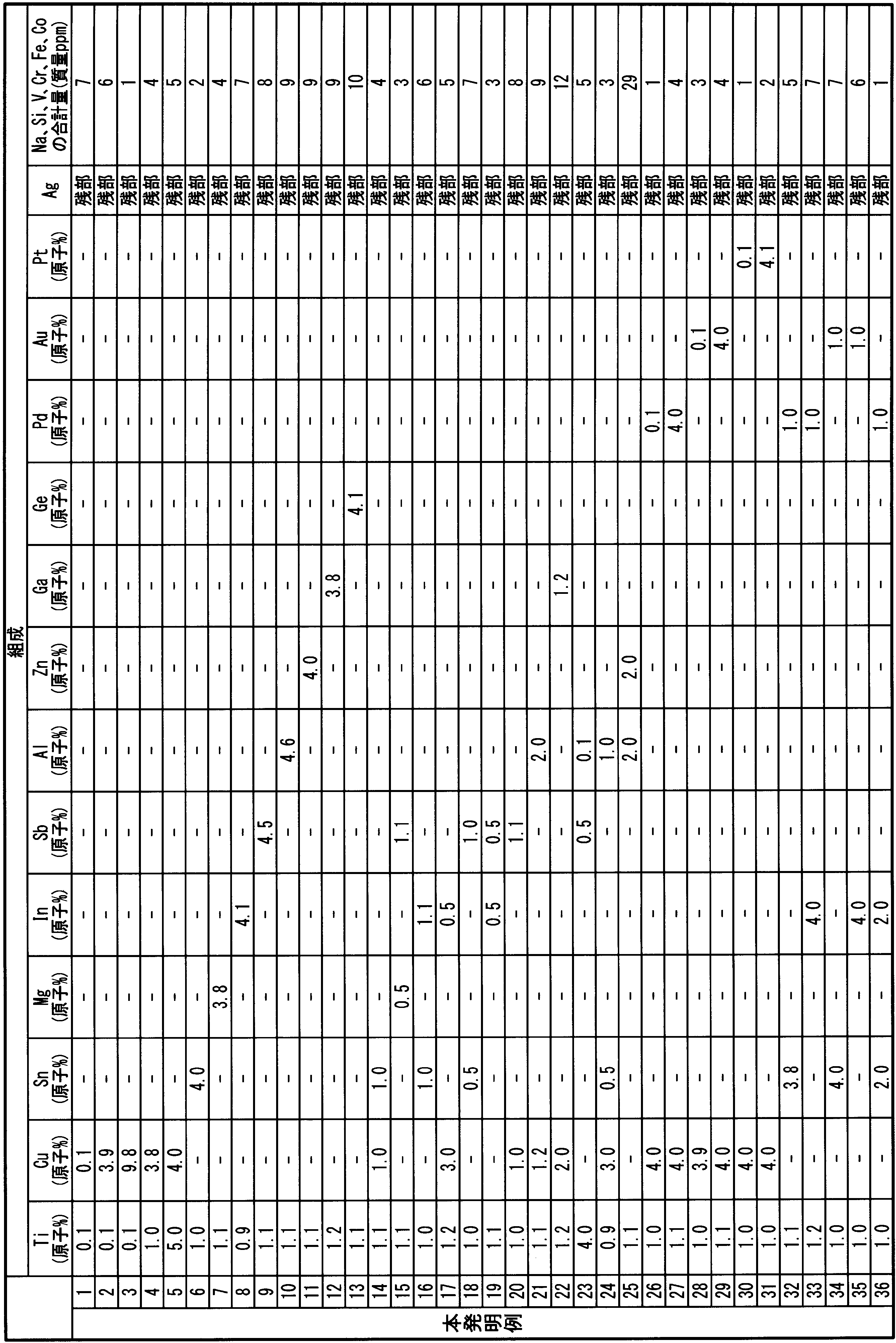
- composition analysis As for the composition of the target, a sample for analysis was collected from the Ag alloy ingot after casting, and the sample was analyzed by ICP emission spectroscopy. The analysis results are shown in Tables 1A and 1B. In each of the following examples, it was confirmed by ICP emission spectroscopy that the composition of the film was almost the same as the composition of the target used.
- Triangular specimen pieces having a side of about 10 mm were collected from 16 points evenly within the sputtering surface of the target.
- the sputter surface of each sample piece was polished.
- polishing was performed with water resistant paper of # 180 to # 4000, and then buffed with abrasive grains of 3 ⁇ m to 1 ⁇ m.
- etching was performed to such an extent that the grain boundaries could be seen with an optical microscope.
- a mixed liquid of hydrogen peroxide water and ammonia water was used as an etching solution, which was immersed for 1 to 2 seconds at room temperature to reveal grain boundaries.
- a photograph was taken with an optical microscope for each sample.
- a magnification (60 to 120 times) at which crystal grains can be easily counted was selected.
- a total of four 60 mm line segments were drawn vertically and horizontally at intervals of 20 mm in a grid pattern (as indicated by symbol #), and the number of crystal grains cut along each straight line was counted.
- the number of crystal grains at the end of the line segment was counted as 0.5.
- the average intercept length: L ( ⁇ m), L 60000 / (MN) (where M is the actual magnification, and N is the average value of the number of crystal grains cut by each straight line) I asked for it.
- the average value of the average particle diameter d ( ⁇ m) of the samples sampled from 16 locations was used as the crystal grain diameter of the target silver alloy crystal.
- the variation in particle size was calculated as follows. Of the 16 average particle diameters obtained at 16 locations, the absolute value of deviation from the average value of the average particle sizes (
- the target was consumed by repeating the sputter
- Table 2 shows the number of abnormal discharges for one hour from the start of discharge as “number of abnormal discharges after one hour” and the number of abnormal discharges generated in 30 minutes after consumption as “number of abnormal discharges after consumption”.
- Comparative Example 15 in which the total content of Na, Si, V, Cr, Fe, and Co exceeds 100 mass ppm, the number of abnormal discharges after 1 hour is 34 times / h, and the number of abnormal discharges after consumption is 41 times / 30 minutes. The number of spatters increased, and sputtering could not be performed stably. Further, in Examples 22 and 25 of the present invention in which the total content of Na, Si, V, Cr, Fe, and Co exceeds 10 mass ppm, the number of abnormal discharges after 1 hour and the number of abnormal discharges after consumption are slightly increased. Was confirmed. Furthermore, in Comparative Examples 1, 3, and 9 in which the variation in the grain size of the Ag alloy crystal exceeds 20%, it was confirmed that the number of abnormal discharges after consumption slightly increased.
- Example 2 Production of an Ag alloy film (semi-permeable membrane) [Invention Examples 101 to 139, Comparative Examples 101 to 115]
- the Ag alloy sputtering target produced in Example 1 was attached to a sputtering apparatus, and sputtering was performed under the following conditions to form an Ag alloy film having a thickness of 10 nm on the surface of the glass substrate.
- Comparative Example 101 using an Ag alloy sputtering target (Comparative Example 1) with a Ti content of less than 0.1 atomic%, the sheet resistance greatly increased before and after the sulfidation test, and the transmittance decreased significantly. Discoloration, spots, etc. occurred in the Ag alloy film after the sulfidation test. Furthermore, the Ag alloy film disappeared after the salt water test.
- Comparative Example 102 using an Ag alloy sputtering target (Comparative Example 2) having a Ti content greater than 5.0 atomic%, the sheet resistance greatly increased before and after the sulfidation test, and the transmittance decreased significantly. Discoloration, spots, etc. occurred in the Ag alloy film after the sulfidation test. Furthermore, the Ag alloy film disappeared after the salt water test.
- An Ag alloy sputtering target (Comparative Examples 3, 5, 7, 9, 11, 13) in which the total content of Cu, Sn, Mg, In, Sb, Al, Zn, Ge, and Ga is less than 0.1 atomic%.
- the sheet resistance increased greatly before and after the constant temperature and humidity test, the transmittance decreased greatly, and the Ag alloy film after the constant temperature and humidity test showed Discoloration, spots, etc. occurred.
- Ag alloy sputtering target having a total content of Cu, Sn, Mg, In, Sb, Al, Zn, Ge, and Ga of more than 10.0 atomic% in total with Ti (Comparative Examples 4, 6, 8, 10, 12) In Comparative Examples 104, 106, 108, 110, 112, and 114 using 14), the sheet resistance after film formation is greater than 30 ⁇ / ⁇ ( ⁇ / sq.) And the transmittance is greater than 60%. Was also low.
- Comparative Example 115 using an Ag alloy sputtering target (Comparative Example 15) in which the total content of Na, Si, V, Cr, Fe, and Co is more than 100 ppm by mass, the sheet resistance greatly increases before and after the sulfidation test. However, the transmittance was greatly reduced, and discoloration, spots, etc. occurred in the Ag alloy film after the sulfidation test. Furthermore, the Ag alloy film disappeared after the salt water test.
- the total content of Na, Si, V, Cr, Fe, Co is 100 mass ppm or less.
- the sheet resistance after film formation is less than 30 ⁇ / ⁇ , and the transmittance exceeds 60%. It was.
- the sheet resistance and transmittance do not change significantly before and after the test, and further, no discoloration, spots, etc. occur in the Ag alloy film after the test. It was stable.
- Invention Examples 126 to 128 in which film formation was performed in a mixed gas atmosphere of Ar and oxygen Invention Example 124 in which film formation was performed in an Ar gas atmosphere using the same Ag alloy sputtering target.
- the sheet resistance after film formation is small and the transmittance is high, and the changes in sheet resistance and transmittance are generally small in any of the constant temperature and humidity test, the sulfidation test, and the salt water test. Corrosion improved.
- a total of at least one element selected from Pd, Pt, and Au is 0.1 atomic percent or more and a total of Ti, Cu, Sn, Mg, In, Sb, Al, Zn, Ge, and Ga is 10.
- Invention Examples 129 to 139 using Ag alloy sputtering targets contained in a range of 0 atomic% or less, changes in sheet resistance and transmittance before and after the sulfidation test and the salt water test Became smaller.
- an Ag alloy film having low resistance, high transmittance, excellent heat resistance, moisture resistance, sulfur resistance, and chlorine resistance and suitable as a translucent electrode film is obtained. It was confirmed that it could be provided.
- Example 3 Production of Ag Alloy Film (Reflection Film) [Invention Examples 140 to 141, Comparative Examples 116 to 117]
- the Ag alloy sputtering target produced in Example 1 was mounted on a sputtering apparatus, and sputtering was performed under the same conditions as in Example 2 to form an Ag alloy film having a thickness of 100 nm on the surface of the glass substrate.
- the Ag alloy film was evaluated in the same procedure as described above.
- the contents are shown in Table 5.
- “post-deposition reflectance” in Table 5 is a value obtained by measuring the reflectance of the obtained Ag alloy film using a spectrophotometer.
- the numerical value shown in the table is the reflectance of light having a wavelength of 550 nm.
- Comparative Example 116 using an Ag alloy sputtering target (Comparative Example 1) in which the Ti content is less than 0.1 atomic%, the sheet resistance is greatly increased before and after the sulfidation test, and the reflectance is greatly decreased. Discoloration, spots, etc. occurred in the Ag alloy film after the sulfidation test. Furthermore, the Ag alloy film disappeared after the salt water test.
- Comparative Example 117 using an Ag alloy sputtering target (Comparative Example 2) with a Ti content greater than 5.0 atomic%, the sheet resistance greatly increased before and after the sulfidation test, and the reflectance decreased significantly. Discoloration, spots, etc. occurred in the Ag alloy film after the sulfidation test. Furthermore, the Ag alloy film disappeared after the salt water test.
- the total content of Na, Si, V, Cr, Fe, Co is 100 mass ppm or less.
- the present invention example 141 in which film formation was performed in a mixed gas atmosphere of Ar and oxygen was compared with the present invention example 140 in which film formation was performed in an Ar gas atmosphere using the same Ag alloy sputtering target.
- permeability was small, and corrosion resistance improved.
- an Ag alloy film having low resistance and high transmittance, and excellent in heat resistance, moisture resistance, sulfur resistance, and chlorine resistance and suitable as a reflective electrode film is provided. It was confirmed that it was possible.
- Example 4 Production of translucent conductive laminated film (conductive oxide film / Ag alloy film / conductive oxide film) [Invention Examples 201 to 217, Comparative Examples 201 to 208]
- the Ag alloy sputtering target prepared in Example 1 and the following conductive oxide film-forming target were mounted on a sputtering apparatus, and sputtering was performed under the same conditions as in Example 2 to form a 20 nm thick surface on the surface of the glass substrate.
- a semitransparent conductive laminated film in which a conductive oxide (A) film, a 10 nm thick Ag alloy film (semitransparent film), and a 20 nm thick conductive oxide (B) film are laminated in this order.
- a semitransparent conductive laminated film was evaluated in the same manner as the evaluation of the Ag alloy film of Example 2.
- the contents are shown in Tables 6 and 7.
- ITO 90 mol% indium oxide
- 10 mol% tin oxide IZO 70 mol% indium oxide
- AZO Aluminum oxide 2 mol%
- GZO Gallium oxide 2 mol%
- Zinc oxide 98 mol% Note that the conductive oxide film was formed in an Ar gas atmosphere containing 2% oxygen.
- Comparative Examples 201, 203, 205, and 207 using an Ag alloy sputtering target (Comparative Example 1) with a Ti content of less than 0.1 atomic% the conductive oxides (A) and (B) Even before and after the sulfidation test, the sheet resistance was greatly increased, the transmittance was greatly decreased, and the edge of the Ag alloy film after the sulfidation test was discolored. Furthermore, the Ag alloy film disappeared after the salt water test.
- Comparative Examples 202, 204, 206, and 208 using an Ag alloy sputtering target (Comparative Example 2) having a Ti content greater than 5.0 atomic%
- the conductive oxides (A) and (B) are either Even so, the sheet resistance after film formation was larger than 30 ⁇ / ⁇ , and the transmittance was lower than 80%.
- the sheet resistance greatly increased before and after the sulfidation test, the transmittance was greatly decreased, and the edge of the Ag alloy film after the sulfidation test was discolored. Furthermore, the Ag alloy film disappeared after the salt water test.
- the total content of Na, Si, V, Cr, Fe, Co is 100 mass ppm or less
- the sheet resistance after film formation is 30 ⁇ / ⁇ in all cases.
- the transmittance exceeded 80%.
- the sheet resistance and transmittance do not change significantly before and after the test, and further, no discoloration, spots, etc. occur in the laminated film after the test. It was stable.
- Invention Examples 208 to 210 in which film formation was performed in a mixed gas atmosphere of Ar and oxygen Invention Example 204 in which film formation was performed in an Ar gas atmosphere using the same Ag alloy sputtering target. Compared with, sheet resistance after film formation is low, and transmittance after film formation is generally high, and changes in sheet resistance and transmittance are generally small in any of the constant temperature and humidity test, the sulfide test, and the salt water test. , Stability improved.
- the Ag alloy film according to the present invention is stable and resistant to corrosion even when used as a semitransparent conductive laminated film with a conductive oxide film.
- Example 5 Production of reflective conductive laminated film (conductive oxide film / Ag alloy film / conductive oxide film) [Invention Examples 218 to 219, Comparative Examples 209 to 210]
- the Ag alloy sputtering target produced in Example 1 and the following conductive oxide film-forming target were mounted on a sputtering apparatus, and sputtering was performed under the same conditions as in Example 4 so that the surface of the glass substrate had a thickness of 20 nm.
- a reflective conductive laminated film is formed by laminating a conductive oxide (A) film, a 100 nm thick Ag alloy film (reflective film), and a 20 nm thick conductive oxide (B) film in this order.
- the reflective conductive laminated film was evaluated in the same manner as the evaluation of the Ag alloy film of Example 3. The contents are shown in Table 8.
- Comparative Example 209 using an Ag alloy sputtering target (Comparative Example 1) having a Ti content of less than 0.1 atomic%, the sheet resistance increases before and after the sulfidation test, the reflectivity decreases, and after the sulfidation test. The edge of the Ag alloy film was discolored. Furthermore, the Ag alloy film disappeared after the salt water test.
- Comparative Example 210 using an Ag alloy sputtering target (Comparative Example 2) having a Ti content greater than 5.0 atomic%, the sheet resistance after film formation was high and the reflectance was low. Further, the sheet resistance increased before and after the sulfidation test, the reflectance decreased, and the edge of the Ag alloy film after the sulfidation test was discolored. Furthermore, the Ag alloy film disappeared after the salt water test.
- the total content of Na, Si, V, Cr, Fe, Co is 100 mass ppm or less
- Invention Examples 218 and 219 using a certain Ag alloy sputtering target Invention Example 14, the sheet resistance after film formation was small, and the reflectance exceeded 94%.
- the sheet resistance and transmittance do not change greatly before and after the test, and further, no discoloration, spots, etc. occur in the Ag alloy film after the test. It was stable.
- the Ag alloy film according to the present invention is stable and resistant to corrosion even when used as a reflective conductive laminated film laminated with a conductive oxide film.
- the Ag alloy film of the present invention has excellent optical characteristics and electrical conductivity immediately after the film formation, and the optical characteristics and electrical conductivity do not change greatly even in a hot and humid environment. Corrosion does not easily occur, and even when an ultra-thin film is formed, aggregation does not easily occur.
Landscapes
- Chemical & Material Sciences (AREA)
- Engineering & Computer Science (AREA)
- Materials Engineering (AREA)
- Mechanical Engineering (AREA)
- Metallurgy (AREA)
- Organic Chemistry (AREA)
- Chemical Kinetics & Catalysis (AREA)
- Physical Vapour Deposition (AREA)
Abstract
本発明のAg合金膜は、Tiを0.1原子%以上5.0原子%以下、Cu、Sn、Mg、In、Sb、Al、Zn、Ge、Gaから選ばれる少なくとも1種の元素を合計で0.1原子%以上かつTiとの総計で10.0原子%以下となる範囲で含有し、残部がAgと不可避不純物からなり、Na、Si、V、Cr、Fe、Coの合計含有量が100質量ppm以下である。
Description
本発明は、Ag合金膜とその製造方法、及びそのAg合金膜の製造に用いることができるAg合金スパッタリングターゲットに関する。また、本発明は、Ag合金膜を含む積層膜に関する。
本願は、2015年7月28日に日本に出願された特願2015-148474号、及び2016年7月1日に日本に出願された特願2016-131593号に基づき優先権を主張し、その内容をここに援用する。
本願は、2015年7月28日に日本に出願された特願2015-148474号、及び2016年7月1日に日本に出願された特願2016-131593号に基づき優先権を主張し、その内容をここに援用する。
Ag膜は、高い光の反射率と低い抵抗値を示すことから、有機EL素子、反射型液晶ディスプレイ、LED、太陽電池などの反射電極膜として利用されている。また、Ag膜は薄膜化することによって高い透過率を示すことから、薄膜化したAg膜はタッチパネルの半透明電極膜として利用されている。Ag膜から形成された反射電極膜及び半透明電極膜は、ITO膜やIZO膜などの導電性酸化物との積層膜として利用されることもある。
Ag膜は、上記のとおり、光の反射率や薄膜化したときの光の透過率が高いという優れた光学特性と、抵抗値が低いという優れた導電性とを有する。しかし、Ag膜は、熱湿環境(高温高湿の環境)においては光学特性と導電性が低下しやすいこと、塩素や硫黄との反応性が高い、即ち塩素や硫黄に対する耐腐食性が低いこと、さらには凝集しやすいことが知られている。そこで、Ag膜の光学特性及び導電性を長期間にわたって安定させること、耐腐食性を向上させること、そして凝集の発生を防止することなどを目的として、Ag膜にAg以外の金属元素を添加して、Ag合金膜とすることが行われている。
特許文献1には、長期間での反射率の維持などを目的として、種々の金属元素を添加した反射膜用のAg合金が記載されている。特許文献2には、耐食性、反射率、抵抗及び耐熱性などの向上を目的として、種々の金属元素を添加したAg合金が記載されている。特許文献3には、反射率の向上、湿度や熱によるAgの凝集の発生防止などを目的として、種々の金属元素を添加したAg合金反射膜が記載されている。特許文献4には、スパッタリングに用いる場合にプリスパッタの回数を低減してプリスパッタ時間を短縮することを目的として、種々の金属元素を添加したAg基合金スパッタリングターゲットが記載されている。
ところで、上述のとおり、Ag膜にAg以外の金属元素を添加して、Ag合金膜とすることが行われているが、金属元素を添加することによって、Agが有する優れた光学特性と導電性が損なわれることがある。また、半透明電極膜として用いるAg合金膜では、透過率の向上のためにさらなる薄膜化が要求されているが、Ag膜は厚さが薄くなると、特に厚さが20nm以下の超薄膜となると、凝集して島状になりやすくなるという問題がある。
さらに、Ag合金膜を、ITO膜やIZO膜などの導電性酸化物と積層すると、Ag合金膜と導電性酸化膜との間に電位差が生じることによってAg合金膜の腐食が促進されることがあるという問題がある。
この発明は、前述した事情に鑑みてなされたものであって、成膜直後は優れた光学特性と導電性とを有し、かつ、熱湿環境下においてもその光学特性と導電性とが大きく変化することがなく、塩素や硫黄による腐食がおこりにくく、さらに超薄膜にしても凝集が起こりにくいAg合金膜とその製造方法、さらにそのAg合金膜の製造に用いることができるAg合金スパッタリングターゲットを提供することにある。さらに、この発明は、Ag合金膜の腐食が起こりにくい、Ag合金膜と透明導電性酸化物との積層膜を提供することもその目的とする。
上記課題を解決するために、本発明のAg合金膜は、Tiを0.1原子%以上5.0原子%以下の範囲で含有し、Cu、Sn、Mg、In、Sb、Al、Zn、Ge、Gaから選ばれる少なくとも1種の元素を合計で0.1原子%以上かつTiとの総計で10.0原子%以下となる範囲で含有し、残部がAgと不可避不純物からなり、Na、Si、V、Cr、Fe、Coの合計含有量が100質量ppm以下であることを特徴としている。
この構成のAg合金膜はTiを0.1原子%以上含有するので、Ag合金膜の耐硫黄性及び耐塩素性が向上する。その理由は明らかでないが、このAg合金膜をスパッタリング法等により成膜すると、Tiが膜内部で酸化することで、Tiの酸化物が自己形成され、効果の発現に寄与しているものと考えられる。
また、このAg合金膜は、Tiの含有量が5.0原子%以下に制限されているので、Agが有する優れた光学特性と導電性を確保できる。さらに、このAg合金膜は、Na、Si、V、Cr、Fe、Coの合計含有量が100質量ppm以下に制限されている。この制限によって、これらの金属元素が、Ag結晶の粒界表面に酸化物として存在する量が少なくなり、Tiの酸化物が存在するAg結晶の粒界表面が広くなるので、Ag合金膜の耐硫黄性及び耐塩素性が向上する。
また、このAg合金膜は、Tiの含有量が5.0原子%以下に制限されているので、Agが有する優れた光学特性と導電性を確保できる。さらに、このAg合金膜は、Na、Si、V、Cr、Fe、Coの合計含有量が100質量ppm以下に制限されている。この制限によって、これらの金属元素が、Ag結晶の粒界表面に酸化物として存在する量が少なくなり、Tiの酸化物が存在するAg結晶の粒界表面が広くなるので、Ag合金膜の耐硫黄性及び耐塩素性が向上する。
また、Cu、Sn、Mg、In、Sb、Al、Zn、Ge、Gaといった金属元素はAg合金膜中でAg原子の移動(凝集)を抑制するため、これらの金属元素を0.1原子%以上含有することによって、Ag合金膜の熱湿環境下での光学特性及び導電性の安定性が向上し、またさらにAg合金膜を薄膜にしても凝集が起こりにくくなる。また、これらの金属元素の含有量がTiとの総計で10.0原子%以下となる範囲と制限されているので、成膜直後のAg合金膜の優れた光学特性と導電性とを確保できるとともに、熱湿環境下での光学特性及び導電性が大きく変化することを抑制できる。
ここで、本発明のAg合金膜においては、Tiの含有量Aと、Cu、Sn、Mg、In、Sb、Al、Zn、Ge、Gaの合計含有量Bとの原子比A/Bが、0.1以上6.0以下の範囲にあることが好ましい。
この場合、理由は明らかではないが、Tiの含有量Aと、Cu、Sn、Mg、In、Sb、Al、Zn、Ge、Gaの合計含有量Bとの原子比A/Bが、0.1以上6.0以下の範囲とされているので、Tiがより効果的に作用して、Ag合金膜の耐硫黄性及び耐塩素性が向上する。
この場合、理由は明らかではないが、Tiの含有量Aと、Cu、Sn、Mg、In、Sb、Al、Zn、Ge、Gaの合計含有量Bとの原子比A/Bが、0.1以上6.0以下の範囲とされているので、Tiがより効果的に作用して、Ag合金膜の耐硫黄性及び耐塩素性が向上する。
また、本発明のAg合金膜においては、さらに、Pd、Pt、Auから選ばれる少なくとも1種の元素を合計で0.1原子%以上かつTi、Cu、Sn、Mg、In、Sb、Al、Zn、Ge、Gaとの総計で10.0原子%以下となる範囲で含有していてもよい。
この場合、Pd、Pt、Auといった化学安定性の高い貴金属元素が、合計で0.1原子%以上かつTi、Cu、Sn、Mg、In、Sb、Al、Zn、Ge、Gaとの総計で10.0原子%以下となる範囲で含有されるので、Ag合金そのものの化学安定性が向上し、Ag合金膜の耐塩素性及び耐硫黄性が向上する。
この場合、Pd、Pt、Auといった化学安定性の高い貴金属元素が、合計で0.1原子%以上かつTi、Cu、Sn、Mg、In、Sb、Al、Zn、Ge、Gaとの総計で10.0原子%以下となる範囲で含有されるので、Ag合金そのものの化学安定性が向上し、Ag合金膜の耐塩素性及び耐硫黄性が向上する。
さらに、本発明のAg合金膜においては、膜厚が20nm以下であってもよい。
この場合、Ag合金膜は、膜厚が20nm以下の超薄膜であっても凝集して島状になりにくいので、光の透過率が高くなる。
この場合、Ag合金膜は、膜厚が20nm以下の超薄膜であっても凝集して島状になりにくいので、光の透過率が高くなる。
本発明の積層膜は、上記のAg合金膜と、該Ag合金膜の片面または両面に形成された導電性酸化物膜とを備えることを特徴としている。
この構成の積層膜では、Ag合金膜内のAg結晶の表面あるいは粒界がTi酸化物によって保護されているので、Ag合金膜と透明導電性酸化物膜との間に生じる電食作用が抑制されて、Ag合金膜の腐食が起こりにくくなる。
この構成の積層膜では、Ag合金膜内のAg結晶の表面あるいは粒界がTi酸化物によって保護されているので、Ag合金膜と透明導電性酸化物膜との間に生じる電食作用が抑制されて、Ag合金膜の腐食が起こりにくくなる。
本発明のAg合金スパッタリングターゲットは、Tiを0.1原子%以上5.0原子%以下、Cu、Sn、Mg、In、Sb、Al、Zn、Ge、Gaから選ばれる少なくとも1種の元素を合計で0.1原子%以上かつTiとの総計が10.0原子%以下となる範囲で含有し、残部がAgと不可避不純物からなり、Na、Si、V、Cr、Fe、Coの合計含有量が100質量ppm以下であることを特徴としている。
この構成のAg合金スパッタリングターゲットを用いて、スパッタリング法によって成膜されたAg合金膜は、光の反射率あるいは透過率が高く優れた光学特性を有するとともに、抵抗値が低く優れた導電性を有し、かつ、熱湿環境下においてもその光学特性及び導電性が大きく変化することがなく、塩素や硫黄による腐食がおこりにくく、さらに超薄膜にしても凝集が起こりにくくなる。さらに、この構成のAg合金スパッタリングターゲットは、Na、Si、V、Cr、Fe、Coの合計含有量が100質量ppm以下に制限されているので、スパッタリング法による成膜時に異常放電が起こりにくくなる。
ここで、本発明のAg合金スパッタリングターゲットにおいては、Tiの含有量Aと、Cu、Sn、Mg、In、Sb、Al、Zn、Ge、Gaの合計含有量Bとの原子比A/Bが、0.1以上6.0以下の範囲にあることが好ましい。
この場合、このAg合金スパッタリングターゲットを用いて成膜されるAg合金膜の耐硫黄性及び耐塩素性が向上する。
この場合、このAg合金スパッタリングターゲットを用いて成膜されるAg合金膜の耐硫黄性及び耐塩素性が向上する。
また、本発明のAg合金スパッタリングターゲットにおいては、さらに、Pd、Pt、Auから選ばれる少なくとも1種の元素を合計で0.1原子%以上かつTi、Cu、Sn、Mg、In、Sb、Al、Zn、Ge、Gaとの総計で10.0原子%以下となる範囲で含有していてもよい。
この場合、このAg合金スパッタリングターゲットを用いて成膜されるAg合金膜の耐塩水性及び耐硫化性が向上する。
この場合、このAg合金スパッタリングターゲットを用いて成膜されるAg合金膜の耐塩水性及び耐硫化性が向上する。
さらに、本発明のAg合金スパッタリングターゲットにおいては、前記Na、Si、V、Cr、Fe、Coの合計含有量が10質量ppm以下であることが好ましい。
この場合、スパッタリング法による成膜時に異常放電がさらに起こりにくくなる。
この場合、スパッタリング法による成膜時に異常放電がさらに起こりにくくなる。
さらにまた、本発明のAg合金スパッタリングターゲットにおいては、複数のAg合金結晶を含む多結晶体であって、前記Ag合金結晶の粒径を複数の箇所において測定した結果、測定した全てのAg合金結晶の粒径の平均値である平均結晶粒径Cと、測定した各箇所でのAg合金結晶の粒径の平均値Dのうち、前記平均結晶粒径Cの偏差の絶対値が最大となる平均値Dmaxとから定義されるAg合金結晶粒径のばらつきE(%)=(Dmax-C)/C×100が20%以内であることが好ましい。
この場合、Ag合金スパッタリングターゲットのAg合金結晶粒径のばらつきが小さいので、スパッタリング法による成膜時に異常放電がさらに起こりにくくなる。
この場合、Ag合金スパッタリングターゲットのAg合金結晶粒径のばらつきが小さいので、スパッタリング法による成膜時に異常放電がさらに起こりにくくなる。
またさらに、本発明のAg合金スパッタリングターゲットにおいて、前記平均結晶粒径Cは200μm以下であることが好ましい。
この場合、スパッタリング法による成膜によってターゲットが消耗しても、スパッタ面に形成される凹凸が小さくなるので、長期間にわたって安定してスパッタリングを行うことができる。
この場合、スパッタリング法による成膜によってターゲットが消耗しても、スパッタ面に形成される凹凸が小さくなるので、長期間にわたって安定してスパッタリングを行うことができる。
本発明のAg合金膜の製造方法は、上述のAg合金スパッタリングターゲットを用いてスパッタリングを行うことを特徴としている。
本発明のAg合金膜の製造方法を用いることによって、成膜直後は優れた光学特性と導電性とを有し、かつ、熱湿環境下においてもその光学特性及び導電性が大きく変化することがなく、塩素や硫黄による腐食がおこりにくく、さらに超薄膜にしても凝集が起こりにくいAg合金膜を製造することができる。
本発明のAg合金膜の製造方法を用いることによって、成膜直後は優れた光学特性と導電性とを有し、かつ、熱湿環境下においてもその光学特性及び導電性が大きく変化することがなく、塩素や硫黄による腐食がおこりにくく、さらに超薄膜にしても凝集が起こりにくいAg合金膜を製造することができる。
ここで、本発明のAg合金膜の製造方法においては、不活性ガスの全圧に対して0.5~5%の圧力となる量の酸素を含むガス雰囲気にてスパッタリングを行うことが好ましい。
この場合、成膜時にTiの酸化物をより確実に形成させることができる。このため、熱湿環境下での光学特性及び導電性の変化が小さく、耐塩素性及び耐硫黄性がさらに向上したAg合金膜を製造できる。
この場合、成膜時にTiの酸化物をより確実に形成させることができる。このため、熱湿環境下での光学特性及び導電性の変化が小さく、耐塩素性及び耐硫黄性がさらに向上したAg合金膜を製造できる。
以上のように、本発明によれば、成膜直後の光の反射率あるいは透過率が高く優れた光学特性を有するとともに、抵抗値が低く優れた導電性を有し、かつ、熱湿環境下においてもその光学特性及び導電性が大きく変化することがなく、塩素や硫黄による腐食がおこりにくく、さらに超薄膜にしても凝集が起こりにくいAg合金膜とその製造方法、さらにそのAg合金膜の製造に用いることができるAg合金スパッタリングターゲットを提供することが可能になる。さらに、本発明によれば、Ag合金膜の腐食が起こりにくい、Ag合金膜と導電性酸化物との積層膜を提供することが可能となる。
<Ag合金膜>
以下に、本発明の一実施形態であるAg合金膜について説明する。
本実施形態であるAg合金膜は、例えば、有機EL素子、反射型液晶ディスプレイ、LED、太陽電池などの反射電極膜、タッチパネルの半透明電極膜として使用できる。また、本実施形態であるAg合金膜は、導電性酸化物膜との積層膜として利用することができる。
以下に、本発明の一実施形態であるAg合金膜について説明する。
本実施形態であるAg合金膜は、例えば、有機EL素子、反射型液晶ディスプレイ、LED、太陽電池などの反射電極膜、タッチパネルの半透明電極膜として使用できる。また、本実施形態であるAg合金膜は、導電性酸化物膜との積層膜として利用することができる。
本実施形態のAg合金膜は、膜厚が20nm以下の超薄膜であっても凝集して島状になりにくい。このため、本実施形態のAg合金膜は、膜厚が20nm以下の半透明電極膜として特に有利に用いることができる。Ag合金膜の膜厚は、5nm以上であることが好ましい。Ag合金膜の厚さが5nm未満の場合には、導電性を確保できなくなるおそれがある。
本実施形態であるAg合金膜は、Tiを0.1原子%以上5.0原子%以下、Cu、Sn、Mg、In、Sb、Al、Zn、Ge、Gaから選ばれる少なくとも1種の元素を合計で0.1原子%以上かつTiとの総計で10.0原子%以下となる範囲で含有し、残部がAgと不可避不純物からなり、Na、Si、V、Cr、Fe、Coの合計含有量が100質量ppm以下である。さらに、Pd、Pt、Auから選ばれる少なくとも1種の元素を合計で0.1原子%以上かつTi、Cu、Sn、Mg、In、Sb、Al、Zn、Ge、Gaとの総計で10.0原子%以下となる範囲で含有していてもよい。
以下に、Ag合金膜の組成、膜厚を上述のように規定した理由について説明する。
以下に、Ag合金膜の組成、膜厚を上述のように規定した理由について説明する。
(Ti)
Tiは、Ag合金膜の表面もしくは内部にTiの酸化物として存在していることが好ましい。このTiの酸化物は、Ag合金膜を硫黄や塩素から保護する作用がある。すなわち、Tiは、Ag合金膜の耐硫黄性と耐塩素性とを向上させる作用効果を有する元素である。
Ti酸化物は、Ag合金膜の表面に層状に存在していてもよい。なお、Ag合金膜が薄い場合、通常の測定ではTiの酸化物層の存在を確認することが困難になる場合があるが、この場合でも本実施形態のAg合金膜は十分な耐硫黄性及び耐塩素性を示す。測定困難な薄さのTiの酸化物層であっても、効果の発現に寄与するものと考えられる。
ここで、Ag合金膜のTi含有量が0.1原子%未満の場合には、耐硫黄性及び耐塩素性が十分に向上しない。一方、Tiの含有量が5.0原子%を超えた場合には、成膜直後のAg合金膜の光の透過率または反射率が低下し、また抵抗値が高くなることがある。さらに、Tiの含有量が5.0原子%を超えた場合には、Ti酸化物の自己形成が阻害されて、耐硫黄性及び耐塩素性が十分に向上しないことがある。
このような理由から、本実施形態のAg合金膜では、Tiの含有量を、0.1原子%以上5.0原子%以下の範囲に設定している。なお、上述の作用効果を確実に発揮させるために、Ag合金膜におけるTiの含有量は、0.2原子%以上3.0原子%以下の範囲とすることが好ましく、0.5原子%以上2.0原子%以下の範囲とすることがより好ましい。
Tiは、Ag合金膜の表面もしくは内部にTiの酸化物として存在していることが好ましい。このTiの酸化物は、Ag合金膜を硫黄や塩素から保護する作用がある。すなわち、Tiは、Ag合金膜の耐硫黄性と耐塩素性とを向上させる作用効果を有する元素である。
Ti酸化物は、Ag合金膜の表面に層状に存在していてもよい。なお、Ag合金膜が薄い場合、通常の測定ではTiの酸化物層の存在を確認することが困難になる場合があるが、この場合でも本実施形態のAg合金膜は十分な耐硫黄性及び耐塩素性を示す。測定困難な薄さのTiの酸化物層であっても、効果の発現に寄与するものと考えられる。
ここで、Ag合金膜のTi含有量が0.1原子%未満の場合には、耐硫黄性及び耐塩素性が十分に向上しない。一方、Tiの含有量が5.0原子%を超えた場合には、成膜直後のAg合金膜の光の透過率または反射率が低下し、また抵抗値が高くなることがある。さらに、Tiの含有量が5.0原子%を超えた場合には、Ti酸化物の自己形成が阻害されて、耐硫黄性及び耐塩素性が十分に向上しないことがある。
このような理由から、本実施形態のAg合金膜では、Tiの含有量を、0.1原子%以上5.0原子%以下の範囲に設定している。なお、上述の作用効果を確実に発揮させるために、Ag合金膜におけるTiの含有量は、0.2原子%以上3.0原子%以下の範囲とすることが好ましく、0.5原子%以上2.0原子%以下の範囲とすることがより好ましい。
(Cu、Sn、Mg、In、Sb、Al、Zn、Ge、Ga)
Cu、Sn、Mg、In、Sb、Al、Zn、Ge、Gaは、主としてAg合金膜内に存在して、成膜されたAg合金膜の熱湿環境下での光学特性及び導電性の安定性を向上させる効果とAg合金膜の凝集の発生を抑える作用効果とがある。
ここで、Cu、Sn、Mg、In、Sb、Al、Zn、Ge、Gaから選ばれる少なくとも1種の元素の合計含有量が0.1原子%未満の場合には、熱湿環境下での光学特性及び導電性の安定性が充分に向上せず、またAg合金膜の凝集の発生が起こりやすくなる。
一方、これらの金属元素の含有量がTiとの総計で10.0原子%を超えると、成膜直後のAg合金膜の光の透過率もしくは反射率が低下し、また抵抗値が高くなることがある。
このような理由から、本実施形態のAg合金膜では、Cu、Sn、Mg、In、Sb、Al、Zn、Ge、Gaから選ばれる少なくとも1種の元素の合計含有量を0.1原子%以上かつTiとの総計で10.0原子%以下となる範囲に設定している。なお、上述の作用効果を確実に発揮させるために、Ag合金膜における上記金属元素の合計含有量は、0.2原子%以上かつTiとの総計で7.0原子%以下の範囲とすることが好ましく、0.5原子%以上かつTiとの総計で5.0原子%以下の範囲とすることがより好ましい。
Cu、Sn、Mg、In、Sb、Al、Zn、Ge、Gaは、主としてAg合金膜内に存在して、成膜されたAg合金膜の熱湿環境下での光学特性及び導電性の安定性を向上させる効果とAg合金膜の凝集の発生を抑える作用効果とがある。
ここで、Cu、Sn、Mg、In、Sb、Al、Zn、Ge、Gaから選ばれる少なくとも1種の元素の合計含有量が0.1原子%未満の場合には、熱湿環境下での光学特性及び導電性の安定性が充分に向上せず、またAg合金膜の凝集の発生が起こりやすくなる。
一方、これらの金属元素の含有量がTiとの総計で10.0原子%を超えると、成膜直後のAg合金膜の光の透過率もしくは反射率が低下し、また抵抗値が高くなることがある。
このような理由から、本実施形態のAg合金膜では、Cu、Sn、Mg、In、Sb、Al、Zn、Ge、Gaから選ばれる少なくとも1種の元素の合計含有量を0.1原子%以上かつTiとの総計で10.0原子%以下となる範囲に設定している。なお、上述の作用効果を確実に発揮させるために、Ag合金膜における上記金属元素の合計含有量は、0.2原子%以上かつTiとの総計で7.0原子%以下の範囲とすることが好ましく、0.5原子%以上かつTiとの総計で5.0原子%以下の範囲とすることがより好ましい。
(Na、Si、V、Cr、Fe、Co)
Na、Si、V、Cr、Fe、Coは、不可避不純物として含まれている金属元素である。これらの金属元素は、Agに対する固溶度が小さいため、Ag合金膜の結晶粒界に偏析しやすく、更にはその元素が溶解雰囲気中の残留酸素と結び付いて酸化物となり、これらの酸化物がAg合金膜組織中に介在することでTiの酸化膜自己形成を阻害する。このため、これらの金属元素の合計含有量が100質量ppmを超えるとTiによる耐食性が十分に発揮されず耐塩素性及び耐硫黄性が不十分となる。
このような理由から、本実施形態のAg合金膜では、不可避不純物のうちNa、Si、V、Cr、Fe、Coの合計含有量を100質量ppm以下に制限している。上述の作用効果を確実に発揮させるために、Ag合金膜における上記金属元素の合計含有量を30質量ppm以下の範囲とすることが好ましく、10質量ppm以下の範囲とすることがより好ましいが、これに限定されない。また、過度な低減は製造コストの増加を招来するため、Ag合金膜における上記金属元素の合計含有量の下限値を1質量ppmとすることが好ましく、5質量ppmとすることがより好ましいが、これに限定されない。
なお、Na、Si、V、Cr、Fe、Co以外の不可避不純物はTiによる耐食性を向上させる効果を阻害しない又はほとんど阻害しないので、これらを過度に低減する必要はなく、その合計含有量を1質量ppm以上1000質量ppm以下の範囲とすればよいが、これに限定されない。
Na、Si、V、Cr、Fe、Coは、不可避不純物として含まれている金属元素である。これらの金属元素は、Agに対する固溶度が小さいため、Ag合金膜の結晶粒界に偏析しやすく、更にはその元素が溶解雰囲気中の残留酸素と結び付いて酸化物となり、これらの酸化物がAg合金膜組織中に介在することでTiの酸化膜自己形成を阻害する。このため、これらの金属元素の合計含有量が100質量ppmを超えるとTiによる耐食性が十分に発揮されず耐塩素性及び耐硫黄性が不十分となる。
このような理由から、本実施形態のAg合金膜では、不可避不純物のうちNa、Si、V、Cr、Fe、Coの合計含有量を100質量ppm以下に制限している。上述の作用効果を確実に発揮させるために、Ag合金膜における上記金属元素の合計含有量を30質量ppm以下の範囲とすることが好ましく、10質量ppm以下の範囲とすることがより好ましいが、これに限定されない。また、過度な低減は製造コストの増加を招来するため、Ag合金膜における上記金属元素の合計含有量の下限値を1質量ppmとすることが好ましく、5質量ppmとすることがより好ましいが、これに限定されない。
なお、Na、Si、V、Cr、Fe、Co以外の不可避不純物はTiによる耐食性を向上させる効果を阻害しない又はほとんど阻害しないので、これらを過度に低減する必要はなく、その合計含有量を1質量ppm以上1000質量ppm以下の範囲とすればよいが、これに限定されない。
(Pd、Pt、Au)
Pd、Pt、Auは、主としてAg合金膜内に存在して、成膜されたAg合金膜の耐塩素性、耐硫黄性をより向上させる効果がある。
ここで、Pd、Pt、Auから選ばれる少なくとも1種の元素の合計含有量が0.1原子%未満の場合には、耐塩素性及び耐硫黄性が充分に向上しないおそれがある。一方、これらの金属元素の合計含有量がTi、Cu、Sn、Mg、In、Sb、Al、Zn、Ge、Gaとの総計で10.0原子%を超えると、成膜直後のAg合金膜の光の透過率もしくは反射率が低下し、また抵抗値が高くなるおそれがある。
このような理由から、本実施形態のAg合金膜では、Pd、Pt、Auから選ばれる少なくとも1種の元素の合計含有量を、0.1原子%以上かつTi、Cu、Sn、Mg、In、Sb、Al、Zn、Ge、Gaとの総計で10.0原子%以下となる範囲に設定している。なお、上述の作用効果を確実に発揮させるために、Ag合金膜における上記金属元素の合計含有量は、0.2原子%以上であることが好ましく、0.5原子%以上であることがより好ましい。また、Ag合金膜における上記金属元素の合計含有量は、Ti、Cu、Sn、Mg、In、Sb、Al、Zn、Ge、Gaとの総計で7.0原子%以下であることが好ましく、5.0原子%以下であることがより好ましい。
Pd、Pt、Auは、主としてAg合金膜内に存在して、成膜されたAg合金膜の耐塩素性、耐硫黄性をより向上させる効果がある。
ここで、Pd、Pt、Auから選ばれる少なくとも1種の元素の合計含有量が0.1原子%未満の場合には、耐塩素性及び耐硫黄性が充分に向上しないおそれがある。一方、これらの金属元素の合計含有量がTi、Cu、Sn、Mg、In、Sb、Al、Zn、Ge、Gaとの総計で10.0原子%を超えると、成膜直後のAg合金膜の光の透過率もしくは反射率が低下し、また抵抗値が高くなるおそれがある。
このような理由から、本実施形態のAg合金膜では、Pd、Pt、Auから選ばれる少なくとも1種の元素の合計含有量を、0.1原子%以上かつTi、Cu、Sn、Mg、In、Sb、Al、Zn、Ge、Gaとの総計で10.0原子%以下となる範囲に設定している。なお、上述の作用効果を確実に発揮させるために、Ag合金膜における上記金属元素の合計含有量は、0.2原子%以上であることが好ましく、0.5原子%以上であることがより好ましい。また、Ag合金膜における上記金属元素の合計含有量は、Ti、Cu、Sn、Mg、In、Sb、Al、Zn、Ge、Gaとの総計で7.0原子%以下であることが好ましく、5.0原子%以下であることがより好ましい。
(膜厚)
本実施形態のAg合金膜は、膜厚が20nm以下の超薄膜であっても凝集して島状になりにくい。このため、本実施形態のAg合金膜は、膜厚が20nm以下の半透明電極膜として有利に用いることができる。
Ag合金膜の膜厚は、5nm以上であることが好ましい。Ag合金膜の厚さが5nm未満の場合には、導電性を確保できなくなるおそれがある。
本実施形態のAg合金膜は、膜厚が20nm以下の超薄膜であっても凝集して島状になりにくい。このため、本実施形態のAg合金膜は、膜厚が20nm以下の半透明電極膜として有利に用いることができる。
Ag合金膜の膜厚は、5nm以上であることが好ましい。Ag合金膜の厚さが5nm未満の場合には、導電性を確保できなくなるおそれがある。
<積層膜>
本実施形態の積層膜は、上記の本実施形態のAg合金膜と、該Ag合金膜の片面または両面に形成された導電性酸化物膜とを備える。この構成の積層膜では、Ag合金膜と導電性酸化物膜との間にTi酸化物層が介在することによって、Ag合金と導電性酸化物との間に生じる電食作用が抑制されるので、Ag合金膜の腐食が起こりにくい。
本実施形態の積層膜は、上記の本実施形態のAg合金膜と、該Ag合金膜の片面または両面に形成された導電性酸化物膜とを備える。この構成の積層膜では、Ag合金膜と導電性酸化物膜との間にTi酸化物層が介在することによって、Ag合金と導電性酸化物との間に生じる電食作用が抑制されるので、Ag合金膜の腐食が起こりにくい。
導電性酸化物膜は、透明導電性酸化物膜であることが好ましい。透明導電性酸化物膜の例としては、ITO膜(酸化インジウム+酸化錫)、IZO膜(酸化インジウム+酸化亜鉛)、AZO膜(酸化アルミニウム+酸化亜鉛)、GZO膜(酸化ガリウム+酸化亜鉛)を挙げることができる。
<Ag合金スパッタリングターゲット>
本実施形態であるスパッタリングターゲットは、Tiを0.1原子%以上5.0原子%以下、Cu、Sn、Mg、In、Sb、Al、Zn、Ge、Gaから選ばれる少なくとも1種の元素を合計で0.1原子%以上かつTiとの総計が10.0原子%以下となる範囲で含有し、残部がAgと不可避不純物からなり、Na、Si、V、Cr、Fe、Coの合計含有量が100質量ppm以下とされている。
本実施形態であるスパッタリングターゲットは、Tiを0.1原子%以上5.0原子%以下、Cu、Sn、Mg、In、Sb、Al、Zn、Ge、Gaから選ばれる少なくとも1種の元素を合計で0.1原子%以上かつTiとの総計が10.0原子%以下となる範囲で含有し、残部がAgと不可避不純物からなり、Na、Si、V、Cr、Fe、Coの合計含有量が100質量ppm以下とされている。
本実施形態のスパッタリングターゲットは、Si、V、Cr、Fe、Coの合計含有量が100質量ppm以下に制限されているので、スパッタリング法による成膜時に異常放電が起こりにくくなる。このスパッタリング法による成膜時に異常放電をより確実に抑えるためには、Na、Si、V、Cr、Fe、Coの合計含有量が10質量ppm以下であることが好ましい。
本実施形態であるスパッタリングターゲットは、さらに、Pd、Pt、Auから選ばれる少なくとも1種の元素を合計で0.1原子%以上かつTi、Cu、Sn、Mg、In、Sb、Al、Zn、Ge、Gaとの総計で10.0原子%以下となる範囲で含有していてもよい。本実施形態のスパッタリングターゲットは、Pd、Pt、Auを上記の範囲で含むので、このAg合金スパッタリングターゲットを用いて成膜されるAg合金膜は、耐塩水性及び耐硫化性が向上する。
本実施形態であるスパッタリングターゲットは、複数のAg合金結晶を含む多結晶体であることが好ましい。この場合、前記Ag合金結晶の粒径を複数の箇所(例えば、16か所)において測定した結果、測定した全てのAg合金結晶の粒径の平均値である平均結晶粒径Cと、測定した各箇所でのAg合金結晶の粒径の平均値Dのうち、前記平均結晶粒径Cの偏差の絶対値が最大となる平均値Dmaxとから定義されるAg合金結晶粒径のばらつきE(%)=(Dmax-C)/C×100(絶対値)が20%以内であることが好ましい。このAg合金結晶粒径のばらつきを小さくすることによって、スパッタリング法による成膜時に異常放電がさらに起こりにくくなる。平均結晶粒径Cは、200nm以下であることが好ましい。
ここで、上記Ag合金結晶粒径のばらつきEを正確に得るために、大きさが500μm×500μm~1000μm×1000μmの複数の領域についてAg合金結晶の粒径を測定することが好ましく、16箇所以上について測定することが好ましいが、これに限定されない。
ここで、上記Ag合金結晶粒径のばらつきEを正確に得るために、大きさが500μm×500μm~1000μm×1000μmの複数の領域についてAg合金結晶の粒径を測定することが好ましく、16箇所以上について測定することが好ましいが、これに限定されない。
<Ag合金スパッタリングターゲットの製造方法>
次に、本実施形態に係るAg合金スパッタリングターゲットの製造方法について説明する。
まず、溶解原料として、純度99.9質量%以上のAgと、純度99.9質量%以上のTi、Cu、Sn、Mg、In、Sb、Al、Zn、Ge、Gaを準備する。
次に、本実施形態に係るAg合金スパッタリングターゲットの製造方法について説明する。
まず、溶解原料として、純度99.9質量%以上のAgと、純度99.9質量%以上のTi、Cu、Sn、Mg、In、Sb、Al、Zn、Ge、Gaを準備する。
ここで、不可避不純物のうちNa、Si、V、Cr、Fe、Coの合計含有量を低減する場合には、Ag原料に含まれるこれらの元素をICP(誘導結合プラズマ)分析等によって分析し、後述するAg合金インゴットにおいてこれらの元素の合計含有量が所定の範囲となるようなAg原料を選別して使用する。なお、Na、Si、V、Cr、Fe、Coの合計含有量を確実に低減するためには、Ag原料を硝酸又は硫酸等で浸出した後、所定のAg濃度の電解液を用いて電解精錬することが好ましい。
選別されたAg原料と、添加元素(Ti、Cu、Sn、Mg、In、Sb、Al、Zn、Ge、Ga)とを、所定の組成となるように秤量する。次に、溶解炉中において、Agを高真空または不活性ガス雰囲気中で溶解し、得られた溶湯に所定量の添加元素及び硫化銀を添加する。その後、真空または不活性ガス雰囲気中で溶解して、Tiを0.1原子%以上5.0原子%以下、Cu、Sn、Mg、In、Sb、Al、Zn、Ge、Gaから選ばれる少なくとも1種の元素を合計で0.1原子%以上かつTiとの総計が10.0原子%以下となる範囲で含有し、残部がAgと不可避不純物からなり、Na、Si、V、Cr、Fe、Coの合計含有量が100質量ppm以下であるAg合金インゴットを作製する。
得られたAg合金インゴットを冷間圧延し、その圧延後のインゴットを熱処理することが好ましい。熱処理は、大気中で500~700℃の温度で行うことが好ましい。熱処理実施後、冷却速度200℃/min以上で圧延インゴットを例えば200℃程度まで急冷することが好ましい。急冷の方法としては、1分程度の水シャワーなどがある。この急冷により結晶粒の成長を抑制し結晶粒径を微細化することができる。こうして得られたAg合金の圧延板を機械加工することにより、本実施形態に係るAg合金スパッタリングターゲットを製造することができる。なお、Ag合金スパッタリングターゲットの形状に特に限定はなく、円板型、角板型でもよいし、円筒型でもよい。
<Ag合金膜の製造方法>
本実施形態のAg合金膜の製造方法では、Ag合金スパッタリングターゲットを用いてスパッタリングを行う。スパッタ装置としては、マグネトロンスパッタ方式の装置が好ましい。スパッタ装置の電源としては、直流(DC)電源、高周波(RF)電源、中周波(MF)電源、または交流(AC)電源を使用できる。
本実施形態のAg合金膜の製造方法では、Ag合金スパッタリングターゲットを用いてスパッタリングを行う。スパッタ装置としては、マグネトロンスパッタ方式の装置が好ましい。スパッタ装置の電源としては、直流(DC)電源、高周波(RF)電源、中周波(MF)電源、または交流(AC)電源を使用できる。
本実施形態のAg合金膜の製造方法では、スパッタ装置のガス雰囲気はArガス雰囲気であることが好ましい。スパッタ装置のガス雰囲気は酸素を含んでいてもよい。酸素の量は、Arガスの全圧に対して0.5~5%の圧力となる量であることが好ましい。酸素を含むガス雰囲気にてスパッタリングを行うことによって、成膜時にTiの酸化物をより確実に形成させることができる。このため、熱湿環境下での光学特性及び導電性の変化が小さく、耐塩素性及び耐硫黄性がさらに向上したAg合金膜を製造できる。
実施例1:Ag合金スパッタリングターゲットの作製
[本発明例1~36、比較例1~14]
溶解原料として、純度99.9質量%以上のAgと、純度99.9質量%以上のTi、Cu、Sn、Mg、In、Sb、Al、Zn、Ge、Ga、Pd、Pt、Auを準備した。
ここで、不純物元素の含有量を低減させるために、Ag原料を硝酸又は硫酸で浸出した後、所定のAg濃度の電解液を用いて電解精製する方法を採用した。この精製方法で不純物が低減されたAg原料について、ICP法による不純物分析を実施し、更にNa、Si、V、Cr、Fe、Coの濃度の合計量が100ppm以下であるAg原料を、スパッタリングターゲットの製造原料として選別した。
[本発明例1~36、比較例1~14]
溶解原料として、純度99.9質量%以上のAgと、純度99.9質量%以上のTi、Cu、Sn、Mg、In、Sb、Al、Zn、Ge、Ga、Pd、Pt、Auを準備した。
ここで、不純物元素の含有量を低減させるために、Ag原料を硝酸又は硫酸で浸出した後、所定のAg濃度の電解液を用いて電解精製する方法を採用した。この精製方法で不純物が低減されたAg原料について、ICP法による不純物分析を実施し、更にNa、Si、V、Cr、Fe、Coの濃度の合計量が100ppm以下であるAg原料を、スパッタリングターゲットの製造原料として選別した。
選別したAg原料と、添加するTi及びCu、Sn、Mg、In、Sb、Al、Zn、Ge、Ga、Pd、Pt、Auとを、所定の組成となるように秤量した。次に、溶解炉を用いて、Agを高真空または不活性ガス雰囲気中で溶解し、得られたAg溶湯に、所定のTi及びCu、Sn、Mg、In、Sb、Al、Zn、Ge、Ga、Pd、Pt、Auを添加し、真空または不活性ガス雰囲気中で溶解した。その後、鋳型へと注湯して、Ag合金インゴット(鋳塊)を製造した。ここで、Agの溶解時には、雰囲気を一度真空(5×10⁻²Pa以下)にしたあとArガスで置換した雰囲気で行った。また、Ti及びCu、Sn、Mg、In、Sb、Al、Zn、Ge、Ga、Pd、Pt、Auの添加は、Arガス雰囲気中で実施した。
次いで、得られたAg合金インゴットに対して、圧下率70%で冷間圧延を行った後、大気中で500~700℃、1時間保持の熱処理を実施した。熱処理実施後、冷却速度200℃/min以上で圧延インゴットを200℃程度まで急冷した。このようにして得たAg合金の圧延板を矯正プレス、ローラレベラー等により矯正し、次いでフライス加工、放電加工等の機械加工を実施することにより、直径152.4mm、厚さ6mm寸法を有する所定の組成のAg合金スパッタリングターゲットを作製した。
[比較例15]
溶解原料として、純度99.9質量%以上のAgと、純度99.9質量%以上のTi、Cu、Inを準備した。
Ag原料を電解精製しなかったこと以外は、上記と同様にして、Ag合金スパッタリングターゲットを作製した。
溶解原料として、純度99.9質量%以上のAgと、純度99.9質量%以上のTi、Cu、Inを準備した。
Ag原料を電解精製しなかったこと以外は、上記と同様にして、Ag合金スパッタリングターゲットを作製した。
[組成分析]
ターゲットの組成は、鋳造後のAg合金インゴットより分析用サンプルを採取し、そのサンプルをICP発光分光分析法により分析した。この分析結果を表1Aと表1Bに示す。
なお、以下の各実施例において、膜の組成が用いたターゲットの組成とほぼ同じであることを、ICP発光分光分析法により確認した。
ターゲットの組成は、鋳造後のAg合金インゴットより分析用サンプルを採取し、そのサンプルをICP発光分光分析法により分析した。この分析結果を表1Aと表1Bに示す。
なお、以下の各実施例において、膜の組成が用いたターゲットの組成とほぼ同じであることを、ICP発光分光分析法により確認した。
[組織分析]
下記の方法により、Ag合金スパッタリングターゲットの平均結晶粒径と結晶粒径のばらつきを分析した。分析結果を表2に示す。
下記の方法により、Ag合金スパッタリングターゲットの平均結晶粒径と結晶粒径のばらつきを分析した。分析結果を表2に示す。
(平均結晶粒径と結晶粒径のばらつきの測定方法)
ターゲットのスパッタ面内で均等に16か所の地点から一辺が10mm程度の立法体の試料片を採取した。次に各試料片のスパッタ面を研磨した。この際、#180~#4000の耐水紙で研磨を行い、次いで3μm~1μmの砥粒でバフ研磨をした。さらに、光学顕微鏡で粒界が見える程度にエッチングした。ここで、エッチング液には、過酸化水素水とアンモニア水との混合液を用い、室温で1~2秒間浸漬し、粒界を現出させた。次に、各試料について、光学顕微鏡で写真を撮影した。写真の倍率は結晶粒を計数し易い倍率(60倍~120倍)を選択した。各写真において、60mmの線分を、格子状に(記号#のように)20mm間隔で縦横に合計4本引き、それぞれの直線で切断された結晶粒の数を数えた。なお、線分の端の結晶粒は、0.5個とカウントした。各箇所について、平均切片長さ:L(μm)を、L=60000/(M・N)(ここで、Mは実倍率、Nは各直線により切断された結晶粒数の平均値である)で求めた。次に、求めた各箇所の平均切片長さ:L(μm)から、試料の各箇所の平均粒径:d(μm)を、d=(3/2)・Lで算出した。このように16カ所からサンプリングした試料の平均粒径d(μm)の平均値をターゲットの銀合金結晶の結晶粒径とした。
粒径のばらつきを、以下のようにして算出した。16カ所で求めた16個の平均粒径のうち、平均粒径の平均値との偏差の絶対値(|〔(ある1個の箇所の平均粒径)-(16カ所の平均粒径の平均値)〕|)が最大となるものを特定した。次いで、その特定した平均粒径(特定平均粒径)を用いて、下記の式により粒径のばらつきを算出した。
{|〔(特定平均粒径)-(16カ所の平均粒径の平均値)〕|/(16カ所の平均粒径の平均値)}×100(%)
ターゲットのスパッタ面内で均等に16か所の地点から一辺が10mm程度の立法体の試料片を採取した。次に各試料片のスパッタ面を研磨した。この際、#180~#4000の耐水紙で研磨を行い、次いで3μm~1μmの砥粒でバフ研磨をした。さらに、光学顕微鏡で粒界が見える程度にエッチングした。ここで、エッチング液には、過酸化水素水とアンモニア水との混合液を用い、室温で1~2秒間浸漬し、粒界を現出させた。次に、各試料について、光学顕微鏡で写真を撮影した。写真の倍率は結晶粒を計数し易い倍率(60倍~120倍)を選択した。各写真において、60mmの線分を、格子状に(記号#のように)20mm間隔で縦横に合計4本引き、それぞれの直線で切断された結晶粒の数を数えた。なお、線分の端の結晶粒は、0.5個とカウントした。各箇所について、平均切片長さ:L(μm)を、L=60000/(M・N)(ここで、Mは実倍率、Nは各直線により切断された結晶粒数の平均値である)で求めた。次に、求めた各箇所の平均切片長さ:L(μm)から、試料の各箇所の平均粒径:d(μm)を、d=(3/2)・Lで算出した。このように16カ所からサンプリングした試料の平均粒径d(μm)の平均値をターゲットの銀合金結晶の結晶粒径とした。
粒径のばらつきを、以下のようにして算出した。16カ所で求めた16個の平均粒径のうち、平均粒径の平均値との偏差の絶対値(|〔(ある1個の箇所の平均粒径)-(16カ所の平均粒径の平均値)〕|)が最大となるものを特定した。次いで、その特定した平均粒径(特定平均粒径)を用いて、下記の式により粒径のばらつきを算出した。
{|〔(特定平均粒径)-(16カ所の平均粒径の平均値)〕|/(16カ所の平均粒径の平均値)}×100(%)
[異常放電試験]
上述の本発明例及び比較例で作製したAg合金スパッタリングターゲットを、無酸素銅製のバッキングプレートにインジウム半田を用いて半田付けしてターゲット複合体を作製した。
通常のマグネトロンスパッタ装置に、上述のターゲット複合体を取り付け、1×10⁻⁴Paまで排気した後、Arガス圧:0.5Pa、投入電力:直流1000W、ターゲット基板間距離:60mmの条件でスパッタを実施した。スパッタ時の異常放電回数は、MKSインスツルメント社製DC電源(RPDG-50A)のアークカウント機能により、放電開始から1時間の異常放電回数として計測した。また4時間の空スパッタと防着板の交換とを繰り返して、断続的に20時間スパッタすることによりターゲットを消耗させた。その後に更にスパッタを行い、消耗(20時間のスパッタ)後の30分間に生じた異常放電の回数を測定した。放電開始から1時間の異常放電回数を「1時間後異常放電回数」として、消耗後の30分間に生じた異常放電の回数を「消耗後異常放電回数」として、それぞれ表2に示す。
上述の本発明例及び比較例で作製したAg合金スパッタリングターゲットを、無酸素銅製のバッキングプレートにインジウム半田を用いて半田付けしてターゲット複合体を作製した。
通常のマグネトロンスパッタ装置に、上述のターゲット複合体を取り付け、1×10⁻⁴Paまで排気した後、Arガス圧:0.5Pa、投入電力:直流1000W、ターゲット基板間距離:60mmの条件でスパッタを実施した。スパッタ時の異常放電回数は、MKSインスツルメント社製DC電源(RPDG-50A)のアークカウント機能により、放電開始から1時間の異常放電回数として計測した。また4時間の空スパッタと防着板の交換とを繰り返して、断続的に20時間スパッタすることによりターゲットを消耗させた。その後に更にスパッタを行い、消耗(20時間のスパッタ)後の30分間に生じた異常放電の回数を測定した。放電開始から1時間の異常放電回数を「1時間後異常放電回数」として、消耗後の30分間に生じた異常放電の回数を「消耗後異常放電回数」として、それぞれ表2に示す。

Na、Si、V、Cr、Fe、Coの合計含有量が100質量ppmを超える比較例15においては、1時間後異常放電回数が34回/h、消耗後異常放電回数が41回/30minと多くなっており、スパッタを安定して行うことができなかった。また、Na、Si、V、Cr、Fe、Coの合計含有量が10質量ppmを超える本発明例22、25においては、1時間後異常放電回数と消耗後異常放電回数とが若干多くなることが確認された。さらに、Ag合金結晶粒径のばらつきが20%を超える比較例1、3、9においては、消耗後異常放電回数が若干多くなることが確認された。
実施例2:Ag合金膜(半透過膜)の作製
[本発明例101~139、比較例101~115]
実施例1で作製したAg合金スパッタリングターゲットをスパッタ装置に装着し、下記の条件でスパッタリングを実施して、ガラス基板の表面に厚さ10nmのAg合金膜を成膜した。
[本発明例101~139、比較例101~115]
実施例1で作製したAg合金スパッタリングターゲットをスパッタ装置に装着し、下記の条件でスパッタリングを実施して、ガラス基板の表面に厚さ10nmのAg合金膜を成膜した。
(スパッタリングの条件)
成膜に使用したAg合金スパッタリングターゲット:表3に記載
到達真空度:5×10⁻⁵Pa以下
使用ガス:Ar(本発明例101~125、129~139、比較例101~115)
Arと酸素の混合ガス(本発明例126~128)
Arガス圧:0.5Pa
酸素ガス圧:Arガス圧(0.5Pa)に対する百分率として表3に記載
電力:直流200W
ターゲット/基板間距離:70mm
成膜に使用したAg合金スパッタリングターゲット:表3に記載
到達真空度:5×10⁻⁵Pa以下
使用ガス:Ar(本発明例101~125、129~139、比較例101~115)
Arと酸素の混合ガス(本発明例126~128)
Arガス圧:0.5Pa
酸素ガス圧:Arガス圧(0.5Pa)に対する百分率として表3に記載
電力:直流200W
ターゲット/基板間距離:70mm
[評価]
(成膜後シート抵抗)
上記のようにして得られたAg合金膜のシート抵抗を、三菱化学製ロレスタ-GPによる四探針法により測定した。得られたシート抵抗を、「成膜後シート抵抗」として表3に示す。
(成膜後シート抵抗)
上記のようにして得られたAg合金膜のシート抵抗を、三菱化学製ロレスタ-GPによる四探針法により測定した。得られたシート抵抗を、「成膜後シート抵抗」として表3に示す。
(成膜後透過率)
上記のようにして得られたAg合金膜の光透過率を、分光光度計(日立ハイテク社 U-4100)を用いて測定した。得られた光透過率を、「成膜後透過率」として、表3に示す。なお、表に示している数値は波長550nmの光の透過率である。
上記のようにして得られたAg合金膜の光透過率を、分光光度計(日立ハイテク社 U-4100)を用いて測定した。得られた光透過率を、「成膜後透過率」として、表3に示す。なお、表に示している数値は波長550nmの光の透過率である。
(恒温恒湿試験)
上記のようにして得られたAg合金膜を、温度85℃、湿度85%の恒温恒湿槽中に250時間静置し、その後恒温恒湿槽から取り出した。ついで、上記と同様にAg合金膜のシート抵抗と透過率を測定した。シート抵抗の変化率[=(恒温恒湿試験後のシート抵抗-成膜後シート抵抗)/成膜後シート抵抗×100]と、波長550nmにおける透過率の変化量[=恒温恒湿試験後の透過率-成膜後透過率]、及び膜の外観(変色・斑点の有無)により恒温恒湿試験での安定性の評価を行った。膜の外観は、恒温恒湿試験後に変色・斑点等が発生していないものを「○」、発生しているものを「×」とした。なお、直径0.5mm以上の斑点が生じた場合に斑点有りと判断した。その結果を、表4に示す。
上記のようにして得られたAg合金膜を、温度85℃、湿度85%の恒温恒湿槽中に250時間静置し、その後恒温恒湿槽から取り出した。ついで、上記と同様にAg合金膜のシート抵抗と透過率を測定した。シート抵抗の変化率[=(恒温恒湿試験後のシート抵抗-成膜後シート抵抗)/成膜後シート抵抗×100]と、波長550nmにおける透過率の変化量[=恒温恒湿試験後の透過率-成膜後透過率]、及び膜の外観(変色・斑点の有無)により恒温恒湿試験での安定性の評価を行った。膜の外観は、恒温恒湿試験後に変色・斑点等が発生していないものを「○」、発生しているものを「×」とした。なお、直径0.5mm以上の斑点が生じた場合に斑点有りと判断した。その結果を、表4に示す。
(硫化試験)
上記のようにして得られたAg合金膜を、室温で0.01wt%の硫化ナトリウム水溶液中に1時間浸漬し、その後硫化ナトリウム水溶液から取り出して、純水で十分に洗浄した後、乾燥空気を噴射して水分を取り除いた。次いで、上述と同様にAg合金膜のシート抵抗と透過率とを測定した。恒温恒湿試験と同様に、シート抵抗の変化率、波長550nmにおける透過率の変化量及び膜の外観により耐硫黄性の評価を行った。膜の外観は、硫化試験後に変色・斑点等が発生していないものを「○」、発生しているものを「×」とした。その結果を、表4に示す。
上記のようにして得られたAg合金膜を、室温で0.01wt%の硫化ナトリウム水溶液中に1時間浸漬し、その後硫化ナトリウム水溶液から取り出して、純水で十分に洗浄した後、乾燥空気を噴射して水分を取り除いた。次いで、上述と同様にAg合金膜のシート抵抗と透過率とを測定した。恒温恒湿試験と同様に、シート抵抗の変化率、波長550nmにおける透過率の変化量及び膜の外観により耐硫黄性の評価を行った。膜の外観は、硫化試験後に変色・斑点等が発生していないものを「○」、発生しているものを「×」とした。その結果を、表4に示す。
(塩水試験)
上記のようにして得られたAg合金膜を、室温で5%のNaCl水溶液中に10日間浸漬し、その後NaCl水溶液から取り出して、純水で十分に洗浄した後、乾燥空気を噴射して水分を取り除いた。次いで、上述と同様にAg合金膜のシート抵抗と透過率を測定した。恒温恒湿試験と同様に、シート抵抗の変化率、波長550nmにおける透過率の変化量及び膜の外観により耐塩水性の評価を行った。膜の外観は、塩水試験後に変色・斑点等が発生していないものを「○」、Ag合金膜が消失していたものを「膜が消失」とした。その結果を、表4に示す。
上記のようにして得られたAg合金膜を、室温で5%のNaCl水溶液中に10日間浸漬し、その後NaCl水溶液から取り出して、純水で十分に洗浄した後、乾燥空気を噴射して水分を取り除いた。次いで、上述と同様にAg合金膜のシート抵抗と透過率を測定した。恒温恒湿試験と同様に、シート抵抗の変化率、波長550nmにおける透過率の変化量及び膜の外観により耐塩水性の評価を行った。膜の外観は、塩水試験後に変色・斑点等が発生していないものを「○」、Ag合金膜が消失していたものを「膜が消失」とした。その結果を、表4に示す。
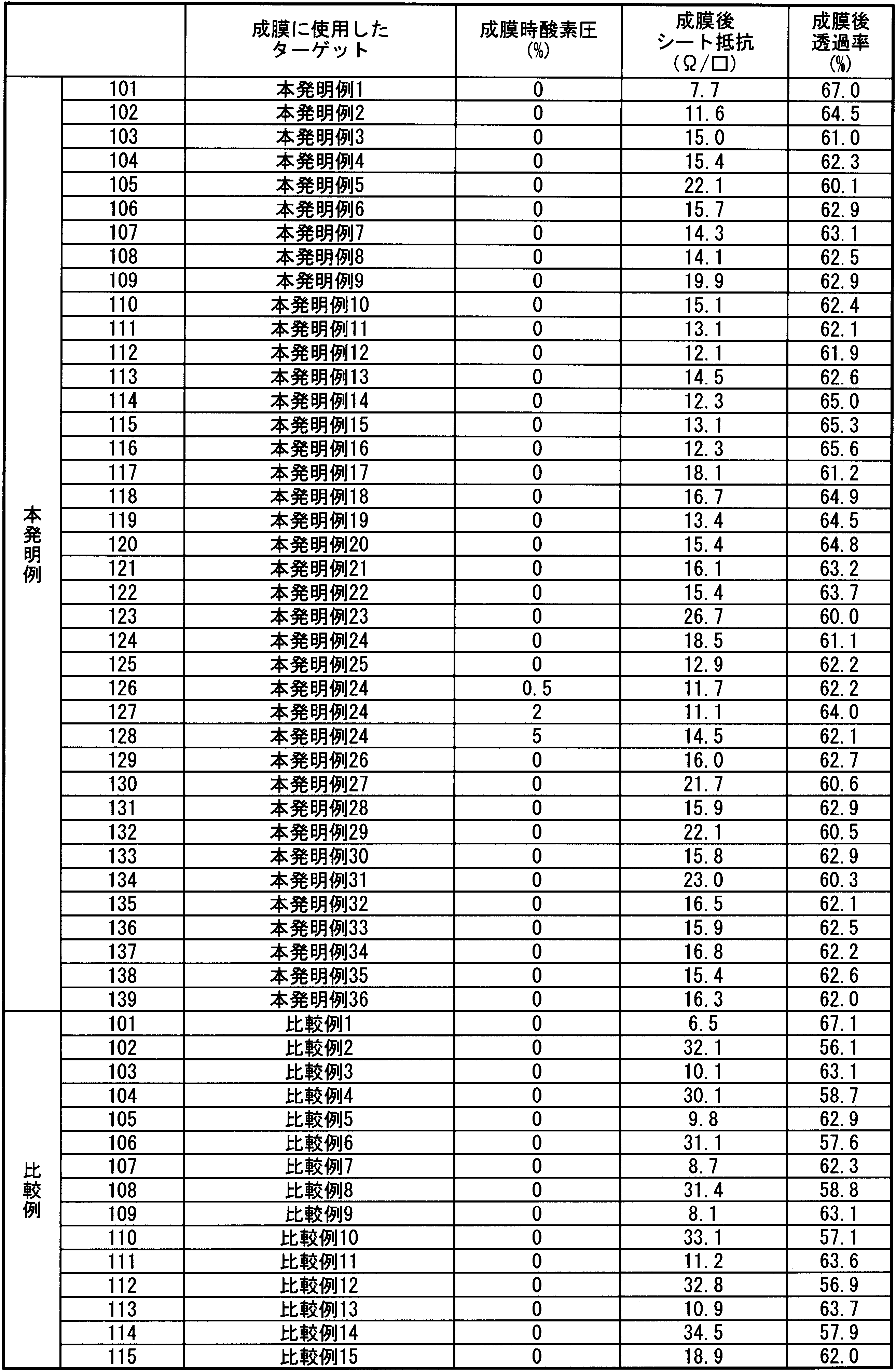
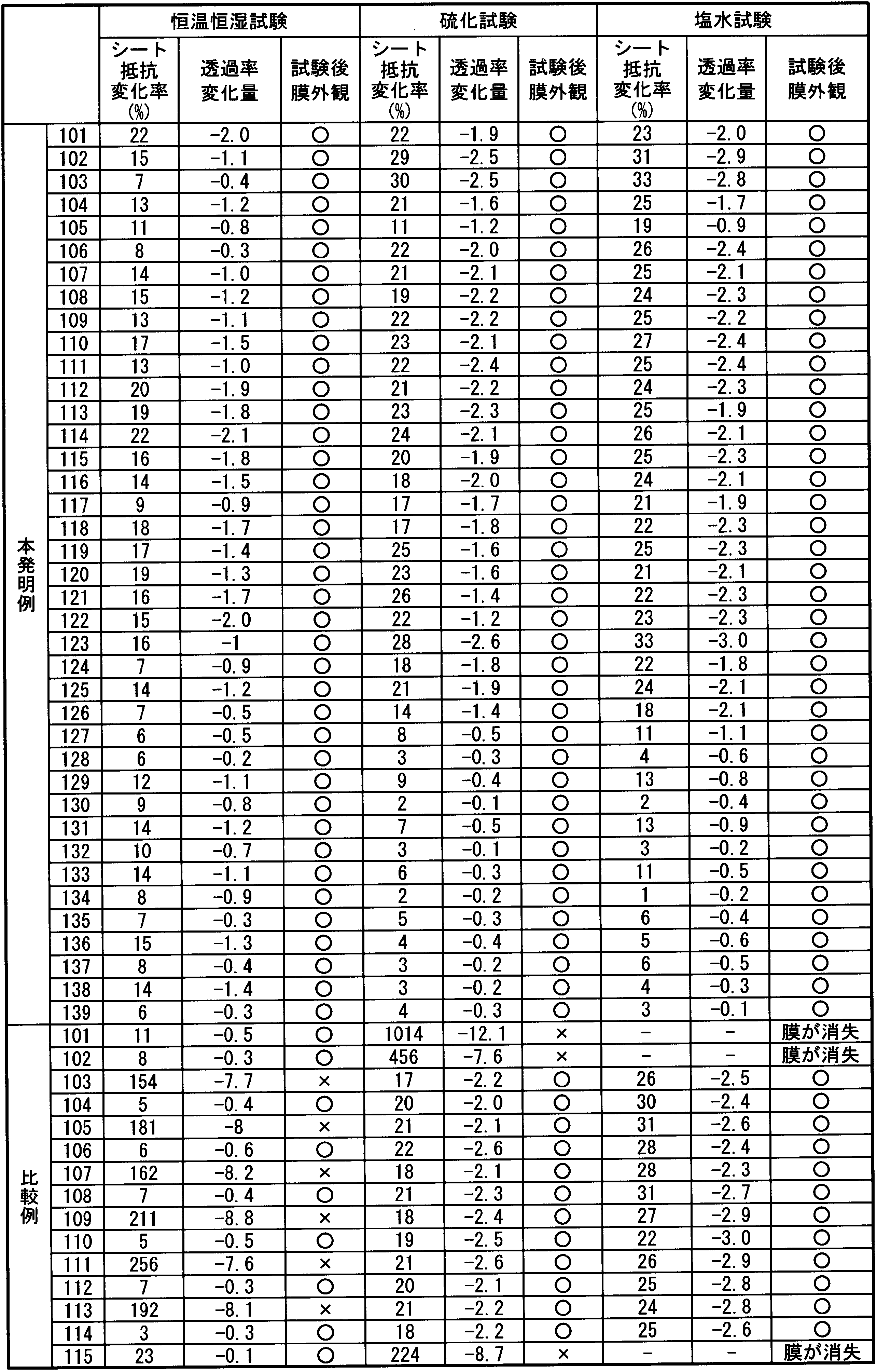
Tiの含有量が0.1原子%よりも少ないAg合金スパッタリングターゲット(比較例1)を用いた比較例101においては、硫化試験の前後でシート抵抗が大きく増加し、透過率が大きく低下し、硫化試験後のAg合金膜には変色・斑点等が発生していた。さらに、塩水試験後は、Ag合金膜が消失していた。
Tiの含有量が5.0原子%よりも多いAg合金スパッタリングターゲット(比較例2)を用いた比較例102においては、硫化試験の前後でシート抵抗が大きく増加し、透過率が大きく低下し、硫化試験後のAg合金膜には変色・斑点等が発生していた。さらに、塩水試験後は、Ag合金膜が消失していた。
Cu、Sn、Mg、In、Sb、Al、Zn、Ge、Gaの合計含有量が0.1原子%よりも少ないAg合金スパッタリングターゲット(比較例3、5、7、9、11、13)を用いた比較例103、105、107、109、111、113においては、恒温恒湿試験の前後でシート抵抗が大きく増加し、透過率が大きく低下し、恒温恒湿試験後のAg合金膜には変色・斑点等が発生していた。
Cu、Sn、Mg、In、Sb、Al、Zn、Ge、Gaの合計含有量がTiとの総計で10.0原子%より多いAg合金スパッタリングターゲット(比較例4、6、8、10、12、14)を用いた比較例104、106、108、110、112、114においては、成膜後のシート抵抗が30Ω/□(Ω/sq.)を超えて大きく、かつ透過率が60%よりも低かった。
Na、Si、V、Cr、Fe、Coの合計含有量が100質量ppmよりも多いAg合金スパッタリングターゲット(比較例15)を用いた比較例115においては、硫化試験の前後でシート抵抗が大きく増加し、透過率が大きく低下し、硫化試験後のAg合金膜には変色・斑点等が発生していた。さらに、塩水試験後は、Ag合金膜が消失していた。
これに対して、Tiを0.1原子%以上5.0原子%以下の範囲で含有し、Cu、Sn、Mg、In、Sb、Al、Zn、Ge、Gaから選ばれる少なくとも1種の元素を合計で0.1原子%以上かつTiとの総計で10.0原子%以下となる範囲で含有し、さらにNa、Si、V、Cr、Fe、Coの合計含有量が100質量ppm以下であるAg合金スパッタリングターゲット(本発明例1~25)を用いた本発明例101~128においてはいずれも、成膜後のシート抵抗が30Ω/□よりも小さく、かつ透過率が60%を超えていた。また、恒温恒湿試験、硫化試験、塩水試験のいずれの試験においても試験の前後でシート抵抗及び透過率は大きく変化せず、さらに試験後のAg合金膜には変色・斑点等が発生せずに安定していた。
特に、Arと酸素との混合ガス雰囲気中にて成膜を行った本発明例126~128においては、同じAg合金スパッタリングターゲットを用いてArガス雰囲気中にて成膜を行った本発明例124と比較して、成膜後のシート抵抗が小さく、かつ透過率が高く、さらに、恒温恒湿試験、硫化試験、塩水試験のいずれの試験においても概ねシート抵抗及び透過率の変化が小さく、耐腐食性が向上した。
また、Pd、Pt、Auから選ばれる少なくとも1種の元素を合計で0.1原子%以上かつTi、Cu、Sn、Mg、In、Sb、Al、Zn、Ge、Gaとの総計で10.0原子%以下となる範囲で含有するAg合金スパッタリングターゲット(本発明例26~36)を用いた本発明例129~139においては、硫化試験と塩水試験の前後でのシート抵抗及び透過率の変化が概ね小さくなった。
以上のことから、本発明によれば、抵抗が低く、かつ透過率が高く、さらに、耐熱性、耐湿性、耐硫黄性、耐塩素性に優れ、半透明電極膜として適したAg合金膜を提供可能であることが確認された。
実施例3:Ag合金膜(反射膜)の作製
[本発明例140~141、比較例116~117]
実施例1で作製したAg合金スパッタリングターゲットをスパッタ装置に装着し、実施例2と同じ条件でスパッタリングを実施して、ガラス基板の表面に厚さ100nmのAg合金膜を成膜し、実施例2と同様の手順でAg合金膜を評価した。その内容を表5に示す。
ここで、表5の「成膜後反射率」は、得られたAg合金膜の反射率を分光光度計を用いて測定した値である。なお、表に示している数値は波長550nmの光の反射率である。また、「反射率変化量」は、波長550nmにおける反射率の変化量[=各試験後の透過率-成膜後透過率]である。
[本発明例140~141、比較例116~117]
実施例1で作製したAg合金スパッタリングターゲットをスパッタ装置に装着し、実施例2と同じ条件でスパッタリングを実施して、ガラス基板の表面に厚さ100nmのAg合金膜を成膜し、実施例2と同様の手順でAg合金膜を評価した。その内容を表5に示す。
ここで、表5の「成膜後反射率」は、得られたAg合金膜の反射率を分光光度計を用いて測定した値である。なお、表に示している数値は波長550nmの光の反射率である。また、「反射率変化量」は、波長550nmにおける反射率の変化量[=各試験後の透過率-成膜後透過率]である。

Tiの含有量が0.1原子%よりも少ないAg合金スパッタリングターゲット(比較例1)を用いた比較例116においては、硫化試験の前後でシート抵抗が大きく増加し、反射率が大きく低下し、硫化試験後のAg合金膜には変色・斑点等が発生していた。さらに、塩水試験後は、Ag合金膜が消失していた。
Tiの含有量が5.0原子%よりも多いAg合金スパッタリングターゲット(比較例2)を用いた比較例117においては、硫化試験の前後でシート抵抗が大きく増加し、反射率が大きく低下し、硫化試験後のAg合金膜には変色・斑点等が発生していた。さらに、塩水試験後は、Ag合金膜が消失していた。
これに対して、Tiを0.1原子%以上5.0原子%以下の範囲で含有し、Cu、Sn、Mg、In、Sb、Al、Zn、Ge、Gaから選ばれる少なくとも1種の元素を合計で0.1原子%以上かつTiとの総計で10.0原子%以下となる範囲で含有し、さらにNa、Si、V、Cr、Fe、Coの合計含有量が100質量ppm以下であるAg合金スパッタリングターゲット(本発明例24)を用いた本発明例140においては、恒温恒湿試験、硫化試験、塩水試験のいずれの試験においても試験の前後でシート抵抗及び反射率は大きく変化せず、さらに試験後のAg合金膜には変色・斑点等が発生せずに安定していた。
特に、Arと酸素との混合ガス雰囲気中にて成膜を行った本発明例141においては、同じAg合金スパッタリングターゲットを用いてArガス雰囲気中にて成膜を行った本発明例140と比較して、恒温恒湿試験、硫化試験、塩水試験のいずれの試験においてもシート抵抗及び透過率の変化が小さく、耐腐食性が向上した。
以上のことから、本発明によれば、抵抗が低く、かつ透過率が高く、さらに、耐熱性、耐湿性、耐硫黄性、耐塩素性に優れ、反射電極膜として適したAg合金膜を提供可能であることが確認された。
実施例4:半透明導電積層膜(導電性酸化物膜/Ag合金膜/導電性酸化物膜)の作製[本発明例201~217、比較例201~208]
実施例1で作製したAg合金スパッタリングターゲットと下記の導電性酸化物成膜用ターゲットをスパッタ装置に装着し、実施例2と同じ条件でスパッタリングを実施して、ガラス基板の表面に厚さ20nmの導電性酸化物(A)の膜と、厚さ10nmのAg合金の膜(半透明膜)と厚さ20nmの導電性酸化物(B)の膜をこの順で積層した半透明導電積層膜を成膜し、実施例2のAg合金膜の評価と同様に半透明導電積層膜を評価した。その内容を表6,7に示す。
(導電性酸化物成膜用ターゲットの組成)
ITO:酸化インジウム90mol%、酸化錫10mol%
IZO:酸化インジウム70mol%、酸化亜鉛30mol%
AZO:酸化アルミニウム2mol%、酸化亜鉛98mol%
GZO:酸化ガリウム2mol%、酸化亜鉛98mol%
なお、導電性酸化物膜は2%の酸素を含有するArガス雰囲気で成膜した。
実施例1で作製したAg合金スパッタリングターゲットと下記の導電性酸化物成膜用ターゲットをスパッタ装置に装着し、実施例2と同じ条件でスパッタリングを実施して、ガラス基板の表面に厚さ20nmの導電性酸化物(A)の膜と、厚さ10nmのAg合金の膜(半透明膜)と厚さ20nmの導電性酸化物(B)の膜をこの順で積層した半透明導電積層膜を成膜し、実施例2のAg合金膜の評価と同様に半透明導電積層膜を評価した。その内容を表6,7に示す。
(導電性酸化物成膜用ターゲットの組成)
ITO:酸化インジウム90mol%、酸化錫10mol%
IZO:酸化インジウム70mol%、酸化亜鉛30mol%
AZO:酸化アルミニウム2mol%、酸化亜鉛98mol%
GZO:酸化ガリウム2mol%、酸化亜鉛98mol%
なお、導電性酸化物膜は2%の酸素を含有するArガス雰囲気で成膜した。


Tiの含有量が0.1原子%よりも少ないAg合金スパッタリングターゲット(比較例1)を用いた比較例201、203、205、207においては、導電性酸化物(A)、(B)がいずれであっても、硫化試験の前後でシート抵抗が大きく増加し、透過率が大きく低下し、硫化試験後のAg合金膜の縁が変色していた。さらに、塩水試験後は、Ag合金膜が消失していた。
Tiの含有量が5.0原子%よりも多いAg合金スパッタリングターゲット(比較例2)を用いた比較例202、204、206、208においては、導電性酸化物(A)、(B)がいずれであっても、成膜後のシート抵抗が30Ω/□を超えて大きく、かつ透過率が80%よりも低かった。また、硫化試験の前後でシート抵抗が大きく増加し、透過率が大きく低下し、硫化試験後のAg合金膜の縁が変色していた。さらに、塩水試験後は、Ag合金膜が消失していた。
これに対して、Tiを0.1原子%以上5.0原子%以下の範囲で含有し、Cu、Sn、Mg、In、Sb、Al、Zn、Ge、Gaから選ばれる少なくとも1種の元素を合計で0.1原子%以上かつTiとの総計で10.0原子%以下となる範囲で含有し、さらにNa、Si、V、Cr、Fe、Coの合計含有量が100質量ppm以下であるAg合金スパッタリングターゲット(本発明例2,4,5,14,15,23,25)を用いた本発明例201~216においては、いずれにおいても、成膜後のシート抵抗が30Ω/□よりも小さく、かつ透過率が80%を超えていた。また、恒温恒湿試験、硫化試験、塩水試験のいずれの試験においても試験の前後でシート抵抗及び透過率は大きく変化せず、さらに試験後の積層膜には変色・斑点等が発生せずに安定していた。
特に、Arと酸素との混合ガス雰囲気中にて成膜を行った本発明例208~210においては、同じAg合金スパッタリングターゲットを用いてArガス雰囲気中にて成膜を行った本発明例204と比較して、成膜後シート抵抗が低く、成膜後透過率が概ね高く、また、恒温恒湿試験、硫化試験、塩水試験のいずれの試験においてもシート抵抗及び透過率の変化が概ね小さく、安定性が向上した。
また、Pdを含有するAg合金スパッタリングターゲット(本発明例27)を用いた本発明例217においては、硫化試験と塩水試験の前後でのシート抵抗及び透過率の変化が概ね小さくなった。
以上のことから、本発明によるAg合金膜は、導電性酸化物膜との半透明導電積層膜として利用しても、腐食が促進されにくく、安定であることが確認された。
実施例5:反射導電積層膜(導電性酸化物膜/Ag合金膜/導電性酸化物膜)の作製[本発明例218~219、比較例209~210]
実施例1で作製したAg合金スパッタリングターゲットと下記の導電性酸化物成膜用ターゲットをスパッタ装置に装着し、実施例4と同じ条件でスパッタリングを実施して、ガラス基板の表面に厚さ20nmの導電性酸化物(A)の膜と、厚さ100nmのAg合金の膜(反射膜)と厚さ20nmの導電性酸化物(B)の膜をこの順で積層した反射導電積層膜を作成し、実施例3のAg合金膜の評価と同様に反射導電積層膜を評価した。その内容を表8に示す。
実施例1で作製したAg合金スパッタリングターゲットと下記の導電性酸化物成膜用ターゲットをスパッタ装置に装着し、実施例4と同じ条件でスパッタリングを実施して、ガラス基板の表面に厚さ20nmの導電性酸化物(A)の膜と、厚さ100nmのAg合金の膜(反射膜)と厚さ20nmの導電性酸化物(B)の膜をこの順で積層した反射導電積層膜を作成し、実施例3のAg合金膜の評価と同様に反射導電積層膜を評価した。その内容を表8に示す。

Tiの含有量が0.1原子%よりも少ないAg合金スパッタリングターゲット(比較例1)を用いた比較例209は、硫化試験の前後でシート抵抗が増加し、反射率が低下し、硫化試験後のAg合金膜の縁が変色していた。さらに、塩水試験後は、Ag合金膜が消失していた。
Tiの含有量が5.0原子%よりも多いAg合金スパッタリングターゲット(比較例2)を用いた比較例210においては、成膜後シート抵抗が大きく、かつ反射率が低かった。また、硫化試験の前後でシート抵抗が増加し、反射率が低下し、硫化試験後のAg合金膜の縁が変色していた。さらに、塩水試験後は、Ag合金膜が消失していた。
これに対して、Tiを0.1原子%以上5.0原子%以下の範囲で含有し、Cu、Sn、Mg、In、Sb、Al、Zn、Ge、Gaから選ばれる少なくとも1種の元素を合計で0.1原子%以上かつTiとの総計で10.0原子%以下となる範囲で含有し、さらにNa、Si、V、Cr、Fe、Coの合計含有量が100質量ppm以下であるAg合金スパッタリングターゲット(本発明例14)を用いた本発明例218、219においては、成膜後シート抵抗が小さく、かつ反射率は94%を超えていた。さらに、恒温恒湿試験、硫化試験、塩水試験のいずれの試験においても試験の前後でシート抵抗及び透過率は大きく変化せず、さらに試験後のAg合金膜には変色・斑点等が発生せずに安定していた。
以上のことから、本発明によるAg合金膜は、導電性酸化物膜と積層した反射導電積層膜として利用しても、腐食が促進されにくく、安定であることが確認された。
本発明のAg合金膜は、成膜直後は優れた光学特性と導電性とを有し、かつ、熱湿環境下においてもその光学特性と導電性とが大きく変化することがなく、塩素や硫黄による腐食がおこりにくく、さらに超薄膜にしても凝集が起こりにくいので、反射電極膜や半透明電極膜に好適である。
Claims (13)
- Tiを0.1原子%以上5.0原子%以下、Cu、Sn、Mg、In、Sb、Al、Zn、Ge、Gaから選ばれる少なくとも1種の元素を合計で0.1原子%以上かつTiとの総計で10.0原子%以下となる範囲で含有し、残部がAgと不可避不純物からなり、Na、Si、V、Cr、Fe、Coの合計含有量が100質量ppm以下であることを特徴とするAg合金膜。
- Tiの含有量Aと、Cu、Sn、Mg、In、Sb、Al、Zn、Ge、Gaの合計含有量Bとの原子比A/Bが、0.1以上6.0以下の範囲にあることを特徴とする請求項1に記載のAg合金膜。
- さらに、Pd、Pt、Auから選ばれる少なくとも1種の元素を合計で0.1原子%以上かつTi、Cu、Sn、Mg、In、Sb、Al、Zn、Ge、Gaとの総計で10.0原子%以下となる範囲で含有することを特徴とする請求項1又は請求項2に記載のAg合金膜。
- 膜厚が20nm以下であることを特徴とする請求項1から請求項3のいずれか一項に記載のAg合金膜。
- 請求項1から請求項4のいずれか一項に記載のAg合金膜と、該Ag合金膜の片面または両面に形成された導電性酸化物膜と、を備えることを特徴とする積層膜。
- Tiを0.1原子%以上5.0原子%以下、Cu、Sn、Mg、In、Sb、Al、Zn、Ge、Gaから選ばれる少なくとも1種の元素を合計で0.1原子%以上かつTiとの総計が10.0原子%以下となる範囲で含有し、残部がAgと不可避不純物からなり、Na、Si、V、Cr、Fe、Coの合計含有量が100質量ppm以下であることを特徴とするAg合金スパッタリングターゲット。
- Tiの含有量Aと、Cu、Sn、Mg、In、Sb、Al、Zn、Ge、Gaの合計含有量Bとの原子比A/Bが、0.1以上6.0以下の範囲にあることを特徴とする請求項6に記載のAg合金スパッタリングターゲット。
- さらに、Pd、Pt、Auから選ばれる少なくとも1種の元素を合計で0.1原子%以上かつTi、Cu、Sn、Mg、In、Sb、Al、Zn、Ge、Gaとの総計で10.0原子%以下となる範囲で含有することを特徴とする請求項6又は請求項7に記載のAg合金スパッタリングターゲット。
- 前記Na、Si、V、Cr、Fe、Coの合計含有量が10質量ppm以下であることを特徴とする請求項6から請求項8のいずれかの一項に記載のAg合金スパッタリングターゲット。
- 複数のAg合金結晶を含む多結晶体であって、前記Ag合金結晶の粒径を複数の箇所において測定した結果、測定した全てのAg合金結晶の粒径の平均値である平均結晶粒径Cと、測定した各箇所でのAg合金結晶の粒径の平均値Dのうち、前記平均結晶粒径Cの偏差の絶対値が最大となる平均値Dmaxとから定義されるAg合金結晶粒径のばらつきE(%)=(Dmax-C)/C×100が20%以内であることを特徴とする請求項6から請求項9のいずれか一項に記載のAg合金スパッタリングターゲット。
- 前記平均結晶粒径Cが、200μm以下であることを特徴とする請求項10に記載のAg合金スパッタリングターゲット。
- 請求項6から請求項11のいずれか一項に記載のAg合金スパッタリングターゲットを用いてスパッタリングを行うことを特徴とするAg合金膜の製造方法。
- 不活性ガスの全圧に対して0.5~5%の圧力となる量の酸素を含むガス雰囲気にてスパッタリングを行うことを特徴とする請求項12に記載のAg合金膜の製造方法。
Priority Applications (2)
| Application Number | Priority Date | Filing Date | Title |
|---|---|---|---|
| KR1020177036899A KR20180034334A (ko) | 2015-07-28 | 2016-07-21 | Ag 합금막과 그 제조 방법, Ag 합금 스퍼터링 타겟 및 적층막 |
| CN201680038273.2A CN107709584B (zh) | 2015-07-28 | 2016-07-21 | Ag合金膜及其制造方法、Ag合金溅射靶以及层叠膜 |
Applications Claiming Priority (4)
| Application Number | Priority Date | Filing Date | Title |
|---|---|---|---|
| JP2015-148474 | 2015-07-28 | ||
| JP2015148474 | 2015-07-28 | ||
| JP2016131593A JP6801264B2 (ja) | 2015-07-28 | 2016-07-01 | Ag合金膜とその製造方法、Ag合金スパッタリングターゲットおよび積層膜 |
| JP2016-131593 | 2016-07-01 |
Publications (1)
| Publication Number | Publication Date |
|---|---|
| WO2017018310A1 true WO2017018310A1 (ja) | 2017-02-02 |
Family
ID=57884782
Family Applications (1)
| Application Number | Title | Priority Date | Filing Date |
|---|---|---|---|
| PCT/JP2016/071375 Ceased WO2017018310A1 (ja) | 2015-07-28 | 2016-07-21 | Ag合金膜とその製造方法、Ag合金スパッタリングターゲットおよび積層膜 |
Country Status (1)
| Country | Link |
|---|---|
| WO (1) | WO2017018310A1 (ja) |
Cited By (1)
| Publication number | Priority date | Publication date | Assignee | Title |
|---|---|---|---|---|
| JP2018176493A (ja) * | 2017-04-07 | 2018-11-15 | 三菱マテリアル株式会社 | 積層膜、及び、Ag合金スパッタリングターゲット |
Citations (5)
| Publication number | Priority date | Publication date | Assignee | Title |
|---|---|---|---|---|
| JP2003055721A (ja) * | 2001-08-09 | 2003-02-26 | Ulvac Japan Ltd | Ag合金薄膜電極、有機EL素子及びスパッタリング用ターゲット |
| JP2004043868A (ja) * | 2002-07-10 | 2004-02-12 | Hitachi Metals Ltd | 薄膜形成用スパッタリングターゲット材及びその製造方法 |
| WO2006132415A1 (ja) * | 2005-06-10 | 2006-12-14 | Tanaka Kikinzoku Kogyo K.K. | 反射率・透過率維持特性に優れた銀合金 |
| JP2014139339A (ja) * | 2012-12-21 | 2014-07-31 | Mitsubishi Materials Corp | Ag合金スパッタリングターゲット |
| JP2016065308A (ja) * | 2014-09-18 | 2016-04-28 | 三菱マテリアル株式会社 | Ag合金スパッタリングターゲット、Ag合金スパッタリングターゲットの製造方法、Ag合金膜およびAg合金膜の製造方法 |
-
2016
- 2016-07-21 WO PCT/JP2016/071375 patent/WO2017018310A1/ja not_active Ceased
Patent Citations (5)
| Publication number | Priority date | Publication date | Assignee | Title |
|---|---|---|---|---|
| JP2003055721A (ja) * | 2001-08-09 | 2003-02-26 | Ulvac Japan Ltd | Ag合金薄膜電極、有機EL素子及びスパッタリング用ターゲット |
| JP2004043868A (ja) * | 2002-07-10 | 2004-02-12 | Hitachi Metals Ltd | 薄膜形成用スパッタリングターゲット材及びその製造方法 |
| WO2006132415A1 (ja) * | 2005-06-10 | 2006-12-14 | Tanaka Kikinzoku Kogyo K.K. | 反射率・透過率維持特性に優れた銀合金 |
| JP2014139339A (ja) * | 2012-12-21 | 2014-07-31 | Mitsubishi Materials Corp | Ag合金スパッタリングターゲット |
| JP2016065308A (ja) * | 2014-09-18 | 2016-04-28 | 三菱マテリアル株式会社 | Ag合金スパッタリングターゲット、Ag合金スパッタリングターゲットの製造方法、Ag合金膜およびAg合金膜の製造方法 |
Cited By (1)
| Publication number | Priority date | Publication date | Assignee | Title |
|---|---|---|---|---|
| JP2018176493A (ja) * | 2017-04-07 | 2018-11-15 | 三菱マテリアル株式会社 | 積層膜、及び、Ag合金スパッタリングターゲット |
Similar Documents
| Publication | Publication Date | Title |
|---|---|---|
| CN107709584B (zh) | Ag合金膜及其制造方法、Ag合金溅射靶以及层叠膜 | |
| JP6278136B2 (ja) | Ag合金スパッタリングターゲット、Ag合金スパッタリングターゲットの製造方法およびAg合金膜の製造方法 | |
| KR101854009B1 (ko) | 도전성 막 형성용 은 합금 스퍼터링 타겟 및 그 제조 방법 | |
| KR101679562B1 (ko) | 도전성 막 형성용 은 합금 조성물 및 이의 제조 방법 | |
| JP2022008503A (ja) | 積層膜、及び、Ag合金スパッタリングターゲット | |
| WO2016043183A1 (ja) | Ag合金スパッタリングターゲット、Ag合金スパッタリングターゲットの製造方法、Ag合金膜およびAg合金膜の製造方法 | |
| WO2017018310A1 (ja) | Ag合金膜とその製造方法、Ag合金スパッタリングターゲットおよび積層膜 | |
| JP6729344B2 (ja) | Ag合金スパッタリングターゲットおよびAg合金膜 | |
| JP6853458B2 (ja) | Ag合金スパッタリングターゲット、及び、Ag合金膜 | |
| WO2020070824A1 (ja) | 積層膜、及び、Ag合金スパッタリングターゲット | |
| TW202041683A (zh) | 銀合金濺鍍靶及銀合金膜 | |
| JP2015061931A (ja) | Ag合金膜、Ag合金導電膜、Ag合金反射膜、Ag合金半透過膜およびAg合金膜形成用スパッタリングターゲット | |
| WO2021090581A1 (ja) | Ag合金スパッタリングターゲット、及び、Ag合金膜 | |
| TW201631168A (zh) | 銅基合金濺鍍靶材 | |
| JP2016153525A (ja) | スパッタリングターゲット、及び、積層膜 |
Legal Events
| Date | Code | Title | Description |
|---|---|---|---|
| 121 | Ep: the epo has been informed by wipo that ep was designated in this application |
Ref document number: 16830415 Country of ref document: EP Kind code of ref document: A1 |
|
| ENP | Entry into the national phase |
Ref document number: 20177036899 Country of ref document: KR Kind code of ref document: A |
|
| NENP | Non-entry into the national phase |
Ref country code: DE |
|
| 122 | Ep: pct application non-entry in european phase |
Ref document number: 16830415 Country of ref document: EP Kind code of ref document: A1 |