WO2017018017A1 - 発光素子 - Google Patents
発光素子 Download PDFInfo
- Publication number
- WO2017018017A1 WO2017018017A1 PCT/JP2016/063944 JP2016063944W WO2017018017A1 WO 2017018017 A1 WO2017018017 A1 WO 2017018017A1 JP 2016063944 W JP2016063944 W JP 2016063944W WO 2017018017 A1 WO2017018017 A1 WO 2017018017A1
- Authority
- WO
- WIPO (PCT)
- Prior art keywords
- region
- compound semiconductor
- light
- injection
- mode loss
- Prior art date
Links
Images


Classifications
-
- H—ELECTRICITY
- H01—ELECTRIC ELEMENTS
- H01S—DEVICES USING THE PROCESS OF LIGHT AMPLIFICATION BY STIMULATED EMISSION OF RADIATION [LASER] TO AMPLIFY OR GENERATE LIGHT; DEVICES USING STIMULATED EMISSION OF ELECTROMAGNETIC RADIATION IN WAVE RANGES OTHER THAN OPTICAL
- H01S5/00—Semiconductor lasers
- H01S5/10—Construction or shape of the optical resonator, e.g. extended or external cavity, coupled cavities, bent-guide, varying width, thickness or composition of the active region
- H01S5/18—Surface-emitting [SE] lasers, e.g. having both horizontal and vertical cavities
- H01S5/183—Surface-emitting [SE] lasers, e.g. having both horizontal and vertical cavities having only vertical cavities, e.g. vertical cavity surface-emitting lasers [VCSEL]
- H01S5/18308—Surface-emitting [SE] lasers, e.g. having both horizontal and vertical cavities having only vertical cavities, e.g. vertical cavity surface-emitting lasers [VCSEL] having a special structure for lateral current or light confinement
-
- H—ELECTRICITY
- H01—ELECTRIC ELEMENTS
- H01S—DEVICES USING THE PROCESS OF LIGHT AMPLIFICATION BY STIMULATED EMISSION OF RADIATION [LASER] TO AMPLIFY OR GENERATE LIGHT; DEVICES USING STIMULATED EMISSION OF ELECTROMAGNETIC RADIATION IN WAVE RANGES OTHER THAN OPTICAL
- H01S5/00—Semiconductor lasers
- H01S5/02—Structural details or components not essential to laser action
- H01S5/028—Coatings ; Treatment of the laser facets, e.g. etching, passivation layers or reflecting layers
-
- H—ELECTRICITY
- H01—ELECTRIC ELEMENTS
- H01S—DEVICES USING THE PROCESS OF LIGHT AMPLIFICATION BY STIMULATED EMISSION OF RADIATION [LASER] TO AMPLIFY OR GENERATE LIGHT; DEVICES USING STIMULATED EMISSION OF ELECTROMAGNETIC RADIATION IN WAVE RANGES OTHER THAN OPTICAL
- H01S5/00—Semiconductor lasers
- H01S5/04—Processes or apparatus for excitation, e.g. pumping, e.g. by electron beams
- H01S5/042—Electrical excitation ; Circuits therefor
- H01S5/0421—Electrical excitation ; Circuits therefor characterised by the semiconducting contacting layers
-
- H—ELECTRICITY
- H01—ELECTRIC ELEMENTS
- H01S—DEVICES USING THE PROCESS OF LIGHT AMPLIFICATION BY STIMULATED EMISSION OF RADIATION [LASER] TO AMPLIFY OR GENERATE LIGHT; DEVICES USING STIMULATED EMISSION OF ELECTROMAGNETIC RADIATION IN WAVE RANGES OTHER THAN OPTICAL
- H01S5/00—Semiconductor lasers
- H01S5/04—Processes or apparatus for excitation, e.g. pumping, e.g. by electron beams
- H01S5/042—Electrical excitation ; Circuits therefor
- H01S5/0425—Electrodes, e.g. characterised by the structure
- H01S5/04252—Electrodes, e.g. characterised by the structure characterised by the material
- H01S5/04253—Electrodes, e.g. characterised by the structure characterised by the material having specific optical properties, e.g. transparent electrodes
-
- H—ELECTRICITY
- H01—ELECTRIC ELEMENTS
- H01S—DEVICES USING THE PROCESS OF LIGHT AMPLIFICATION BY STIMULATED EMISSION OF RADIATION [LASER] TO AMPLIFY OR GENERATE LIGHT; DEVICES USING STIMULATED EMISSION OF ELECTROMAGNETIC RADIATION IN WAVE RANGES OTHER THAN OPTICAL
- H01S5/00—Semiconductor lasers
- H01S5/10—Construction or shape of the optical resonator, e.g. extended or external cavity, coupled cavities, bent-guide, varying width, thickness or composition of the active region
- H01S5/18—Surface-emitting [SE] lasers, e.g. having both horizontal and vertical cavities
- H01S5/183—Surface-emitting [SE] lasers, e.g. having both horizontal and vertical cavities having only vertical cavities, e.g. vertical cavity surface-emitting lasers [VCSEL]
- H01S5/18361—Structure of the reflectors, e.g. hybrid mirrors
- H01S5/18369—Structure of the reflectors, e.g. hybrid mirrors based on dielectric materials
-
- H—ELECTRICITY
- H01—ELECTRIC ELEMENTS
- H01S—DEVICES USING THE PROCESS OF LIGHT AMPLIFICATION BY STIMULATED EMISSION OF RADIATION [LASER] TO AMPLIFY OR GENERATE LIGHT; DEVICES USING STIMULATED EMISSION OF ELECTROMAGNETIC RADIATION IN WAVE RANGES OTHER THAN OPTICAL
- H01S5/00—Semiconductor lasers
- H01S5/10—Construction or shape of the optical resonator, e.g. extended or external cavity, coupled cavities, bent-guide, varying width, thickness or composition of the active region
- H01S5/18—Surface-emitting [SE] lasers, e.g. having both horizontal and vertical cavities
- H01S5/183—Surface-emitting [SE] lasers, e.g. having both horizontal and vertical cavities having only vertical cavities, e.g. vertical cavity surface-emitting lasers [VCSEL]
- H01S5/18386—Details of the emission surface for influencing the near- or far-field, e.g. a grating on the surface
- H01S5/18391—Aperiodic structuring to influence the near- or far-field distribution
-
- H—ELECTRICITY
- H01—ELECTRIC ELEMENTS
- H01S—DEVICES USING THE PROCESS OF LIGHT AMPLIFICATION BY STIMULATED EMISSION OF RADIATION [LASER] TO AMPLIFY OR GENERATE LIGHT; DEVICES USING STIMULATED EMISSION OF ELECTROMAGNETIC RADIATION IN WAVE RANGES OTHER THAN OPTICAL
- H01S5/00—Semiconductor lasers
- H01S5/20—Structure or shape of the semiconductor body to guide the optical wave ; Confining structures perpendicular to the optical axis, e.g. index or gain guiding, stripe geometry, broad area lasers, gain tailoring, transverse or lateral reflectors, special cladding structures, MQW barrier reflection layers
- H01S5/2004—Confining in the direction perpendicular to the layer structure
-
- H—ELECTRICITY
- H01—ELECTRIC ELEMENTS
- H01S—DEVICES USING THE PROCESS OF LIGHT AMPLIFICATION BY STIMULATED EMISSION OF RADIATION [LASER] TO AMPLIFY OR GENERATE LIGHT; DEVICES USING STIMULATED EMISSION OF ELECTROMAGNETIC RADIATION IN WAVE RANGES OTHER THAN OPTICAL
- H01S5/00—Semiconductor lasers
- H01S5/04—Processes or apparatus for excitation, e.g. pumping, e.g. by electron beams
- H01S5/042—Electrical excitation ; Circuits therefor
- H01S5/0425—Electrodes, e.g. characterised by the structure
- H01S5/04252—Electrodes, e.g. characterised by the structure characterised by the material
-
- H—ELECTRICITY
- H01—ELECTRIC ELEMENTS
- H01S—DEVICES USING THE PROCESS OF LIGHT AMPLIFICATION BY STIMULATED EMISSION OF RADIATION [LASER] TO AMPLIFY OR GENERATE LIGHT; DEVICES USING STIMULATED EMISSION OF ELECTROMAGNETIC RADIATION IN WAVE RANGES OTHER THAN OPTICAL
- H01S5/00—Semiconductor lasers
- H01S5/10—Construction or shape of the optical resonator, e.g. extended or external cavity, coupled cavities, bent-guide, varying width, thickness or composition of the active region
- H01S5/18—Surface-emitting [SE] lasers, e.g. having both horizontal and vertical cavities
- H01S5/183—Surface-emitting [SE] lasers, e.g. having both horizontal and vertical cavities having only vertical cavities, e.g. vertical cavity surface-emitting lasers [VCSEL]
- H01S5/18341—Intra-cavity contacts
-
- H—ELECTRICITY
- H01—ELECTRIC ELEMENTS
- H01S—DEVICES USING THE PROCESS OF LIGHT AMPLIFICATION BY STIMULATED EMISSION OF RADIATION [LASER] TO AMPLIFY OR GENERATE LIGHT; DEVICES USING STIMULATED EMISSION OF ELECTROMAGNETIC RADIATION IN WAVE RANGES OTHER THAN OPTICAL
- H01S5/00—Semiconductor lasers
- H01S5/30—Structure or shape of the active region; Materials used for the active region
- H01S5/34—Structure or shape of the active region; Materials used for the active region comprising quantum well or superlattice structures, e.g. single quantum well [SQW] lasers, multiple quantum well [MQW] lasers or graded index separate confinement heterostructure [GRINSCH] lasers
- H01S5/343—Structure or shape of the active region; Materials used for the active region comprising quantum well or superlattice structures, e.g. single quantum well [SQW] lasers, multiple quantum well [MQW] lasers or graded index separate confinement heterostructure [GRINSCH] lasers in AIIIBV compounds, e.g. AlGaAs-laser, InP-based laser
- H01S5/34333—Structure or shape of the active region; Materials used for the active region comprising quantum well or superlattice structures, e.g. single quantum well [SQW] lasers, multiple quantum well [MQW] lasers or graded index separate confinement heterostructure [GRINSCH] lasers in AIIIBV compounds, e.g. AlGaAs-laser, InP-based laser with a well layer based on Ga(In)N or Ga(In)P, e.g. blue laser
Definitions
- the present disclosure relates to a light emitting device (specifically, a vertical cavity laser, a surface emitting laser device also referred to as a VCSEL).
- a light emitting device specifically, a vertical cavity laser, a surface emitting laser device also referred to as a VCSEL.
- a light-emitting element composed of a surface-emitting laser element laser oscillation generally occurs when laser light is resonated between two light reflecting layers (Distributed Bragg Reflector layer or DBR layer).
- DBR layer distributed Bragg Reflector layer
- a surface emitting laser device having a structure in which an n-type GaN compound semiconductor layer, an active layer (light emitting layer) made of a GaN compound semiconductor, and a p-type GaN compound semiconductor layer are laminated a p-type compound semiconductor is generally used.
- a second electrode made of a transparent conductive material is formed on the layer, and a second light reflecting layer made of a laminated structure of an insulating material is formed on the second electrode.
- a first light reflecting layer having a stacked structure of a first electrode and an insulating material is formed on the n-type compound semiconductor layer.
- a Z axis an axis passing through the center of the resonator formed by the two light reflecting layers
- a virtual plane perpendicular to the Z axis is referred to as an XY plane.
- a current non-injection region is formed so as to surround the current injection region in order to control the flow path (current injection region) of the current flowing between the first electrode and the second electrode.
- a current non-injection region surrounding the current injection region can be formed by oxidizing the active layer from the outside along the XY plane.
- the refractive index of the oxidized active layer region (current non-injection region) is lower than that of the non-oxidized region (current injection region).
- the optical path length (represented by the product of the refractive index and the physical distance) of the resonator is shorter in the current non-injection region than in the current injection region.
- a kind of “lens effect” is generated, and the laser light is confined in the central portion of the surface emitting laser element.
- an insulating layer made of SiO 2 having an opening is formed on the p-type compound semiconductor layer, and the second compound semiconductor layer made of a transparent conductive material extends from the second compound semiconductor layer exposed at the bottom of the opening to the insulating layer.
- An electrode is formed, and a second light reflecting layer having a laminated structure of an insulating material is formed on the second electrode (see, for example, JP 2011-151364 A).
- the current non-injection region is formed by forming the insulating layer. A portion of the compound semiconductor layer located in the opening provided in the insulating layer becomes a current injection region.
- the resonator length in the region where the insulating layer is formed is the resonator length in the region where the insulating layer is not formed (current injection region). Rather than the optical thickness of the insulating layer. Therefore, there is an effect that the laser light reciprocating in the resonator formed by the two light reflection layers of the surface emitting laser element (light emitting element) diverges and dissipates out of the resonator. Such an operation is called “inverse lens effect” for convenience. As a result, more oscillation mode loss occurs in the laser light, the threshold current increases, and the slope efficiency deteriorates.
- the “oscillation mode loss” is a physical quantity that increases or decreases the light field intensity of the fundamental mode and the higher order mode in the oscillating laser beam, and different oscillation mode losses are defined for each mode.
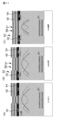
- the “light field intensity” is a light field intensity as a function of the distance L from the Z axis in the XY plane. Generally, in the basic mode, the light field intensity decreases monotonously as the distance L increases. Decreases as the distance L increases (see the conceptual diagram in FIG. 11A) while increasing or decreasing one or more times. In FIG. 11, the solid line represents the fundamental mode light field intensity distribution, and the broken line represents the higher-order mode light field intensity distribution.
- an object of the present disclosure is to provide a light emitting element having a configuration and a structure that can bring oscillation mode loss into a desired state.
- the light emitting device for achieving the above object is (A) a first compound semiconductor layer made of a GaN-based compound semiconductor and having a first surface and a second surface facing the first surface; An active layer made of a GaN-based compound semiconductor and in contact with the second surface of the first compound semiconductor layer; and A second compound semiconductor layer comprising a GaN-based compound semiconductor, having a first surface and a second surface facing the first surface, the first surface being in contact with the active layer; A laminated structure formed by laminating (B) a mode loss acting portion that is provided on the second surface of the second compound semiconductor layer and that constitutes a mode loss acting region that acts to increase or decrease the oscillation mode loss; (C) a second electrode formed over the mode loss acting part from the second surface of the second compound semiconductor layer; (D) a second light reflecting layer formed on the second electrode; (E) a first light reflecting layer formed on the first surface of the first compound semiconductor layer, and (F) a first electrode electrically connected to the first compound
- the light emitting device for achieving the above object is: (A) a first compound semiconductor layer made of a GaN-based compound semiconductor and having a first surface and a second surface facing the first surface; An active layer made of a GaN-based compound semiconductor and in contact with the second surface of the first compound semiconductor layer; and A second compound semiconductor layer comprising a GaN-based compound semiconductor, having a first surface and a second surface facing the first surface, the first surface being in contact with the active layer; A laminated structure formed by laminating (B) a second electrode formed on the second surface of the second compound semiconductor layer; (C) a second light reflecting layer formed on the second electrode; (D) a mode loss acting part that forms a mode loss acting region that is provided on the first surface of the first compound semiconductor layer and acts to increase or decrease the oscillation mode loss; (E) a first light reflecting layer formed over the mode loss acting part from the first surface of the first compound semiconductor layer, and (F) a first electrode electrically connected to the first compound semiconductor
- the stacked structure includes a current injection region, a current non-injection / inner region surrounding the current injection region, and a current non-injection / inner region.
- a current non-injection / outer region is formed, and the projection image of the mode loss action region and the projection image of the current non-injection / outer region overlap. That is, the current injection region and the mode loss action region are separated (separated) by the current non-injection / inner region. Therefore, by appropriately determining the positional relationship between the current injection region and the mode loss action region, the thickness of the mode loss action region constituting the mode loss action region, etc., it is possible to make the oscillation mode loss increase or decrease as desired. It becomes.
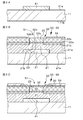
- FIG. 1 is a schematic partial cross-sectional view of the light emitting device of Example 1.
- FIG. 2A, 2B, and 2C are schematic partial cross-sectional views of a laminated structure and the like for explaining the method for manufacturing the light-emitting element of Example 1.
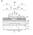
- FIG. 3 is a schematic partial cross-sectional view of the light-emitting element of Example 2.
- 4 is a schematic partial cross-sectional view of the light emitting device of Example 3.
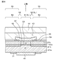
- FIG. 5 is a schematic partial cross-sectional view of the light emitting device of Example 4.
- 6 is a schematic partial cross-sectional view in which a main part of the light-emitting element of Example 4 shown in FIG. 5 is cut out.
- FIG. 1 is a schematic partial cross-sectional view of the light emitting device of Example 1.
- FIG. 2A, 2B, and 2C are schematic partial cross-sectional views of a laminated structure and the like for explaining the method for manufacturing the light-emitting element of Example 1.
- FIG. 3
- FIG. 7 is a schematic partial cross-sectional view of the light emitting device of Example 5.
- FIG. 8 is a schematic partial cross-sectional view of a modification of the light-emitting element of Example 5.
- FIG. 9 is a schematic partial cross-sectional view of another modification of the light-emitting element of Example 5.
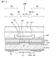
- FIG. 10 is a schematic partial cross-sectional view of the light-emitting element of Example 6.
- A), (B), and (C) of FIG. 11 are conceptual diagrams showing light field intensities in the conventional light emitting device, the light emitting device of Example 1, and the light emitting device of Example 4, respectively.
- Example 1 Light-emitting element according to the first aspect of the present disclosure
- Example 2 Modification of Example 1 4
- Example 3 Modification of Examples 1 and 2) 5
- Example 4 Modification of Examples 1 to 3) 6
- Example 5 Modification of Examples 1 to 4) 7
- Example 6 Light Emitting Element According to Second Embodiment of Present Disclosure
- a current non-injection region (a general term for a current non-injection / inner region and a current non-injection / outer region) is formed in the stacked structure.
- the current non-injection region may be formed in the thickness direction, a region on the second electrode side of the second compound semiconductor layer, or may be formed in the entire second compound semiconductor layer.
- it may be formed in the second compound semiconductor layer and the active layer, or may be formed from the second compound semiconductor layer to a part of the first compound semiconductor layer.
- the projected image of the mode loss effect region and the projected image of the current non-injection / outer region overlap, but in a region sufficiently away from the current injection region, the projection image of the mode loss effect region and the current non-injection / outer region are projected. It does not have to overlap with the image.
- the current non-injection / outer region may be located below the mode loss acting region.
- the current non-injection / inner region and the current non-injection / outer region are formed by ion implantation into the stacked structure. It can be configured.
- the light-emitting element having such a configuration is referred to as “a light-emitting element according to the first-A aspect of the present disclosure” and “a light-emitting element according to the second-A aspect of the present disclosure”.
- the ionic species may be at least one ion selected from the group consisting of boron, proton, phosphorus, arsenic, carbon, nitrogen, fluorine, oxygen, germanium, and silicon.
- the current non-injection / inner region and the current non-injection / outer region are the second of the second compound semiconductor layer.
- the surface may be formed by plasma irradiation, ashing treatment on the second surface of the second compound semiconductor layer, or reactive ion etching treatment on the second surface of the second compound semiconductor layer.
- the light-emitting element having such a configuration is referred to as “a light-emitting element according to the first-B aspect of the present disclosure” and “a light-emitting element according to the second-B aspect of the present disclosure”.
- the current non-injection / inner region and the current non-injection / outer region are exposed to plasma particles, so that the conductivity of the second compound semiconductor layer deteriorates, and the current non-injection / inner region and current The non-injection / outer region is in a high resistance state. That is, the current non-injection / inner region and the current non-injection / outer region can be formed by exposure of the second surface of the second compound semiconductor layer to the plasma particles.
- the plasma particles include argon, oxygen, nitrogen and the like.
- the second light reflecting layer may transmit light from the first light reflecting layer to the first light reflecting layer. It can be set as the structure which has an area
- the light-emitting element having such a configuration is referred to as “a light-emitting element according to the first-C aspect of the present disclosure” and “a light-emitting element according to the second-C aspect of the present disclosure”.
- the region of the second light reflecting layer located above the side wall of the mode loss acting part has a forward tapered slope, or alternatively 1 It has the area
- the first light reflecting layer transmits light from the second light reflecting layer to the first light reflecting layer. It can be set as the structure which has an area
- the light-emitting elements having such a configuration are referred to as “light-emitting elements according to the first-C ′ aspect of the present disclosure” and “light-emitting elements according to the second-C ′ aspect of the present disclosure”.
- a forward tapered slope is formed in a partial region of the first light reflection layer, or the second light A convex curved portion may be formed toward the reflective layer.
- the first light reflecting layer positioned above the side wall of the mode loss action part (the side wall of the opening provided in the mode loss action part).
- the region has a forward tapered inclination, or alternatively has a region curved convexly toward the second light reflecting layer.
- the first light reflecting layer and the second light reflecting layer It can also be set as the structure which scatters light toward the outer side of the resonator structure comprised.
- the second compound semiconductor is formed from the active layer in the current injection region.
- L 2 optical distance to the second surface of the layer
- L 0 optical distance from the active layer in the mode loss acting region to the top surface of the mode loss acting site
- the optical distance to the first surface of the compound semiconductor layer is L 1 ′ and the optical distance from the active layer in the mode loss action region to the top surface of the mode loss action site is L 0 ′, L 0 '> L 1 ' It can be set as the structure which satisfies these.
- the generated light having the higher-order mode is separated from the first light reflection layer and the first light reflection layer by the mode loss action region.
- a structure in which the oscillation mode loss is increased by being dissipated toward the outside of the resonator structure constituted by the two light reflection layers can be obtained. That is, the generated fundamental mode and higher-order mode light field intensities decrease with increasing distance from the Z axis in the projected image of the mode loss action region due to the presence of the mode loss action region that acts to increase or decrease the oscillation mode loss. Since there is more mode loss of higher order modes than the reduction of the light field intensity, the fundamental mode can be further stabilized, and mode loss can be suppressed compared to the case where there is no current injection inner region, The threshold current can be reduced.
- the mode loss action site may be configured of a dielectric material, a metal material, or an alloy material.
- the dielectric material include SiO x , SiN x , AlN x , AlO x , TaO x , and ZrO x
- the metal material or alloy material include titanium, gold, platinum, or alloys thereof. However, it is not limited to these materials.
- the mode loss acting part may be made of a dielectric material, and the optical thickness of the mode loss acting part may be configured to deviate from an integral multiple of 1/4 of the wavelength of light generated in the light emitting element.
- the standing wave can be destroyed by disturbing the phase of the light that circulates in the resonator and forms a standing wave at the mode loss acting portion, and a mode loss corresponding to that can be given.
- the mode loss acting part may be made of a dielectric material, and the optical thickness of the mode loss acting part may be an integral multiple of 1/4 of the wavelength of light generated in the light emitting element.
- the optical thickness of the mode loss acting part can be configured such that the phase of light generated in the light emitting element is not disturbed and the standing wave is not destroyed. However, it does not have to be exactly an integral multiple of 1/4. ( ⁇ / 4n 0 ) ⁇ m ⁇ ( ⁇ / 8n 0 ) ⁇ t 0 ⁇ ( ⁇ / 4n 0 ) ⁇ 2m + ( ⁇ / 8n 0 ) Should be satisfied.
- the mode loss acting part is made of a dielectric material, a metal material, or an alloy material, so that light passing through the mode loss acting part can be disturbed in phase or absorbed by the mode loss acting part.
- the oscillation mode loss can be controlled with a higher degree of freedom, and the design freedom of the light emitting element can be further increased.
- a convex portion is formed on the second surface side of the second compound semiconductor layer,
- the mode loss acting part can be configured to be formed on the region of the second surface of the second compound semiconductor layer surrounding the convex part.
- the light emitting element having such a configuration is referred to as “a light emitting element according to the first-D aspect of the present disclosure” for convenience.
- the convex portion occupies the current injection region and the current non-injection / inner region.
- the optical distance from the active layer in the current injection region to the second surface of the second compound semiconductor layer is L 2
- the optical distance from the active layer in the mode loss acting region to the top surface of the mode loss acting site is L 2.
- a convex portion is formed on the first surface side of the first compound semiconductor layer
- the mode loss acting part is formed on the region of the first surface of the first compound semiconductor layer surrounding the convex part, or the mode loss acting part is composed of the region of the first compound semiconductor layer surrounding the convex part. It can be set as a structure.
- the light emitting element having such a configuration is referred to as “a light emitting element according to the 2-D aspect of the present disclosure” for convenience.
- the convex portions coincide with the projected images of the current injection region and the current non-injection / inner region.
- the optical distance from the active layer in the current injection region to the first surface of the first compound semiconductor layer is L 1 ′
- the optical distance from the active layer in the mode loss action region to the top surface of the mode loss action site is When L 0 ' L 0 ' ⁇ L 1 '
- the mode loss acting site may be made of a dielectric material, a metal material, or an alloy material.
- examples of the dielectric material, the metal material, or the alloy material include the various materials described above.
- the second electrode can be made of a transparent conductive material.
- light-emitting elements of the present disclosure From the light-emitting elements according to the first to second aspects of the present disclosure including the preferable modes and configurations described above (hereinafter, these are collectively referred to simply as “light-emitting elements of the present disclosure”).
- a surface emitting laser element (vertical cavity laser, VCSEL) that emits laser light from the top surface of the one compound semiconductor layer through the first light reflecting layer can be configured, or alternatively, the second compound semiconductor layer
- a surface emitting laser element that emits laser light from the top surface through the second light reflecting layer can also be configured.
- the distance from the first light reflecting layer to the second light reflecting layer is preferably 0.15 ⁇ m or more and 50 ⁇ m or less, but is not limited thereto.
- At least the second light reflection layer may be fixed to the support substrate.
- the area centroid of the active layer may not exist on the normal line to the first light refracting layer passing through the area centroid of the first light reflecting layer.
- the first compound semiconductor layer is formed by lateral growth using a method of epitaxially growing in the lateral direction such as ELO (Epitaxial Lateral Overgrowth) method on the light emitting element manufacturing substrate on which the first light reflecting layer is formed.
- ELO Epitaxial Lateral Overgrowth
- the first compound semiconductor layer epitaxially grows from the edge of the first light reflecting layer toward the center of the first light reflecting layer many crystal defects may occur in the associated portion. If the association portion where many crystal defects are present is located at the center of the current injection region, the characteristics of the light emitting element may be adversely affected.
- the area centroid point of the active layer may not exist on the normal line to the first light reflection layer passing through the area centroid point of the first light reflection layer.
- the form in which the area center of gravity of the second light reflecting layer does not exist on the normal line to the first light reflecting layer passing through the area center of gravity of the first light reflecting layer, the first light reflecting layer passing through the area center of gravity of the first light reflecting layer By taking a form in which the area centroid of the active layer does not exist on the normal line to the above, the occurrence of adverse effects on the characteristics of the light emitting element can be reliably suppressed.
- the laminated structure can be specifically configured from an AlInGaN-based compound semiconductor.
- AlInGaN-based compound semiconductor examples include GaN, AlGaN, InGaN, and AlInGaN.
- these compound semiconductors may contain boron (B) atoms, thallium (Tl) atoms, arsenic (As) atoms, phosphorus (P) atoms, and antimony (Sb) atoms as desired.
- the active layer desirably has a quantum well structure. Specifically, it may have a single quantum well structure (SQW structure) or a multiple quantum well structure (MQW structure).
- An active layer having a quantum well structure has a structure in which at least one well layer and a barrier layer are stacked.
- a compound semiconductor constituting a well layer, a compound semiconductor constituting a barrier layer In y Ga (1-y) N, GaN), (In y Ga (1-y) N, In z Ga (1-z) N) [where y> z], (In y Ga (1-y ) N, AlGaN).
- the first compound semiconductor layer is composed of a compound semiconductor of a first conductivity type (for example, n-type)
- the second compound semiconductor layer is composed of a compound semiconductor of a second conductivity type (for example, p-type) different from the first conductivity type. Can be configured.
- the first compound semiconductor layer and the second compound semiconductor layer are also called a first cladding layer and a second cladding layer.
- the first compound semiconductor layer and the second compound semiconductor layer may be a layer having a single structure, a layer having a multilayer structure, or a layer having a superlattice structure. Furthermore, it can also be set as the layer provided with the composition gradient layer and the density
- the laminated structure is formed on the first surface of the light emitting element manufacturing substrate.
- a GaN substrate, sapphire substrate, GaAs substrate, SiC substrate, alumina substrate, ZnS substrate, ZnO substrate, AlN substrate are used as the light emitting element manufacturing substrate.
- Use is preferred because of low defect density.
- the characteristics of a GaN substrate vary depending on the growth surface, that is, polarity / nonpolarity / semipolarity, any main surface of the GaN substrate can be used for forming a compound semiconductor layer.
- a plane, B plane, C plane, R plane, M plane, N plane, S plane, etc. A crystal orientation plane called by name, or a plane in which these are turned off in a specific direction can also be used.
- Examples of methods for forming various compound semiconductor layers constituting light-emitting elements include metal organic chemical vapor deposition (MOCVD, Metal Organic-Chemical Vapor Deposition, MOVPE, Metal Organic-Vapor Phase Epitaxy) and molecules Line epitaxy method (MBE method), hydride vapor phase growth method (HVPE method) in which halogen contributes to transport or reaction, atomic layer deposition method (ALD method, Atomic Layer Deposition method), migration enhanced epitaxy method (MEE method, Migration-enhanced epitaxy method), plasma-assisted physical vapor deposition method (PPD method), and the like, but are not limited thereto.
- MOCVD Metal Organic-Chemical Vapor Deposition
- MOVPE Metal Organic-Vapor Phase Epitaxy
- MBE method molecules Line epitaxy method
- HVPE method hydride vapor phase growth method
- ALD method Atomic Layer Deposition method
- MEE method migration enhanced epitaxy method
- PPD method plasma-assisted physical vapor
- trimethylgallium (TMG) gas and triethylgallium (TEG) gas can be exemplified as the organic gallium source gas in the MOCVD method, and ammonia gas and hydrazine gas can be exemplified as the nitrogen source gas.
- silicon (Si) may be added as an n-type impurity (n-type dopant), or a GaN-based compound semiconductor having p-type conductivity.
- magnesium (Mg) may be added as a p-type impurity (p-type dopant).
- trimethylaluminum (TMA) gas may be used as the Al source, and trimethylindium (TMI) gas may be used as the In source. Good.
- monosilane gas (SiH 4 gas) may be used as the Si source, and biscyclopentadienyl magnesium gas, methylcyclopentadienyl magnesium, or biscyclopentadienyl magnesium (Cp 2 Mg) may be used as the Mg source.
- examples of n-type impurities (n-type dopants) include Ge, Se, Sn, C, Te, S, O, Pd, and Po.
- p-type impurities (p-type dopants) In addition to Mg, Zn, Cd, Be, Ca, Ba, C, Hg, and Sr can be mentioned.
- the support substrate may be composed of, for example, various substrates exemplified as a substrate for manufacturing a light emitting element, or may be an insulating substrate made of AlN or the like, a semiconductor substrate made of Si, SiC, Ge, or the like, a metal substrate, Although it can be composed of an alloy substrate, it is preferable to use a conductive substrate. Alternatively, from the viewpoint of mechanical properties, elastic deformation, plastic deformation, heat dissipation, etc., a metal substrate or an alloy substrate is used. It is preferable to use it. Examples of the thickness of the support substrate include 0.05 mm to 0.5 mm.
- a known method such as a solder bonding method, a room temperature bonding method, a bonding method using an adhesive tape, or a bonding method using wax bonding can be used. From the viewpoint of securing the property, it is desirable to employ a solder bonding method or a room temperature bonding method.
- a silicon semiconductor substrate which is a conductive substrate is used as a support substrate, it is desirable to employ a method capable of bonding at a low temperature of 400 ° C. or lower in order to suppress warping due to a difference in thermal expansion coefficient.
- the bonding temperature may be 400 ° C. or higher.
- the substrate for manufacturing the light emitting element may be left as it is, or the active layer, the second compound semiconductor layer, the second electrode, and the second light reflecting layer on the first compound semiconductor layer. If the first light reflecting layer is formed after the sequential formation, the light emitting element manufacturing substrate may be removed using the first light reflecting layer as a stopper layer. Specifically, an active layer, a second compound semiconductor layer, a second electrode, and a second light reflection layer are sequentially formed on the first compound semiconductor layer, and then the second light reflection layer is fixed to the support substrate.
- the light emitting element manufacturing substrate is removed using the first light reflecting layer as a stopper layer, and the first compound semiconductor layer (the first surface of the first compound semiconductor layer) and the first light reflecting layer are removed.
- One light reflecting layer may be exposed.
- the first electrode may be formed on the first compound semiconductor layer (the first surface of the first compound semiconductor layer).
- the removal of the light emitting element manufacturing substrate can be performed based on a chemical / mechanical polishing method (CMP method).
- CMP method chemical / mechanical polishing method
- alkaline aqueous solution such as sodium hydroxide aqueous solution or potassium hydroxide aqueous solution, ammonia solution + hydrogen peroxide solution, sulfuric acid solution + hydrogen peroxide solution, hydrochloric acid solution + hydrogen peroxide solution, phosphoric acid solution + hydrogen peroxide solution
- a part of the substrate for manufacturing a light emitting device is removed by a wet etching method using a dry etching method, a dry etching method, a lift-off method using a laser, a mechanical polishing method, or a combination thereof, or a light emitting device
- the first compound semiconductor layer the first surface of the first compound semiconductor layer
- the first light reflecting layer may be exposed.
- the GaN substrate is known to change its polarity / polarity / semipolarity depending on the growth surface, but any main surface of the GaN substrate can be used for forming the compound semiconductor layer. Further, regarding the main surface of the GaN substrate, depending on the crystal structure (for example, cubic type, hexagonal type, etc.), names such as so-called A plane, B plane, C plane, R plane, M plane, N plane, S plane, etc. A plane (including the case where the off angle is 0 degree) in which the plane orientation of the crystal plane is called off in a specific direction is used.
- the first electrode may be formed on the second surface facing the first surface of the light emitting element manufacturing substrate when the light emitting element manufacturing substrate remains. Moreover, what is necessary is just to form on the 1st surface of the 1st compound semiconductor layer which comprises a laminated structure, when the board
- the first electrode is, for example, gold (Au), silver (Ag), palladium (Pd), platinum (Pt), nickel (Ni), Ti (titanium), vanadium (V), tungsten (W), chromium (Cr ), Al (aluminum), Cu (copper), Zn (zinc), tin (Sn) and at least one metal selected from the group consisting of indium (In) (including alloys) or It is desirable to have a multilayer structure, specifically, for example, Ti / Au, Ti / Al, Ti / Al / Au, Ti / Pt / Au, Ni / Au, Ni / Au / Pt, Ni / Pt, Pd / Pt and Ag / Pd can be exemplified.
- the first electrode can be formed by, for example, a PVD method such as a vacuum evaporation method or a sputtering method.
- the first electrode When the first electrode is formed so as to surround the first light reflection layer, the first light reflection layer and the first electrode may be in contact with each other. Alternatively, the first light reflection layer and the first electrode may be separated from each other, that is, have an offset, and the separation distance may be within 1 mm.
- the separation distance When the current injection region located in the first light reflecting layer and the first electrode are separated from each other in plan, the current flows through the first compound semiconductor layer for a long distance. Therefore, in order to keep the electric resistance generated in this current path low, the separation distance is preferably within 1 mm. In some cases, the state where the first electrode is formed up to the edge of the first light reflecting layer, and the state where the first light reflecting layer is formed up to the edge of the first electrode are mentioned. You can also.
- the first electrode when the first light reflecting layer is formed even on the edge of the first electrode, the first electrode has a certain degree so as not to absorb the fundamental mode light of laser oscillation as much as possible. It is necessary to have an opening having a size of. The size of the opening varies depending on the wavelength of the fundamental mode and the optical confinement structure in the lateral direction (the in-plane direction of the first compound semiconductor layer), but is not limited, but is approximately several times the oscillation wavelength ⁇ . It is preferable that
- indium-tin composite oxide including ITO, Indium Tin Oxide, Sn-doped In 2 O 3 , crystalline ITO and amorphous ITO
- ITiO Ti-doped In 2 O 3
- Indium-Zinc Oxide IZO
- IFO F-doped In 2 O 3
- tin oxide SnO 2
- ATO Sb-doped SnO 2
- FTO F-doped SnO 2
- zinc oxide including ZnO, Al-doped ZnO and B-doped ZnO
- indium-doped gallium-zinc composite oxide IGZO, In—GaZnO 4
- aluminum oxide-doped zinc oxide AZO
- AlMgZnO aluminum oxide and magnesium oxide-doped zinc oxide
- IGO InS ZnO, NiO, or can be exempl
- a transparent conductive film having a base layer of gallium oxide, titanium oxide, niobium oxide, nickel oxide, or the like can be given.
- the second electrode may be composed of at least one of these materials.
- the second electrode can be formed by, for example, a PVD method such as a vacuum evaporation method or a sputtering method.
- a pad electrode may be provided on the first electrode or the second electrode for electrical connection with an external electrode or circuit.
- the pad electrode includes a single layer containing at least one metal selected from the group consisting of Ti (titanium), aluminum (Al), Pt (platinum), Au (gold), Ni (nickel), and Pd (palladium). It is desirable to have a configuration or a multi-layer configuration.
- the pad electrode may be a Ti / Pt / Au multilayer structure, a Ti / Au multilayer structure, a Ti / Pd / Au multilayer structure, a Ti / Pd / Au multilayer structure, a Ti / Ni / Au multilayer structure, A multi-layer structure exemplified by a multi-layer structure of Ti / Ni / Au / Cr / Au can also be used.
- the first electrode is composed of an Ag layer or an Ag / Pd layer
- a cover metal layer made of Ni / TiW / Pd / TiW / Ni is formed on the surface of the first electrode, and on the cover metal layer,
- the light reflecting layer (distributed Bragg reflector layer, distributed Bragg reflector layer, DBR layer) constituting the first light reflecting layer and the second light reflecting layer is composed of, for example, a semiconductor multilayer film or a dielectric multilayer film.
- the dielectric material include oxides and nitrides such as Si, Mg, Al, Hf, Nb, Zr, Sc, Ta, Ga, Zn, Y, B, and Ti (for example, SiN x , AlN x , and AlGaN).
- X , GaN X , BN X, etc. or fluorides.
- a light reflection layer can be obtained by laminating
- a multilayer film such as SiO x / SiN y , SiO x / NbO y , SiO x / ZrO y , SiO x / AlN y is preferable.
- each dielectric film may be appropriately selected.
- the thickness of each dielectric film can be appropriately adjusted depending on the material used and the like, and is determined by the oscillation wavelength (emission wavelength) ⁇ and the refractive index n at the oscillation wavelength ⁇ of the material used. Specifically, an odd multiple of ⁇ / (4n) is preferable.
- ⁇ emission wavelength
- n refractive index
- the light reflecting layer can be formed based on a well-known method. Specifically, for example, a vacuum deposition method, a sputtering method, a reactive sputtering method, an ECR plasma sputtering method, a magnetron sputtering method, an ion beam assisted deposition method, PVD methods such as ion plating method and laser ablation method; various CVD methods; coating methods such as spray method, spin coating method, dip method; method combining two or more of these methods; these methods and all or part A combination of at least one of typical pretreatment, inert gas (Ar, He, Xe, etc.) or plasma irradiation, oxygen gas or ozone gas, plasma irradiation, oxidation treatment (heat treatment), exposure treatment, etc. Can be mentioned.
- the first light reflecting layer preferably includes a dielectric film containing at least N (nitrogen) atoms. Furthermore, the dielectric film containing N atoms is the outermost layer of the dielectric multilayer film. The upper layer is more desirable.
- the first light reflecting layer is preferably covered with a dielectric material layer containing at least N (nitrogen) atoms. Alternatively, by nitriding the surface of the first light reflecting layer, the surface of the first light reflecting layer is referred to as a layer containing at least N (nitrogen) atoms (hereinafter referred to as “surface layer” for convenience). ) Is desirable.
- the thickness of the dielectric film or dielectric material layer containing at least N atoms, or the surface layer is preferably an odd multiple of ⁇ / (4n).
- the material constituting at least containing a N atom dielectric film or a dielectric material layer specifically, mention may be made of SiN X, the SiO Y N Z.
- the size and shape of the light reflecting layer are not particularly limited as long as it covers the current injection region.
- the shape of the boundary between the current injection region and the current non-injection / inner region, and the shape of the boundary between the current non-injection / inner region and the current non-injection / outer region are specifically circular, elliptical, rectangular, and polygonal. (Triangle, square, hexagon, etc.). It is desirable that the shape of the boundary between the current injection region and the current non-injection / inner region and the shape of the boundary between the current non-injection / inner region and the current non-injection / outer region are similar.
- the diameter is preferably about 5 ⁇ m to 100 ⁇ m.
- the side surface and the exposed surface of the laminated structure may be covered with an insulating film.
- the insulating film can be formed based on a known method.
- the refractive index of the material constituting the insulating film is preferably smaller than the refractive index of the material constituting the laminated structure.
- SiO X based material containing SiO 2, SiN X-based material, SiO Y N Z material, TaO X, ZrO X, AlN X, AlO X can be exemplified a GaO X
- organic materials such as polyimide resin can also be mentioned.
- a PVD method such as a vacuum vapor deposition method or a sputtering method, or a CVD method can be given, and it can also be formed based on a coating method.
- Example 1 relates to a light-emitting element according to the first aspect of the present disclosure, specifically, a light-emitting element according to the first-A aspect of the present disclosure. More specifically, the light-emitting elements of Example 1 or Examples 2 to 4 to be described later are surface emitting in which laser light is emitted from the top surface of the second compound semiconductor layer 22 through the second light reflecting layer 42. It consists of a laser element (vertical cavity laser, VCSEL).
- VCSEL vertical cavity laser
- a schematic partial end view of the light emitting device of Example 1 shown in FIG. 1 or the light emitting devices of Examples 2 to 5 to be described later is as follows.
- A a first compound semiconductor layer 21 made of a GaN-based compound semiconductor and having a first surface 21a and a second surface 21b facing the first surface 21a;
- An active layer (light emitting layer) 23 made of a GaN-based compound semiconductor and in contact with the second surface 21b of the first compound semiconductor layer 21, and
- a second compound semiconductor layer 22 made of a GaN-based compound semiconductor, having a first surface 22a and a second surface 22b opposite to the first surface 22a, the first surface 22a being in contact with the active layer 23;
- a laminated structure 20 formed by laminating (B) a mode loss acting part (mode loss acting layer) 54 that is provided on the second surface 22b of the second compound semiconductor layer 22 and constitutes a mode loss acting region 55 that acts to increase or decrease the oscillation mode loss;
- C a second electrode 32 formed over the mode loss acting
- the laminated structure 20 is formed on the first surface 11a of the light-emitting element manufacturing substrate 11 having conductivity.
- the first electrode 31 is formed on the second surface 11 b facing the first surface 11 a of the light emitting element manufacturing substrate 11.
- the stacked structure 20 includes a current injection region 51, a current non-injection / inner region 52 surrounding the current injection region 51, and a current non-injection / outer region 53 surrounding the current non-injection / inner region 52. Therefore, the projection image of the mode loss action region 55 and the projection image of the current non-injection / outer region 53 overlap each other. That is, the current non-injection / outer region 53 is located below the mode loss action region 55. In a region sufficiently separated from the current injection region 51 where current is injected, the projection image of the mode loss action region 55 and the projection image of the current non-injection / outer region 53 may not overlap.
- current non-injection regions 52 and 53 into which no current is injected are formed.
- the current non-injection regions 52 and 53 may be formed in the thickness direction, in the region on the second electrode side of the second compound semiconductor layer 22, or may be formed in the entire second compound semiconductor layer 22. Alternatively, it may be formed in the second compound semiconductor layer 22 and the active layer 23.
- the mode loss acting part (mode loss acting layer) 54 is made of a dielectric material such as SiO 2, and in the light emitting device of Example 1 or Examples 2 to 5 described later, the second electrode 32 and the second compound semiconductor layer 22 are used. Is formed between.
- the optical thickness of the mode loss acting part 54 can be set to a value deviating from an integral multiple of 1/4 of the wavelength of light generated in the light emitting element.
- the optical thickness of the mode loss acting portion 54 can be an integral multiple of 1/4 of the wavelength of light generated in the light emitting element. That is, the optical thickness of the mode loss acting part 54 can be set to a thickness that does not disturb the phase of the light generated in the light emitting element and does not destroy the standing wave.
- the optical thickness of the mode loss acting portion 54 is preferably about 25 to 250 when a value of 1 ⁇ 4 of the wavelength of light generated in the light emitting element is “100”.
- the optical distance from the active layer 23 to the second surface of the second compound semiconductor layer 22 in the current injection region 51 is L 2
- L 0 the optical distance from the active layer 23 in the mode loss acting region 55 to the top surface of the mode loss acting region 54 (the surface facing the second electrode 32)
- L 0 / L 2 1.5 It was.
- the generated laser light having a higher-order mode is dissipated toward the outside of the resonator structure constituted by the first light reflection layer 41 and the second light reflection layer 42 by the mode loss action region 55, and As a result, the oscillation mode loss increases.
- the generated fundamental mode and higher-order mode light field intensities decrease with increasing distance from the Z axis in the projected image of the mode loss action region 55 due to the presence of the mode loss action region 55 that acts to increase or decrease the oscillation mode loss.
- the decrease in the light field intensity in the higher order mode is more than the decrease in the light field intensity in the fundamental mode
- the fundamental mode can be further stabilized, and the threshold The current can be reduced, and the relative light field intensity of the fundamental mode can be increased.
- the skirt portion of the high-order mode light field intensity is located farther from the current injection region than the conventional light emitting element (see FIG. 11A), the influence of the reverse lens effect can be reduced. Can be planned. In the first place, when the mode loss action part 54 made of SiO 2 is not provided, a mixture of oscillation modes occurs.
- the first compound semiconductor layer 21 is composed of an n-GaN layer, and the active layer 23 is a five-fold multiple quantum well in which an In 0.04 Ga 0.96 N layer (barrier layer) and an In 0.16 Ga 0.84 N layer (well layer) are stacked.
- the second compound semiconductor layer 22 is composed of a p-GaN layer.
- the first electrode 31 is made of Ti / Pt / Au, and the second electrode 32 is made of a transparent conductive material, specifically, ITO.
- a circular opening 54A is formed in the mode loss acting portion 54, and the second compound semiconductor layer 22 is exposed at the bottom of the opening 54A.
- a pad electrode (not shown) made of, for example, Ti / Pt / Au or V / Pt / Au for electrically connecting to an external electrode or circuit is formed on the edge of the first electrode 31 or It is connected.
- a pad electrode 33 made of, for example, Ti / Pd / Au or Ti / Ni / Au is formed or connected to be electrically connected to an external electrode or circuit.
- the first light reflection layer 41 and the second light reflection layer 42 have a stacked structure of SiN layers and SiO 2 layers (total number of stacked dielectric films: 20 layers).
- the first light reflection layer 41 and the second light reflection layer 42 have a multilayer structure as described above, but are represented by one layer for the sake of simplification of the drawing.
- the distance from the first light reflection layer 41 to the second light reflection layer 42 is not less than 0.15 ⁇ m and not more than 50 ⁇ m, and specifically, for example, 4.5 ⁇ m.
- the current non-injection / inner region 52 and the current non-injection / outer region 53 are formed by ion implantation into the stacked structure 20.
- boron is selected as the ion species, but it is not limited to boron ions.
- FIGS. 2A, 2B, and 2C are schematic partial end views of the laminated structure and the like.
- the first light reflecting layer 41 made of a multilayer film and having a convex shape is formed on the light emitting element manufacturing substrate 11. Specifically, on the first surface 11a of the light emitting element manufacturing substrate 11 made of a GaN substrate, a patterned first light reflecting layer 41 made of a multilayer film is formed based on a known method. In this way, the structure shown in FIG. 2A can be obtained.
- the shape of the first light reflecting layer 41 is a disc shape. However, the shape of the first light reflecting layer 41 is not limited to this.
- a first compound semiconductor layer 21 made of a GaN-based compound semiconductor and having a first surface 21a and a second surface 21b facing the first surface 21a;
- An active layer (light emitting layer) 23 made of a GaN-based compound semiconductor and in contact with the second surface 21b of the first compound semiconductor layer 21, and
- a second compound semiconductor layer 22 made of a GaN-based compound semiconductor, having a first surface 22a and a second surface 22b opposite to the first surface 22a, the first surface 22a being in contact with the active layer 23;
- a laminated structure 20 is formed by laminating layers.
- the first compound semiconductor layer 21 made of n-GaN is formed by lateral growth using a method of epitaxial growth in the lateral direction such as the ELO method, and further, on the basis of the epitaxial growth method,
- the stacked structure 20 can be obtained by forming the active layer 23 and the second compound semiconductor layer 22.
- Step-120 Thereafter, the current non-implanted / inner region 52 and the current non-implanted / outer region 53 are formed in the stacked structure 20 based on an ion implantation method using boron ions.
- a mode loss acting part (mode loss acting layer) 54 having an opening 54A and made of SiO 2 is formed based on a known method (see FIG. 2B). .
- the second electrode 32 is formed on the mode loss acting part (mode loss acting layer) 54 from the second surface 22b of the second compound semiconductor layer 22 exposed on the bottom surface of the opening 54A, for example, based on the lift-off method, Further, the pad electrode 33 is formed based on a known method. In this way, the structure shown in FIG. 2C can be obtained. Next, the second light reflecting layer 42 is formed on the pad electrode 33 from the second electrode 32 based on a known method. Thus, the structure shown in FIG. 1 can be obtained.
- the first electrode 31 and the like are formed on the second surface 11b of the light emitting element manufacturing substrate 11 based on a well-known method, and further, the light emitting element is separated by performing so-called element separation, and the side surface of the laminated structure or The exposed surface is covered with an insulating film made of, for example, SiO 2 . And the light emitting element of Example 1 is completed by packaging and sealing.
- the stacked structure includes a current injection region, a current non-injection / inner region surrounding the current injection region, and a current non-injection / outer region surrounding the current non-injection / inner region. Therefore, the projected image of the mode loss action region and the projected image of the current non-injection / outer region overlap. Therefore, as shown in the conceptual diagram of FIG. 11B, it is possible to increase or decrease the oscillation mode loss (specifically, increase in the first embodiment). As a result, for example, it is possible to solve the problems in the conventional light emitting device such that the threshold current increases or the slope efficiency deteriorates. For example, the threshold current can be reduced by reducing the oscillation mode loss in the fundamental mode.
- the degree of freedom of control and the degree of freedom of design of the light emitting element can be increased.
- the relationship between the magnitude of the oscillation mode loss that the mode loss action region gives to the fundamental mode and higher-order modes by setting the current injection region, the current non-injection region, and the mode loss action region as described above.
- the fundamental mode can be further stabilized by making the oscillation mode loss given to the higher-order mode relatively larger than the oscillation mode loss given to the fundamental mode.
- Example 2 is a modification of Example 1 and relates to a light-emitting element according to the first-B aspect of the present disclosure.
- the current non-injection / inner region 52 and the current non-injection / outer region 53 are formed on the second surface of the second compound semiconductor layer 22.
- RIE reactive ion etching
- the conductivity of the second compound semiconductor layer 22 is determined.
- the current non-injection / inner region 52 and the current non-injection / outer region 53 are in a high resistance state. That is, the current non-injection / inner region 52 and the current non-injection / outer region 53 are formed by exposure of the second surface 22b of the second compound semiconductor layer 22 to plasma particles.
- Example 2 instead of [Step-120] of Example 1, plasma irradiation to the second surface of the second compound semiconductor layer 22 or irradiation of the second surface of the second compound semiconductor layer 22 to the second surface is performed. Based on the ashing process or the reactive ion etching process on the second surface of the second compound semiconductor layer 22, the current non-injection / inner region 52 and the current non-injection / outer region 53 may be formed in the stacked structure 20. .
- Example 2 the configuration and structure of the light-emitting element of Example 2 can be the same as the structure and structure of the light-emitting element of Example 1, and thus detailed description thereof is omitted.
- the current injection region, the current non-injection region, and the mode loss action region have the predetermined arrangement relationship described above, so that the basic mode and the higher order mode can be obtained.
- Example 3 is a modification of Example 1 to Example 2, and relates to a light-emitting element according to the 1-C aspect of the present disclosure.
- the second light reflecting layer 42 transmits light from the first light reflecting layer 41 to the first light reflecting layer 41 and the first light reflecting layer 41. It has a region that reflects or scatters toward the outside of the resonator structure constituted by the two-light reflecting layer 42 (that is, toward the mode loss action region 55).
- the portion of the second light reflecting layer 42 located above the side wall (side wall of the opening 54B) of the mode loss acting part (mode loss acting layer) 54 has a forward tapered inclined portion 42A, or Further, it has a region curved convexly toward the first light reflecting layer 41.
- Example 3 the shape of the boundary between the current injection region 51 and the current non-injection / inner region 52 is circular (diameter: 8 ⁇ m), and the boundary between the current non-injection / inner region 52 and the current non-injection / outer region 53 is The shape was circular (diameter: 10 ⁇ m to 20 ⁇ m).
- Example 3 in the same process as [Step-130] of Example 1, when forming the mode loss action part (mode loss action layer) 54 having the opening 54B and made of SiO 2 , the forward taper is formed.
- An opening 54B having a side wall may be formed. Specifically, a resist layer is formed on the mode loss working layer formed on the second surface 22b of the second compound semiconductor layer 22, and the photolithography technique is applied to the portion of the resist layer where the opening 54B is to be formed. An opening is provided based on this. Based on a well-known method, the side wall of this opening is made into a forward taper shape. Then, by performing etch-back, an opening 54B having a forward tapered side wall can be formed in the mode loss action portion (mode loss action layer) 54. Furthermore, the second electrode 32 and the second light reflecting layer 42 are formed on such a mode loss acting part (mode loss acting layer) 54, so that a forward tapered inclined portion 42 ⁇ / b> A is formed on the second light reflecting layer 42. Can be granted
- Example 3 can be the same as the structure and structure of the light-emitting element of Example 1 to Example 2, and thus detailed description thereof is omitted.
- Example 4 is a modification of Example 1 to Example 3, and relates to a light-emitting element according to the 1st-D aspect of the present disclosure.
- a schematic partial cross-sectional view of the light-emitting element of Example 4 is shown in FIG. 5, and a schematic partial cross-sectional view with the main part cut out is shown in FIG. 6.
- a convex portion 22A is formed on the 22b side.
- the mode loss acting part (mode loss acting layer) 54 is formed on the region 22B of the second surface 22b of the second compound semiconductor layer 22 surrounding the convex portion 22A.
- the convex portion 22A occupies the current injection region 51, the current injection region 51, and the current non-injection / inner region 52.
- the mode loss acting part (mode loss acting layer) 54 is made of a dielectric material such as SiO 2 as in the first embodiment.
- a current non-injection / outer region 53 is provided in the region 22B.
- the generated laser light having a higher-order mode is confined in the current injection region 51 and the current non-injection / inner region 52 by the mode loss action region 55, so that the oscillation mode loss is reduced. Decrease. That is, the generated fundamental mode and higher-order mode light field intensities increase in the projected images of the current injection region 51 and the current non-injection / inner region 52 due to the presence of the mode loss action region 55 that acts to increase or decrease the oscillation mode loss.
- Example 4 the shape of the boundary between the current injection region 51 and the current non-injection / inner region 52 is circular (diameter: 8 ⁇ m), and the boundary between the current non-injection / inner region 52 and the current non-injection / outer region 53 is The shape was a circle (diameter: 30 ⁇ m).
- Example 4 a part of the second compound semiconductor layer 22 is removed from the second surface 22b side between [Step-120] and [Step-130] of Example 1 to obtain a convex shape. What is necessary is just to form the part 22A.
- the configuration and structure of the light-emitting element of Example 4 can be the same as the configuration and structure of the light-emitting element of Example 1, and thus detailed description thereof is omitted.
- the light emitting device of Example 4 it is possible to suppress the oscillation mode loss caused by the mode loss action region with respect to various modes, to not only cause the transverse mode to oscillate in multiple modes, but also to reduce the laser oscillation threshold.
- the optical field intensity of the generated fundamental mode and higher-order mode is increased or decreased (specifically, decreased in the fourth embodiment). Due to the presence of the acting mode loss action region, it can be increased in the projection image of the current injection region and the current non-injection / inner region.
- Example 5 is a modification of Example 1 to Example 4. More specifically, the light emitting element of Example 5 or Example 6 described later is a surface emitting laser element (vertical) that emits laser light from the top surface of the first compound semiconductor layer 21 via the first light reflecting layer 41. (Cavity laser, VCSEL).
- the second light reflecting layer 42 is made of a gold (Au) layer or a solder layer containing tin (Sn).
- the bonding layer 43 is fixed to a support substrate 44 made of a silicon semiconductor substrate based on a solder bonding method.
- Example 5 a method for manufacturing the light-emitting element of Example 5 will be described.
- Step-500 First, for example, by performing the same steps as [Step-100] to [Step-140] of Example 1, the state shown in FIG. 1 can be obtained. Alternatively, various manufacturing steps of the light emitting element described in the second to fourth embodiments are performed.
- Step-510 Thereafter, the second light reflecting layer 42 is fixed to the support substrate 44 through the bonding layer 43.
- the light emitting element manufacturing substrate 11 is removed to expose the first surface 21 a of the first compound semiconductor layer 21 and the first light reflecting layer 41. Specifically, first, the thickness of the light emitting element manufacturing substrate 11 is reduced based on the mechanical polishing method, and then the remaining part of the light emitting element manufacturing substrate 11 is removed based on the CMP method. Thus, the first surface 21a of the first compound semiconductor layer 21 and the first light reflecting layer 41 are exposed.
- Step-530 Thereafter, the first electrode 31 is formed on the first surface 21 a of the first compound semiconductor layer 21.
- the light emitting device of Example 5 having the structure shown in FIG. 7 can be obtained.
- the mode loss operation region is different from the basic mode and higher order modes by setting the current injection region, the current non-injection region, and the mode loss operation region to the predetermined arrangement relationship described above.
- the magnitude relationship of the oscillation mode loss to be applied can be controlled, and the fundamental mode can be further stabilized by making the oscillation mode loss to be given to the higher-order mode relatively larger than the oscillation mode loss to be given to the fundamental mode.
- the light emitting element manufacturing substrate is removed in a state where the first light reflection layer is formed. Therefore, as a result of the first light reflecting layer functioning as a kind of stopper when removing the light emitting element manufacturing substrate, the variation in removal of the light emitting element manufacturing substrate within the surface of the light emitting element manufacturing substrate, and further, the first compound semiconductor Generation of variations in layer thickness can be suppressed, and the length of the resonator can be made uniform. As a result, stabilization of characteristics of the obtained light emitting element can be achieved.
- the surface (flat surface) of the first compound semiconductor layer at the interface between the first light reflecting layer and the first compound semiconductor layer is flat, it is possible to minimize the scattering of laser light on the flat surface. it can.
- the end portion of the first electrode 31 is separated from the first light reflecting layer 41. That is, the first light reflection layer 41 and the first electrode 31 are separated from each other, in other words, have an offset, and the separation distance is within 1 mm, specifically, for example, an average of 0.05 mm. .
- the structure is not limited to such a structure, and the end of the first electrode 31 may be in contact with the first light reflecting layer 41, or the end of the first electrode 31 may be in contact with the first light reflecting layer 41. It may be formed on the edge.
- [Step-100] of Example 1 is omitted, and first, for example, after performing the same steps as [Step-110] to [Step-140] of Example 1, [Step-510] [Step-520] is performed to expose the first surface 21a of the first compound semiconductor layer 21, and then the first light reflecting layer 41 and the first electrode are formed on the first surface 21a of the first compound semiconductor layer 21. 31 may be formed.
- a schematic partial cross-sectional view of the light-emitting element thus obtained is shown in FIG. Further, when the first light reflecting layer 41 is formed on the first surface 21 a of the first compound semiconductor layer 21, the first compound semiconductor layer 21 is etched to form a recess in the first surface 21 a of the first compound semiconductor layer 21.
- the first light reflection layer 41 may be formed in the recess.
- the light emitting element according to the first-C ′ mode of the present disclosure can be obtained by making the side wall of the recess into a forward tapered shape (see FIG. 9). That is, the first light reflection layer 41 reflects or scatters light from the second light reflection layer 42 toward the outside of the resonator structure constituted by the first light reflection layer 41 and the second light reflection layer 42. Region (inclined portion 41A) to be used.
- Example 6 relates to a light-emitting element according to the second aspect of the present disclosure, specifically, a light-emitting element according to the second-A aspect of the present disclosure. More specifically, the light emitting device of Example 6 is a surface emitting laser device (vertical cavity laser, VCSEL) that emits laser light from the top surface of the first compound semiconductor layer 21 via the first light reflecting layer 41. Consists of.
- VCSEL vertical cavity laser
- the light emitting device of Example 6 whose schematic partial end view is shown in FIG. (A) a first compound semiconductor layer 21 made of a GaN-based compound semiconductor and having a first surface 21a and a second surface 21b facing the first surface 21a; An active layer (light emitting layer) 23 made of a GaN-based compound semiconductor and in contact with the second surface 21b of the first compound semiconductor layer 21, and A second compound semiconductor layer 22 made of a GaN-based compound semiconductor, having a first surface 22a and a second surface 22b opposite to the first surface 22a, the first surface 22a being in contact with the active layer 23; A laminated structure 20 formed by laminating (B) a second electrode 32 formed on the second surface 22b of the second compound semiconductor layer 22, (C) a second light reflecting layer 42 formed on the second electrode 32; (D) a mode loss acting portion 64 that is provided on the first surface 21a of the first compound semiconductor layer 21 and constitutes a mode loss acting region 65 that acts to increase or decrease the oscillation mode loss; (E) the first light
- the stacked structure 20 includes a current injection region 61, a current non-injection / inner region 62 surrounding the current injection region 61, and a current non-injection / outer region 63 surrounding the current non-injection / inner region 62. Therefore, the projection image of the mode loss action region 65 and the projection image of the current non-injection / outer region 63 overlap each other.
- the current non-injection regions 62 and 63 are formed in the stacked structure 20, in the illustrated example, the thickness direction extends from the second compound semiconductor layer 22 to a part of the first compound semiconductor layer 21. Is formed.
- the current non-injection regions 62 and 63 may be formed in the thickness direction, in the region on the second electrode side of the second compound semiconductor layer 22, or may be formed in the entire second compound semiconductor layer 22. Alternatively, it may be formed in the second compound semiconductor layer 22 and the active layer 23.
- the configuration of the laminated structure 20, the pad electrode 33, the first light reflection layer 41, and the second light reflection layer 42 can be the same as that of the first embodiment, and the configuration of the bonding layer 43 and the support substrate 44 can be implemented. Similar to Example 5, A circular opening 64A is formed in the mode loss acting portion 64, and the first surface 21a of the first compound semiconductor layer 21 is exposed at the bottom of the opening 64A.
- the mode loss acting part (mode loss acting layer) 64 is made of a dielectric material such as SiO 2 and is formed on the first surface 21 a of the first compound semiconductor layer 21.
- the optical thickness of the mode loss acting part 64 can be set to a value deviating from an integral multiple of 1/4 of the wavelength of light generated in the light emitting element.
- the optical thickness of the mode loss acting portion 64 can be an integral multiple of 1/4 of the wavelength of light generated in the light emitting element. That is, the optical thickness of the mode loss acting part 64 can be set to a thickness that does not disturb the phase of the light generated in the light emitting element and does not destroy the standing wave. However, it does not have to be exactly an integral multiple of 1/4.
- the optical thickness of the mode loss acting portion 64 is preferably about 25 to 250 when a value of 1 ⁇ 4 of the wavelength of light generated in the light emitting element is “100”. And by adopting these configurations, it is possible to change the phase difference between the laser light that passes through the mode loss acting portion 64 and the laser light that passes through the current injection region 61 (control the phase difference), The oscillation mode loss can be controlled with a higher degree of freedom, and the design freedom of the light emitting element can be further increased.
- the optical distance from the active layer 23 to the first surface of the first compound semiconductor layer 21 in the current injection region 61 is L 1 ′, and the active layer 23 to the mode loss action site 64 in the mode loss action region 65.
- L 0 ′ the optical distance to the top surface (surface facing the first electrode 31)
- L 0 '/ L 1 ' 1.01 It was.
- the generated laser light having a higher-order mode is dissipated toward the outside of the resonator structure constituted by the first light reflection layer 41 and the second light reflection layer 42 by the mode loss action region 65, and As a result, the oscillation mode loss increases.
- the generated fundamental mode and higher-order mode light field intensities decrease as the distance from the Z axis increases in the projected image of the mode loss action region 65 due to the presence of the mode loss action region 65 that acts to increase or decrease the oscillation mode loss.
- the decrease in the light field intensity in the higher order mode is more than the decrease in the light field intensity in the fundamental mode
- the fundamental mode can be further stabilized, and the threshold The current can be reduced, and the relative light field intensity of the fundamental mode can be increased.
- the current non-injection / inner region 62 and the current non-injection / outer region 63 are formed by ion implantation into the stacked structure 20 as in Example 1.
- boron is selected as the ion species, but it is not limited to boron ions.
- Example 6 a method for manufacturing the light-emitting element of Example 6 will be described.
- Step-600 First, on the light emitting element manufacturing substrate 11, A first compound semiconductor layer 21 made of a GaN-based compound semiconductor and having a first surface 21a and a second surface 21b facing the first surface 21a; An active layer (light emitting layer) 23 made of a GaN-based compound semiconductor and in contact with the second surface 21b of the first compound semiconductor layer 21, and A second compound semiconductor layer 22 made of a GaN-based compound semiconductor, having a first surface 22a and a second surface 22b opposite to the first surface 22a, the first surface 22a being in contact with the active layer 23; A laminated structure 20 is formed by laminating layers.
- the first compound semiconductor layer 21 made of n-GaN is formed by lateral growth using a method of epitaxial growth in the lateral direction such as the ELO method, and further, on the basis of the epitaxial growth method,
- the stacked structure 20 can be obtained by forming the active layer 23 and the second compound semiconductor layer 22.
- Step-610 Thereafter, a current non-implanted / inner region 62 and a current non-implanted / outer region 63 are formed in the stacked structure 20 based on an ion implantation method using boron ions.
- the second electrode 32 is formed on the second surface 22b of the second compound semiconductor layer 22 based on, for example, a lift-off method, and further the pad electrode 33 is formed based on a known method. Thereafter, the second light reflection layer 42 is formed on the pad electrode 33 from the second electrode 32 based on a known method.
- Step-630 Thereafter, the second light reflecting layer 42 is fixed to the support substrate 44 through the bonding layer 43.
- Step-640 the light emitting element manufacturing substrate 11 is removed, and the first surface 21 a of the first compound semiconductor layer 21 is exposed. Specifically, first, the thickness of the light emitting element manufacturing substrate 11 is reduced based on the mechanical polishing method, and then the remaining part of the light emitting element manufacturing substrate 11 is removed based on the CMP method. Thus, the first surface 21a of the first compound semiconductor layer 21 is exposed.
- a mode loss acting part (mode loss acting layer) 64 having an opening 64A and made of SiO 2 is formed based on a known method.
- Step-660 the first light reflecting layer 41 composed of a multilayer film is formed from the first surface 21a of the first compound semiconductor layer 21 exposed at the bottom of the opening 64A of the mode loss action part 64 over the mode loss action part 64. Further, the first electrode 31 is formed. Thus, the light emitting device of Example 6 having the structure shown in FIG. 10 can be obtained.
- Step-670 Thereafter, the light emitting element is separated by performing so-called element separation, and the side surface and the exposed surface of the laminated structure are covered with an insulating film made of, for example, SiO 2 . Then, the light emitting element of Example 6 is completed by packaging and sealing.
- the stacked structure includes a current injection region, a current non-injection / inner region surrounding the current injection region, and a current non-injection / outer region surrounding the current injection region / inner region.
- the projection image of the mode loss action region and the projection image of the current non-injection / outer region overlap each other. Therefore, as shown in the conceptual diagram of FIG. 11B, the oscillation mode loss can be increased or decreased (specifically, increased in the sixth embodiment) in a desired state.
- the control of the oscillation mode loss and the control of the light emitting state of the light emitting element can be performed independently, the degree of freedom in control and the degree of freedom in designing the light emitting element can be increased.
- the relationship between the magnitude of the oscillation mode loss that the mode loss action region gives to the fundamental mode and higher-order modes by setting the current injection region, the current non-injection region, and the mode loss action region as described above.
- the fundamental mode can be further stabilized by making the oscillation mode loss given to the higher-order mode relatively larger than the oscillation mode loss given to the fundamental mode.
- the influence of the reverse lens effect can be reduced.
- Example 6 the current non-injection / inner region 62 and the current non-injection / outer region 63 are irradiated to the second surface of the second compound semiconductor layer 22 by plasma irradiation or
- the second compound semiconductor layer 22 can be formed by an ashing process on the second surface or a reactive ion etching (RIE) process on the second surface of the second compound semiconductor layer 22 (second 2-B of the present disclosure).
- RIE reactive ion etching
- the conductivity of the second compound semiconductor layer 22 is deteriorated, and the current non-injection / inner region 62 and the current The non-injection / outer region 63 is in a high resistance state. That is, the current non-injection / inner region 62 and the current non-injection / outer region 63 are formed by exposure of the second surface 22b of the second compound semiconductor layer 22 to plasma particles.
- the second light reflecting layer 42 has a resonator structure in which the light from the first light reflecting layer 41 is constituted by the first light reflecting layer 41 and the second light reflecting layer 42.
- a configuration in which a region that reflects or scatters toward the outside (that is, toward the mode loss action region 65) may be employed (the light emitting element according to the 2-C aspect of the present disclosure).
- the first compound semiconductor layer 21 is etched to form the first compound semiconductor layer.
- a concave portion is formed in the first surface 21a of the first layer 21 and the first light reflecting layer 41 is formed in the concave portion.
- the side wall of the concave portion may have a forward tapered shape (the light emission according to the second 2-C ′ mode of the present disclosure). element).
- a convex portion is formed on the first surface 21a side of the first compound semiconductor layer 21, and a mode loss acting portion (mode loss acting layer) 64 is formed on the first compound semiconductor layer 21 surrounding the convex portion.
- a mode loss acting portion (mode loss acting layer) 64 is formed on the first compound semiconductor layer 21 surrounding the convex portion.
- the mode loss acting part (mode loss acting layer) 64 may be formed on the region of the first surface 21a of the first compound semiconductor layer 21 surrounding the convex portion.
- the convex portion occupies the current injection region 61, the current injection region 61, and the current non-injection / inner region 62.
- the generated laser light having a higher-order mode is confined in the current injection region 61 and the current non-injection / inner region 62 by the mode loss action region 65, thereby reducing the oscillation mode loss. That is, the generated fundamental mode and higher-order mode light field intensities increase in the projected images of the current injection region 61 and the current non-injection / inner region 62 due to the presence of the mode loss action region 65 that acts to increase or decrease the oscillation mode loss. Even in the modification of the light emitting element of Example 6 having such a configuration, the oscillation mode loss caused by the mode loss action region 65 for various modes is suppressed, and the transverse mode is not only oscillated in the multimode but also the laser oscillation. Can be reduced.
- the light field intensities of the generated fundamental mode and higher-order mode are increased or decreased in oscillation mode loss (specifically, in the modification of the light emitting element of Example 6).
- the mode loss action region 65 acting on the reduction In the projection image of the current injection region and the current non-injection / inner region, it can be increased by the presence of the mode loss action region 65 acting on the reduction.
- a convex portion (mesa structure) is formed on the first surface 21a side of the first compound semiconductor layer 21, and the region of the first compound semiconductor layer 21 surrounding the convex portion may be used as a mode loss action region (mode loss action portion).
- mode loss action portion a mode loss action region
- the formation of the mode loss action layer is omitted, and the mode loss action site may be configured from the region of the first compound semiconductor layer surrounding the convex portion.
- the 1st light reflection layer 41 should just be formed in the top face of a convex part.
- the convex portion occupies the current injection region 61, the current injection region 61, and the current non-injection / inner region 62.
- the generated laser light having the higher order mode is confined in the current injection region 61 and the current non-injection / inner region 62 by the mode loss action region, thereby reducing the oscillation mode loss. That is, the generated fundamental mode and higher-order mode light field intensities increase in the projected images of the current injection region 61 and the current non-injection / inner region 62 due to the presence of the mode loss action region that acts to increase or decrease the oscillation mode loss. Even in the modified example of the light emitting element of Example 6 having such a configuration, the oscillation mode loss caused by the mode loss action region with respect to various modes is suppressed, and the transverse mode is not only oscillated in the multimode but also the laser oscillation. The threshold can be reduced.
- the light field intensities of the generated fundamental mode and higher-order mode are increased or decreased in oscillation mode loss (specifically, in the modification of the light emitting element of Example 6). Therefore, it can be increased in the projection image of the current injection region and the current non-injection / inner region due to the presence of the mode loss action region acting on the decrease.
- a surface emitting laser element that emits light from the top surface of the second compound semiconductor layer through the second light reflecting layer can be obtained by appropriately selecting the bonding layer and the support substrate. After forming the first light reflection layer and the first electrode, the support substrate is removed to complete a surface emitting laser element that emits light from the top surface of the second compound semiconductor layer through the second light reflection layer.
- the top surface of the second compound semiconductor layer can be obtained by fixing the first light reflecting layer to the second supporting substrate and then removing the supporting substrate to expose the second light reflecting layer.
- a surface emitting laser element that emits light through the second light reflecting layer can also be completed.
- first embodiment >> (A) a first compound semiconductor layer made of a GaN-based compound semiconductor and having a first surface and a second surface facing the first surface; An active layer made of a GaN-based compound semiconductor and in contact with the second surface of the first compound semiconductor layer; and A second compound semiconductor layer comprising a GaN-based compound semiconductor, having a first surface and a second surface facing the first surface, the first surface being in contact with the active layer; A laminated structure formed by laminating (B) a mode loss acting portion that is provided on the second surface of the second compound semiconductor layer and that constitutes a mode loss acting region that acts to increase or decrease the oscillation mode loss; (C) a second electrode formed over the mode loss acting part from the second surface of the second compound semiconductor layer; (D) a second light reflecting layer formed on the second electrode; (E) a first light reflecting layer formed on the first surface of the first compound semiconductor layer, and (F) a first electrode
- the second surface of the second compound semiconductor layer is irradiated with plasma, or the second surface of the second compound semiconductor layer is ashed, or The light-emitting element according to any one of [A01] to [A05], which is formed by a reactive ion etching process on the second surface of the second compound semiconductor layer.
- the second light reflecting layer reflects or scatters the light from the first light reflecting layer toward the outside of the resonator structure constituted by the first light reflecting layer and the second light reflecting layer.
- the light-emitting element according to any one of [A01] to [A06].
- the optical distance from the active layer in the current injection region to the second surface of the second compound semiconductor layer is L 2
- the optical distance from the active layer in the mode loss acting region to the top surface of the mode loss acting site is L 0 .
- the mode loss acting part is made of a dielectric material, The light-emitting element according to [A10], wherein the optical thickness of the mode loss acting part is a value that is out of an integral multiple of 1/4 of the wavelength of light generated in the light-emitting element.
- the mode loss acting part is made of a dielectric material, The light-emitting element according to [A10], wherein the optical thickness of the mode loss acting part is an integral multiple of 1/4 of the wavelength of light generated in the light-emitting element.
- a convex portion is formed on the second surface side of the second compound semiconductor layer,
- the mode loss acting part is the light-emitting element according to any one of [A01] to [A03], which is formed on a region of the second surface of the second compound semiconductor layer surrounding the convex portion.
- the optical distance from the active layer in the current injection region to the second surface of the second compound semiconductor layer is L 2
- the optical distance from the active layer in the mode loss acting region to the top surface of the mode loss acting site is L 0 .
- Second embodiment >> (A) a first compound semiconductor layer made of a GaN-based compound semiconductor and having a first surface and a second surface facing the first surface; An active layer made of a GaN-based compound semiconductor and in contact with the second surface of the first compound semiconductor layer; and A second compound semiconductor layer comprising a GaN-based compound semiconductor, having a first surface and a second surface facing the first surface, the first surface being in contact with the active layer; A laminated structure formed by laminating (B) a second electrode formed on the second surface of the second compound semiconductor layer; (C) a second light reflecting layer formed on the second electrode; (D) a mode loss acting part that forms a mode loss acting region that is provided on the first surface of the first compound semiconductor layer and acts to increase or decrease the oscillation mode loss; (E) a first light reflecting layer formed over the mode loss acting part from the first surface of the first compound semiconductor layer, and (F) a first electrode electrically connected to the first compound semiconductor layer; With In the laminated structure
- the current non-injection / inner region and the current non-injection / outer region include plasma irradiation on the second surface of the second compound semiconductor layer, or ashing treatment on the second surface of the second compound semiconductor layer, or The light emitting device according to any one of [B01] to [B04], which is formed by a reactive ion etching process on the second surface of the second compound semiconductor layer.
- the second light reflection layer is a region that reflects or scatters light from the first light reflection layer toward the outside of the resonator structure constituted by the first light reflection layer and the second light reflection layer.
- the light-emitting element according to any one of [B01] to [B05].
- the optical distance from the active layer in the current injection region to the first surface of the first compound semiconductor layer is L 1 ′, and the optical distance from the active layer in the mode loss acting region to the top surface of the mode loss acting site is L 0. 'When L 0 '> L 1 '
- the generated light having the higher-order mode is dissipated toward the outside of the resonator structure constituted by the first light reflection layer and the second light reflection layer by the mode loss action region, and thus oscillates.
- the light-emitting element according to any one of [B03] to [B08], in which the mode loss acting part is made of a dielectric material, a metal material, or an alloy material.
- the mode loss acting part is made of a dielectric material, The light-emitting element according to [B09], wherein the optical thickness of the mode loss acting part is a value deviating from an integral multiple of 1/4 of the wavelength of light generated in the light-emitting element.
- the mode loss acting part is made of a dielectric material, The light-emitting element according to [B09], in which the optical thickness of the mode loss acting part is an integral multiple of 1 ⁇ 4 of the wavelength of light generated in the light-emitting element.
- a convex portion is formed on the first surface side of the first compound semiconductor layer
- the mode loss acting part is the light emitting device according to [B01] or [B02], which is formed on a region of the first surface of the first compound semiconductor layer surrounding the convex portion.
- the optical distance from the active layer in the current injection region to the first surface of the first compound semiconductor layer is L 1 ′
- the optical distance from the active layer in the mode loss acting region to the top surface of the mode loss acting site is L 0. 'When L 0 ' ⁇ L 1 '
- the light emitting element as described in [B12] which satisfies these.
- the mode loss acting part is the light-emitting element according to [B01] or [B02], which includes a region of the first surface of the first compound semiconductor layer surrounding the convex portion.
- the generated light having a higher-order mode is confined in the current injection region and the current non-injection / inner region by the mode loss action region, so that the oscillation mode loss is reduced. Any of [B12] to [B14] 2.
- [B17] The light emitting element according to any one of [B01] to [B16], wherein the second electrode is made of a transparent conductive material.
- first light A forward tapered inclined portion formed in the reflective layer, 42...
- mode loss acting part mode loss acting layer
Landscapes
- Physics & Mathematics (AREA)
- Condensed Matter Physics & Semiconductors (AREA)
- General Physics & Mathematics (AREA)
- Electromagnetism (AREA)
- Optics & Photonics (AREA)
- Geometry (AREA)
- Semiconductor Lasers (AREA)
- Led Devices (AREA)
Abstract
Description
(A)GaN系化合物半導体から成り、第1面、及び、第1面と対向する第2面を有する第1化合物半導体層、
GaN系化合物半導体から成り、第1化合物半導体層の第2面と接する活性層、及び、
GaN系化合物半導体から成り、第1面、及び、第1面と対向する第2面を有し、第1面が活性層と接する第2化合物半導体層、
が積層されて成る積層構造体、
(B)第2化合物半導体層の第2面上に設けられ、発振モードロスの増減に作用するモードロス作用領域を構成するモードロス作用部位、
(C)第2化合物半導体層の第2面上からモードロス作用部位上に亙り形成された第2電極、
(D)第2電極上に形成された第2光反射層、
(E)第1化合物半導体層の第1面上に形成された第1光反射層、並びに、
(F)第1化合物半導体層に電気的に接続された第1電極、
を備えており、
積層構造体には、電流注入領域、電流注入領域を取り囲む電流非注入・内側領域、及び、電流非注入・内側領域を取り囲む電流非注入・外側領域が形成されており、
モードロス作用領域の射影像と電流非注入・外側領域の射影像とは重なり合っている。
(a)GaN系化合物半導体から成り、第1面、及び、第1面と対向する第2面を有する第1化合物半導体層、
GaN系化合物半導体から成り、第1化合物半導体層の第2面と接する活性層、及び、
GaN系化合物半導体から成り、第1面、及び、第1面と対向する第2面を有し、第1面が活性層と接する第2化合物半導体層、
が積層されて成る積層構造体、
(b)第2化合物半導体層の第2面上に形成された第2電極、
(c)第2電極上に形成された第2光反射層、
(d)第1化合物半導体層の第1面上に設けられ、発振モードロスの増減に作用するモードロス作用領域を構成するモードロス作用部位、
(e)第1化合物半導体層の第1面上からモードロス作用部位上に亙り形成された第1光反射層、並びに、
(f)第1化合物半導体層に電気的に接続された第1電極、
を備えており、
積層構造体には、電流注入領域、電流注入領域を取り囲む電流非注入・内側領域、及び、電流非注入・内側領域を取り囲む電流非注入・外側領域が形成されており、
モードロス作用領域の射影像と電流非注入・外側領域の射影像とは重なり合っている。
1.本開示の第1の態様~第2の態様に係る発光素子、全般に関する説明
2.実施例1(本開示の第1の態様に係る発光素子)
3.実施例2(実施例1の変形)
4.実施例3(実施例1~実施例2の変形)
5.実施例4(実施例1~実施例3の変形)
6.実施例5(実施例1~実施例4の変形)
7.実施例6(本開示の第2の態様に係る発光素子)
8.その他
本開示の第1の態様~第2の態様に係る発光素子において、積層構造体には電流非注入領域(電流非注入・内側領域及び電流非注入・外側領域の総称)が形成されているが、電流非注入領域は、具体的には、厚さ方向、第2化合物半導体層の第2電極側の領域に形成されていてもよいし、第2化合物半導体層全体に形成されていてもよいし、第2化合物半導体層及び活性層に形成されていてもよいし、第2化合物半導体層から第1化合物半導体層の一部に亙り形成されていてもよい。モードロス作用領域の射影像と電流非注入・外側領域の射影像とは重なり合っているが、電流注入領域から充分に離れた領域においては、モードロス作用領域の射影像と電流非注入・外側領域の射影像とは重なり合っていなくともよい。
0.01≦S1/(S1+S2)≦0.7
を満足する形態とすることができる。また、本開示の第2の態様に係る発光素子において、電流注入領域の射影像の面積をS1’、電流非注入・内側領域の射影像の面積をS2’としたとき、
0.01≦S1’/(S1’+S2’)≦0.7
を満足する形態とすることができる。但し、S1/(S1’+S2)の範囲、S1’/(S1’+S2’)の範囲は、上記の範囲に限定あるいは制限されるものではない。
L0>L2
を満足する構成とすることができる。また、以上に説明した本開示の第2-Aの態様、本開示の第2-Bの態様あるいは本開示の第2-Cの態様に係る発光素子において、電流注入領域における活性層から第1化合物半導体層の第1面までの光学的距離をL1’、モードロス作用領域における活性層からモードロス作用部位の頂面までの光学的距離をL0’としたとき、
L0’>L1’
を満足する構成とすることができる。更には、これらの構成を含む、以上に説明した本開示の第1-Aの態様、本開示の第2-Aの態様、本開示の第1-Bの態様、本開示の第2-Bの態様、本開示の第1-Cの態様あるいは本開示の第2-Cの態様に係る発光素子において、生成した高次モードを有する光は、モードロス作用領域により、第1光反射層と第2光反射層とによって構成される共振器構造の外側に向かって散逸させられ、以て、発振モードロスが増加する構成とすることができる。即ち、生じる基本モード及び高次モードの光場強度が、発振モードロスの増減に作用するモードロス作用領域の存在によって、モードロス作用領域の射影像内において、Z軸から離れるほど、減少するが、基本モードの光場強度の減少よりも高次モードのモードロスの方が多く、基本モードを一層安定化させることができるし、電流注入内側領域が存在しない場合に比べるとモードロスを抑制することができるので、閾値電流の低下を図ることができる。
(λ/4n0)×m-(λ/8n0)≦t0≦(λ/4n0)×2m+(λ/8n0)
を満足すればよい。あるいは又、モードロス作用部位を、誘電体材料、金属材料又は合金材料から成る構成とすることで、モードロス作用部位を通過する光がモードロス作用部位によって、位相を乱されたり、吸収させることができる。そして、これらの構成を採用することで、発振モードロスの制御を一層高い自由度をもって行うことができるし、発光素子の設計自由度を一層高くすることができる。
第2化合物半導体層の第2面側には凸部が形成されており、
モードロス作用部位は、凸部を囲む第2化合物半導体層の第2面の領域上に形成されている構成とすることができる。このような構成の発光素子を、便宜上、『本開示の第1-Dの態様に係る発光素子』と呼ぶ。凸部は、電流注入領域及び電流非注入・内側領域を占めている。そして、この場合、電流注入領域における活性層から第2化合物半導体層の第2面までの光学的距離をL2、モードロス作用領域における活性層からモードロス作用部位の頂面までの光学的距離をL0としたとき、
L0<L2
を満足する構成とすることができ、更には、これらの場合、生成した高次モードを有する光は、モードロス作用領域により、電流注入領域及び電流非注入・内側領域に閉じ込められ、以て、発振モードロスが減少する構成とすることができる。即ち、生じる基本モード及び高次モードの光場強度が、発振モードロスの増減に作用するモードロス作用領域の存在によって、電流注入領域及び電流非注入・内側領域の射影像内において増加する。更には、これらの場合、モードロス作用部位は、誘電体材料、金属材料又は合金材料から成る構成とすることができる。ここで、誘電体材料、金属材料又は合金材料として、上述した各種の材料を挙げることができる。
モードロス作用部位は、凸部を囲む第1化合物半導体層の第1面の領域上に形成されており、あるいは又、モードロス作用部位は、凸部を囲む第1化合物半導体層の領域から構成されている構成とすることができる。このような構成の発光素子を、便宜上、『本開示の第2-Dの態様に係る発光素子』と呼ぶ。凸部は、電流注入領域及び電流非注入・内側領域の射影像と一致する。そして、この場合、電流注入領域における活性層から第1化合物半導体層の第1面までの光学的距離をL1’、モードロス作用領域における活性層からモードロス作用部位の頂面までの光学的距離をL0’としたとき、
L0’<L1’
を満足する構成とすることができ、更には、これらの場合、生成した高次モードを有する光は、モードロス作用領域により、電流注入領域及び電流非注入領域に閉じ込められ、以て、発振モードロスが減少する構成とすることができ、更には、これらの場合、モードロス作用部位は、誘電体材料、金属材料又は合金材料から成る構成とすることができる。ここで、誘電体材料、金属材料又は合金材料として、上述した各種の材料を挙げることができる。
(A)GaN系化合物半導体から成り、第1面21a、及び、第1面21aと対向する第2面21bを有する第1化合物半導体層21、
GaN系化合物半導体から成り、第1化合物半導体層21の第2面21bと接する活性層(発光層)23、及び、
GaN系化合物半導体から成り、第1面22a、及び、第1面22aと対向する第2面22bを有し、第1面22aが活性層23と接する第2化合物半導体層22、
が積層されて成る積層構造体20、
(B)第2化合物半導体層22の第2面22b上に設けられ、発振モードロスの増減に作用するモードロス作用領域55を構成するモードロス作用部位(モードロス作用層)54、
(C)第2化合物半導体層22の第2面22bの上からモードロス作用部位54の上に亙り形成された第2電極32、
(D)第2電極32の上に形成された第2光反射層42、
(E)第1化合物半導体層21の第1面21aの上に形成された第1光反射層41、並びに、
(F)第1化合物半導体層21に電気的に接続された第1電極31、
を備えている。尚、実施例1の発光素子あるいは後述する実施例2~実施例4の発光素子において、積層構造体20は、導電性を有する発光素子製造用基板11の第1面11aの上に形成されており、第1電極31は、発光素子製造用基板11の第1面11aと対向する第2面11bの上に形成されている。
(λ/4n0)×m-(λ/8n0)≦t0≦(λ/4n0)×2m+(λ/8n0)
を満足すればよい。具体的には、モードロス作用部位54の光学的厚さは、発光素子において生成した光の波長の1/4の値を「100」としたとき、25乃至250程度とすることが好ましい。そして、これらの構成を採用することで、モードロス作用部位54を通過するレーザ光と、電流注入領域51を通過するレーザ光との間の位相差を変える(位相差を制御する)ことができ、発振モードロスの制御を一層高い自由度をもって行うことができるし、発光素子の設計自由度を一層高くすることができる。
0.01≦S1/(S1+S2)≦0.7
を満足する。具体的には、
S1/(S1+S2)=82/122=0.44
である。
L0>L2
を満足する。具体的には、
L0/L2=1.5
とした。そして、生成した高次モードを有するレーザ光は、モードロス作用領域55により、第1光反射層41と第2光反射層42とによって構成される共振器構造の外側に向かって散逸させられ、以て、発振モードロスが増加する。即ち、生じる基本モード及び高次モードの光場強度が、発振モードロスの増減に作用するモードロス作用領域55の存在によって、モードロス作用領域55の射影像内において、Z軸から離れるほど、減少するが(図11の(B)の概念図を参照)、基本モードの光場強度の減少よりも高次モードの光場強度の減少の方が多く、基本モードを一層安定化させることができるし、閾値電流の低下を図ることができるし、基本モードの相対的な光場強度を増加させることができる。しかも、高次モードの光場強度の裾の部分は、電流注入領域から、従来の発光素子(図11の(A)参照)よりも一層遠くに位置するので、逆レンズ効果の影響の低減を図ることができる。尚、そもそも、SiO2から成るモードロス作用部位54を設けない場合、発振モード混在が発生してしまう。
先ず、発光素子製造用基板11上に、多層膜から成り、凸形状を有する第1光反射層41を形成する。具体的には、GaN基板から成る発光素子製造用基板11の第1面11a上に、周知の方法に基づき、多層膜から成り、パターニングされた第1光反射層41を形成する。こうして、図2Aに示す構造を得ることができる。第1光反射層41の形状は円盤状である。但し、第1光反射層41の形状はこれに限定するものではない。
次に、第1光反射層41を含む発光素子製造用基板11上に、
GaN系化合物半導体から成り、第1面21a、及び、第1面21aと対向する第2面21bを有する第1化合物半導体層21、
GaN系化合物半導体から成り、第1化合物半導体層21の第2面21bと接する活性層(発光層)23、及び、
GaN系化合物半導体から成り、第1面22a、及び、第1面22aと対向する第2面22bを有し、第1面22aが活性層23と接する第2化合物半導体層22、
が積層されて成る積層構造体20を形成する。具体的には、ELO法等の横方向にエピタキシャル成長させる方法を用いて、横方向成長により、n-GaNから成る第1化合物半導体層21を形成し、更に、その上に、エピタキシャル成長法に基づき、活性層23、第2化合物半導体層22を形成することで、積層構造体20を得ることができる。
その後、ボロンイオンを用いたイオン注入法に基づき、電流非注入・内側領域52及び電流非注入・外側領域53を積層構造体20に形成する。
次いで、第2化合物半導体層22の第2面22b上に、周知の方法に基づき、開口部54Aを有し、SiO2から成るモードロス作用部位(モードロス作用層)54を形成する(図2B参照)。
その後、開口部54Aの底面に露出した第2化合物半導体層22の第2面22bからモードロス作用部位(モードロス作用層)54の上に亙り、例えば、リフトオフ法に基づき第2電極32を形成し、更に、周知の方法に基づきパッド電極33を形成する。こうして、図2Cに示す構造を得ることができる。次いで、第2電極32の上からパッド電極33の上に亙り、周知の方法に基づき第2光反射層42を形成する。こうして、図1に示す構造を得ることができる。その後、第1電極31等を発光素子製造用基板11の第2面11b上に周知の方法に基づき形成し、更に、所謂素子分離を行うことで発光素子を分離し、積層構造体の側面や露出面を、例えば、SiO2から成る絶縁膜で被覆する。そして、パッケージや封止することで、実施例1の発光素子を完成させる。
0.01≦S1/(S1+S2)≦0.7
を満足する。具体的には、
S1/(S1+S2)=102/152=0.44
である。
L0<L2
を満足する。具体的には、
L2/L0=1.5
とした。これによって、発光素子にはレンズ効果が生じる。
先ず、例えば、実施例1の[工程-100]~[工程-140]と同様の工程とすることで、図1に示す状態を得ることができる。あるいは又、実施例2~実施例4において説明した発光素子の各種製造工程を実行する。
その後、第2光反射層42を、接合層43を介して支持基板44に固定する。
次いで、発光素子製造用基板11を除去して、第1化合物半導体層21の第1面21a及び第1光反射層41を露出させる。具体的には、先ず、機械研磨法に基づき、発光素子製造用基板11の厚さを薄くし、次いで、CMP法に基づき、発光素子製造用基板11の残部を除去する。こうして、第1化合物半導体層21の第1面21a及び第1光反射層41を露出させる。
その後、第1化合物半導体層21の第1面21a上に第1電極31を形成する。こうして、図7に示した構造を有する実施例5の発光素子を得ることができる。
(a)GaN系化合物半導体から成り、第1面21a、及び、第1面21aと対向する第2面21bを有する第1化合物半導体層21、
GaN系化合物半導体から成り、第1化合物半導体層21の第2面21bと接する活性層(発光層)23、及び、
GaN系化合物半導体から成り、第1面22a、及び、第1面22aと対向する第2面22bを有し、第1面22aが活性層23と接する第2化合物半導体層22、
が積層されて成る積層構造体20、
(b)第2化合物半導体層22の第2面22b上に形成された第2電極32、
(c)第2電極32上に形成された第2光反射層42、
(d)第1化合物半導体層21の第1面21a上に設けられ、発振モードロスの増減に作用するモードロス作用領域65を構成するモードロス作用部位64、
(e)第1化合物半導体層21の第1面21aの上からモードロス作用部位64の上に亙り形成された第1光反射層41、並びに、
(f)第1化合物半導体層21に電気的に接続された第1電極31、
を備えている。尚、実施例6の発光素子において、第1電極31は、第1化合物半導体層21の第1面21aの上に形成されている。
(λ/4n0)×m-(λ/8n0)≦t0≦(λ/4n0)×2m+(λ/8n0)
を満足すればよい。具体的には、モードロス作用部位64の光学的厚さは、発光素子において生成した光の波長の1/4の値を「100」としたとき、25乃至250程度とすることが好ましい。そして、これらの構成を採用することで、モードロス作用部位64を通過するレーザ光と、電流注入領域61を通過するレーザ光との間の位相差を変える(位相差を制御する)ことができ、発振モードロスの制御を一層高い自由度をもって行うことができるし、発光素子の設計自由度を一層高くすることができる。
0.01≦S1’/(S1’+S2’)≦0.7
を満足する。具体的には、
S1’/(S1’+S2’)=82/152=0.28
である。
L0’>L1’
を満足する。具体的には、
L0’/L1’=1.01
とした。そして、生成した高次モードを有するレーザ光は、モードロス作用領域65により、第1光反射層41と第2光反射層42とによって構成される共振器構造の外側に向かって散逸させられ、以て、発振モードロスが増加する。即ち、生じる基本モード及び高次モードの光場強度が、発振モードロスの増減に作用するモードロス作用領域65の存在によって、モードロス作用領域65の射影像内において、Z軸から離れるほど、減少するが(図11の(B)の概念図を参照)、基本モードの光場強度の減少よりも高次モードの光場強度の減少の方が多く、基本モードを一層安定化させることができるし、閾値電流の低下を図ることができるし、基本モードの相対的な光場強度を増加させることができる。
先ず、発光素子製造用基板11上に、
GaN系化合物半導体から成り、第1面21a、及び、第1面21aと対向する第2面21bを有する第1化合物半導体層21、
GaN系化合物半導体から成り、第1化合物半導体層21の第2面21bと接する活性層(発光層)23、及び、
GaN系化合物半導体から成り、第1面22a、及び、第1面22aと対向する第2面22bを有し、第1面22aが活性層23と接する第2化合物半導体層22、
が積層されて成る積層構造体20を形成する。具体的には、ELO法等の横方向にエピタキシャル成長させる方法を用いて、横方向成長により、n-GaNから成る第1化合物半導体層21を形成し、更に、その上に、エピタキシャル成長法に基づき、活性層23、第2化合物半導体層22を形成することで、積層構造体20を得ることができる。
その後、ボロンイオンを用いたイオン注入法に基づき、電流非注入・内側領域62及び電流非注入・外側領域63を積層構造体20に形成する。
次いで、第2化合物半導体層22の第2面22bの上に、例えば、リフトオフ法に基づき第2電極32を形成し、更に、周知の方法に基づきパッド電極33を形成する。その後、第2電極32の上からパッド電極33の上に亙り、周知の方法に基づき第2光反射層42を形成する。
その後、第2光反射層42を、接合層43を介して支持基板44に固定する。
次いで、発光素子製造用基板11を除去して、第1化合物半導体層21の第1面21aを露出させる。具体的には、先ず、機械研磨法に基づき、発光素子製造用基板11の厚さを薄くし、次いで、CMP法に基づき、発光素子製造用基板11の残部を除去する。こうして、第1化合物半導体層21の第1面21aを露出させる。
その後、第1化合物半導体層21の第1面21a上に、周知の方法に基づき、開口部64Aを有し、SiO2から成るモードロス作用部位(モードロス作用層)64を形成する。
次に、モードロス作用部位64の開口部64Aの底部に露出した第1化合物半導体層21の第1面21aからモードロス作用部位64の上に亙り、多層膜から成る第1光反射層41を形成し、更に、第1電極31を形成する。こうして、図10に示した構造を有する実施例6の発光素子を得ることができる。
その後、所謂素子分離を行うことで発光素子を分離し、積層構造体の側面や露出面を、例えば、SiO2から成る絶縁膜で被覆する。そして、パッケージや封止することで、実施例6の発光素子を完成させる。
[A01]《発光素子:第1の態様》
(A)GaN系化合物半導体から成り、第1面、及び、第1面と対向する第2面を有する第1化合物半導体層、
GaN系化合物半導体から成り、第1化合物半導体層の第2面と接する活性層、及び、
GaN系化合物半導体から成り、第1面、及び、第1面と対向する第2面を有し、第1面が活性層と接する第2化合物半導体層、
が積層されて成る積層構造体、
(B)第2化合物半導体層の第2面上に設けられ、発振モードロスの増減に作用するモードロス作用領域を構成するモードロス作用部位、
(C)第2化合物半導体層の第2面上からモードロス作用部位上に亙り形成された第2電極、
(D)第2電極上に形成された第2光反射層、
(E)第1化合物半導体層の第1面上に形成された第1光反射層、並びに、
(F)第1化合物半導体層に電気的に接続された第1電極、
を備えており、
積層構造体には、電流注入領域、電流注入領域を取り囲む電流非注入・内側領域、及び、電流非注入・内側領域を取り囲む電流非注入・外側領域が形成されており、
モードロス作用領域の射影像と電流非注入・外側領域の射影像とは重なり合っている発光素子。
[A02]電流非注入・外側領域はモードロス作用領域の下方に位置している[A01]に記載の発光素子。
[A03]電流注入領域の射影像の面積をS1、電流非注入・内側領域の射影像の面積をS2としたとき、
0.01≦S1/(S1+S2)≦0.7
を満足する[A01]又は[A02]に記載の発光素子。
[A04]電流非注入・内側領域及び電流非注入・外側領域は、積層構造体へのイオン注入によって形成される[A01]乃至[A03]のいずれか1項に記載の発光素子。
[A05]イオン種は、ボロン、プロトン、リン、ヒ素、炭素、窒素、フッ素、酸素、ゲルマニウム及びシリコンから成る群から選択された少なくとも1種類のイオンである[A04]に記載の発光素子。
[A06]電流非注入・内側領域及び電流非注入・外側領域は、第2化合物半導体層の第2面へのプラズマ照射、又は、第2化合物半導体層の第2面へのアッシング処理、又は、第2化合物半導体層の第2面への反応性イオンエッチング処理によって形成される[A01]乃至[A05]のいずれか1項に記載の発光素子。
[A07]第2光反射層は、第1光反射層からの光を、第1光反射層と第2光反射層とによって構成される共振器構造の外側に向かって反射あるいは散乱する領域を有する[A01]乃至[A06]のいずれか1項に記載の発光素子。
[A08]電流注入領域における活性層から第2化合物半導体層の第2面までの光学的距離をL2、モードロス作用領域における活性層からモードロス作用部位の頂面までの光学的距離をL0としたとき、
L0>L2
を満足する[A04]乃至[A07]のいずれか1項に記載の発光素子。
[A09]生成した高次モードを有する光は、モードロス作用領域により、第1光反射層と第2光反射層とによって構成される共振器構造の外側に向かって散逸させられ、以て、発振モードロスが増加する[A04]乃至[A08]のいずれか1項に記載の発光素子。
[A10]モードロス作用部位は、誘電体材料、金属材料又は合金材料から成る[A04]乃至[A09]のいずれか1項に記載の発光素子。
[A11]モードロス作用部位は誘電体材料から成り、
モードロス作用部位の光学的厚さは、発光素子において生成した光の波長の1/4の整数倍から外れる値である[A10]に記載の発光素子。
[A12]モードロス作用部位は誘電体材料から成り、
モードロス作用部位の光学的厚さは、発光素子において生成した光の波長の1/4の整数倍である[A10]に記載の発光素子。
[A13]第2化合物半導体層の第2面側には凸部が形成されており、
モードロス作用部位は、凸部を囲む第2化合物半導体層の第2面の領域上に形成されている[A01]乃至[A03]のいずれか1項に記載の発光素子。
[A14]電流注入領域における活性層から第2化合物半導体層の第2面までの光学的距離をL2、モードロス作用領域における活性層からモードロス作用部位の頂面までの光学的距離をL0としたとき、
L0<L2
を満足する[A13]に記載の発光素子。
[A15]生成した高次モードを有する光は、モードロス作用領域により、電流注入領域及び電流非注入・内側領域に閉じ込められ、以て、発振モードロスが減少する[A13]又は[A14]に記載の発光素子。
[A16]モードロス作用部位は、誘電体材料、金属材料又は合金材料から成る[A13]乃至[A15]のいずれか1項に記載の発光素子。
[A17]第2電極は、透明導電性材料から成る[A01]乃至[A16]のいずれか1項に記載の発光素子。
[B01]《発光素子:第2の態様》
(a)GaN系化合物半導体から成り、第1面、及び、第1面と対向する第2面を有する第1化合物半導体層、
GaN系化合物半導体から成り、第1化合物半導体層の第2面と接する活性層、及び、
GaN系化合物半導体から成り、第1面、及び、第1面と対向する第2面を有し、第1面が活性層と接する第2化合物半導体層、
が積層されて成る積層構造体、
(b)第2化合物半導体層の第2面上に形成された第2電極、
(c)第2電極上に形成された第2光反射層、
(d)第1化合物半導体層の第1面上に設けられ、発振モードロスの増減に作用するモードロス作用領域を構成するモードロス作用部位、
(e)第1化合物半導体層の第1面上からモードロス作用部位上に亙り形成された第1光反射層、並びに、
(f)第1化合物半導体層に電気的に接続された第1電極、
を備えており、
積層構造体には、電流注入領域、電流注入領域を取り囲む電流非注入・内側領域、及び、電流非注入・内側領域を取り囲む電流非注入・外側領域が形成されており、
モードロス作用領域の射影像と電流非注入・外側領域の射影像とは重なり合っている発光素子。
[B02]電流注入領域の射影像の面積をS1、電流非注入・内側領域の射影像の面積をS2としたとき、
0.01≦S1/(S1+S2)≦0.7
を満足する[B01]に記載の発光素子。
[B03]電流非注入・内側領域及び電流非注入・外側領域は、積層構造体へのイオン注入によって形成される[B01]又は[B02]に記載の発光素子。
[B04]イオン種は、ボロン、プロトン、リン、ヒ素、炭素、窒素、フッ素、酸素、ゲルマニウム及びシリコンから成る群から選択された少なくとも1種類のイオンである[B03]に記載の発光素子。
[B05]電流非注入・内側領域及び電流非注入・外側領域は、第2化合物半導体層の第2面へのプラズマ照射、又は、第2化合物半導体層の第2面へのアッシング処理、又は、第2化合物半導体層の第2面への反応性イオンエッチング処理によって形成される[B01]乃至[B04]のいずれか1項に記載の発光素子。
[B06]第2光反射層は、第1光反射層からの光を、第1光反射層と第2光反射層とによって構成される共振器構造の外側に向かって反射あるいは散乱する領域を有する[B01]乃至[B05]のいずれか1項に記載の発光素子。
[B07]電流注入領域における活性層から第1化合物半導体層の第1面までの光学的距離をL1’、モードロス作用領域における活性層からモードロス作用部位の頂面までの光学的距離をL0’としたとき、
L0’>L1’
を満足する[B03]乃至[B06]のいずれか1項に記載の発光素子。
[B08]生成した高次モードを有する光は、モードロス作用領域により、第1光反射層と第2光反射層とによって構成される共振器構造の外側に向かって散逸させられ、以て、発振モードロスが増加する[B03]乃至[B07]のいずれか1項に記載の発光素子。
[B09]モードロス作用部位は、誘電体材料、金属材料又は合金材料から成る[B03]乃至[B08]のいずれか1項に記載の発光素子。
[B10]モードロス作用部位は誘電体材料から成り、
モードロス作用部位の光学的厚さは、発光素子において生成した光の波長の1/4の整数倍から外れる値である[B09]に記載の発光素子。
[B11]モードロス作用部位は誘電体材料から成り、
モードロス作用部位の光学的厚さは、発光素子において生成した光の波長の1/4の整数倍である[B09]に記載の発光素子。
[B12]第1化合物半導体層の第1面側には凸部が形成されており、
モードロス作用部位は、凸部を囲む第1化合物半導体層の第1面の領域上に形成されている[B01]又は[B02]に記載の発光素子。
[B13]電流注入領域における活性層から第1化合物半導体層の第1面までの光学的距離をL1’、モードロス作用領域における活性層からモードロス作用部位の頂面までの光学的距離をL0’としたとき、
L0’<L1’
を満足する[B12]に記載の発光素子。
[B14]第1化合物半導体層の第1面側には凸部が形成されており、
モードロス作用部位は、凸部を囲む第1化合物半導体層の第1面の領域から構成されている[B01]又は[B02]に記載の発光素子。
[B15]生成した高次モードを有する光は、モードロス作用領域により、電流注入領域及び電流非注入・内側領域に閉じ込められ、以て、発振モードロスが減少する[B12]乃至[B14]のいずれか1項に記載の発光素子。
[B16]モードロス作用部位は、誘電体材料、金属材料又は合金材料から成る[B12]乃至[B15]のいずれか1項に記載の発光素子。
[B17]第2電極は、透明導電性材料から成る[B01]乃至[B16]のいずれか1項に記載の発光素子。
Claims (20)
- (A)GaN系化合物半導体から成り、第1面、及び、第1面と対向する第2面を有する第1化合物半導体層、
GaN系化合物半導体から成り、第1化合物半導体層の第2面と接する活性層、及び、
GaN系化合物半導体から成り、第1面、及び、第1面と対向する第2面を有し、第1面が活性層と接する第2化合物半導体層、
が積層されて成る積層構造体、
(B)第2化合物半導体層の第2面上に設けられ、発振モードロスの増減に作用するモードロス作用領域を構成するモードロス作用部位、
(C)第2化合物半導体層の第2面上からモードロス作用部位上に亙り形成された第2電極、
(D)第2電極上に形成された第2光反射層、
(E)第1化合物半導体層の第1面上に形成された第1光反射層、並びに、
(F)第1化合物半導体層に電気的に接続された第1電極、
を備えており、
積層構造体には、電流注入領域、電流注入領域を取り囲む電流非注入・内側領域、及び、電流非注入・内側領域を取り囲む電流非注入・外側領域が形成されており、
モードロス作用領域の射影像と電流非注入・外側領域の射影像とは重なり合っている発光素子。 - 電流非注入・外側領域はモードロス作用領域の下方に位置している請求項1に記載の発光素子。
- 電流注入領域の射影像の面積をS1、電流非注入・内側領域の射影像の面積をS2としたとき、
0.01≦S1/(S1+S2)≦0.7
を満足する請求項1に記載の発光素子。 - 電流非注入・内側領域及び電流非注入・外側領域は、積層構造体へのイオン注入によって形成される請求項1に記載の発光素子。
- イオン種は、ボロン、プロトン、リン、ヒ素、炭素、窒素、フッ素、酸素、ゲルマニウム及びシリコンから成る群から選択された少なくとも1種類のイオンである請求項4に記載の発光素子。
- 電流非注入・内側領域及び電流非注入・外側領域は、第2化合物半導体層の第2面へのプラズマ照射、又は、第2化合物半導体層の第2面へのアッシング処理、又は、第2化合物半導体層の第2面への反応性イオンエッチング処理によって形成される請求項1に記載の発光素子。
- 第2光反射層は、第1光反射層からの光を、第1光反射層と第2光反射層とによって構成される共振器構造の外側に向かって反射あるいは散乱する領域を有する請求項1に記載の発光素子。
- 電流注入領域における活性層から第2化合物半導体層の第2面までの光学的距離をL2、モードロス作用領域における活性層からモードロス作用部位の頂面までの光学的距離をL0としたとき、
L0>L2
を満足する請求項4乃至請求項7のいずれか1項に記載の発光素子。 - 生成した高次モードを有する光は、モードロス作用領域により、第1光反射層と第2光反射層とによって構成される共振器構造の外側に向かって散逸させられ、以て、発振モードロスが増加する請求項4乃至請求項7のいずれか1項に記載の発光素子。
- モードロス作用部位は、誘電体材料、金属材料又は合金材料から成る請求項4乃至請求項7のいずれか1項に記載の発光素子。
- モードロス作用部位は誘電体材料から成り、
モードロス作用部位の光学的厚さは、発光素子において生成した光の波長の1/4の整数倍から外れる値である請求項10に記載の発光素子。 - モードロス作用部位は誘電体材料から成り、
モードロス作用部位の光学的厚さは、発光素子において生成した光の波長の1/4の整数倍である請求項10に記載の発光素子。 - 第2化合物半導体層の第2面側には凸部が形成されており、
モードロス作用部位は、凸部を囲む第2化合物半導体層の第2面の領域上に形成されている請求項1に記載の発光素子。 - 電流注入領域における活性層から第2化合物半導体層の第2面までの光学的距離をL2、モードロス作用領域における活性層からモードロス作用部位の頂面までの光学的距離をL0としたとき、
L0<L2
を満足する請求項13に記載の発光素子。 - 生成した高次モードを有する光は、モードロス作用領域により、電流注入領域及び電流非注入・内側領域に閉じ込められ、以て、発振モードロスが減少する請求項13に記載の発光素子。
- モードロス作用部位は、誘電体材料、金属材料又は合金材料から成る請求項13に記載の発光素子。
- 第2電極は、透明導電性材料から成る請求項1に記載の発光素子。
- (a)GaN系化合物半導体から成り、第1面、及び、第1面と対向する第2面を有する第1化合物半導体層、
GaN系化合物半導体から成り、第1化合物半導体層の第2面と接する活性層、及び、
GaN系化合物半導体から成り、第1面、及び、第1面と対向する第2面を有し、第1面が活性層と接する第2化合物半導体層、
が積層されて成る積層構造体、
(b)第2化合物半導体層の第2面上に形成された第2電極、
(c)第2電極上に形成された第2光反射層、
(d)第1化合物半導体層の第1面上に設けられ、発振モードロスの増減に作用するモードロス作用領域を構成するモードロス作用部位、
(e)第1化合物半導体層の第1面上からモードロス作用部位上に亙り形成された第1光反射層、並びに、
(f)第1化合物半導体層に電気的に接続された第1電極、
を備えており、
積層構造体には、電流注入領域、電流注入領域を取り囲む電流非注入・内側領域、及び、電流非注入・内側領域を取り囲む電流非注入・外側領域が形成されており、
モードロス作用領域の射影像と電流非注入・外側領域の射影像とは重なり合っている発光素子。 - 電流非注入・内側領域及び電流非注入・外側領域は、積層構造体へのイオン注入によって形成される請求項18に記載の発光素子。
- 電流非注入・内側領域及び電流非注入・外側領域は、第2化合物半導体層の第2面へのプラズマ照射、又は、第2化合物半導体層の第2面へのアッシング処理、又は、第2化合物半導体層の第2面への反応性イオンエッチング処理によって形成される請求項18に記載の発光素子。
Priority Applications (4)
| Application Number | Priority Date | Filing Date | Title |
|---|---|---|---|
| JP2017531041A JP6566034B2 (ja) | 2015-07-28 | 2016-05-11 | 発光素子 |
| CN201680042134.7A CN107851967B (zh) | 2015-07-28 | 2016-05-11 | 发光元件 |
| US15/739,853 US10199800B2 (en) | 2015-07-28 | 2016-05-11 | Light emitting element |
| DE112016003410.5T DE112016003410T5 (de) | 2015-07-28 | 2016-05-11 | Lichtemittierendes Element |
Applications Claiming Priority (2)
| Application Number | Priority Date | Filing Date | Title |
|---|---|---|---|
| JP2015-148393 | 2015-07-28 | ||
| JP2015148393 | 2015-07-28 |
Publications (1)
| Publication Number | Publication Date |
|---|---|
| WO2017018017A1 true WO2017018017A1 (ja) | 2017-02-02 |
Family
ID=57884245
Family Applications (1)
| Application Number | Title | Priority Date | Filing Date |
|---|---|---|---|
| PCT/JP2016/063944 WO2017018017A1 (ja) | 2015-07-28 | 2016-05-11 | 発光素子 |
Country Status (5)
| Country | Link |
|---|---|
| US (1) | US10199800B2 (ja) |
| JP (1) | JP6566034B2 (ja) |
| CN (1) | CN107851967B (ja) |
| DE (1) | DE112016003410T5 (ja) |
| WO (1) | WO2017018017A1 (ja) |
Cited By (12)
| Publication number | Priority date | Publication date | Assignee | Title |
|---|---|---|---|---|
| WO2018083877A1 (ja) * | 2016-11-02 | 2018-05-11 | ソニー株式会社 | 発光素子及びその製造方法 |
| WO2018096850A1 (ja) * | 2016-11-24 | 2018-05-31 | ソニー株式会社 | 面発光レーザおよび電子機器 |
| JP2018129385A (ja) * | 2017-02-08 | 2018-08-16 | スタンレー電気株式会社 | 垂直共振器型発光素子 |
| WO2019124163A1 (ja) * | 2017-12-22 | 2019-06-27 | ソニー株式会社 | 発光素子 |
| WO2019171864A1 (ja) * | 2018-03-06 | 2019-09-12 | ソニー株式会社 | 発光素子 |
| WO2020075428A1 (ja) * | 2018-10-12 | 2020-04-16 | ソニー株式会社 | 発光素子 |
| JP2020064994A (ja) * | 2018-10-18 | 2020-04-23 | スタンレー電気株式会社 | 垂直共振器型発光素子 |
| JPWO2019003627A1 (ja) * | 2017-06-28 | 2020-04-30 | ソニー株式会社 | 発光素子及びその製造方法 |
| WO2021002198A1 (ja) * | 2019-07-01 | 2021-01-07 | スタンレー電気株式会社 | 垂直共振器型発光素子 |
| US20210044087A1 (en) * | 2018-03-07 | 2021-02-11 | Sony Semiconductor Solutions Corporation | Surface emitting laser |
| US20210249844A1 (en) * | 2018-07-31 | 2021-08-12 | Sony Corporation | Surface-emitting semiconductor laser |
| JP7453588B2 (ja) | 2019-01-29 | 2024-03-21 | 日亜化学工業株式会社 | 垂直共振器面発光レーザ素子 |
Families Citing this family (4)
| Publication number | Priority date | Publication date | Assignee | Title |
|---|---|---|---|---|
| WO2018020791A1 (ja) * | 2016-07-27 | 2018-02-01 | ソニー株式会社 | 窒化物半導体レーザおよび電子機器 |
| JP6999877B2 (ja) * | 2017-07-31 | 2022-01-19 | セイコーエプソン株式会社 | 発光装置およびプロジェクター |
| US10892601B2 (en) * | 2018-05-24 | 2021-01-12 | Stanley Electric Co., Ltd. | Vertical cavity light-emitting element |
| CN111446620A (zh) * | 2020-06-17 | 2020-07-24 | 北京金太光芯科技有限公司 | 基于离子植入的垂直腔表面发射激光器、阵列和制作方法 |
Citations (2)
| Publication number | Priority date | Publication date | Assignee | Title |
|---|---|---|---|---|
| JPH0927650A (ja) * | 1995-07-10 | 1997-01-28 | Nippon Telegr & Teleph Corp <Ntt> | 面発光レーザ及びその製造方法 |
| JP2015035543A (ja) * | 2013-08-09 | 2015-02-19 | ソニー株式会社 | 発光素子の製造方法 |
Family Cites Families (8)
| Publication number | Priority date | Publication date | Assignee | Title |
|---|---|---|---|---|
| JPS6376390A (ja) * | 1986-09-18 | 1988-04-06 | Nec Corp | 発光半導体素子 |
| JPS63269594A (ja) * | 1987-04-27 | 1988-11-07 | Nec Corp | 面発光型双安定半導体レ−ザ |
| FR2671238B1 (fr) * | 1990-12-28 | 1993-03-12 | Thomson Csf | Procede de realisation de lasers semiconducteurs a emission de surface, et lasers obtenus par le procede. |
| JPWO2003075425A1 (ja) * | 2002-03-01 | 2005-06-30 | 三洋電機株式会社 | 窒化物系半導体レーザ素子 |
| US6618414B1 (en) * | 2002-03-25 | 2003-09-09 | Optical Communication Products, Inc. | Hybrid vertical cavity laser with buried interface |
| DE102006046297A1 (de) * | 2006-09-29 | 2008-04-03 | Osram Opto Semiconductors Gmbh | Halbleiterlaser |
| JP5724316B2 (ja) | 2009-12-22 | 2015-05-27 | 日亜化学工業株式会社 | 窒化物半導体レーザ素子 |
| JP6479308B2 (ja) * | 2013-08-09 | 2019-03-06 | ソニー株式会社 | 面発光レーザ素子及びその製造方法 |
-
2016
- 2016-05-11 WO PCT/JP2016/063944 patent/WO2017018017A1/ja active Application Filing
- 2016-05-11 DE DE112016003410.5T patent/DE112016003410T5/de active Pending
- 2016-05-11 US US15/739,853 patent/US10199800B2/en active Active
- 2016-05-11 CN CN201680042134.7A patent/CN107851967B/zh active Active
- 2016-05-11 JP JP2017531041A patent/JP6566034B2/ja active Active
Patent Citations (2)
| Publication number | Priority date | Publication date | Assignee | Title |
|---|---|---|---|---|
| JPH0927650A (ja) * | 1995-07-10 | 1997-01-28 | Nippon Telegr & Teleph Corp <Ntt> | 面発光レーザ及びその製造方法 |
| JP2015035543A (ja) * | 2013-08-09 | 2015-02-19 | ソニー株式会社 | 発光素子の製造方法 |
Cited By (31)
| Publication number | Priority date | Publication date | Assignee | Title |
|---|---|---|---|---|
| US10873174B2 (en) | 2016-11-02 | 2020-12-22 | Sony Corporation | Light-emitting element and method of manufacturing the same |
| US11489314B2 (en) | 2016-11-02 | 2022-11-01 | Sony Corporation | Light-emitting element and method of manufacturing the same |
| JPWO2018083877A1 (ja) * | 2016-11-02 | 2019-09-19 | ソニー株式会社 | 発光素子及びその製造方法 |
| WO2018083877A1 (ja) * | 2016-11-02 | 2018-05-11 | ソニー株式会社 | 発光素子及びその製造方法 |
| WO2018096850A1 (ja) * | 2016-11-24 | 2018-05-31 | ソニー株式会社 | 面発光レーザおよび電子機器 |
| US11031752B2 (en) | 2016-11-24 | 2021-06-08 | Sony Corporation | Surface-emitting laser and electronic apparatus |
| JP2018129385A (ja) * | 2017-02-08 | 2018-08-16 | スタンレー電気株式会社 | 垂直共振器型発光素子 |
| JP7211362B2 (ja) | 2017-06-28 | 2023-01-24 | ソニーグループ株式会社 | 発光素子の製造方法 |
| JPWO2019003627A1 (ja) * | 2017-06-28 | 2020-04-30 | ソニー株式会社 | 発光素子及びその製造方法 |
| US11411372B2 (en) | 2017-06-28 | 2022-08-09 | Sony Corporation | Light emitting element and manufacturing method therefor |
| JP7259763B2 (ja) | 2017-12-22 | 2023-04-18 | ソニーグループ株式会社 | 発光素子 |
| JPWO2019124163A1 (ja) * | 2017-12-22 | 2020-12-17 | ソニー株式会社 | 発光素子 |
| US11728625B2 (en) | 2017-12-22 | 2023-08-15 | Sony Corporation | Light emitting element |
| EP3731354A4 (en) * | 2017-12-22 | 2021-05-26 | Sony Corporation | LIGHT EMITTING ELEMENT |
| WO2019124163A1 (ja) * | 2017-12-22 | 2019-06-27 | ソニー株式会社 | 発光素子 |
| CN111670523A (zh) * | 2018-03-06 | 2020-09-15 | 索尼公司 | 发光元件 |
| JP7276313B2 (ja) | 2018-03-06 | 2023-05-18 | ソニーグループ株式会社 | 発光素子 |
| JPWO2019171864A1 (ja) * | 2018-03-06 | 2021-02-18 | ソニー株式会社 | 発光素子 |
| WO2019171864A1 (ja) * | 2018-03-06 | 2019-09-12 | ソニー株式会社 | 発光素子 |
| US20210044087A1 (en) * | 2018-03-07 | 2021-02-11 | Sony Semiconductor Solutions Corporation | Surface emitting laser |
| US20210249844A1 (en) * | 2018-07-31 | 2021-08-12 | Sony Corporation | Surface-emitting semiconductor laser |
| US11979001B2 (en) * | 2018-07-31 | 2024-05-07 | Sony Corporation | Surface-emitting semiconductor laser |
| WO2020075428A1 (ja) * | 2018-10-12 | 2020-04-16 | ソニー株式会社 | 発光素子 |
| JP7331859B2 (ja) | 2018-10-12 | 2023-08-23 | ソニーグループ株式会社 | 発光素子 |
| EP3869642A4 (en) * | 2018-10-18 | 2022-07-20 | Stanley Electric Co., Ltd. | VERTICAL RESONATOR TYPE LIGHT EMITTING ELEMENT |
| JP7166871B2 (ja) | 2018-10-18 | 2022-11-08 | スタンレー電気株式会社 | 垂直共振器型発光素子 |
| JP2020064994A (ja) * | 2018-10-18 | 2020-04-23 | スタンレー電気株式会社 | 垂直共振器型発光素子 |
| JP7453588B2 (ja) | 2019-01-29 | 2024-03-21 | 日亜化学工業株式会社 | 垂直共振器面発光レーザ素子 |
| JP2021009927A (ja) * | 2019-07-01 | 2021-01-28 | スタンレー電気株式会社 | 垂直共振器型発光素子 |
| WO2021002198A1 (ja) * | 2019-07-01 | 2021-01-07 | スタンレー電気株式会社 | 垂直共振器型発光素子 |
| JP7288360B2 (ja) | 2019-07-01 | 2023-06-07 | スタンレー電気株式会社 | 垂直共振器型発光素子 |
Also Published As
| Publication number | Publication date |
|---|---|
| JP6566034B2 (ja) | 2019-08-28 |
| DE112016003410T5 (de) | 2018-04-26 |
| CN107851967B (zh) | 2020-03-03 |
| JPWO2017018017A1 (ja) | 2018-05-17 |
| US20180366906A1 (en) | 2018-12-20 |
| US10199800B2 (en) | 2019-02-05 |
| CN107851967A (zh) | 2018-03-27 |
Similar Documents
| Publication | Publication Date | Title |
|---|---|---|
| JP6566034B2 (ja) | 発光素子 | |
| JP7388517B2 (ja) | 発光素子 | |
| JP7441980B2 (ja) | 発光素子 | |
| JP6183045B2 (ja) | 発光素子及びその製造方法 | |
| JP7211362B2 (ja) | 発光素子の製造方法 | |
| US10826275B2 (en) | Surface emitting laser element | |
| JP7276313B2 (ja) | 発光素子 | |
| JP7259763B2 (ja) | 発光素子 | |
| JP7331859B2 (ja) | 発光素子 | |
| US20220166191A1 (en) | Light emitting element and method for manufacturing the same | |
| JP7444067B2 (ja) | 発光素子及びその製造方法 |
Legal Events
| Date | Code | Title | Description |
|---|---|---|---|
| 121 | Ep: the epo has been informed by wipo that ep was designated in this application |
Ref document number: 16830122 Country of ref document: EP Kind code of ref document: A1 |
|
| ENP | Entry into the national phase |
Ref document number: 2017531041 Country of ref document: JP Kind code of ref document: A |
|
| WWE | Wipo information: entry into national phase |
Ref document number: 112016003410 Country of ref document: DE |
|
| 122 | Ep: pct application non-entry in european phase |
Ref document number: 16830122 Country of ref document: EP Kind code of ref document: A1 |