WO2017017893A1 - シリコン単結晶育成装置 - Google Patents
シリコン単結晶育成装置 Download PDFInfo
- Publication number
- WO2017017893A1 WO2017017893A1 PCT/JP2016/003091 JP2016003091W WO2017017893A1 WO 2017017893 A1 WO2017017893 A1 WO 2017017893A1 JP 2016003091 W JP2016003091 W JP 2016003091W WO 2017017893 A1 WO2017017893 A1 WO 2017017893A1
- Authority
- WO
- WIPO (PCT)
- Prior art keywords
- gas
- single crystal
- silicon single
- crystal growing
- pulling
- Prior art date
- Legal status (The legal status is an assumption and is not a legal conclusion. Google has not performed a legal analysis and makes no representation as to the accuracy of the status listed.)
- Ceased
Links
Images




Classifications
-
- C—CHEMISTRY; METALLURGY
- C30—CRYSTAL GROWTH
- C30B—SINGLE-CRYSTAL GROWTH; UNIDIRECTIONAL SOLIDIFICATION OF EUTECTIC MATERIAL OR UNIDIRECTIONAL DEMIXING OF EUTECTOID MATERIAL; REFINING BY ZONE-MELTING OF MATERIAL; PRODUCTION OF A HOMOGENEOUS POLYCRYSTALLINE MATERIAL WITH DEFINED STRUCTURE; SINGLE CRYSTALS OR HOMOGENEOUS POLYCRYSTALLINE MATERIAL WITH DEFINED STRUCTURE; AFTER-TREATMENT OF SINGLE CRYSTALS OR A HOMOGENEOUS POLYCRYSTALLINE MATERIAL WITH DEFINED STRUCTURE; APPARATUS THEREFOR
- C30B15/00—Single-crystal growth by pulling from a melt, e.g. Czochralski method
-
- C—CHEMISTRY; METALLURGY
- C30—CRYSTAL GROWTH
- C30B—SINGLE-CRYSTAL GROWTH; UNIDIRECTIONAL SOLIDIFICATION OF EUTECTIC MATERIAL OR UNIDIRECTIONAL DEMIXING OF EUTECTOID MATERIAL; REFINING BY ZONE-MELTING OF MATERIAL; PRODUCTION OF A HOMOGENEOUS POLYCRYSTALLINE MATERIAL WITH DEFINED STRUCTURE; SINGLE CRYSTALS OR HOMOGENEOUS POLYCRYSTALLINE MATERIAL WITH DEFINED STRUCTURE; AFTER-TREATMENT OF SINGLE CRYSTALS OR A HOMOGENEOUS POLYCRYSTALLINE MATERIAL WITH DEFINED STRUCTURE; APPARATUS THEREFOR
- C30B29/00—Single crystals or homogeneous polycrystalline material with defined structure characterised by the material or by their shape
- C30B29/02—Elements
- C30B29/06—Silicon
Definitions
- the present invention relates to a silicon single crystal growing apparatus using the Czochralski (CZ) method.
- Wafers that can achieve these include epitaxial wafers, annealed wafers, defect-free crystal PW (polished wafers), and the like.
- Grown-in defects are defects formed by agglomeration of point defects during crystal growth.
- the formation state of the grown-in defect varies depending on the growth rate of the single crystal and the cooling conditions of the single crystal pulled from the silicon melt. For example, it is known that vacancy becomes dominant when a single crystal is grown at a relatively high growth rate. A collection of the vacancy is called a void defect, and the name varies depending on how it is detected. Detected as When these defects are taken into the oxide film formed on the silicon substrate, it is considered that the breakdown voltage of the oxide film is caused.
- I-Si Interstitial-Si
- LEP Large Etch Pit
- a defect-free crystal can be obtained by controlling the ratio (V / G) between the temperature gradient G and the crystal growth rate V at the crystal growth interface. If V / G is large, Vacancy concentration is dominant, and if V / G is small, I-Si is dominant. Therefore, by controlling to V / G where Vacancy excess amount and I-Si excess amount antagonize, point defect Therefore, the growth amount of grown-in defects is prevented from growing.
- Patent Document 2 discloses a method of filling a void defect by injecting I-Si from the surface after out-diffusing oxygen in the vicinity of the wafer surface layer by oxidizing the wafer cut from the crystal after non-oxidizing treatment. Is disclosed.
- the void defect is an assembly of vacancy, it is a defect with a hole in the crystal. It is known that an oxide film called an inner wall oxide film exists inside the hole.
- an oxide film called an inner wall oxide film exists inside the hole.
- non-oxidizing heat treatment is performed, oxygen is diffused outward to reduce the oxygen concentration, and the inner wall oxide film is dissolved in an oxygen-deficient state.
- an oxidation treatment is performed, and an oxide film is formed on the surface.
- I-Si a void defect hole without the inner wall oxide film is refilled with I-Si. Has disappeared.
- Patent Document 3 discloses that the void defect disappears only by oxidation treatment at 1200 ° C. or lower in the case of low oxygen concentration. If the oxygen concentration is low, by setting the oxygen concentration higher than the temperature at which the equilibrium concentration is reached, the oxygen deficiency occurs, and the inner wall oxide film of the void defect is dissolved. It is disclosed that I-Si implanted from the surface by oxidation reaches and void defects disappear.
- Patent Document 4 this technique is applied to oxidize a low-oxygen product wafer to eliminate void defects.
- all of these techniques are techniques in which a wafer is cut out from a crystal and then processed using a heat treatment furnace. Since these processes are steps different from the crystal growth, there is a problem that an additional cost is required and the cost is high.
- Patent Document 5 describes that “the ingot is exposed to an oxygen atmosphere while maintaining a temperature higher than the temperature at which aggregation of intrinsic point defects occurs”.
- the main purpose is to perform ingot heat treatment separately after the crystal growth, and eventually the cost for the additional process is increased.
- the grown-in defects can be eliminated (or not generated) at the same time as the crystal growth.
- Patent Documents 6-8 are to some extent as prior art.
- Patent Document 6 introduces an oxidizing gas into the crucible before crystal growth.
- Patent Document 7 only the Marangoni convection is confirmed by the oxygen-containing atmosphere CZ method, and the crystal grows.
- Patent Document 8 the main purpose is to introduce hydrogen gas.
- the present invention has been made in view of the above problems, and in a silicon single crystal growth apparatus using the CZ method, it is possible to control defects in a silicon single crystal to be grown without deteriorating components in the HZ region.
- An object of the present invention is to provide a silicon single crystal growth apparatus that can be used.
- the present invention provides a main chamber for storing a crucible for storing a raw material melt and a heater for heating and maintaining the raw material melt, and a grown silicon unit connected to the upper portion of the main chamber.
- a silicon single crystal growth apparatus by the Czochralski method having a pulling chamber in which crystals are pulled up and accommodated,
- the silicon single crystal growing apparatus has a first gas introduction port for introducing the first gas into the pulling chamber so that the atmosphere on the pulling chamber side is set as the first gas during pulling of the silicon single crystal.
- a silicon single crystal growth apparatus having a second gas inlet and a second gas outlet provided below the second gas inlet.
- the silicon single crystal growth apparatus is capable of setting the atmosphere on the pulling chamber side as the first gas and the atmosphere on the main chamber side as the second gas, the components in the HZ region of the silicon single crystal growth apparatus are deteriorated. Without defects, defects in the silicon single crystal grown in a desired atmosphere can be controlled.
- the silicon single crystal growing apparatus further includes: It is preferable to have a cylindrical rectifying tube provided around the silicon single crystal to be grown and extending downward from the ceiling of the main chamber.
- the flow of gas around the grown silicon single crystal can be controlled, and the oxidizing silicon gas evaporated from the raw material melt can be effectively discharged, and the first gas And the second gas can be easily separated from each other.
- the silicon single crystal growing apparatus further includes: A gas separation plate or a gas separation brush is provided between the first gas discharge port and the second gas introduction port,
- the gas separation plate and the gas separation brush are preferably made of at least one of quartz material, carbon material, silicon carbide, refractory metal, and ceramics.
- the atmosphere of the first gas and the atmosphere of the second gas can be more effectively separated, and the second gas introduced from the second gas introduction port is Inhalation into the first gas discharge port can be prevented, and the atmosphere on the main chamber side can be reliably set to the second gas.
- the gas separation plate and the gas separation brush are made of the materials as described above, they are stable even when exposed to high temperatures, and deterioration can hardly occur.
- the silicon single crystal growing apparatus further includes: It is preferable to have a mechanism for forming an air curtain with an inert gas between the first gas discharge port and the second gas introduction port.
- the first gas discharge port and the second gas introduction port are more reliably separated, and the second gas is prevented from being sucked into the first gas discharge port. Therefore, the atmosphere on the main chamber side can be reliably set to the second gas.
- the second gas is preferably an inert gas.
- the second gas is an inert gas
- the heater, the crucible, and other carbon material parts do not deteriorate due to oxidation or the like, and can be used for a long time.
- the first gas is an oxidizing gas.
- the atmosphere on the pulling chamber side can be used as the oxidizing gas.
- the atmosphere on the pulling chamber side can be used as the oxidizing gas.
- the temperature of the central portion of the silicon single crystal having the same height as the first gas discharge port is 900 ° C. or higher and 1300 ° C. or lower.
- the grown-in defect can be effectively controlled, and the deterioration of components in the HZ region can be suppressed.
- the first gas has an oxygen content of 0.1% to 100% in terms of a flow rate ratio, and components other than oxygen are inert gases.
- the surface of the silicon single crystal to be grown can be reliably oxidized, and defects in the silicon single crystal can be controlled.
- a silicon single crystal growth apparatus that can control defects in a silicon single crystal to be grown is required.
- the inventors of the present invention are silicon single crystal growth apparatuses based on the Czochralski method, A first gas introduction port for introducing the first gas into the pulling chamber and a lower portion of the first gas introduction port so that the atmosphere on the pulling chamber side is the first gas during the pulling of the silicon single crystal. Having a first gas outlet, and A second gas introduction port for introducing the second gas into the main chamber and a second gas provided below the second gas introduction port so that the atmosphere on the main chamber side is a second gas different from the first gas. It has been found that a silicon single crystal growth apparatus characterized by having a gas discharge port can solve the above-mentioned problems, and has completed the present invention.
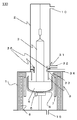
- FIG. 1 is a schematic view showing an example of an apparatus for growing a silicon single crystal by the CZ method of the present invention.
- FIG. 1 illustrates the silicon single crystal growth apparatus 100 by the CZ method
- the present invention can also be applied to a silicon single crystal growth apparatus by the magnetic field application Czochralski method (MCZ method).
- MCZ method magnetic field application Czochralski method
- a graphite crucible 6 for supporting the quartz crucible 5 a heater 7, a heat insulating member 8 and the like are stored.
- the grown silicon single crystal 3 is pulled up and accommodated in the pulling chamber 2.
- the silicon single crystal growth apparatus 100 is provided around the silicon single crystal 3 to be grown, and extends downward from the ceiling of the main chamber 1, and has a substantially cylindrical flow straightening tube 9 that controls the gas flow. Is provided. Further, during the pulling of the silicon single crystal 3, a first gas introduction port 10 for introducing the first gas into the upper portion of the pulling chamber 2 and the first gas so that the atmosphere on the pulling chamber 2 side becomes the first gas. A first gas exhaust port 12 is provided for exhausting the first gas introduced from the introduction port 10 and flowing around the low temperature portion of the silicon single crystal 3 into the rectifying cylinder 9 or upstream from the rectifying cylinder 9.
- the silicon single crystal growing apparatus 100 introduces the second gas into the main chamber 1 so that the atmosphere on the main chamber 1 side is a second gas different from the first gas during the pulling of the silicon single crystal 3.
- a second gas inlet 14 and a second gas outlet 15 provided in the lower part of the main chamber 1 below the second gas inlet 14.
- FIG. 6 is a schematic view of a conventional silicon single crystal growth apparatus 500 using the CZ method.
- a gas inlet 51 is provided in the upper part of the chamber 50 of the silicon single crystal growth apparatus 500, and a gas outlet 52 is provided in the lower part of the chamber 50.
- a desired gas is supplied from the gas inlet 51, and the gas outlet 52 is exhausted by a vacuum pump (not shown).
- a raw material melt 54 which is a silicon melt in a quartz crucible 55, and the oxidizing silicon gas is evaporated from the raw material melt 54 containing oxygen eluted from the quartz crucible.
- This oxidizing silicon gas does not have a strong oxidizing power that oxidizes and weakens the carbon members in the furnace, but if it is not discharged outside the furnace, it accumulates as silicon oxide on the carbon parts in the furnace. It can no longer be used. Therefore, the inert gas introduced from the gas introduction port 51 flows down around the crystal, and further flows over the surface of the raw material melt 54 in the quartz crucible 55 and rises along the crucible wall. A gas flow is formed that passes by the side and leads to a gas outlet 52 connected to a vacuum pump. This flow makes it possible to discharge the oxidizing silicon gas outside the furnace.
- the heat shield member 58 cuts off radiation from the raw material melt 54 and keeps the surface of the raw material melt 54 warm.
- the oxidizing silicon gas evaporated from the raw material melt 4 is combined with the second gas supplied from the second gas inlet 14. While being led to the second gas discharge port 15 at the lower part of the main chamber 1, a part is also led to the first gas discharge port 12.
- the first gas supplied from the first gas inlet 10 at the top of the pulling chamber 2 is discharged from the first gas outlet 12. This makes it possible to make the atmosphere of the second gas on the main chamber 1 side storing the heater 7 and the quartz crucible 5 different from the atmosphere of the first gas on the pulling chamber 2 side.
- the apparatus having such a configuration can control the crystal defects as described above.
- the heat shield member is not installed at the tip of the rectifying cylinder, but a configuration in which the heat shield member is installed is of course applicable.
- the first gas discharge port 12 is connected to a first gas pickup tube 11 in which a plurality of holes 22 are provided at equal intervals in a ring-shaped tube 21 as shown in FIG. It is possible to uniformly collect the atmosphere of the first gas on the side.
- the second gas introduction port 14 is also connected to a second gas supply pipe 13 in which a plurality of holes 26 are provided at equal intervals in a ring-shaped pipe 25 as shown in FIG. It is possible to supply the second gas evenly.
- the first gas discharge port 12 (and the first gas collection tube 11) and the second gas introduction port 14 (and the second gas supply tube 13) are separated from each other.
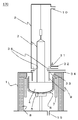
- the first gas outlet 32 and the second gas inlet 34 may be close to each other as in the silicon single crystal growth apparatus 130 shown in FIG. In such a case, by separating the two, it is possible to prevent the second gas introduced from the second gas inlet 34 from being sucked into the first gas outlet 32, and the raw material melt
- the oxidizing silicon gas evaporating from 4 can be exhausted without problems.
- a gas separation plate 36 as shown in FIG. 3 can be provided between the first gas discharge port 32 and the second gas introduction port 34.
- a first gas collection pipe 31 is connected to the first gas discharge port 32
- a second gas supply pipe 33 is connected to the second gas introduction port 34.
- the first gas collection pipe 31 and the second gas supply pipe 33 have the same structure as that shown in FIGS.
- gas separation plate 36 between the first gas exhaust port 32 and the second gas introduction port 34, as in still another silicon single crystal growth apparatus 150 of the present invention shown in FIG. 4.
- gas separation brush 37 may have a brush-like structure by disposing a fibrous member inside the ring-shaped member.
- these members are exposed to high temperatures, quartz materials, carbon materials, silicon carbide, and high melting point metals such as molybdenum, tungsten, and titanium, which are stable at high temperatures, Furthermore, it is preferable to use ceramics that are stable at high temperatures such as boron nitride and alumina. Further, for the member exposed to the oxidizing atmosphere, it is preferable to select and use a material resistant to oxidation in consideration of the use temperature and the oxidation resistance characteristics of each material.
- a mechanism for forming an air curtain with an inert gas such as Ar may be provided between the first gas discharge port 32 and the second gas introduction port 34.
- a plurality of holes are provided inside the ring-shaped tube as in another silicon single crystal growth apparatus 170 of the present invention shown in FIG. 5, and an inert gas is directed toward the silicon single crystal 3.
- An ejecting air curtain forming mechanism 38 can be used.
- the air curtain forming mechanism 38 can have a structure in which a large number of holes are provided inside the ring-shaped tube, like the gas collection tube and the gas supply tube shown in FIG. The effect of separating the atmosphere can be further enhanced.
- the air curtain forming mechanism 38 can also be used in combination with the gas separation plate 36 and the gas separation brush 37.
- the gas atmosphere on the main chamber 1 side in which the heater 7 and the quartz crucible 5 are housed is made an inert gas during single crystal pulling.
- the second gas introduced into the main chamber 1 from the second gas introduction port (14, 34) is an inert gas. If it is an inert gas such as Ar gas that is often used in a conventional single crystal growth apparatus by the CZ method, the heater 7, the quartz crucible 5, and other carbon material parts are deteriorated by oxidation or the like. As usual, it can be used for a long time.
- the first gas introduced into the pulling chamber 2 from the first gas inlet 10 is an oxidizing gas so that the atmosphere on the pulling chamber 2 side is the first gas.
- the atmosphere on the side of the pulling chamber 2 is an oxidizing gas atmosphere, the grown-in defect can be controlled by the above-described I-Si implantation or the like.
- the vacancy As a nitriding atmosphere such as nitrogen gas or ammonia gas It is.
- the temperature of the center part of the silicon single crystal having the same height as the first gas discharge port (12, 32) is 900 ° C. or higher and 1300 ° C. or lower.
- the change in the atmosphere between the first gas outlet and the second gas inlet is preferably on the lower temperature side than about 1300 ° C.
- the control of the Grown-in defect is performed by the diffusion of point defects. Therefore, the effect is reduced when the diffusion coefficient of point defects is small.
- the diffusion coefficient of point defects varies depending on the report, if it is the diffusion coefficient of I-Si, it will decrease by 1 to 3 digits at 900 ° C. compared to 1300 ° C. Therefore, it is preferable that the temperature of the central portion of the silicon single crystal having the same height as the first gas discharge port is 900 ° C. or higher at which a point defect diffusion effect can be sufficiently obtained.
- the temperature of the central portion of the silicon single crystal having the same height as the first gas discharge port 12 is set to 900 ° C. or more by increasing the diameter of the rectifying cylinder 9 as compared with the conventional one. Can do.
- the temperature of the central portion of the silicon single crystal having the same height as the first gas exhaust port (12, 32) is 900 ° C. or higher and 1300 ° C. or lower.
- the target defect is an oxygen precipitate such as BMD (Bulk Micro Defect)
- the temperature at the center of the silicon single crystal at the same height as the first gas outlet (12, 32) is 400 ° C.
- the temperature can be set to a relatively low temperature of 900 ° C. or lower.
- the first gas preferably has an oxygen content of 0.1% to 100% in terms of a flow rate ratio, and components other than oxygen are preferably inert gases.
- the purpose of oxidation is to oxidize the surface of the silicon single crystal 3 and implant I-Si.
- the higher the oxygen concentration the more effective.
- the oxygen concentration is low in terms of deterioration of the carbon member.
- the surface of the silicon single crystal 3 was sufficiently oxidized even when the oxygen concentration was low. Therefore, if oxygen is mixed even at 0.1%, the effect of defect control by the implantation of I-Si is sufficiently exhibited.
- the silicon single crystal 3 in order to prevent the void defect from being generated or eliminated by implanting I-Si, it is more effective to grow the silicon single crystal 3 under the condition that the void defect does not become large.
- Doping nitrogen into the silicon single crystal 3 has an effect of reducing void defects, so doping with nitrogen is more preferable.
- the concentration at which the void defect reduction effect due to nitrogen is exerted is preferably 1 ⁇ 10 11 atoms / cm 3 or more, but when it exceeds 5 ⁇ 10 15 atoms / cm 3 , the silicon single crystal 3 is dislocated due to approaching the solid solution limit. End up. Therefore, the nitrogen concentration in the silicon single crystal 3 is preferably 1 ⁇ 10 11 atoms / cm 3 or more and 5 ⁇ 10 15 atoms / cm 3 or less.
- Example 1 A silicon single crystal 3 was grown using the silicon single crystal growth apparatus 100 of the present invention shown in FIG. At this time, a horizontal magnetic field was applied so that the maximum magnetic field intensity on the crystal central axis was 4000 G.
- the first gas discharge port 12 and the second gas introduction port 14 have the same gas discharge and supply in the cross section of the silicon single crystal growth apparatus 100.
- the first gas collecting pipe 11 and the second gas supply pipe 13 are provided in which a plurality of holes (22, 26) are provided at equal intervals in the ring-shaped pipe (21, 25). Since the first gas collection pipe 11 and the second gas supply pipe 13 are in close contact with the water-cooled chamber, the temperature of the pipe itself is kept relatively low.
- an average crystal growth rate was about 1.0 mm / min, and a silicon single crystal having a diameter of about 10.5 cm was grown with a length of the straight body of about 100 cm.
- the oxygen concentration of the grown silicon single crystal was about 4 ⁇ 10 17 atoms / cm 3 (ASTM'79).
- this single crystal was cut into round pieces, and wafer-like samples were cut out from several places. Each sample was ground and then mirror etched with a mixed acid composed of hydrofluoric acid, nitric acid, and acetic acid.
- the sample was immersed in a selective etching solution composed of hydrofluoric acid, nitric acid, acetic acid, and water, and the sample was left without swinging until the machining allowance by etching became 25 ⁇ 3 ⁇ m on both sides to perform selective etching.
- Example 2 As shown in FIG. 3, the silicon single crystal growth apparatus 130 of the present invention equipped with a quartz gas separation plate 36 as shown in FIG. 3 is used in the single crystal growth apparatus used in Example 1, and the nitrogen concentration in the single crystal is A silicon single crystal was grown under the same conditions as in Example 1 except that nitrogen was doped so as to be in the range of 3 ⁇ 10 13 atoms / cm 3 to 6 ⁇ 10 13 atoms / cm 3 .
- the gas separation plate 36 was confirmed after growing the single crystal, no deterioration due to the oxidizing gas was observed.
- the diameter of the grown silicon single crystal, the length of the straight body, and the actual values of the oxygen concentration were almost the same as those in Example 1.
- Example 1 A silicon single crystal was grown using the conventional silicon single crystal growth apparatus 500 shown in FIG. At this time, a horizontal magnetic field was applied so that the maximum magnetic field intensity on the crystal central axis was 4000 G, and the atmospheric gas was 100% Ar gas. Compared with the silicon single crystal growth apparatus 100 shown in FIG. 1, the silicon single crystal growth apparatus 500 has a large temperature gradient at the crystal growth interface, so that V / G is the same as in the first and second embodiments. A crystal having a diameter of about 10.5 cm was grown with a length of the straight body of about 100 cm at an average crystal growth rate of about 1.2 mm / min, which is faster than that in Example 1. A sample was cut out from this silicon single crystal, and FPD inspection was performed in the same manner as in Example 1.
- FPD was detected in all of the samples cut out from any position. Due to jigs and unevenness during etching, FPD observation at the outermost periphery may lack accuracy, but it is confirmed that FPD exists at least in the region from the outer periphery of the sample to 1.5 cm. It was done.
- the present invention is not limited to the above embodiment.
- the above-described embodiment is an exemplification, and the present invention has substantially the same configuration as the technical idea described in the claims of the present invention, and any device that exhibits the same function and effect is the present invention. It is included in the technical scope of the invention.
Landscapes
- Chemical & Material Sciences (AREA)
- Engineering & Computer Science (AREA)
- Crystallography & Structural Chemistry (AREA)
- Materials Engineering (AREA)
- Metallurgy (AREA)
- Organic Chemistry (AREA)
- Crystals, And After-Treatments Of Crystals (AREA)
Abstract
本発明は、原料融液を収容するルツボ及び原料融液を加熱保温するヒータを格納するメインチャンバと、メインチャンバの上部に連設され、シリコン単結晶が引上げられて収容される引上げチャンバとを有したチョクラルスキー(CZ)法によるシリコン単結晶育成装置であって、シリコン単結晶育成装置は、シリコン単結晶の引上げ中に、引上げチャンバ側の雰囲気を第1ガスとするように、第1ガスを引上げチャンバ内に導入する第1ガス導入口と、第1ガス導入口の下方に設けられた第1ガス排出口とを有し、かつ、メインチャンバ側の雰囲気を第1ガスとは異なる第2ガスとするように、第2ガスをメインチャンバ内に導入する第2ガス導入口と、第2ガス導入口の下方に設けられた第2ガス排出口とを有するシリコン単結晶育成装置である。これにより、CZ法によるシリコン単結晶育成装置において、育成するシリコン単結晶中の欠陥を制御することができるシリコン単結晶育成装置が提供される。
Description
本発明は、チョクラルスキー(CZ)法によるシリコン単結晶育成装置に関する。
近年、デバイスの高集積化に伴い、シリコン単結晶ウェーハへの高品質要求が厳しくなっている。高品質要求とは、デバイスが動作するウェーハ表面近傍の欠陥が少ない、もしくは、無いことである。それらを達成できるウェーハとして、エピタキシャルウェーハ、アニールウェーハ、無欠陥結晶PW(ポリッシュドウェーハ)などがある。
一方で、低コスト化の要求もある。エピタキシャルウェーハやアニールウェーハは、PWに付加工程を加えるものであり、一般に高コストである。結晶成長中に欠陥を制御しながら育成した結晶を、ポリッシュ(研磨)した低欠陥/無欠陥結晶PWは、比較的低コストで高品質要求を満たすことが可能である。このため、Grown-in欠陥を低減した低欠陥結晶PWや、Grown-in欠陥を無くした無欠陥結晶PWの要求が強まっている。
Grown-in欠陥は、点欠陥が結晶成長中に凝集して形成された欠陥である。点欠陥には、格子点のSi原子が欠落したVacancy(空孔)と、格子間にSi原子が入り込んだInterstitial-Si(格子間Si)の2種類が存在する。このGrown-in欠陥の形成状態には、単結晶の成長速度やシリコン融液から引上げられた単結晶の冷却条件により違いが生じる。例えば、成長速度を比較的大きく設定して単結晶を育成した場合には、Vacancyが優勢になることが知られている。このVacancyが凝集して集まったものはVoid欠陥と呼ばれ、検出のされ方によって呼称は異なるが、FPD(Flow Pattern Defect)、COP(Crystal Originated Particle)、あるいは、LSTD(Laser Scattering Tomography Defect)などとして検出される。これらの欠陥がシリコン基板上に形成される酸化膜に取り込まれると、酸化膜の耐圧不良の原因となると考えられている。
一方で、成長速度を比較的低速に設定して単結晶を育成した場合には、Interstitial-Si(以下I-Siと表記することがある)が優勢になることが知られている。このI-Siが凝集すると、転位ループなどがクラスタリングしたと考えられるLEP(Large Etch Pit;転位クラスタ欠陥)が検出される。この転位クラスタ欠陥が生じる領域にデバイスを形成すると、電流リークなど重大な不良を起こすと言われている。
そこで、Vacancyが優勢となる条件とI-Siが優勢となる条件との中間的な条件で結晶を育成すると、VacancyやI-Siが無い、もしくは、Void欠陥や転位クラスタ欠陥を形成しない程度の少量しか存在しない、無欠陥領域が得られる。このような無欠陥結晶の育成方法は、例えば、特許文献1に開示されている。具体的には、結晶成長界面での温度勾配Gと結晶成長速度Vとの比(V/G)を制御することで、無欠陥結晶が得られる。V/Gが大きければVacancy濃度が優勢となり、V/Gが小さいとI-Siが優勢になるので、Vacancy過剰量とI-Si過剰量が拮抗するV/Gに制御することで、点欠陥の過剰量を低減でき、Grown-in欠陥を成長させないようにしている。
しかし、一般に、Grown-in欠陥を成長させないためには精密な制御が必要である上、成長速度も低速化してしまう。このため、一般に、コストは高いものとなってしまう。そこで、結晶の低コスト化が可能な高速で結晶を成長させてVoid欠陥を発生させ、これを消滅させる技術が開示されている。特許文献2には、結晶から切り出したウェーハを非酸化性処理後に酸化処理することで、ウェーハ表層近傍の酸素を外方拡散させた後、表面からI-Siを注入してVoid欠陥を埋める方法が開示されている。
Void欠陥は、Vacancyの集合体であるので、結晶の中に穴の開いたような欠陥である。この穴の内部には、内壁酸化膜と呼ばれる酸化膜が存在していることが知られている。上述の技術では、初めに非酸化性の熱処理を行い、酸素を外方拡散させて酸素濃度を低濃度とし、酸素不足の状態として内壁酸化膜を溶解している。内壁酸化膜が溶解した後に酸化処理を行い、表面に酸化膜を形成することで、I-Siを注入し、内壁酸化膜のないVoid欠陥の穴をI-Siで埋め戻すことで、Void欠陥を消滅させている。
さらに、特許文献3には、低酸素濃度の場合、1200℃以下の酸化処理のみでVoid欠陥が消滅することが開示されている。低酸素であれば、その酸素濃度が平衡濃度となる温度よりも高い温度にすることで、酸素不足の状態になりVoid欠陥の内壁酸化膜が溶解する。そこに、酸化により表面から注入されたI-Siが到達して、Void欠陥が消滅することが開示されている。
さらに、特許文献4では、この技術を応用し、低酸素品ウェーハを酸化処理し、Void欠陥を消滅させている。しかし、これらの技術はいずれも結晶からウェーハを切り出した後、熱処理炉を用いて処理を行う技術である。これらの処理は、結晶成長とは別の工程なので、その分の付加コストがかかってしまい、結局は高コストになってしまうという問題点があった。
また、特許文献5の請求項15には、「真性点欠陥の凝集が起こる温度より高い温度に維持しながらインゴットを酸素雰囲気に暴露する」ことが記載されている。しかし、具体的な方法には触れられておらず、請求項12等から、引上げ後に分離して酸化するものと推定される。つまり、結晶成長後に、インゴット熱処理を別に行なうことが主旨であり、結局は付加工程分のコストがかかってしまう。
上述してきたような酸化処理をもし仮に結晶育成時に行なうことが可能であれば、Grown-in欠陥を結晶育成と同時に消滅させる(もしくは発生させない)ことができる。
一般に、CZ炉内には炭素部品を多く使用している。この炭素部品を多く含むHZ(ホットゾーン)領域では、酸素が混入すると炭素材が酸化してしまい脆くなり、最終的には灰となってしまう。従って、高温で酸化雰囲気に炭素部品を晒すことは出来ない。このため、一般に、CZ法で酸素雰囲気を用いることはなく、先行技術として特許文献6-8がある程度である。
特許文献6に開示された技術は、結晶成長前までルツボ内に酸化性ガスを導入するものであり、特許文献7では、酸素含有雰囲気CZ法でマランゴニ対流を確認しただけであり結晶は育成していない。特許文献8では、水素ガスを導入することを主目的としている。このように、一般的に、CZ法による単結晶育成装置のチャンバ内を酸素含有雰囲気にすることは、HZ領域の部品の劣化の面で、できることではない。
本発明は、上記問題点に鑑みてなされたものであって、CZ法によるシリコン単結晶育成装置において、HZ領域の部品を劣化させることなく、育成するシリコン単結晶中の欠陥を制御することができるシリコン単結晶育成装置を提供することを目的とする。
上記目的を達成するために、本発明は、原料融液を収容するルツボ及び前記原料融液を加熱保温するヒータを格納するメインチャンバと、該メインチャンバの上部に連設され、成長したシリコン単結晶が引上げられて収容される引上げチャンバとを有したチョクラルスキー法によるシリコン単結晶育成装置であって、
前記シリコン単結晶育成装置は、前記シリコン単結晶の引上げ中に、前記引上げチャンバ側の雰囲気を第1ガスとするように、前記第1ガスを前記引上げチャンバ内に導入する第1ガス導入口と、前記第1ガス導入口の下方に設けられた第1ガス排出口とを有するものであり、かつ、
前記シリコン単結晶育成装置は、前記シリコン単結晶の引上げ中に、前記メインチャンバ側の雰囲気を前記第1ガスとは異なる第2ガスとするように、前記第2ガスを前記メインチャンバ内に導入する第2ガス導入口と、前記第2ガス導入口の下方に設けられた第2ガス排出口とを有するものであることを特徴とするシリコン単結晶育成装置を提供する。
前記シリコン単結晶育成装置は、前記シリコン単結晶の引上げ中に、前記引上げチャンバ側の雰囲気を第1ガスとするように、前記第1ガスを前記引上げチャンバ内に導入する第1ガス導入口と、前記第1ガス導入口の下方に設けられた第1ガス排出口とを有するものであり、かつ、
前記シリコン単結晶育成装置は、前記シリコン単結晶の引上げ中に、前記メインチャンバ側の雰囲気を前記第1ガスとは異なる第2ガスとするように、前記第2ガスを前記メインチャンバ内に導入する第2ガス導入口と、前記第2ガス導入口の下方に設けられた第2ガス排出口とを有するものであることを特徴とするシリコン単結晶育成装置を提供する。
このように、引上げチャンバ側の雰囲気を第1ガスとし、メインチャンバ側の雰囲気を第2ガスとすることができるシリコン単結晶育成装置であれば、シリコン単結晶育成装置のHZ領域の部品を劣化させずに、所望雰囲気で育成するシリコン単結晶中の欠陥を制御することができる。
このとき、前記シリコン単結晶育成装置は、さらに、
育成するシリコン単結晶の周囲に設けられ、前記メインチャンバの天井部から下方に延設された円筒状の整流筒を有するものであることが好ましい。
育成するシリコン単結晶の周囲に設けられ、前記メインチャンバの天井部から下方に延設された円筒状の整流筒を有するものであることが好ましい。
このような整流筒を設けることにより、育成されるシリコン単結晶の周囲のガスの流れを制御し、原料融液から蒸発する酸化性シリコンガスを効果的に排出することができるとともに、第1ガスと第2ガスとの雰囲気を分離し易くなる。
このとき、前記シリコン単結晶育成装置は、さらに、
前記第1ガス排出口と前記第2ガス導入口の間に、ガス分離板、又はガス分離ブラシが設けられたものであり、
前記ガス分離板及び前記ガス分離ブラシは、石英材、炭素材、炭化珪素、高融点金属、及びセラミックスのいずれか一つ以上からなることが好ましい。
前記第1ガス排出口と前記第2ガス導入口の間に、ガス分離板、又はガス分離ブラシが設けられたものであり、
前記ガス分離板及び前記ガス分離ブラシは、石英材、炭素材、炭化珪素、高融点金属、及びセラミックスのいずれか一つ以上からなることが好ましい。
このようにガス分離板又はガス分離ブラシを設けることにより、第1ガスの雰囲気と第2ガスの雰囲気をさらに効果的に分離することができ、第2ガス導入口から導入された第2ガスが第1ガス排出口に吸い込まれるのを防ぎ、メインチャンバ側の雰囲気を確実に第2ガスとすることができる。また、ガス分離板及びガス分離ブラシが上記のような材料であれば、高温に晒されても安定であり、劣化が起こりにくくすることができる。
このとき、前記シリコン単結晶育成装置は、さらに、
前記第1ガス排出口と前記第2ガス導入口の間に、不活性ガスによるエアカーテンを形成する機構を有するものであることが好ましい。
前記第1ガス排出口と前記第2ガス導入口の間に、不活性ガスによるエアカーテンを形成する機構を有するものであることが好ましい。
このように、エアカーテンを形成する機構を設ければ、第1ガス排出口と第2ガス導入口の間をより確実に分離し、第2ガスが第1ガス排出口に吸い込まれるのを防ぐことができ、メインチャンバ側の雰囲気を確実に第2ガスとすることができる。
このとき、前記第2ガスが不活性ガスであることが好ましい。
このように第2ガスを不活性ガスとすれば、ヒータ、ルツボ、さらには、その他の炭素材部品等が酸化等により劣化することがなく、長時間使用することができる。
このとき、前記第1ガスが酸化性ガスであることが好ましい。
このように、第1ガスを酸化性ガスとすることにより、引上げチャンバ側の雰囲気を酸化性ガスとすることができ、育成したシリコン単結晶の表面を酸化することにより、I-Siの注入などでGrown-in欠陥の制御を行うことができる。
このとき、前記第1ガス排出口と同じ高さの前記シリコン単結晶の中心部の温度が、900℃以上1300℃以下となるものであることが好ましい。
このような温度範囲であれば、効果的にGrown-in欠陥の制御を行うことができ、かつ、HZ領域の部品の劣化を抑制することができる。
このとき、前記第1ガスは、酸素含有量が流量比で0.1%以上100%以下であり、酸素以外の成分は不活性ガスであることが好ましい。
このような酸素含有量の範囲であれば、育成するシリコン単結晶の表面を確実に酸化することができ、シリコン単結晶中の欠陥を制御することができる。
以上のように、本発明によれば、シリコン単結晶育成後に追加の熱処理工程を必要とせず、かつ、HZ領域の部品の劣化も抑えつつ、育成するシリコン単結晶中の欠陥を制御することができる。
以下、本発明をより詳細に説明する。
上記のように、チョクラルスキー法によるシリコン単結晶育成装置において、育成するシリコン単結晶の欠陥を制御することができるシリコン単結晶育成装置が求められている。
本発明者らは、上記目的を達成するために鋭意検討を行った結果、チョクラルスキー法によるシリコン単結晶育成装置であって、
シリコン単結晶の引上げ中に、引上げチャンバ側の雰囲気を第1ガスとするように、第1ガスを引上げチャンバ内に導入する第1ガス導入口と、第1ガス導入口の下方に設けられた第1ガス排出口とを有するものであり、かつ、
メインチャンバ側の雰囲気を第1ガスとは異なる第2ガスとするように、第2ガスをメインチャンバ内に導入する第2ガス導入口と、第2ガス導入口の下方に設けられた第2ガス排出口とを有するものであることを特徴とするシリコン単結晶育成装置が、上記課題を解決できることを見出し、本発明を完成させた。
シリコン単結晶の引上げ中に、引上げチャンバ側の雰囲気を第1ガスとするように、第1ガスを引上げチャンバ内に導入する第1ガス導入口と、第1ガス導入口の下方に設けられた第1ガス排出口とを有するものであり、かつ、
メインチャンバ側の雰囲気を第1ガスとは異なる第2ガスとするように、第2ガスをメインチャンバ内に導入する第2ガス導入口と、第2ガス導入口の下方に設けられた第2ガス排出口とを有するものであることを特徴とするシリコン単結晶育成装置が、上記課題を解決できることを見出し、本発明を完成させた。
以下、本発明について、実施態様の一例として、図を参照しながら詳細に説明するが、本発明はこれに限定されるものではない。
まず、図1を参照して、本発明のシリコン単結晶育成装置について説明する。図1は、本発明のCZ法によるシリコン単結晶育成装置の一例を示す概略図である。図1では、CZ法によるシリコン単結晶育成装置100を例示したが、本発明は、磁場印加チョクラルスキー法(MCZ法)によるシリコン単結晶育成装置にも適用することができる。
図1に示したシリコン単結晶育成装置100は、メインチャンバ1と引上げチャンバ2を備えている。メインチャンバ1内には、原料融液4を収容する石英ルツボ5、石英ルツボ5を支持する黒鉛ルツボ6、加熱ヒータ7、及び、断熱部材8等が格納されている。一方、引上げチャンバ2内には、成長したシリコン単結晶3が引上げられて収容される。
また、シリコン単結晶育成装置100は、育成されるシリコン単結晶3の周囲に設けられ、メインチャンバ1の天井部から下方に延設された、ガスの流れを制御する略円筒状の整流筒9を備える。さらに、シリコン単結晶3の引上げ中に、引上げチャンバ2側の雰囲気を第1ガスとするように、引上げチャンバ2の上部に、第1ガスを導入する第1ガス導入口10と、第1ガス導入口10から導入され、シリコン単結晶3の低温部の周囲を流下する第1ガスを、整流筒9中、もしくは整流筒9より上流で排気する第1ガス排出口12を備えている。
さらに、シリコン単結晶育成装置100は、シリコン単結晶3の引上げ中に、メインチャンバ1側の雰囲気を第1ガスとは異なる第2ガスとするように、第2ガスをメインチャンバ1内に導入する第2ガス導入口14と、第2ガス導入口14の下方で、メインチャンバ1の下部に設けられた第2ガス排出口15とを備える。
ここで、一般的なシリコン単結晶育成装置内のガスの流れを、図6を参照して説明する。
図6は、従来のCZ法によるシリコン単結晶育成装置500の概略図である。シリコン単結晶育成装置500のチャンバ50の上部にはガス導入口51が設けられ、チャンバ50の下部にはガス排出口52が設けられている。そして、ガス導入口51からは所望のガスが供給され、ガス排出口52は真空ポンプ(不図示)により排気されている。チャンバ50内には、石英ルツボ55内にシリコンの溶融液である原料融液54があり、石英ルツボから溶出した酸素を含む原料融液54から酸化性シリコンガスが蒸発している。
この酸化性シリコンガスには炉内の炭素部材を酸化して脆くするような強い酸化力はないが、炉外に排出しないと、炉内の炭素部品等に酸化シリコンとして堆積し、炭素部品が使用できなくなってしまう。そこで、ガス導入口51から導入された不活性ガスを結晶の周囲に流下し、さらに、石英ルツボ55内の原料融液54の表面上を流れ、ルツボ壁に沿って上昇し、加熱ヒータ57の脇を通過して、真空ポンプにつながれたガス排出口52へと導くガスの流れを形成している。この流れにより、酸化性シリコンガスを炉外に排出することが可能となっている。尚、遮熱部材58は、原料融液54からの輻射をカットするとともに、原料融液54の表面を保温している。
これに対し、図1に概略図を示した本発明のシリコン単結晶育成装置100では、原料融液4から蒸発する酸化性シリコンガスは第2ガス導入口14から供給された第2ガスと共に、メインチャンバ1の下部の第2ガス排出口15に導かれると共に、一部は第1ガス排出口12にも導かれる。その一方で、引上げチャンバ2の上部の第1ガス導入口10から供給された第1ガスは、第1ガス排出口12で排出される。これにより、加熱ヒータ7及び石英ルツボ5を格納したメインチャンバ1側の第2ガスの雰囲気と、引上げチャンバ2側の第1ガスの雰囲気とを異なった雰囲気とすることが可能となる。この様な構成の装置により、上述してきたような結晶欠陥の制御を行なうことができる。図1では整流筒の先端に遮熱部材が設置されていないが、遮熱部材が設置された構成ももちろん適用可能である。
このとき、第1ガス排出口12は、図2(a)に示すような、リング状の管21に複数の孔22を均等間隔に設けた第1ガス収拾管11と接続され、引上げチャンバ2側の第1ガスの雰囲気を均等に収拾することを可能とする。また、第2ガス導入口14も、図2(b)に示すような、リング状の管25に複数の孔26を均等間隔に設けた第2ガス供給管13と接続され、メインチャンバ1内に第2ガスを均等に供給することを可能とする。
次に、本発明の他のシリコン単結晶育成装置について、図3を参照して説明する。
図1に例示したシリコン単結晶育成装置100では、第1ガス排出口12(及び第1ガス収拾管11)と第2ガス導入口14(及び第2ガス供給管13)との間を離してあるが、設計によっては、図3に示したシリコン単結晶育成装置130の様に、第1ガス排出口32と第2ガス導入口34とが接近している場合もある。このような場合、両者の間を分離することによって、第2ガス導入口34から導入された第2ガスが、第1ガス排出口32に吸い込まれてしまうことを防ぐことができ、原料融液4から蒸発する酸化性シリコンガスの排気を問題なく行うことができる。具体的な分離手段としては、第1ガス排出口32と第2ガス導入口34との間に、図3に示したようなガス分離板36を設けることができる。尚、図3においては、第1ガス排出口32には第1ガス収拾管31が、第2ガス導入口34には第2ガス供給管33が接続されている。第1ガス収拾管31及び第2ガス供給管33は、図2(a)及び(b)に示したのと同様な構造を有している。
また、図3に示したガス分離板36の代わりに、図4に示す本発明のさらに他のシリコン単結晶育成装置150のように、第1ガス排出口32と第2ガス導入口34の間に、ガス分離ブラシ37を設けた構造とすることもできる。ガス分離ブラシ37は、リング状部材の内側に繊維状の部材を配置してブラシのような構造としたものとすることができる。
このとき、これらの部材(ガス分離板36及びガス分離ブラシ37)は高温に晒されるので、高温で安定な石英材、炭素材、炭化珪素、及び、モリブデン、タングステン、チタンなどの高融点金属、さらには、窒化ボロン、アルミナなどの高温で安定なセラミックスなどを用いることが好ましい。さらに、酸化性の雰囲気に晒される部材については、使用温度と各材質の耐酸化特性を考慮して、酸化に強い材質を選別して用いることが好ましい。
また、さらに他の分離手段として、第1ガス排出口32と第2ガス導入口34との間に、Ar等の不活性ガスによるエアカーテンを形成する機構を設けることもできる。具体的には、図5に示す、本発明のさらに他のシリコン単結晶育成装置170のように、リング状の管の内側に複数の孔を設け、シリコン単結晶3に向って不活性ガスを噴出するエアカーテン形成機構38を用いることができる。エアカーテン形成機構38は、図2に示したガス収拾管やガス供給管と同様に、リング状の管の内側に多数の孔を設けた構造とすることができるが、孔の間隔を小さくすると雰囲気の分離効果をより高めることができる。また、エアカーテン形成機構38は、ガス分離板36やガス分離ブラシ37と併用することもできる。
次に、本発明のシリコン単結晶育成装置を稼働させるうえでの特徴について説明する。本発明のシリコン単結晶育成装置(100、130、150、170)では、単結晶引き上げ中に、加熱ヒータ7及び石英ルツボ5を格納するメインチャンバ1側のガス雰囲気を不活性ガスとすることが好ましい。このため、第2ガス導入口(14、34)からメインチャンバ1内に導入される第2ガスは、不活性ガスであることが好ましい。従来のCZ法による単結晶育成装置で用いられることの多いArガスのような不活性ガスであれば、加熱ヒータ7や石英ルツボ5、さらには、その他の炭素材部品等が酸化等により劣化することがなく、従来通り、長時間使用可能である。
また、引上げチャンバ2側の雰囲気を第1ガスとするように、第1ガス導入口10から引上げチャンバ2内に導入される第1ガスを、酸化性ガスとすることが好ましい。引上げチャンバ2側の雰囲気を酸化性ガス雰囲気とすることで、先に述べたようなI-Siの注入などによりGrown-in欠陥の制御を行なうことができる。
引上げチャンバ2側の第1ガスの雰囲気による欠陥の制御としては、酸化性ガスによるI-Siの注入の他に、窒素ガスやアンモニアガスなどの窒化性の雰囲気として、Vacancyを注入することも可能である。
また、第1ガス排出口(12、32)と同じ高さのシリコン単結晶の中心部の温度が、900℃以上1300℃以下であることが好ましい。
Grown-in欠陥は点欠陥の拡散によって形成される。このため、Void欠陥が形成されてしまう温度より高い温度でI-Siの注入を行なえば、Void欠陥そのものが形成されないので、より高温で第2ガスから第1ガスへ雰囲気を変えることが好ましい。しかしながら、炭素部材がある付近では不活性ガス雰囲気にしないと部品が劣化するので、結晶成長界面付近では不活性ガス雰囲気としたい。このとき、1300℃以下であれば、HZ領域の部品の劣化は生じにくい。従って、第1ガス排出口と第2ガス導入口の間での雰囲気の変更は1300℃程度より低温側が好ましい。
一方で、Grown-in欠陥の制御は点欠陥の拡散により行なわれる。従って、点欠陥の拡散係数が小さいと効果が低下する。点欠陥の拡散係数も報告によってばらつきはあるが、I-Siの拡散係数であれば、1300℃に比較して900℃では1~3桁低下してしまう。従って、第1ガス排出口と同じ高さのシリコン単結晶の中心部の温度は点欠陥の拡散効果が十分に得られる900℃以上とすることが好ましい。このとき、例えば図1に示すように、整流筒9の口径を従来より大きくすることにより、第1ガス排出口12と同じ高さのシリコン単結晶の中心部の温度を900℃以上にすることができる。
上述のように、Grown-in欠陥に関しては、第1ガス排出口(12、32)と同じ高さのシリコン単結晶の中心部の温度が、900℃以上1300℃以下とするのが好適である。しかし、対象となる欠陥がBMD(Bulk Micro Defect)のような酸素析出物の場合には、第1ガス排出口(12、32)と同じ高さのシリコン単結晶の中心部の温度は400℃以上900℃以下の比較的低い温度とすることができる。
また、第1ガスは、酸素含有量が流量比で0.1%以上100%以下であり、酸素以外の成分は不活性ガスであることが好ましい。
酸化する目的は、シリコン単結晶3の表面を酸化してI-Siを注入することである。酸化のためには、酸素濃度が高いほど効果がある。しかし、引上げチャンバ2側とメインチャンバ1側で雰囲気の切り替えを行っても、若干の酸化性ガスの漏れが生じる可能性があるので、炭素部材の劣化の面からは酸素濃度が薄いほうが好ましい。実際には、酸素濃度が低くてもシリコン単結晶3の表面の酸化は十分に起こった。従って、0.1%でも酸素が混ざっていれば、I-Siの注入による欠陥制御の効果が十分に発揮される。
また、I-Siを注入して、Void欠陥を発生させない、又は、消滅させるためには、Void欠陥が大きくならない条件でシリコン単結晶3を育成した方が、効果が現れやすい。シリコン単結晶3に窒素をドープすることで、Void欠陥を小さくする効果があるので、窒素をドープすることがより好ましい。窒素によるVoid欠陥縮小の効果がでる濃度としては、1×10¹¹atoms/cm3以上が好ましいが、5×1015atoms/cm3を超えると固溶限に近づきシリコン単結晶3が有転位化してしまう。従って、シリコン単結晶3中の窒素濃度は、1×1011atoms/cm3以上5×1015atoms/cm3以下とすることが好ましい。
以下、実施例及び比較例を示して本発明をより具体的に説明するが、本発明はこれらに限定されるものではない。
(実施例1)
図1に示した本発明のシリコン単結晶育成装置100を用いて、シリコン単結晶3を育成した。このとき、結晶中心軸上の最大磁場強度が4000Gとなる様に水平磁場を印加した。第1ガス排出口12と第2ガス導入口14には、シリコン単結晶育成装置100の断面内のガス排出及び供給を均一化するため、図2(a)及び(b)に示したような、リング状の管(21、25)に複数の孔(22、26)を均等間隔に設けた第1ガス収拾管11及び第2ガス供給管13を設けてある。これらの第1ガス収拾管11及び第2ガス供給管13は水冷されたチャンバに密着しているので、管自体の温度は比較的低温に保たれている。そして、第1ガス供給口10からは酸素を3%含んだArガスを供給した。一方で、第2ガス導入口14からは100%Arガスを供給した。第1ガス排出口12に繋がる第1ガス収拾管11と同じ高さの結晶の中心部の温度は、総合伝熱解析ソフトFEMAGにて解析したところ、およそ1170℃であった。
図1に示した本発明のシリコン単結晶育成装置100を用いて、シリコン単結晶3を育成した。このとき、結晶中心軸上の最大磁場強度が4000Gとなる様に水平磁場を印加した。第1ガス排出口12と第2ガス導入口14には、シリコン単結晶育成装置100の断面内のガス排出及び供給を均一化するため、図2(a)及び(b)に示したような、リング状の管(21、25)に複数の孔(22、26)を均等間隔に設けた第1ガス収拾管11及び第2ガス供給管13を設けてある。これらの第1ガス収拾管11及び第2ガス供給管13は水冷されたチャンバに密着しているので、管自体の温度は比較的低温に保たれている。そして、第1ガス供給口10からは酸素を3%含んだArガスを供給した。一方で、第2ガス導入口14からは100%Arガスを供給した。第1ガス排出口12に繋がる第1ガス収拾管11と同じ高さの結晶の中心部の温度は、総合伝熱解析ソフトFEMAGにて解析したところ、およそ1170℃であった。
このシリコン単結晶育成装置100を用いて、平均の結晶成長速度を約1.0mm/minとして、直径約10.5cmのシリコン単結晶を直胴部の長さ約100cmで育成した。操業後に確認したところ、炉内の炭素材部品が酸化されることはなかった。育成されたシリコン単結晶の酸素濃度は、約4×1017atoms/cm3(ASTM’79)であった。次に、この単結晶を輪切りにして、数箇所からウェーハ状のサンプルを切り出した。この各サンプルを平面研削した後、フッ酸、硝酸、酢酸からなる混酸でミラーエッチングした。さらに、フッ酸、硝酸、酢酸、水からなる選択性のあるエッチング液にサンプルを浸し、エッチングによる取り代が両側で25±3μmになるまで揺動せずに放置し、選択エッチングを行った。
その後、選択エッチングを行ったサンプルを光学顕微鏡にて観察した結果、FPDは各サンプルの中心部にのみ検出された。FPDが検出された直径はサンプルによって異なるが、3~6cm程度であった。このことから、サンプルの周辺部から一定範囲のVoid欠陥が消滅したことが分かった。シリコン単結晶の引上げ工程において、点欠陥(I-Si)の拡散時間を延ばすように高温の熱履歴を工夫したり、より高温まで酸化したりといった条件のチューニングを実施すれば、全面のVoid欠陥を消滅可能と推察された。
(実施例2)
実施例1で用いた単結晶育成装置に図3に示したような、石英製のガス分離板36を装着した本発明のシリコン単結晶育成装置130を用い、また、単結晶中の窒素濃度が3×10¹³atoms/cm3から6×1013atoms/cm3の範囲となるように、窒素をドープしたことを除いては、実施例1と同じ条件でシリコン単結晶を育成した。単結晶育成後にガス分離板36を確認したところ、酸化性ガスに起因するような劣化は見られなかった。育成されたシリコン単結晶の直径、直胴部の長さ、酸素濃度の実績値も実施例1とほぼ同等であった。
実施例1で用いた単結晶育成装置に図3に示したような、石英製のガス分離板36を装着した本発明のシリコン単結晶育成装置130を用い、また、単結晶中の窒素濃度が3×10¹³atoms/cm3から6×1013atoms/cm3の範囲となるように、窒素をドープしたことを除いては、実施例1と同じ条件でシリコン単結晶を育成した。単結晶育成後にガス分離板36を確認したところ、酸化性ガスに起因するような劣化は見られなかった。育成されたシリコン単結晶の直径、直胴部の長さ、酸素濃度の実績値も実施例1とほぼ同等であった。
このシリコン単結晶からサンプルを切り出し、実施例1と同様の処理を行った後、実施例1と同条件でFPD検査を行った。その結果、どの位置から切り出したサンプルも、面内の全てでFPDは検出されなかった。これは窒素ドープにより、Void欠陥成長が抑制された効果と酸化により、I-Siの注入効果の両方の効果が寄与したと考えられる。
(比較例1)
図6に示した従来のシリコン単結晶育成装置500を用いて、シリコン単結晶を育成した。このとき、結晶中心軸上の最大磁場強度が4000Gとなる様に水平磁場を印加し、雰囲気ガスはArガス100%とした。図1に示したシリコン単結晶育成装置100と比較して、シリコン単結晶育成装置500では、結晶成長界面での温度勾配が大きいので、V/Gが実施例1、2と同じになるように実施例1よりも速い、平均の結晶成長速度約1.2mm/minとして、直径約10.5cmの結晶を直胴部の長さ約100cmで育成した。このシリコン単結晶からサンプルを切り出し、実施例1と同様にしてFPD検査を行った。その結果、どの位置から切り出したサンプルも、面内の全てでFPDが検出された。エッチング時の治具やムラなどに起因して、最外周のFPD観察は正確性を欠くことがあるが、少なくとも、サンプルの外周から1.5cmまでの領域ではFPDが存在していることが確認された。
図6に示した従来のシリコン単結晶育成装置500を用いて、シリコン単結晶を育成した。このとき、結晶中心軸上の最大磁場強度が4000Gとなる様に水平磁場を印加し、雰囲気ガスはArガス100%とした。図1に示したシリコン単結晶育成装置100と比較して、シリコン単結晶育成装置500では、結晶成長界面での温度勾配が大きいので、V/Gが実施例1、2と同じになるように実施例1よりも速い、平均の結晶成長速度約1.2mm/minとして、直径約10.5cmの結晶を直胴部の長さ約100cmで育成した。このシリコン単結晶からサンプルを切り出し、実施例1と同様にしてFPD検査を行った。その結果、どの位置から切り出したサンプルも、面内の全てでFPDが検出された。エッチング時の治具やムラなどに起因して、最外周のFPD観察は正確性を欠くことがあるが、少なくとも、サンプルの外周から1.5cmまでの領域ではFPDが存在していることが確認された。
このように、本発明のシリコン単結晶育成装置を用いてシリコン単結晶の育成を行った場合、欠陥が全く検出されないか、又は、中心部のごく限られた領域のみに欠陥が発生していた。これに対し、従来のシリコン単結晶育成装置を用いてシリコン単結晶の育成を行った場合は、全面に欠陥が発生していた。
なお、本発明は、上記実施形態に限定されるものではない。上記実施形態は、例示であり、本発明の特許請求の範囲に記載された技術的思想と実質的に同一な構成を有し、同様な作用効果を奏するものは、いかなるものであっても本発明の技術的範囲に包含される。
Claims (8)
- 原料融液を収容するルツボ及び前記原料融液を加熱保温するヒータを格納するメインチャンバと、該メインチャンバの上部に連設され、成長したシリコン単結晶が引上げられて収容される引上げチャンバとを有したチョクラルスキー法によるシリコン単結晶育成装置であって、
前記シリコン単結晶育成装置は、前記シリコン単結晶の引上げ中に、前記引上げチャンバ側の雰囲気を第1ガスとするように、前記第1ガスを前記引上げチャンバ内に導入する第1ガス導入口と、前記第1ガス導入口の下方に設けられた第1ガス排出口とを有するものであり、かつ、
前記シリコン単結晶育成装置は、前記シリコン単結晶の引上げ中に、前記メインチャンバ側の雰囲気を前記第1ガスとは異なる第2ガスとするように、前記第2ガスを前記メインチャンバ内に導入する第2ガス導入口と、前記第2ガス導入口の下方に設けられた第2ガス排出口とを有するものであることを特徴とするシリコン単結晶育成装置。 - 前記シリコン単結晶育成装置は、さらに、
育成するシリコン単結晶の周囲に設けられ、前記メインチャンバの天井部から下方に延設された円筒状の整流筒を有するものであることを特徴とする請求項1に記載のシリコン単結晶育成装置。 - 前記シリコン単結晶育成装置は、さらに、
前記第1ガス排出口と前記第2ガス導入口の間に、ガス分離板、又はガス分離ブラシが設けられたものであり、
前記ガス分離板及び前記ガス分離ブラシは、石英材、炭素材、炭化珪素、高融点金属、及びセラミックスのいずれか一つ以上からなることを特徴とする請求項1又は請求項2に記載のシリコン単結晶育成装置。 - 前記シリコン単結晶育成装置は、さらに、
前記第1ガス排出口と前記第2ガス導入口の間に、不活性ガスによるエアカーテンを形成する機構を有するものであることを特徴とする請求項1から請求項3のいずれか一項に記載のシリコン単結晶育成装置。 - 前記第2ガスが不活性ガスであることを特徴とする請求項1から請求項4のいずれか一項に記載のシリコン単結晶育成装置。
- 前記第1ガスが酸化性ガスであることを特徴とする請求項1から請求項5のいずれか一項に記載のシリコン単結晶育成装置。
- 前記第1ガス排出口と同じ高さの前記シリコン単結晶の中心部の温度が、900℃以上1300℃以下となるものであることを特徴とする請求項1から請求項6のいずれか一項に記載のシリコン単結晶育成装置。
- 前記第1ガスは、酸素含有量が流量比で0.1%以上100%以下であり、酸素以外の成分は不活性ガスであることを特徴とする請求項1から請求項7のいずれか一項に記載のシリコン単結晶育成装置。
Applications Claiming Priority (2)
| Application Number | Priority Date | Filing Date | Title |
|---|---|---|---|
| JP2015149885A JP6287991B2 (ja) | 2015-07-29 | 2015-07-29 | シリコン単結晶育成装置 |
| JP2015-149885 | 2015-07-29 |
Publications (1)
| Publication Number | Publication Date |
|---|---|
| WO2017017893A1 true WO2017017893A1 (ja) | 2017-02-02 |
Family
ID=57884321
Family Applications (1)
| Application Number | Title | Priority Date | Filing Date |
|---|---|---|---|
| PCT/JP2016/003091 Ceased WO2017017893A1 (ja) | 2015-07-29 | 2016-06-28 | シリコン単結晶育成装置 |
Country Status (2)
| Country | Link |
|---|---|
| JP (1) | JP6287991B2 (ja) |
| WO (1) | WO2017017893A1 (ja) |
Cited By (2)
| Publication number | Priority date | Publication date | Assignee | Title |
|---|---|---|---|---|
| CN112899772A (zh) * | 2019-11-19 | 2021-06-04 | Ftb研究所株式会社 | 单晶生长装置、该单晶生长装置的使用方法及单晶 |
| CN116103757A (zh) * | 2023-03-08 | 2023-05-12 | 隆基绿能科技股份有限公司 | 一种单晶硅棒拉制方法和单晶硅棒拉制装置 |
Citations (4)
| Publication number | Priority date | Publication date | Assignee | Title |
|---|---|---|---|---|
| JPH09142990A (ja) * | 1995-11-28 | 1997-06-03 | Mitsubishi Materials Corp | シリコン単結晶中の酸素濃度の低減方法及びその装置 |
| JP2003517412A (ja) * | 1998-06-26 | 2003-05-27 | エムイーエムシー・エレクトロニック・マテリアルズ・インコーポレイテッド | 任意に大きい直径を有する無欠陥シリコン結晶の成長方法 |
| JP2004217460A (ja) * | 2003-01-14 | 2004-08-05 | Sumitomo Mitsubishi Silicon Corp | 水素ドープシリコン単結晶製造方法 |
| JP2007254165A (ja) * | 2006-03-20 | 2007-10-04 | Toshiba Ceramics Co Ltd | 単結晶引上装置 |
-
2015
- 2015-07-29 JP JP2015149885A patent/JP6287991B2/ja active Active
-
2016
- 2016-06-28 WO PCT/JP2016/003091 patent/WO2017017893A1/ja not_active Ceased
Patent Citations (4)
| Publication number | Priority date | Publication date | Assignee | Title |
|---|---|---|---|---|
| JPH09142990A (ja) * | 1995-11-28 | 1997-06-03 | Mitsubishi Materials Corp | シリコン単結晶中の酸素濃度の低減方法及びその装置 |
| JP2003517412A (ja) * | 1998-06-26 | 2003-05-27 | エムイーエムシー・エレクトロニック・マテリアルズ・インコーポレイテッド | 任意に大きい直径を有する無欠陥シリコン結晶の成長方法 |
| JP2004217460A (ja) * | 2003-01-14 | 2004-08-05 | Sumitomo Mitsubishi Silicon Corp | 水素ドープシリコン単結晶製造方法 |
| JP2007254165A (ja) * | 2006-03-20 | 2007-10-04 | Toshiba Ceramics Co Ltd | 単結晶引上装置 |
Cited By (3)
| Publication number | Priority date | Publication date | Assignee | Title |
|---|---|---|---|---|
| CN112899772A (zh) * | 2019-11-19 | 2021-06-04 | Ftb研究所株式会社 | 单晶生长装置、该单晶生长装置的使用方法及单晶 |
| CN112899772B (zh) * | 2019-11-19 | 2024-04-05 | Ftb研究所株式会社 | 单晶生长装置、该单晶生长装置的使用方法及单晶 |
| CN116103757A (zh) * | 2023-03-08 | 2023-05-12 | 隆基绿能科技股份有限公司 | 一种单晶硅棒拉制方法和单晶硅棒拉制装置 |
Also Published As
| Publication number | Publication date |
|---|---|
| JP6287991B2 (ja) | 2018-03-07 |
| JP2017030991A (ja) | 2017-02-09 |
Similar Documents
| Publication | Publication Date | Title |
|---|---|---|
| JP5515406B2 (ja) | シリコンウェーハおよびその製造方法 | |
| KR101684873B1 (ko) | 실리콘 기판의 제조 방법 및 실리콘 기판 | |
| US20200141024A1 (en) | N-type silicon single crystal production method, n-type silicon single crystal ingot, silicon wafer, and epitaxial silicon wafer | |
| CN100342503C (zh) | 退火晶片及退火晶片的制造方法 | |
| JP6971622B2 (ja) | 半導体ウェハの製造方法及び半導体ウェハ | |
| KR101313462B1 (ko) | 실리콘 웨이퍼의 열처리 방법 | |
| CN110678585A (zh) | 单晶硅锭的制造方法及单晶硅培育装置 | |
| JP4853237B2 (ja) | エピタキシャルウェーハの製造方法 | |
| JP4661204B2 (ja) | 単結晶の製造方法およびアニールウェーハの製造方法ならびにアニールウェーハ | |
| JP5636168B2 (ja) | シリコン単結晶の育成方法 | |
| JP6287991B2 (ja) | シリコン単結晶育成装置 | |
| WO2006117939A1 (ja) | シリコンウェーハの製造方法 | |
| KR102765624B1 (ko) | 탄소도프 실리콘 단결정 웨이퍼 및 그의 제조방법 | |
| JP2005142434A (ja) | シリコン単結晶ウェーハの製造方法及びシリコン単結晶ウェーハ | |
| JP6413970B2 (ja) | シリコン単結晶の育成方法 | |
| JP5262021B2 (ja) | シリコンウェーハ及びその製造方法 | |
| JP5489064B2 (ja) | シリコン単結晶の育成方法 | |
| KR101658892B1 (ko) | 웨이퍼의 열처리 방법 및 실리콘 웨이퍼의 제조 방법 및 실리콘 웨이퍼 및 열처리 장치 | |
| JP2010040588A (ja) | シリコンウェーハ | |
| JP5428608B2 (ja) | シリコン単結晶の育成方法 | |
| JP5583053B2 (ja) | シリコンウェーハの熱処理方法 | |
| CN113862791A (zh) | 一种用于拉制单晶硅棒的拉晶炉 | |
| JP2011054655A (ja) | 高周波デバイス向けシリコンウェーハおよびその製造方法 | |
| JP6845020B2 (ja) | シリコンウェーハの熱処理方法 | |
| JP2010202436A (ja) | 単結晶引き上げ装置 |
Legal Events
| Date | Code | Title | Description |
|---|---|---|---|
| 121 | Ep: the epo has been informed by wipo that ep was designated in this application |
Ref document number: 16830002 Country of ref document: EP Kind code of ref document: A1 |
|
| NENP | Non-entry into the national phase |
Ref country code: DE |
|
| 122 | Ep: pct application non-entry in european phase |
Ref document number: 16830002 Country of ref document: EP Kind code of ref document: A1 |