WO2017013768A1 - 半導体装置 - Google Patents
半導体装置 Download PDFInfo
- Publication number
- WO2017013768A1 WO2017013768A1 PCT/JP2015/070834 JP2015070834W WO2017013768A1 WO 2017013768 A1 WO2017013768 A1 WO 2017013768A1 JP 2015070834 W JP2015070834 W JP 2015070834W WO 2017013768 A1 WO2017013768 A1 WO 2017013768A1
- Authority
- WO
- WIPO (PCT)
- Prior art keywords
- semiconductor chip
- transformer
- inductor
- chip
- semiconductor device
- Prior art date
- Legal status (The legal status is an assumption and is not a legal conclusion. Google has not performed a legal analysis and makes no representation as to the accuracy of the status listed.)
- Ceased
Links
Images




Classifications
-
- H—ELECTRICITY
- H01—ELECTRIC ELEMENTS
- H01F—MAGNETS; INDUCTANCES; TRANSFORMERS; SELECTION OF MATERIALS FOR THEIR MAGNETIC PROPERTIES
- H01F17/00—Fixed inductances of the signal type
-
- H—ELECTRICITY
- H04—ELECTRIC COMMUNICATION TECHNIQUE
- H04B—TRANSMISSION
- H04B5/00—Near-field transmission systems, e.g. inductive or capacitive transmission systems
- H04B5/40—Near-field transmission systems, e.g. inductive or capacitive transmission systems characterised by components specially adapted for near-field transmission
- H04B5/48—Transceivers
-
- H—ELECTRICITY
- H04—ELECTRIC COMMUNICATION TECHNIQUE
- H04L—TRANSMISSION OF DIGITAL INFORMATION, e.g. TELEGRAPHIC COMMUNICATION
- H04L25/00—Baseband systems
- H04L25/02—Details ; arrangements for supplying electrical power along data transmission lines
-
- H—ELECTRICITY
- H10—SEMICONDUCTOR DEVICES; ELECTRIC SOLID-STATE DEVICES NOT OTHERWISE PROVIDED FOR
- H10W—GENERIC PACKAGES, INTERCONNECTIONS, CONNECTORS OR OTHER CONSTRUCTIONAL DETAILS OF DEVICES COVERED BY CLASS H10
- H10W90/00—Package configurations
-
- H—ELECTRICITY
- H10—SEMICONDUCTOR DEVICES; ELECTRIC SOLID-STATE DEVICES NOT OTHERWISE PROVIDED FOR
- H10W—GENERIC PACKAGES, INTERCONNECTIONS, CONNECTORS OR OTHER CONSTRUCTIONAL DETAILS OF DEVICES COVERED BY CLASS H10
- H10W72/00—Interconnections or connectors in packages
- H10W72/50—Bond wires
- H10W72/541—Dispositions of bond wires
- H10W72/5445—Dispositions of bond wires being orthogonal to a side surface of the chip, e.g. parallel arrangements
-
- H—ELECTRICITY
- H10—SEMICONDUCTOR DEVICES; ELECTRIC SOLID-STATE DEVICES NOT OTHERWISE PROVIDED FOR
- H10W—GENERIC PACKAGES, INTERCONNECTIONS, CONNECTORS OR OTHER CONSTRUCTIONAL DETAILS OF DEVICES COVERED BY CLASS H10
- H10W72/00—Interconnections or connectors in packages
- H10W72/90—Bond pads, in general
- H10W72/931—Shapes of bond pads
- H10W72/932—Plan-view shape, i.e. in top view
-
- H—ELECTRICITY
- H10—SEMICONDUCTOR DEVICES; ELECTRIC SOLID-STATE DEVICES NOT OTHERWISE PROVIDED FOR
- H10W—GENERIC PACKAGES, INTERCONNECTIONS, CONNECTORS OR OTHER CONSTRUCTIONAL DETAILS OF DEVICES COVERED BY CLASS H10
- H10W90/00—Package configurations
- H10W90/701—Package configurations characterised by the relative positions of pads or connectors relative to package parts
- H10W90/751—Package configurations characterised by the relative positions of pads or connectors relative to package parts of bond wires
- H10W90/753—Package configurations characterised by the relative positions of pads or connectors relative to package parts of bond wires between laterally-adjacent chips
Definitions
- the present invention relates to a semiconductor device having a plurality of semiconductor chips that are insulated from each other.
- the number of components can be reduced and space can be saved. Can be realized.
- An object of the present invention is to provide a semiconductor device having an improved signal propagation speed between insulated semiconductor chips.
- a first semiconductor chip (b) a second semiconductor chip disposed in an electrical insulation with the first semiconductor chip, and (c) a conductor layer.
- a chip transformer in which an insulating layer is stacked, a transmission-side terminal connected to the first semiconductor chip, and a reception-side terminal connected to the second semiconductor chip.
- a semiconductor device is provided in which a control signal for controlling the operation of a second semiconductor chip is transmitted from one semiconductor chip to a second semiconductor chip.
- the semiconductor device 10 includes a first semiconductor chip 11, a second semiconductor chip 12, a transmission transformer 13, and a reception transformer 14, as shown in FIG.
- the first semiconductor chip 11, the second semiconductor chip 12, the transmission transformer 13, and the reception transformer 14 are molded and integrated with a molding material 15 such as an insulating resin.
- the first semiconductor chip 11 and the second semiconductor chip 12 are disposed so as to be electrically insulated.
- the transmission transformer 13 and the reception transformer 14 are chip transformers in which a conductor layer and an insulating layer are stacked. Details of the structure of the chip transformer will be described later.
- the first semiconductor chip 11 outputs a control signal Sc for controlling the operation of the second semiconductor chip 12.
- the control signal Sc is transmitted from the first semiconductor chip 11 to the second semiconductor chip 12 via the transmission transformer 13. That is, the transmission transformer 13 has a transmission-side terminal Tx connected to the first semiconductor chip 11 and a reception-side terminal Rx connected to the second semiconductor chip 12.
- a terminal to which a signal propagating through the chip transformer is input from the outside is referred to as a “transmission side terminal”, and a terminal from which the signal is output to the outside is referred to as a “reception side terminal”.
- the operation of the first semiconductor chip 11 is controlled by a signal Sa transmitted from the microprocessor 20 to the first semiconductor chip 11.
- the signal Sb is transmitted from the first semiconductor chip 11 to the microprocessor 20.
- the signal Sb is a signal for confirming the states of the external element 30, the second semiconductor chip 12, and the first semiconductor chip 11.
- the return signal Sr from the second semiconductor chip 12 corresponding to the control signal Sc is transmitted to the first semiconductor chip 11 via the reception transformer 14. For this reason, the transmission side terminal Tx of the reception transformer 14 is connected to the second semiconductor chip 12, and the reception side terminal Rx is connected to the first semiconductor chip 11.
- the return signal Sr is generated such that the value is determined according to the operation of the second semiconductor chip 12 that has received the control signal Sc. Based on the return signal Sr, the first semiconductor chip 11 can determine whether or not the second semiconductor chip 12 is operating normally.
- a driving circuit for driving the external element 30 is formed in the second semiconductor chip 12. Then, a drive signal Sd for driving the external element 30 is output from the second semiconductor chip 12 to the external element 30. On the other hand, a return signal Sm is output from the external element 30 to the second semiconductor chip 12. The return signal Sm is a signal for confirming the state of the external element 30.
- External element 30 is, for example, an insulated gate bipolar transistor (IGBT).
- IGBT insulated gate bipolar transistor
- the first semiconductor chip 11 and the second semiconductor chip 12 are provided with individual power supply circuits (not shown) for supplying power to the respective semiconductor chips.
- the driving capability of the second semiconductor chip 12 is set high. Thereby, even when an IGBT having a large maximum rating is used as the external element 30 driven by the second semiconductor chip 12, the external element 30 can be turned on and off at high speed.
- the specification of the power supply circuit that supplies power to the second semiconductor chip 12 is set according to the driving capability required for the second semiconductor chip 12.
- the semiconductor device 10 can be used as a part of an in-vehicle electronic circuit system of a hybrid vehicle, for example.
- the second semiconductor chip 12 is used as a drive device that drives a high-voltage circuit of a hybrid vehicle.
- the high voltage system circuit is a circuit for driving an electric motor or the like. In order to drive the electric motor, for example, the output of the 200V battery is boosted to a high voltage of 500V to 900V.
- the first semiconductor chip 11 is used as a drive device for driving a low voltage system circuit of a hybrid vehicle.
- the low voltage system circuit is a circuit that is powered by a 12V system or 24V system battery, such as an in-vehicle electronic circuit, lights such as a headlight and a winker, and an ignition device for an internal combustion engine such as a gasoline engine or a diesel engine. It is.
- the first semiconductor chip 11 that controls the operation of the second semiconductor chip 12 does not need to have a high driving capability like the second semiconductor chip 12. Therefore, the internal voltage of the first semiconductor chip 11 is set to about several volts, for example.
- the first semiconductor chip 11 and the second semiconductor chip 12 are disposed so as to be electrically insulated.
- the channel through which the control signal Sc propagates from the first semiconductor chip 11 to the second semiconductor chip 12 has an insulating structure using the transmission transformer 13.
- the channel through which the return signal Sr propagates from the second semiconductor chip 12 to the first semiconductor chip 11 has an insulating structure using the reception transformer 14.
- the transmission transformer 13 and the reception transformer 14 are pulse transformers through which a pulse signal can propagate.
- the first semiconductor chip 11 and the second semiconductor chip 12 are electrically insulated.
- the chip transformer is smaller than the substrate transformer and has a smaller coupling capacity. For this reason, the propagation speed of a signal can be improved by using a chip transformer.
- the size of the entire semiconductor device 10 can be reduced by using a chip transformer.
- the size of the transmission transformer 13 and the reception transformer 14 is small, it is possible to suppress the influence of the external magnetic field received by the semiconductor device 10. For example, when an external element having a large element current is arranged around the transmission transformer 13, the influence of the semiconductor device 10 due to the magnetic field generated due to the operation of the external element can be suppressed.
- a structure example of a chip transformer that can be used for the transmission transformer 13 and the reception transformer 14 will be described.
- a structure as shown in FIG. 2 can be adopted for the transmission transformer 13 and the reception transformer 14.
- the chip transformer 100 shown in FIG. 2 has a laminated structure in which a plurality of conductor layers are laminated with an insulating layer interposed therebetween.
- a stacked body 130 including a plurality of conductor layers is disposed over a semiconductor substrate 110 such as a silicon substrate with an insulating film 120 such as a silicon oxide film interposed therebetween.
- the stacked body 130 has a structure in which a first conductor layer 1M, a second conductor layer 2M, a third conductor layer 3M, and a fourth conductor layer 4M are stacked with an insulating layer 135 interposed therebetween. is there.
- the thickness of the semiconductor substrate 110 is about 400 ⁇ m
- the thickness of the stacked body 130 is about 10 to 30 ⁇ m.
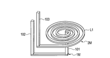
- the second conductor layer 2M is a first inductor layer in which a first inductor L1 having a spiral conductive pattern as shown in FIG. 3 is formed. One end of the first inductor L1 located at the center of the conductive pattern is electrically connected to the first conductor layer 1M by the plug 101 formed in the insulating layer 135.
- the “plug” has a structure in which a conductive material is embedded in a through hole formed in the insulating layer 135.
- the first conductor layer 1M is electrically connected to the pad P1a disposed on the upper surface of the chip transformer 100 via the plug 102. That is, the first conductor layer 1M is used as part of the wiring that electrically connects the first inductor L1 and the pad P1a. On the other hand, the other end located at the outer edge of the first inductor L1 is electrically connected to the pad P1b disposed on the upper surface of the chip transformer 100 via the plug 103.
- the fourth conductor layer 4M is exposed on the surface of the stacked body 130 and disposed on the upper surface of the chip transformer 100.
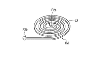
- the fourth conductor layer 4M is a second inductor layer in which a second inductor L2 having a spiral conductive pattern as shown in FIG. 4 is formed.
- One end of the second inductor L2 located at the center of the conductive pattern is electrically connected to the pad P2a disposed on the inner side of the conductive pattern on the upper surface of the chip transformer 100.
- the other end located at the outer edge of the second inductor L2 is electrically connected to a pad P2b disposed outside the conductive pattern on the upper surface of the chip transformer 100.
- the chip transformer 100 signal propagation by magnetic field coupling is performed between the pads P1a and P1b and the pads P2a and P2b by the above structure in which the first inductor layer and the second inductor layer are stacked via the insulating layer. Is called. It is preferable to form the first inductor L1 and the second inductor L2 so that the respective center positions coincide in plan view. According to the chip transformer 100, high-speed pulse signal communication having a pulse width of about several nanoseconds is possible.
- the thickness of the second conductor layer 2M is set to about 1 ⁇ m
- the thickness of the fourth conductor layer 4M is set to about 4 ⁇ m.
- the on-resistance on the transmission side is smaller than that on the reception side in order to stably perform high-frequency signal propagation.
- the pad P2a and the pad P2b connected to the second inductor L2 formed in the fourth conductor layer 4M having a large thickness are used as the transmission side terminal Tx.
- the pads P1a and P1b connected to the first inductor L1 formed on the second conductor layer 2M having a small film thickness are used as the reception-side terminal Rx. This facilitates the manufacture of the chip transformer 100 with good flatness.
- the film thickness of the second conductor layer 2M may be set to the same thickness as the film thickness of the fourth conductor layer 4M. Or you may make the film thickness of the 2nd conductor layer 2M thicker than the film thickness of the 4th conductor layer 4M.
- the pad P1a and the pad P1b connected to the first inductor L1 formed in the second conductor layer 2M can be used as the transmission side terminal Tx. Then, the pad P2a and the pad P2b connected to the second inductor L2 formed in the fourth conductor layer 4M are set as the reception side terminal Rx.
- a conductive shield 136 as shown in FIG. 5 between the first inductor L1 and the second inductor L2.
- the shield 136 is formed on the third conductor layer 3M. This is due to the following reasons.
- a parasitic capacitance is formed between the first inductor L1 and the second inductor L2.
- the charges accumulated in the parasitic capacitance move to an external circuit and an abnormal voltage or current is generated.
- the shield 136 By arranging the shield 136 between the first inductor L1 and the second inductor L2, the charge of the parasitic capacitance is discharged through the shield 136. Thereby, it can suppress that noise generate
- the shield 136 is formed so as not to disturb the magnetic field communication in the chip transformer 100.
- a U-shaped plate-shaped conductor shield 136 as shown in FIG. 5 is used so that the shield 136 does not shield between the centers of the first inductor L1 and the second inductor L2.
- the shield 136 is electrically connected to the pad Ps disposed on the upper surface of the chip transformer 100 via the plug 106.
- the pad Ps is grounded, for example, via a semiconductor chip to which the receiving side terminal Rx is connected.
- Examples of the material of the first conductor layer 1M, the second conductor layer 2M, the third conductor layer 3M, and the fourth conductor layer 4M include aluminum (Al), copper (Cu), and AlCu. Conductive materials can be used. In addition, the conductive material can be used for the plugs 101 to 106 embedded in the insulating layer 135.
- FIG. 6 shows a configuration example in which the semiconductor device 10 includes the first semiconductor chip 11, the second semiconductor chip 12, the transmission transformer 13, and the reception transformer 14.
- the receiving transformer 14 may not be included in the semiconductor device 10.
- the semiconductor device 10 may include another semiconductor chip.
- a semiconductor chip that steps down a high voltage supplied from the outside to a power supply voltage suitable for the first semiconductor chip 11 may be incorporated in the semiconductor device 10.
- the operation of the external element 30 is controlled by the serial transmission / reception function.
- the serial transmission / reception function an on signal for turning on the external element 30 and an off signal for turning off the external element 30 are sequentially output.
- the external element 30 is surely in the off state until the on signal drive signal Sd is input. Therefore, according to the control by the semiconductor device 10, it is possible to prevent a malfunction caused by erroneously overlapping ON signal inputs, which is caused by the control by the parallel transmission / reception function.
- the semiconductor device 10 used as a part of the in-vehicle electronic circuit system drives an electric motor, it is possible to prevent an accident in which a large through current flows because two transistors connected in series are simultaneously turned on.
- the channel through which the control signal Sc propagates from the first semiconductor chip 11 to the second semiconductor chip 12 is an insulating structure using the transmission transformer 13. It is.
- the channel through which the return signal Sr propagates from the second semiconductor chip 12 to the first semiconductor chip 11 has an insulating structure using the reception transformer 14. That is, signal propagation between the first semiconductor chip 11 and the second semiconductor chip in an electrically insulated state is performed via the chip transformer 100. Since the chip transformer 100 is small in size, according to the semiconductor device 10, it is possible to propagate a stable signal at a high speed while suppressing the influence of an external magnetic field.
- the light receiving characteristic of the light receiving element is deteriorated due to deterioration of the luminance of the light emitting element such as a light emitting diode, and the signal propagation responsiveness is lowered.
- the optical device is placed in a high temperature environment, the luminance of the light emitting element is deteriorated and the light receiving characteristics of the light receiving element are rapidly deteriorated, and the service life is shortened.
- the semiconductor device 10 according to the embodiment of the present invention a transformer is used instead of an optical device for the signal propagation path, so that the signal propagation responsiveness is not lowered and the service life is not shortened.
- the semiconductor device 10 according to the embodiment is suitable for in-vehicle use in which the environmental temperature is high.
- the use of a chip transformer improves the signal propagation speed and operational stability compared to the case of using a substrate transformer.
- the semiconductor device of the present invention can be used for a semiconductor device in which a plurality of semiconductor chips are arranged so as to be insulated from each other.
Landscapes
- Engineering & Computer Science (AREA)
- Power Engineering (AREA)
- Computer Networks & Wireless Communication (AREA)
- Signal Processing (AREA)
- Microelectronics & Electronic Packaging (AREA)
- Semiconductor Integrated Circuits (AREA)
Abstract
第1の半導体チップと、第1の半導体チップと電気的に絶縁して配置された第2の半導体チップと、導電体層と絶縁層が積層されたチップトランスであって、送信側端子が第1の半導体チップに接続し、受信側端子が第2の半導体チップに接続する送信トランスとを備え、送信トランスを介して第1の半導体チップから第2の半導体チップに第2の半導体チップの動作を制御する制御信号が送信される。
Description
本発明は、互いに絶縁分離された複数の半導体チップを有する半導体装置に関する。
例えば高い電源電圧で駆動される高電圧系の半導体チップと、この半導体チップの動作を制御する電源電圧の低い半導体チップとを1つの半導体装置として一体化することにより、部品数の低減や省スペース化を実現できる。この場合、高電圧系の半導体チップによる感電事故などを防止するために、半導体チップ間を電気的に絶縁分離することが好ましい。絶縁分離された半導体チップ間の信号伝播に、オプティカルデバイスやトランスを使用することが有効であると考えられる。例えば、基板トランスを用いることによって信号の伝播速度を高速化する方法が提案されている(例えば、特許文献1参照。)。
しかしながら、信号伝播にトランスを使用する技術については、十分な検討がなされていない。本発明は、絶縁分離された半導体チップ間の信号伝播速度が向上された半導体装置を提供することを目的とする。
本発明の一態様によれば、(ア)第1の半導体チップと、(イ)第1の半導体チップと電気的に絶縁して配置された第2の半導体チップと、(ウ)導電体層と絶縁層が積層されたチップトランスであって、送信側端子が第1の半導体チップに接続し、受信側端子が第2の半導体チップに接続する送信トランスとを備え、送信トランスを介して第1の半導体チップから第2の半導体チップに第2の半導体チップの動作を制御する制御信号が送信される半導体装置が提供される。
本発明によれば、絶縁分離された半導体チップ間の信号伝播速度が向上された半導体装置を提供できる。
次に、図面を参照して、本発明の実施形態を説明する。以下の図面の記載において、同一又は類似の部分には同一又は類似の符号を付している。ただし、図面は模式的なものであり、厚みと平面寸法との関係、各部の長さの比率等は現実のものとは異なることに留意すべきである。したがって、具体的な寸法は以下の説明を参酌して判断すべきものである。また、図面相互間においても互いの寸法の関係や比率が異なる部分が含まれていることはもちろんである。
また、以下に示す実施形態は、この発明の技術的思想を具体化するための装置や方法を例示するものであって、この発明の技術的思想は、構成部品の形状、構造、配置等を下記のものに特定するものでない。この発明の実施形態は、請求の範囲において、種々の変更を加えることができる。
本発明の実施形態に係る半導体装置10は、図1に示すように、第1の半導体チップ11、第2の半導体チップ12、送信トランス13及び受信トランス14を備える。第1の半導体チップ11、第2の半導体チップ12、送信トランス13、及び受信トランス14は、絶縁性樹脂などのモールド材15によってモールド封止され、一体化されている。第1の半導体チップ11と第2の半導体チップ12とは電気的に絶縁して配置されている。送信トランス13及び受信トランス14は、導電体層と絶縁層が積層されたチップトランスである。チップトランスの構造の詳細については後述する。
第1の半導体チップ11は、第2の半導体チップ12の動作を制御する制御信号Scを出力する。制御信号Scは、送信トランス13を介して、第1の半導体チップ11から第2の半導体チップ12に送信される。即ち、送信トランス13は、送信側端子Txが第1の半導体チップ11に接続し、受信側端子Rxが第2の半導体チップ12に接続する。ここで、チップトランスを伝播する信号が外部から入力する端子を「送信側端子」、外部に信号が出力される端子を「受信側端子」という。第1の半導体チップ11の動作は、マイクロプロセッサ20から第1の半導体チップ11に送信される信号Saによって制御される。一方、第1の半導体チップ11からマイクロプロセッサ20に、信号Sbが送信される。信号Sbは、外部素子30、第2の半導体チップ12及び第1の半導体チップ11それぞれの状態を確認するための信号である。
受信トランス14を介して、制御信号Scに対応した第2の半導体チップ12からの戻り信号Srが第1の半導体チップ11に送信される。このため、受信トランス14の送信側端子Txは第2の半導体チップ12に接続し、受信側端子Rxは第1の半導体チップ11に接続する。戻り信号Srは、制御信号Scを受信した第2の半導体チップ12の動作に応じて値が定まるように発生される。戻り信号Srによって、第2の半導体チップ12が正常に動作しているか否かなどを第1の半導体チップ11が判定可能である。
第2の半導体チップ12には、外部素子30を駆動する駆動回路が形成されている。そして、第2の半導体チップ12から、外部素子30を駆動する駆動信号Sdが外部素子30に出力される。一方、外部素子30から第2の半導体チップ12に戻り信号Smが出力される。戻り信号Smは、外部素子30の状態を確認するための信号である。
外部素子30は、例えば絶縁ゲートバイポーラトランジスタ(IGBT)などである。第1の半導体チップ11及び第2の半導体チップ12には、それぞれの半導体チップに電力を供給する個別の電源回路(図示略)が用意されている。
例えば10A程度の出力電流を実現するために、第2の半導体チップ12の駆動能力は高く設定される。これにより、第2の半導体チップ12が駆動する外部素子30として最大定格の大きなIGBTを使用した場合にも、外部素子30の高速のオン・オフ動作が可能である。第2の半導体チップ12に要求される駆動能力に応じて、第2の半導体チップ12に電力を供給する電源回路の仕様が設定される。
半導体装置10は、例えばハイブリッド車の車載電子回路システムの一部として使用することができる。例えば、第2の半導体チップ12をハイブリッド車の高電圧系回路を駆動する駆動装置として使用する。ここで、高電圧系回路は電気モータを駆動する回路などである。電気モータを駆動するためには、例えば200V系バッテリーの出力を500V~900Vの高電圧に昇圧する。第1の半導体チップ11をハイブリッド車の低電圧系回路を駆動する駆動装置として使用する。ここで、低電圧系回路は、車載電子回路、ヘッドライトやウィンカーなどの灯光類、ガソリンエンジンやディーゼルエンジンなどの内燃機関の発火装置などの、12V系若しくは24V系バッテリーによって電源が供給される回路である。
第2の半導体チップ12の動作を制御する第1の半導体チップ11には、第2の半導体チップ12のような高い駆動能力は必要ない。したがって、第1の半導体チップ11の内部電圧は、例えば数V程度に設定される。
既に述べたように、半導体装置10においては、第1の半導体チップ11と第2の半導体チップ12とは電気的に絶縁して配置されている。そして、制御信号Scが第1の半導体チップ11から第2の半導体チップ12に伝播するチャンネルは、送信トランス13を用いた絶縁構造である。また、戻り信号Srが第2の半導体チップ12から第1の半導体チップ11に伝播するチャンネルは、受信トランス14を用いた絶縁構造である。送信トランス13及び受信トランス14は、パルス信号が伝播可能なパルストランスである。このように、第1の半導体チップ11と第2の半導体チップ12とは電気的に絶縁されている。これにより、例えば第1の半導体チップ11に人体が接触しても、高電圧が供給される第2の半導体チップ12による感電事故などを抑制できる。
なお、送信トランス13に基板トランスを使用することも可能である。しかし、チップトランスは基板トランスよりもサイズが小さく、結合容量が小さい。このため、チップトランスを使用することにより、信号の伝播速度を向上できる。また、チップトランスを使用することによって、半導体装置10全体のサイズを小さくすることができる。更に、送信トランス13や受信トランス14のサイズが小さいことにより、半導体装置10が受ける外部磁界の影響を抑制することができる。例えば素子電流の大きな外部素子が送信トランス13の周囲に配置された場合などに、外部素子の動作に起因して発生する磁界によって半導体装置10が受ける影響を抑制できる。
次に、送信トランス13や受信トランス14に使用可能なチップトランスの構造例について説明する。送信トランス13や受信トランス14には、例えば図2に示すような構造を採用可能である。
図2に示すチップトランス100は、複数の導電体層が絶縁層を挟んで積層された積層構造である。例えばシリコン基板などの半導体基板110上に、酸化シリコン膜などの絶縁膜120を介して、複数の導電体層を含む積層体130が配置されている。積層体130は、第1の導電体層1M、第2の導電体層2M、第3の導電体層3M、及び第4の導電体層4Mが、絶縁層135を介して積層された構造である。例えば、半導体基板110の膜厚は400μm程度、積層体130の膜厚は10~30μm程度である。
第2の導電体層2Mは、図3に示すような渦巻き状の導電性パターンを有する第1のインダクタL1が形成された第1のインダクタ層である。導電性パターンの中心部に位置する第1のインダクタL1の一方の端部が、絶縁層135に形成されたプラグ101によって第1の導電体層1Mと電気的に接続する。「プラグ」は、絶縁層135に形成されたスルーホールに導電性材料を埋め込んだ構造である。
第1の導電体層1Mは、プラグ102を介して、チップトランス100の上面に配置されたパッドP1aと電気的に接続されている。つまり、第1の導電体層1Mは、第1のインダクタL1とパッドP1aとを電気的に接続する配線の一部として使用される。一方、第1のインダクタL1の外縁部に位置する他方の端部は、プラグ103を介して、チップトランス100の上面に配置されたパッドP1bと電気的に接続されている。
第4の導電体層4Mは、積層体130表面に露出してチップトランス100の上面に配置されている。第4の導電体層4Mは、図4に示すような渦巻き状の導電性パターンを有する第2のインダクタL2が形成された第2のインダクタ層である。導電性パターンの中心部に位置する第2のインダクタL2の一方の端部が、チップトランス100の上面で導電性パターンの内側に配置されたパッドP2aと電気的に接続されている。第2のインダクタL2の外縁部に位置する他方の端部は、チップトランス100の上面で導電性パターンの外側に配置されたパッドP2bと電気的に接続されている。
チップトランス100では、第1のインダクタ層と第2のインダクタ層とが絶縁層を介して積層された上記構造によって、パッドP1a、P1bとパッドP2a、P2bとの間で磁界結合による信号伝播が行われる。それぞれの中心位置が平面視で一致するように、第1のインダクタL1と第2のインダクタL2とを形成することが好ましい。チップトランス100によれば、パルス幅が数ナノ秒程度の高速なパルス信号通信が可能である。
ところで、積層体130の下層側である第2の導電体層2Mの膜厚を厚くすると、平坦性が悪くなり、第2の導電体層2M以降の工程で不良が生じるなどの問題が起こる。このため、第4の導電体層4Mの膜厚を厚くすることは比較的容易であるが、第2の導電体層2Mの膜厚を厚くすることは難しい。例えば、第2の導電体層2Mの膜厚を1μm程度、第4の導電体層4Mの膜厚を4μm程度に設定する。
チップトランス100を用いて磁界結合による信号伝播を行う場合、安定して高周波の信号伝播を行うためには受信側よりも送信側のオン抵抗が小さいことが好ましい。このため、膜厚が厚い第4の導電体層4Mに形成された第2のインダクタL2に接続するパッドP2a及びパッドP2bを送信側端子Txとする。そして、膜厚が薄い第2の導電体層2Mに形成された第1のインダクタL1に接続するパッドP1a及びパッドP1bを受信側端子Rxとする。これにより、平坦性の良いチップトランス100の製造が容易になる。
なお、平坦性が確保できる場合や平坦性が問題にならない場合には、第2の導電体層2Mの膜厚を第4の導電体層4Mの膜厚と同程度にしてもよい。或いは第2の導電体層2Mの膜厚を第4の導電体層4Mの膜厚よりも厚くしてもよい。その場合、第2の導電体層2Mに形成される第1のインダクタL1に接続するパッドP1a及びパッドP1bを、送信側端子Txとすることができる。そして、第4の導電体層4Mに形成される第2のインダクタL2に接続するパッドP2a及びパッドP2bを、受信側端子Rxとする。
チップトランス100では、第1のインダクタL1と第2のインダクタL2との間に、図5に示すような導電性のシールド136を配置することが好ましい。シールド136は、第3の導電体層3Mに形成される。これは、以下のような理由による。
チップトランス100では、第1のインダクタL1と第2のインダクタL2の間に寄生容量が形成される。寄生容量に蓄積された電荷が外部回路に移動して、異常な電圧や電流が発生するおそれがある。第1のインダクタL1と第2のインダクタL2の間にシールド136を配置することによって、寄生容量の電荷がシールド136を介して放出される。これにより、半導体装置10の出力にノイズが発生することを抑制できる。
シールド136は、チップトランス100での磁界通信を妨害しないように形成される。例えば図5に示すようなU字形状の板状導電体のシールド136を使用し、第1のインダクタL1と第2のインダクタL2の中心間をシールド136によって遮蔽しないようする。
シールド136は、プラグ106を介してチップトランス100の上面に配置されたパッドPsと電気的に接続される。パッドPsは、例えば受信側端子Rxが接続される半導体チップを介して接地される。
第1の導電体層1M、第2の導電体層2M、第3の導電体層3M及び第4の導電体層4Mの材料には、例えばアルミニウム(Al)、銅(Cu)、AlCuなどの導電性材料を使用可能である。また、絶縁層135に埋め込まれるプラグ101~プラグ106にも上記の導電性材料を使用可能である。
なお、図6では半導体装置10が第1の半導体チップ11、第2の半導体チップ12、送信トランス13及び受信トランス14を備える構成例を示した。しかし、受信トランス14が半導体装置10に含まれなくてもよい。また、半導体装置10が他の半導体チップを備えていてもよい。例えば、外部から供給される高電圧を第1の半導体チップ11に適応した電源電圧に降圧する半導体チップなどを、半導体装置10に内蔵させてもよい。
また、信号伝播が1チャンネルで行われる半導体装置10では、シリアル送受信機能によって外部素子30の動作が制御される。シリアル送受信機能では、外部素子30をオン状態にするオン信号と外部素子30をオフ状態にするオフ信号を順番に出力する。このシリアル送受信機能を採用することにより、オン信号の駆動信号Sdが入力されるまで外部素子30は確実にオフ状態である。したがって、半導体装置10による制御によれば、パラレル送受信機能による制御で生じるような、誤ってオン信号の入力が重なることによる誤動作などを防止できる。例えば、車載電子回路システムの一部として使用された半導体装置10が電気モータを駆動する場合などに、直列接続された2つのトランジスタが同時にオン状態になって大きな貫通電流が流れる事故を防止できる。
以上に説明したように、本発明の実施形態に係る半導体装置10では、制御信号Scが第1の半導体チップ11から第2の半導体チップ12に伝播するチャンネルは、送信トランス13を用いた絶縁構造である。また、戻り信号Srが第2の半導体チップ12から第1の半導体チップ11に伝播するチャンネルは、受信トランス14を用いた絶縁構造である。つまり、電気的に絶縁した状態の第1の半導体チップ11と第2の半導体チップとの間の信号伝播が、チップトランス100を介して行われる。チップトランス100はサイズが小さいため、半導体装置10によれば、高速且つ外部からの磁界の影響が抑制された安定した信号の伝播が可能である。
本発明の実施形態と異なり、信号伝播経路にオプティカルデバイスを使用した場合には、発光ダイオードなどの発光素子の輝度が劣化することにより受光素子の受光特性が低下し、信号伝播応答性が低くなる。更に、オプティカルデバイスが高温環境下に置かれると発光素子の輝度の劣化や受光素子の受光特性の低下が速くなり、耐用年数が短くなる。
これに対し、本発明の実施形態に係る半導体装置10では、信号伝播経路にオプティカルデバイスではなくトランスを使用するため、信号の伝播応答性が低下することなく、且つ耐用年数が短くなることもない。例えば、環境温度が高温になる車載用としても、実施形態に係る半導体装置10は好適である。また、チップトランスを使用することにより、基板トランスを使用する場合に比べて信号の伝播速度や動作の安定性が向上する。
(その他の実施形態)
上記のように、本発明は実施形態によって記載したが、この開示の一部をなす論述及び図面はこの発明を限定するものであると理解すべきではない。この開示から当業者には様々な代替実施形態、実施例及び運用技術が明らかとなろう。即ち、本発明はここでは記載していない様々な実施形態等を含むことは勿論である。したがって、本発明の技術的範囲は上記の説明から妥当な請求の範囲に係る発明特定事項によってのみ定められるものである。
上記のように、本発明は実施形態によって記載したが、この開示の一部をなす論述及び図面はこの発明を限定するものであると理解すべきではない。この開示から当業者には様々な代替実施形態、実施例及び運用技術が明らかとなろう。即ち、本発明はここでは記載していない様々な実施形態等を含むことは勿論である。したがって、本発明の技術的範囲は上記の説明から妥当な請求の範囲に係る発明特定事項によってのみ定められるものである。
本発明の半導体装置は、複数の半導体チップが互いに絶縁分離されて配置された半導体装置の用途に利用可能である。
Claims (7)
- 第1の半導体チップと、
前記第1の半導体チップと電気的に絶縁して配置された第2の半導体チップと、
導電体層と絶縁層が積層されたチップトランスであって、送信側端子が前記第1の半導体チップに接続し、受信側端子が前記第2の半導体チップに接続する送信トランスと
を備え、前記送信トランスを介して前記第1の半導体チップから前記第2の半導体チップに前記第2の半導体チップの動作を制御する制御信号が送信されることを特徴とする半導体装置。 - 前記送信トランスが、
渦巻き状の導電性パターンを有する第1のインダクタが形成された第1のインダクタ層と、
渦巻き状の導電性パターンを有する第2のインダクタが形成された第2のインダクタ層と、
前記第1のインダクタ層と前記第2のインダクタ層との間に配置された絶縁層と
を備えるチップトランスであることを特徴とする請求項1に記載の半導体装置。 - 前記第1のインダクタ層の上方に配置される前記第2のインダクタ層の膜厚が前記第1のインダクタ層の膜厚よりも厚く、
前記第1のインダクタが前記受信側端子に接続し、
前記第2のインダクタが前記送信側端子に接続する
ことを特徴とする請求項2に記載の半導体装置。 - 前記第1のインダクタと前記第2のインダクタとの間で前記絶縁層の内部に配置された導電性のシールドを更に備えることを特徴とする請求項2に記載の半導体装置。
- 前記第1の半導体チップ、前記第2の半導体チップ及び前記送信トランスが、モールド封止によって一体化されていることを特徴とする請求項1に記載の半導体装置。
- 導電体層と絶縁層が積層されたチップトランスであって、送信側端子が前記第2の半導体チップに接続し、受信側端子が前記第1の半導体チップに接続する受信トランスを更に備え、
前記受信トランスを介して、前記制御信号に対応した戻り信号が前記第2の半導体チップから前記第1の半導体チップに送信されることを特徴とする請求項1に記載の半導体装置。 - 前記第2の半導体チップによって駆動される外部素子をオン状態にするオン信号と前記外部素子をオフ状態にするオフ信号を順番に出力するシリアル送受信機能を備えることを特徴とする請求項1に記載の半導体装置。
Priority Applications (1)
| Application Number | Priority Date | Filing Date | Title |
|---|---|---|---|
| PCT/JP2015/070834 WO2017013768A1 (ja) | 2015-07-22 | 2015-07-22 | 半導体装置 |
Applications Claiming Priority (1)
| Application Number | Priority Date | Filing Date | Title |
|---|---|---|---|
| PCT/JP2015/070834 WO2017013768A1 (ja) | 2015-07-22 | 2015-07-22 | 半導体装置 |
Publications (1)
| Publication Number | Publication Date |
|---|---|
| WO2017013768A1 true WO2017013768A1 (ja) | 2017-01-26 |
Family
ID=57835173
Family Applications (1)
| Application Number | Title | Priority Date | Filing Date |
|---|---|---|---|
| PCT/JP2015/070834 Ceased WO2017013768A1 (ja) | 2015-07-22 | 2015-07-22 | 半導体装置 |
Country Status (1)
| Country | Link |
|---|---|
| WO (1) | WO2017013768A1 (ja) |
Cited By (2)
| Publication number | Priority date | Publication date | Assignee | Title |
|---|---|---|---|---|
| DE112018004476T5 (de) | 2017-10-09 | 2020-05-28 | Vernet | Thermostatische Kartusche zur Regelung zu vermischender kalter und heißer Fluide |
| JPWO2022210542A1 (ja) * | 2021-03-29 | 2022-10-06 |
Citations (4)
| Publication number | Priority date | Publication date | Assignee | Title |
|---|---|---|---|---|
| JPH04133408A (ja) * | 1990-09-26 | 1992-05-07 | Toshiba Lighting & Technol Corp | 平面トランス |
| JPH0766361A (ja) * | 1993-08-30 | 1995-03-10 | Hitachi Cable Ltd | 電源装置 |
| WO2013027454A1 (ja) * | 2011-08-25 | 2013-02-28 | サンケン電気株式会社 | 半導体装置 |
| JP2013229812A (ja) * | 2012-04-26 | 2013-11-07 | Renesas Electronics Corp | 送信回路及びそれを備えた半導体集積回路 |
-
2015
- 2015-07-22 WO PCT/JP2015/070834 patent/WO2017013768A1/ja not_active Ceased
Patent Citations (4)
| Publication number | Priority date | Publication date | Assignee | Title |
|---|---|---|---|---|
| JPH04133408A (ja) * | 1990-09-26 | 1992-05-07 | Toshiba Lighting & Technol Corp | 平面トランス |
| JPH0766361A (ja) * | 1993-08-30 | 1995-03-10 | Hitachi Cable Ltd | 電源装置 |
| WO2013027454A1 (ja) * | 2011-08-25 | 2013-02-28 | サンケン電気株式会社 | 半導体装置 |
| JP2013229812A (ja) * | 2012-04-26 | 2013-11-07 | Renesas Electronics Corp | 送信回路及びそれを備えた半導体集積回路 |
Cited By (4)
| Publication number | Priority date | Publication date | Assignee | Title |
|---|---|---|---|---|
| DE112018004476T5 (de) | 2017-10-09 | 2020-05-28 | Vernet | Thermostatische Kartusche zur Regelung zu vermischender kalter und heißer Fluide |
| JPWO2022210542A1 (ja) * | 2021-03-29 | 2022-10-06 | ||
| WO2022210542A1 (ja) * | 2021-03-29 | 2022-10-06 | ローム株式会社 | 絶縁トランス、絶縁モジュールおよびゲートドライバ |
| US12549180B2 (en) | 2021-03-29 | 2026-02-10 | Rohm Co., Ltd. | Isolation transformer, isolation module, and gate driver |
Similar Documents
| Publication | Publication Date | Title |
|---|---|---|
| US7834575B2 (en) | Gate-driver IC with HV-isolation, especially hybrid electric vehicle motor drive concept | |
| US20090184760A1 (en) | Driver IC with HV-isolation, especially hybrid electric vehicle motor drive concept | |
| CN105470243B (zh) | 半导体装置 | |
| US8487407B2 (en) | Low impedance gate control method and apparatus | |
| KR101123827B1 (ko) | 반도체 장치 | |
| US11227845B2 (en) | Power module and method of manufacturing same | |
| CN106898607A (zh) | 半导体器件 | |
| US20070158859A1 (en) | Power semiconductor module | |
| CN106797171A (zh) | 电力转换装置的控制基板 | |
| JP2015225918A (ja) | 半導体モジュールおよび半導体スイッチ | |
| WO2017013768A1 (ja) | 半導体装置 | |
| US9324788B2 (en) | Semiconductor device | |
| EP3288358B1 (en) | Electronic inverter assembly | |
| KR101294002B1 (ko) | 전기 자동차용 플러그 타입의 고전압 무접점 릴레이 | |
| ES2943137T3 (es) | Circuito de alta corriente | |
| EP2957762B1 (en) | Control apparatus | |
| JP5604083B2 (ja) | 制御機能を有し、トランスミッタを組み込んでいるパワー半導体モジュール | |
| JP5782919B2 (ja) | 半導体装置 | |
| KR20020021127A (ko) | 저인덕턴스 반도체 소자 | |
| WO2017013769A1 (ja) | 半導体装置 | |
| JP2020010435A (ja) | 電力変換装置 | |
| CN104126276A (zh) | 高频开关模块 | |
| US20140284617A1 (en) | Semiconductor device | |
| US12494782B2 (en) | Signal transmission device, electronic device, and vehicle | |
| US20250364895A1 (en) | Driver, signal transmission device, electronic device, and vehicle |
Legal Events
| Date | Code | Title | Description |
|---|---|---|---|
| 121 | Ep: the epo has been informed by wipo that ep was designated in this application |
Ref document number: 15898927 Country of ref document: EP Kind code of ref document: A1 |
|
| NENP | Non-entry into the national phase |
Ref country code: DE |
|
| NENP | Non-entry into the national phase |
Ref country code: JP |
|
| 122 | Ep: pct application non-entry in european phase |
Ref document number: 15898927 Country of ref document: EP Kind code of ref document: A1 |