WO2017006801A1 - キャリア基板、積層体、電子デバイスの製造方法 - Google Patents
キャリア基板、積層体、電子デバイスの製造方法 Download PDFInfo
- Publication number
- WO2017006801A1 WO2017006801A1 PCT/JP2016/069080 JP2016069080W WO2017006801A1 WO 2017006801 A1 WO2017006801 A1 WO 2017006801A1 JP 2016069080 W JP2016069080 W JP 2016069080W WO 2017006801 A1 WO2017006801 A1 WO 2017006801A1
- Authority
- WO
- WIPO (PCT)
- Prior art keywords
- substrate
- electronic device
- glass
- glass substrate
- laminate
- Prior art date
- Legal status (The legal status is an assumption and is not a legal conclusion. Google has not performed a legal analysis and makes no representation as to the accuracy of the status listed.)
- Ceased
Links
Images



Classifications
-
- H—ELECTRICITY
- H10—SEMICONDUCTOR DEVICES; ELECTRIC SOLID-STATE DEVICES NOT OTHERWISE PROVIDED FOR
- H10D—INORGANIC ELECTRIC SEMICONDUCTOR DEVICES
- H10D86/00—Integrated devices formed in or on insulating or conducting substrates, e.g. formed in silicon-on-insulator [SOI] substrates or on stainless steel or glass substrates
- H10D86/01—Manufacture or treatment
- H10D86/021—Manufacture or treatment of multiple TFTs
- H10D86/0214—Manufacture or treatment of multiple TFTs using temporary substrates
-
- B—PERFORMING OPERATIONS; TRANSPORTING
- B32—LAYERED PRODUCTS
- B32B—LAYERED PRODUCTS, i.e. PRODUCTS BUILT-UP OF STRATA OF FLAT OR NON-FLAT, e.g. CELLULAR OR HONEYCOMB, FORM
- B32B7/00—Layered products characterised by the relation between layers; Layered products characterised by the relative orientation of features between layers, or by the relative values of a measurable parameter between layers, i.e. products comprising layers having different physical, chemical or physicochemical properties; Layered products characterised by the interconnection of layers
- B32B7/02—Physical, chemical or physicochemical properties
-
- B—PERFORMING OPERATIONS; TRANSPORTING
- B32—LAYERED PRODUCTS
- B32B—LAYERED PRODUCTS, i.e. PRODUCTS BUILT-UP OF STRATA OF FLAT OR NON-FLAT, e.g. CELLULAR OR HONEYCOMB, FORM
- B32B17/00—Layered products essentially comprising sheet glass, or glass, slag, or like fibres
-
- B—PERFORMING OPERATIONS; TRANSPORTING
- B32—LAYERED PRODUCTS
- B32B—LAYERED PRODUCTS, i.e. PRODUCTS BUILT-UP OF STRATA OF FLAT OR NON-FLAT, e.g. CELLULAR OR HONEYCOMB, FORM
- B32B17/00—Layered products essentially comprising sheet glass, or glass, slag, or like fibres
- B32B17/06—Layered products essentially comprising sheet glass, or glass, slag, or like fibres comprising glass as the main or only constituent of a layer, next to another layer of a specific material
-
- B—PERFORMING OPERATIONS; TRANSPORTING
- B32—LAYERED PRODUCTS
- B32B—LAYERED PRODUCTS, i.e. PRODUCTS BUILT-UP OF STRATA OF FLAT OR NON-FLAT, e.g. CELLULAR OR HONEYCOMB, FORM
- B32B17/00—Layered products essentially comprising sheet glass, or glass, slag, or like fibres
- B32B17/06—Layered products essentially comprising sheet glass, or glass, slag, or like fibres comprising glass as the main or only constituent of a layer, next to another layer of a specific material
- B32B17/10—Layered products essentially comprising sheet glass, or glass, slag, or like fibres comprising glass as the main or only constituent of a layer, next to another layer of a specific material of synthetic resin
-
- B—PERFORMING OPERATIONS; TRANSPORTING
- B32—LAYERED PRODUCTS
- B32B—LAYERED PRODUCTS, i.e. PRODUCTS BUILT-UP OF STRATA OF FLAT OR NON-FLAT, e.g. CELLULAR OR HONEYCOMB, FORM
- B32B27/00—Layered products comprising a layer of synthetic resin
- B32B27/28—Layered products comprising a layer of synthetic resin comprising synthetic resins not wholly covered by any one of the sub-groups B32B27/30 - B32B27/42
- B32B27/281—Layered products comprising a layer of synthetic resin comprising synthetic resins not wholly covered by any one of the sub-groups B32B27/30 - B32B27/42 comprising polyimides
-
- B—PERFORMING OPERATIONS; TRANSPORTING
- B32—LAYERED PRODUCTS
- B32B—LAYERED PRODUCTS, i.e. PRODUCTS BUILT-UP OF STRATA OF FLAT OR NON-FLAT, e.g. CELLULAR OR HONEYCOMB, FORM
- B32B38/00—Ancillary operations in connection with laminating processes
- B32B38/10—Removing layers, or parts of layers, mechanically or chemically
-
- B—PERFORMING OPERATIONS; TRANSPORTING
- B32—LAYERED PRODUCTS
- B32B—LAYERED PRODUCTS, i.e. PRODUCTS BUILT-UP OF STRATA OF FLAT OR NON-FLAT, e.g. CELLULAR OR HONEYCOMB, FORM
- B32B43/00—Operations specially adapted for layered products and not otherwise provided for, e.g. repairing; Apparatus therefor
- B32B43/006—Delaminating
-
- B—PERFORMING OPERATIONS; TRANSPORTING
- B32—LAYERED PRODUCTS
- B32B—LAYERED PRODUCTS, i.e. PRODUCTS BUILT-UP OF STRATA OF FLAT OR NON-FLAT, e.g. CELLULAR OR HONEYCOMB, FORM
- B32B7/00—Layered products characterised by the relation between layers; Layered products characterised by the relative orientation of features between layers, or by the relative values of a measurable parameter between layers, i.e. products comprising layers having different physical, chemical or physicochemical properties; Layered products characterised by the interconnection of layers
- B32B7/04—Interconnection of layers
- B32B7/06—Interconnection of layers permitting easy separation
-
- B—PERFORMING OPERATIONS; TRANSPORTING
- B32—LAYERED PRODUCTS
- B32B—LAYERED PRODUCTS, i.e. PRODUCTS BUILT-UP OF STRATA OF FLAT OR NON-FLAT, e.g. CELLULAR OR HONEYCOMB, FORM
- B32B7/00—Layered products characterised by the relation between layers; Layered products characterised by the relative orientation of features between layers, or by the relative values of a measurable parameter between layers, i.e. products comprising layers having different physical, chemical or physicochemical properties; Layered products characterised by the interconnection of layers
- B32B7/04—Interconnection of layers
- B32B7/12—Interconnection of layers using interposed adhesives or interposed materials with bonding properties
-
- B—PERFORMING OPERATIONS; TRANSPORTING
- B32—LAYERED PRODUCTS
- B32B—LAYERED PRODUCTS, i.e. PRODUCTS BUILT-UP OF STRATA OF FLAT OR NON-FLAT, e.g. CELLULAR OR HONEYCOMB, FORM
- B32B9/00—Layered products comprising a layer of a particular substance not covered by groups B32B11/00 - B32B29/00
- B32B9/04—Layered products comprising a layer of a particular substance not covered by groups B32B11/00 - B32B29/00 comprising such particular substance as the main or only constituent of a layer, which is next to another layer of the same or of a different material
- B32B9/041—Layered products comprising a layer of a particular substance not covered by groups B32B11/00 - B32B29/00 comprising such particular substance as the main or only constituent of a layer, which is next to another layer of the same or of a different material of metal
-
- B—PERFORMING OPERATIONS; TRANSPORTING
- B32—LAYERED PRODUCTS
- B32B—LAYERED PRODUCTS, i.e. PRODUCTS BUILT-UP OF STRATA OF FLAT OR NON-FLAT, e.g. CELLULAR OR HONEYCOMB, FORM
- B32B9/00—Layered products comprising a layer of a particular substance not covered by groups B32B11/00 - B32B29/00
- B32B9/04—Layered products comprising a layer of a particular substance not covered by groups B32B11/00 - B32B29/00 comprising such particular substance as the main or only constituent of a layer, which is next to another layer of the same or of a different material
- B32B9/045—Layered products comprising a layer of a particular substance not covered by groups B32B11/00 - B32B29/00 comprising such particular substance as the main or only constituent of a layer, which is next to another layer of the same or of a different material of synthetic resin
-
- C—CHEMISTRY; METALLURGY
- C03—GLASS; MINERAL OR SLAG WOOL
- C03C—CHEMICAL COMPOSITION OF GLASSES, GLAZES OR VITREOUS ENAMELS; SURFACE TREATMENT OF GLASS; SURFACE TREATMENT OF FIBRES OR FILAMENTS MADE FROM GLASS, MINERALS OR SLAGS; JOINING GLASS TO GLASS OR OTHER MATERIALS
- C03C17/00—Surface treatment of glass, not in the form of fibres or filaments, by coating
- C03C17/22—Surface treatment of glass, not in the form of fibres or filaments, by coating with other inorganic material
-
- C—CHEMISTRY; METALLURGY
- C03—GLASS; MINERAL OR SLAG WOOL
- C03C—CHEMICAL COMPOSITION OF GLASSES, GLAZES OR VITREOUS ENAMELS; SURFACE TREATMENT OF GLASS; SURFACE TREATMENT OF FIBRES OR FILAMENTS MADE FROM GLASS, MINERALS OR SLAGS; JOINING GLASS TO GLASS OR OTHER MATERIALS
- C03C17/00—Surface treatment of glass, not in the form of fibres or filaments, by coating
- C03C17/22—Surface treatment of glass, not in the form of fibres or filaments, by coating with other inorganic material
- C03C17/225—Nitrides
-
- C—CHEMISTRY; METALLURGY
- C03—GLASS; MINERAL OR SLAG WOOL
- C03C—CHEMICAL COMPOSITION OF GLASSES, GLAZES OR VITREOUS ENAMELS; SURFACE TREATMENT OF GLASS; SURFACE TREATMENT OF FIBRES OR FILAMENTS MADE FROM GLASS, MINERALS OR SLAGS; JOINING GLASS TO GLASS OR OTHER MATERIALS
- C03C17/00—Surface treatment of glass, not in the form of fibres or filaments, by coating
- C03C17/22—Surface treatment of glass, not in the form of fibres or filaments, by coating with other inorganic material
- C03C17/23—Oxides
-
- C—CHEMISTRY; METALLURGY
- C03—GLASS; MINERAL OR SLAG WOOL
- C03C—CHEMICAL COMPOSITION OF GLASSES, GLAZES OR VITREOUS ENAMELS; SURFACE TREATMENT OF GLASS; SURFACE TREATMENT OF FIBRES OR FILAMENTS MADE FROM GLASS, MINERALS OR SLAGS; JOINING GLASS TO GLASS OR OTHER MATERIALS
- C03C17/00—Surface treatment of glass, not in the form of fibres or filaments, by coating
- C03C17/28—Surface treatment of glass, not in the form of fibres or filaments, by coating with organic material
- C03C17/30—Surface treatment of glass, not in the form of fibres or filaments, by coating with organic material with silicon-containing compounds
-
- C—CHEMISTRY; METALLURGY
- C03—GLASS; MINERAL OR SLAG WOOL
- C03C—CHEMICAL COMPOSITION OF GLASSES, GLAZES OR VITREOUS ENAMELS; SURFACE TREATMENT OF GLASS; SURFACE TREATMENT OF FIBRES OR FILAMENTS MADE FROM GLASS, MINERALS OR SLAGS; JOINING GLASS TO GLASS OR OTHER MATERIALS
- C03C17/00—Surface treatment of glass, not in the form of fibres or filaments, by coating
- C03C17/28—Surface treatment of glass, not in the form of fibres or filaments, by coating with organic material
- C03C17/32—Surface treatment of glass, not in the form of fibres or filaments, by coating with organic material with synthetic or natural resins
-
- C—CHEMISTRY; METALLURGY
- C03—GLASS; MINERAL OR SLAG WOOL
- C03C—CHEMICAL COMPOSITION OF GLASSES, GLAZES OR VITREOUS ENAMELS; SURFACE TREATMENT OF GLASS; SURFACE TREATMENT OF FIBRES OR FILAMENTS MADE FROM GLASS, MINERALS OR SLAGS; JOINING GLASS TO GLASS OR OTHER MATERIALS
- C03C27/00—Joining pieces of glass to pieces of other inorganic material; Joining glass to glass other than by fusing
- C03C27/06—Joining glass to glass by processes other than fusing
-
- C—CHEMISTRY; METALLURGY
- C03—GLASS; MINERAL OR SLAG WOOL
- C03C—CHEMICAL COMPOSITION OF GLASSES, GLAZES OR VITREOUS ENAMELS; SURFACE TREATMENT OF GLASS; SURFACE TREATMENT OF FIBRES OR FILAMENTS MADE FROM GLASS, MINERALS OR SLAGS; JOINING GLASS TO GLASS OR OTHER MATERIALS
- C03C27/00—Joining pieces of glass to pieces of other inorganic material; Joining glass to glass other than by fusing
- C03C27/06—Joining glass to glass by processes other than fusing
- C03C27/10—Joining glass to glass by processes other than fusing with the aid of adhesive specially adapted for that purpose
-
- C—CHEMISTRY; METALLURGY
- C03—GLASS; MINERAL OR SLAG WOOL
- C03C—CHEMICAL COMPOSITION OF GLASSES, GLAZES OR VITREOUS ENAMELS; SURFACE TREATMENT OF GLASS; SURFACE TREATMENT OF FIBRES OR FILAMENTS MADE FROM GLASS, MINERALS OR SLAGS; JOINING GLASS TO GLASS OR OTHER MATERIALS
- C03C3/00—Glass compositions
- C03C3/04—Glass compositions containing silica
- C03C3/076—Glass compositions containing silica with 40% to 90% silica, by weight
- C03C3/089—Glass compositions containing silica with 40% to 90% silica, by weight containing boron
- C03C3/091—Glass compositions containing silica with 40% to 90% silica, by weight containing boron containing aluminium
-
- H—ELECTRICITY
- H10—SEMICONDUCTOR DEVICES; ELECTRIC SOLID-STATE DEVICES NOT OTHERWISE PROVIDED FOR
- H10D—INORGANIC ELECTRIC SEMICONDUCTOR DEVICES
- H10D30/00—Field-effect transistors [FET]
- H10D30/60—Insulated-gate field-effect transistors [IGFET]
- H10D30/67—Thin-film transistors [TFT]
- H10D30/674—Thin-film transistors [TFT] characterised by the active materials
- H10D30/6741—Group IV materials, e.g. germanium or silicon carbide
- H10D30/6743—Silicon
- H10D30/6745—Polycrystalline or microcrystalline silicon
-
- H—ELECTRICITY
- H10—SEMICONDUCTOR DEVICES; ELECTRIC SOLID-STATE DEVICES NOT OTHERWISE PROVIDED FOR
- H10D—INORGANIC ELECTRIC SEMICONDUCTOR DEVICES
- H10D86/00—Integrated devices formed in or on insulating or conducting substrates, e.g. formed in silicon-on-insulator [SOI] substrates or on stainless steel or glass substrates
- H10D86/40—Integrated devices formed in or on insulating or conducting substrates, e.g. formed in silicon-on-insulator [SOI] substrates or on stainless steel or glass substrates characterised by multiple TFTs
- H10D86/421—Integrated devices formed in or on insulating or conducting substrates, e.g. formed in silicon-on-insulator [SOI] substrates or on stainless steel or glass substrates characterised by multiple TFTs having a particular composition, shape or crystalline structure of the active layer
-
- H—ELECTRICITY
- H10—SEMICONDUCTOR DEVICES; ELECTRIC SOLID-STATE DEVICES NOT OTHERWISE PROVIDED FOR
- H10D—INORGANIC ELECTRIC SEMICONDUCTOR DEVICES
- H10D86/00—Integrated devices formed in or on insulating or conducting substrates, e.g. formed in silicon-on-insulator [SOI] substrates or on stainless steel or glass substrates
- H10D86/40—Integrated devices formed in or on insulating or conducting substrates, e.g. formed in silicon-on-insulator [SOI] substrates or on stainless steel or glass substrates characterised by multiple TFTs
- H10D86/60—Integrated devices formed in or on insulating or conducting substrates, e.g. formed in silicon-on-insulator [SOI] substrates or on stainless steel or glass substrates characterised by multiple TFTs wherein the TFTs are in active matrices
-
- H—ELECTRICITY
- H10—SEMICONDUCTOR DEVICES; ELECTRIC SOLID-STATE DEVICES NOT OTHERWISE PROVIDED FOR
- H10P—GENERIC PROCESSES OR APPARATUS FOR THE MANUFACTURE OR TREATMENT OF DEVICES COVERED BY CLASS H10
- H10P72/00—Handling or holding of wafers, substrates or devices during manufacture or treatment thereof
- H10P72/70—Handling or holding of wafers, substrates or devices during manufacture or treatment thereof for supporting or gripping
- H10P72/74—Handling or holding of wafers, substrates or devices during manufacture or treatment thereof for supporting or gripping using temporarily an auxiliary support
-
- B—PERFORMING OPERATIONS; TRANSPORTING
- B32—LAYERED PRODUCTS
- B32B—LAYERED PRODUCTS, i.e. PRODUCTS BUILT-UP OF STRATA OF FLAT OR NON-FLAT, e.g. CELLULAR OR HONEYCOMB, FORM
- B32B2307/00—Properties of the layers or laminate
- B32B2307/30—Properties of the layers or laminate having particular thermal properties
-
- B—PERFORMING OPERATIONS; TRANSPORTING
- B32—LAYERED PRODUCTS
- B32B—LAYERED PRODUCTS, i.e. PRODUCTS BUILT-UP OF STRATA OF FLAT OR NON-FLAT, e.g. CELLULAR OR HONEYCOMB, FORM
- B32B2307/00—Properties of the layers or laminate
- B32B2307/30—Properties of the layers or laminate having particular thermal properties
- B32B2307/306—Resistant to heat
-
- B—PERFORMING OPERATIONS; TRANSPORTING
- B32—LAYERED PRODUCTS
- B32B—LAYERED PRODUCTS, i.e. PRODUCTS BUILT-UP OF STRATA OF FLAT OR NON-FLAT, e.g. CELLULAR OR HONEYCOMB, FORM
- B32B2307/00—Properties of the layers or laminate
- B32B2307/30—Properties of the layers or laminate having particular thermal properties
- B32B2307/308—Heat stability
-
- B—PERFORMING OPERATIONS; TRANSPORTING
- B32—LAYERED PRODUCTS
- B32B—LAYERED PRODUCTS, i.e. PRODUCTS BUILT-UP OF STRATA OF FLAT OR NON-FLAT, e.g. CELLULAR OR HONEYCOMB, FORM
- B32B2307/00—Properties of the layers or laminate
- B32B2307/50—Properties of the layers or laminate having particular mechanical properties
- B32B2307/546—Flexural strength; Flexion stiffness
-
- B—PERFORMING OPERATIONS; TRANSPORTING
- B32—LAYERED PRODUCTS
- B32B—LAYERED PRODUCTS, i.e. PRODUCTS BUILT-UP OF STRATA OF FLAT OR NON-FLAT, e.g. CELLULAR OR HONEYCOMB, FORM
- B32B2307/00—Properties of the layers or laminate
- B32B2307/70—Other properties
- B32B2307/732—Dimensional properties
-
- B—PERFORMING OPERATIONS; TRANSPORTING
- B32—LAYERED PRODUCTS
- B32B—LAYERED PRODUCTS, i.e. PRODUCTS BUILT-UP OF STRATA OF FLAT OR NON-FLAT, e.g. CELLULAR OR HONEYCOMB, FORM
- B32B2307/00—Properties of the layers or laminate
- B32B2307/70—Other properties
- B32B2307/732—Dimensional properties
- B32B2307/734—Dimensional stability
-
- B—PERFORMING OPERATIONS; TRANSPORTING
- B32—LAYERED PRODUCTS
- B32B—LAYERED PRODUCTS, i.e. PRODUCTS BUILT-UP OF STRATA OF FLAT OR NON-FLAT, e.g. CELLULAR OR HONEYCOMB, FORM
- B32B2315/00—Other materials containing non-metallic inorganic compounds not provided for in groups B32B2311/00 - B32B2313/04
- B32B2315/08—Glass
-
- B—PERFORMING OPERATIONS; TRANSPORTING
- B32—LAYERED PRODUCTS
- B32B—LAYERED PRODUCTS, i.e. PRODUCTS BUILT-UP OF STRATA OF FLAT OR NON-FLAT, e.g. CELLULAR OR HONEYCOMB, FORM
- B32B2457/00—Electrical equipment
-
- G—PHYSICS
- G02—OPTICS
- G02F—OPTICAL DEVICES OR ARRANGEMENTS FOR THE CONTROL OF LIGHT BY MODIFICATION OF THE OPTICAL PROPERTIES OF THE MEDIA OF THE ELEMENTS INVOLVED THEREIN; NON-LINEAR OPTICS; FREQUENCY-CHANGING OF LIGHT; OPTICAL LOGIC ELEMENTS; OPTICAL ANALOGUE/DIGITAL CONVERTERS
- G02F1/00—Devices or arrangements for the control of the intensity, colour, phase, polarisation or direction of light arriving from an independent light source, e.g. switching, gating or modulating; Non-linear optics
- G02F1/01—Devices or arrangements for the control of the intensity, colour, phase, polarisation or direction of light arriving from an independent light source, e.g. switching, gating or modulating; Non-linear optics for the control of the intensity, phase, polarisation or colour
- G02F1/13—Devices or arrangements for the control of the intensity, colour, phase, polarisation or direction of light arriving from an independent light source, e.g. switching, gating or modulating; Non-linear optics for the control of the intensity, phase, polarisation or colour based on liquid crystals, e.g. single liquid crystal display cells
- G02F1/133—Constructional arrangements; Operation of liquid crystal cells; Circuit arrangements
- G02F1/1333—Constructional arrangements; Manufacturing methods
- G02F1/1335—Structural association of cells with optical devices, e.g. polarisers or reflectors
- G02F1/133509—Filters, e.g. light shielding masks
- G02F1/133514—Colour filters
- G02F1/133516—Methods for their manufacture, e.g. printing, electro-deposition or photolithography
-
- G—PHYSICS
- G02—OPTICS
- G02F—OPTICAL DEVICES OR ARRANGEMENTS FOR THE CONTROL OF LIGHT BY MODIFICATION OF THE OPTICAL PROPERTIES OF THE MEDIA OF THE ELEMENTS INVOLVED THEREIN; NON-LINEAR OPTICS; FREQUENCY-CHANGING OF LIGHT; OPTICAL LOGIC ELEMENTS; OPTICAL ANALOGUE/DIGITAL CONVERTERS
- G02F1/00—Devices or arrangements for the control of the intensity, colour, phase, polarisation or direction of light arriving from an independent light source, e.g. switching, gating or modulating; Non-linear optics
- G02F1/01—Devices or arrangements for the control of the intensity, colour, phase, polarisation or direction of light arriving from an independent light source, e.g. switching, gating or modulating; Non-linear optics for the control of the intensity, phase, polarisation or colour
- G02F1/13—Devices or arrangements for the control of the intensity, colour, phase, polarisation or direction of light arriving from an independent light source, e.g. switching, gating or modulating; Non-linear optics for the control of the intensity, phase, polarisation or colour based on liquid crystals, e.g. single liquid crystal display cells
- G02F1/133—Constructional arrangements; Operation of liquid crystal cells; Circuit arrangements
- G02F1/1333—Constructional arrangements; Manufacturing methods
- G02F1/1341—Filling or closing of cells
-
- G—PHYSICS
- G02—OPTICS
- G02F—OPTICAL DEVICES OR ARRANGEMENTS FOR THE CONTROL OF LIGHT BY MODIFICATION OF THE OPTICAL PROPERTIES OF THE MEDIA OF THE ELEMENTS INVOLVED THEREIN; NON-LINEAR OPTICS; FREQUENCY-CHANGING OF LIGHT; OPTICAL LOGIC ELEMENTS; OPTICAL ANALOGUE/DIGITAL CONVERTERS
- G02F1/00—Devices or arrangements for the control of the intensity, colour, phase, polarisation or direction of light arriving from an independent light source, e.g. switching, gating or modulating; Non-linear optics
- G02F1/01—Devices or arrangements for the control of the intensity, colour, phase, polarisation or direction of light arriving from an independent light source, e.g. switching, gating or modulating; Non-linear optics for the control of the intensity, phase, polarisation or colour
- G02F1/13—Devices or arrangements for the control of the intensity, colour, phase, polarisation or direction of light arriving from an independent light source, e.g. switching, gating or modulating; Non-linear optics for the control of the intensity, phase, polarisation or colour based on liquid crystals, e.g. single liquid crystal display cells
- G02F1/133—Constructional arrangements; Operation of liquid crystal cells; Circuit arrangements
- G02F1/1333—Constructional arrangements; Manufacturing methods
- G02F1/1341—Filling or closing of cells
- G02F1/13415—Drop filling process
-
- G—PHYSICS
- G02—OPTICS
- G02F—OPTICAL DEVICES OR ARRANGEMENTS FOR THE CONTROL OF LIGHT BY MODIFICATION OF THE OPTICAL PROPERTIES OF THE MEDIA OF THE ELEMENTS INVOLVED THEREIN; NON-LINEAR OPTICS; FREQUENCY-CHANGING OF LIGHT; OPTICAL LOGIC ELEMENTS; OPTICAL ANALOGUE/DIGITAL CONVERTERS
- G02F1/00—Devices or arrangements for the control of the intensity, colour, phase, polarisation or direction of light arriving from an independent light source, e.g. switching, gating or modulating; Non-linear optics
- G02F1/01—Devices or arrangements for the control of the intensity, colour, phase, polarisation or direction of light arriving from an independent light source, e.g. switching, gating or modulating; Non-linear optics for the control of the intensity, phase, polarisation or colour
- G02F1/13—Devices or arrangements for the control of the intensity, colour, phase, polarisation or direction of light arriving from an independent light source, e.g. switching, gating or modulating; Non-linear optics for the control of the intensity, phase, polarisation or colour based on liquid crystals, e.g. single liquid crystal display cells
- G02F1/133—Constructional arrangements; Operation of liquid crystal cells; Circuit arrangements
- G02F1/136—Liquid crystal cells structurally associated with a semi-conducting layer or substrate, e.g. cells forming part of an integrated circuit
- G02F1/1362—Active matrix addressed cells
- G02F1/1368—Active matrix addressed cells in which the switching element is a three-electrode device
-
- G—PHYSICS
- G02—OPTICS
- G02F—OPTICAL DEVICES OR ARRANGEMENTS FOR THE CONTROL OF LIGHT BY MODIFICATION OF THE OPTICAL PROPERTIES OF THE MEDIA OF THE ELEMENTS INVOLVED THEREIN; NON-LINEAR OPTICS; FREQUENCY-CHANGING OF LIGHT; OPTICAL LOGIC ELEMENTS; OPTICAL ANALOGUE/DIGITAL CONVERTERS
- G02F2202/00—Materials and properties
- G02F2202/10—Materials and properties semiconductor
- G02F2202/104—Materials and properties semiconductor poly-Si
-
- H—ELECTRICITY
- H10—SEMICONDUCTOR DEVICES; ELECTRIC SOLID-STATE DEVICES NOT OTHERWISE PROVIDED FOR
- H10D—INORGANIC ELECTRIC SEMICONDUCTOR DEVICES
- H10D86/00—Integrated devices formed in or on insulating or conducting substrates, e.g. formed in silicon-on-insulator [SOI] substrates or on stainless steel or glass substrates
- H10D86/01—Manufacture or treatment
- H10D86/021—Manufacture or treatment of multiple TFTs
- H10D86/0221—Manufacture or treatment of multiple TFTs comprising manufacture, treatment or patterning of TFT semiconductor bodies
- H10D86/0223—Manufacture or treatment of multiple TFTs comprising manufacture, treatment or patterning of TFT semiconductor bodies comprising crystallisation of amorphous, microcrystalline or polycrystalline semiconductor materials
-
- H—ELECTRICITY
- H10—SEMICONDUCTOR DEVICES; ELECTRIC SOLID-STATE DEVICES NOT OTHERWISE PROVIDED FOR
- H10P—GENERIC PROCESSES OR APPARATUS FOR THE MANUFACTURE OR TREATMENT OF DEVICES COVERED BY CLASS H10
- H10P72/00—Handling or holding of wafers, substrates or devices during manufacture or treatment thereof
- H10P72/70—Handling or holding of wafers, substrates or devices during manufacture or treatment thereof for supporting or gripping
- H10P72/74—Handling or holding of wafers, substrates or devices during manufacture or treatment thereof for supporting or gripping using temporarily an auxiliary support
- H10P72/7426—Handling or holding of wafers, substrates or devices during manufacture or treatment thereof for supporting or gripping using temporarily an auxiliary support used as a support during build up manufacturing of active devices
-
- H—ELECTRICITY
- H10—SEMICONDUCTOR DEVICES; ELECTRIC SOLID-STATE DEVICES NOT OTHERWISE PROVIDED FOR
- H10P—GENERIC PROCESSES OR APPARATUS FOR THE MANUFACTURE OR TREATMENT OF DEVICES COVERED BY CLASS H10
- H10P72/00—Handling or holding of wafers, substrates or devices during manufacture or treatment thereof
- H10P72/70—Handling or holding of wafers, substrates or devices during manufacture or treatment thereof for supporting or gripping
- H10P72/74—Handling or holding of wafers, substrates or devices during manufacture or treatment thereof for supporting or gripping using temporarily an auxiliary support
- H10P72/744—Details of chemical or physical process used for separating the auxiliary support from a device or a wafer
- H10P72/7442—Separation by peeling
Definitions
- the present invention relates to a carrier substrate, and more particularly to a carrier substrate including a glass substrate exhibiting a predetermined compaction.
- the present invention also relates to a laminate including the carrier substrate and a method for manufacturing an electronic device.
- devices such as solar cells (PV), liquid crystal panels (LCD), and organic EL panels (OLED) have been made thinner and lighter, and the glass substrates used in these devices have been made thinner. Progressing. If the strength of the glass substrate is insufficient due to the thinning, the handling property of the glass substrate is lowered in the device manufacturing process.
- PV solar cells
- LCD liquid crystal panels
- OLED organic EL panels
- a glass laminate in which a glass substrate and a carrier substrate are laminated is prepared. After forming a member for an electronic device such as a display device on the glass substrate of the laminate, the glass substrate is used.
- a method for separating the carrier substrate has been proposed (for example, Patent Document 1). Then, it has been studied to reuse the separated carrier substrate as a carrier substrate for manufacturing a display device.
- the inventors of the present invention studied the manufacture of an electronic device by repeatedly using the carrier substrate described in Patent Document 1 for the manufacture of an electronic device accompanied by a high-temperature treatment. Specifically, after applying the laminate including the carrier substrate described in Patent Document 1 to the manufacture of an electronic device that involves high-temperature processing, the carrier substrate is peeled off, and the carrier substrate is used again to manufacture an electronic device. Assuming that the processing to be performed is performed, the repeated high temperature processing of the glass substrate was simulated by computer simulation.
- the present invention has been made in view of the above problems, and an object of the present invention is to provide a carrier substrate that is excellent in manufacturing yield of electronic devices even when the electronic devices are manufactured by reusing a plurality of times. To do.
- Another object of the present invention is to provide a laminate including the carrier substrate and an electronic device manufacturing method using the laminate.
- a first aspect of the present invention is a carrier substrate that is used by being bonded to a substrate when manufacturing an electronic device member on the surface of the substrate, and the carrier substrate includes at least a first glass substrate.
- the first glass substrate is a carrier substrate having the following compaction of 80 ppm or less. Compaction: Shrinkage ratio when the first glass substrate is heated from room temperature at 100 ° C / hour, heated at 600 ° C for 80 minutes, and then cooled to room temperature at 100 ° C / hour
- the compaction is preferably 70 ppm or less.
- the strain point of the first glass substrate is preferably 700 ° C. or higher.
- the first glass substrate is made of glass containing the following in terms of oxide-based mass percentage.
- SiO 2 50 to 73% Al 2 O 3 : 10.5-24%
- B 2 O 3 0 to 5%
- an adhesion layer disposed on the first glass substrate is further included.
- the second aspect of the present invention is a laminate having the carrier substrate of the first aspect and a substrate disposed on the carrier substrate.
- the substrate is preferably a second glass substrate.
- a third aspect of the present invention is a member forming step of forming a member for an electronic device on the surface of the substrate of the laminate of the second aspect, and obtaining a laminate with the member for an electronic device;
- the electronic device member includes low-temperature polysilicon (LTPS). Further, in the third aspect, it is preferable to include a step in which the process temperature is 450 ° C. or higher when forming the electronic device member.
- LTPS low-temperature polysilicon
- the carrier substrate which is excellent in the manufacture yield of an electronic device can be provided.
- the manufacturing method of the electronic device using the laminated body containing the said carrier substrate and this laminated body can also be provided.
- FIG. 1 is a schematic cross-sectional view of one embodiment of a carrier substrate according to the present invention.
- FIG. 2 is a schematic cross-sectional view of one embodiment of the laminate according to the present invention.
- FIG. 3 is a schematic cross-sectional view of another embodiment of the laminate according to the present invention.
- 4 (A) and 4 (B) are schematic cross-sectional views showing an embodiment of a method for manufacturing a substrate with a member according to the present invention in the order of steps.
- 4A is a schematic cross-sectional view of the laminated body 22 with the electronic device member obtained in the member forming step
- FIG. 4B is a schematic view of the substrate 24 with the member obtained in the separation step and the carrier substrate 10.
- FIG. 1 is a schematic cross-sectional view of one embodiment of a carrier substrate according to the present invention.
- FIG. 2 is a schematic cross-sectional view of one embodiment of the laminate according to the present invention.
- FIG. 3 is a schematic cross-sectional view of another embodiment of
- the carrier substrate of the present invention includes a glass substrate exhibiting a predetermined compaction.
- the present inventors have examined the reason why the yield of electronic devices is reduced when the carrier substrate is reused multiple times, and found that the thermal contraction (compaction) of the carrier substrate has an effect. is doing.
- the shape of the mask (the size of the opening) is manufactured in consideration of thermal contraction of an object to be processed during heat treatment. Therefore, when an electronic device is manufactured using a stacked body including a carrier substrate, the shape of the mask is designed based on the size of the thermally contracted stacked body when the electronic device is manufactured for the first time.
- the present inventors manufactured an electronic device using a carrier substrate including a glass substrate (AN100 manufactured by Asahi Glass Co., Ltd.) which is a support plate described in Patent Document 1, and then manufactured the electronic device again using the carrier substrate.
- a carrier substrate including a glass substrate (AN100 manufactured by Asahi Glass Co., Ltd.) which is a support plate described in Patent Document 1, and then manufactured the electronic device again using the carrier substrate.
- the carrier substrate is further thermally contracted, it has been found that pattern deviation is likely to occur when an electronic device is manufactured using a mask once manufactured. That is, it is known that the substrate disposed thereon is also contracted due to the thermal contraction of the carrier substrate, resulting in a displacement of the pattern to be formed, resulting in a decrease in the manufacturing yield of the electronic device.
- the present inventors have found the above cause and examined the solution. As a result, if a glass substrate having a predetermined compaction when processed under a predetermined heating condition is used, the electronic device is manufactured for the second time. Thereafter, it was found that the thermal contraction of the glass substrate (in other words, the carrier substrate) can be suppressed, and as a result, the production yield of the electronic device is excellent.
- the carrier substrate of the present invention only needs to have at least a first glass substrate having predetermined characteristics, and a carrier substrate shown in FIG.
- FIG. 1 is a schematic cross-sectional view of a first embodiment of a carrier substrate according to the present invention.
- the carrier substrate 10 is a laminated body having a first glass substrate 12 and an adhesion layer 14 disposed on the first glass substrate 12.
- the adhesion layer 14 has a surface 14b in contact with the first main surface of the first glass substrate 12, and no other material is in contact with the surface 14a.
- the carrier substrate 10 is usually laminated so that the surface 14 a of the adhesion layer 14 and the substrate 16 are in contact with each other, thereby forming a member for manufacturing an electronic device member such as a liquid crystal panel on the substrate 16. Used in the process.
- FIG. 2 is a schematic cross-sectional view of one embodiment of the laminate according to the present invention.
- the laminated body 100 is a laminated body in which the first glass substrate 12 layer, the substrate 16 layer, and the adhesion layer 14 exist between them.
- the adhesion layer 14 has one surface in contact with the first glass substrate layer and the other surface in contact with the first main surface 16 a of the substrate 16.
- substrate 16 is laminated
- the carrier substrate 10 including the first glass substrate 12 and the adhesion layer 14 functions as a reinforcing plate that reinforces the substrate 16 in a member forming process for manufacturing a member for an electronic device such as a liquid crystal panel.
- the laminated body 100 is used until a member forming process described later. That is, the laminate 100 is used until a member for an electronic device such as a liquid crystal display device is formed on the surface of the second main surface 16b of the substrate 16. Thereafter, the laminate on which the electronic device member is formed is separated into a carrier substrate 10 and a substrate with a member, and the carrier substrate 10 does not become a part constituting the electronic device. A new substrate 16 is laminated on the carrier substrate 10 and can be reused as a new laminate 100.
- the adhesion layer 14 is fixed on the first glass substrate 12, and the substrate 16 is detachably laminated (adhered) on the adhesion layer 14 of the carrier substrate 10.
- the fixation and peelable lamination has a difference in peel strength (that is, stress required for peeling), and fixation means that the peel strength is greater than the adhesion. That is, the peel strength at the interface between the adhesion layer 14 and the first glass substrate 12 is greater than the peel strength at the interface between the adhesion layer 14 and the substrate 16.
- the peelable lamination means that the peelable layer can be peeled at the same time without causing peeling of the fixed surface.
- the interface between the first glass substrate 12 and the adhesion layer 14 has a peeling strength (x), and the interface between the first glass substrate 12 and the adhesion layer 14 has a peeling direction exceeding the peeling strength (x).
- x peeling strength
- x peeling direction exceeding the peeling strength
- y peeling strength
- the peel strength (x) is higher than the peel strength (y). Therefore, when a stress in the direction of peeling the first glass substrate 12 and the substrate 16 is applied to the laminate 100, the laminate 100 is peeled off at the interface between the adhesion layer 14 and the substrate 16, and the substrate 16 and the carrier substrate 10 are separated. To separate.
- the peel strength (x) is preferably sufficiently higher than the peel strength (y). Increasing the peel strength (x) means that the adhesion of the adhesion layer 14 to the first glass substrate 12 can be increased and a relatively higher adhesion to the substrate 16 can be maintained after the heat treatment.
- the method for increasing the adhesion of the adhesion layer 14 to the first glass substrate 12 is not particularly limited.
- a curable resin is cured on the first glass substrate 12 to form the predetermined adhesion layer 14.
- the method of doing is mentioned.
- the adhesion layer 14 bonded to the first glass substrate 12 with a high bonding force can be formed by the adhesive force at the time of curing.
- the bonding force of the adhesion layer 14 to the substrate 16 is generally lower than the bonding force generated during the curing.
- the layer of the curable resin is subjected to a curing process (heat treatment) on the first glass substrate 12 to form the adhesion layer 14, and then the substrate 16 is laminated on the surface of the adhesion layer 14 to obtain a desired peeling relationship.
- the laminated body 100 which satisfy
- the carrier substrate having the first glass substrate and the adhesion layer has been described in detail.
- the present invention is not limited to this embodiment, and the adhesion layer may be omitted as long as the substrate can be detachably laminated. . That is, it may be a carrier substrate made of the first glass substrate.
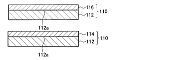
- the substrate 116 is disposed on the first glass substrate 112 to form the stacked body 110.
- the surface roughness (Ra) of the surface of the first glass substrate 112 in contact with the substrate 116 is preferably 2.0 nm or less, and 1.0 nm.
- the following is more preferable.
- the lower limit is not particularly limited, but 0 is most preferable. If it is the said range, adhesiveness with the board
- the surface roughness (Ra) is measured according to JIS B 0601 (revised in 2001).
- each layer (the 1st glass substrate 12, the board
- substrate 116 in the laminated body 110 are the structures similar to the said 1st glass substrate 12 and the board
- the first glass substrate 12 supports and reinforces the substrate 16, and the substrate 16 is deformed, scratched, or damaged during the manufacture of the electronic device member in the member forming step (step of manufacturing the electronic device member) described later. Prevent such as.
- the first glass substrate 12 is a glass substrate having a compaction (compaction value) of 80 ppm or less during heat treatment at 600 ° C. for 80 minutes.
- the compaction is preferably 70 ppm or less, more preferably 60 ppm or less, and even more preferably 50 ppm or less in that the production yield of the electronic device is more excellent (hereinafter simply referred to as “the point where the effect of the present invention is more excellent”).
- the point where the effect of the present invention is more excellent Although a minimum in particular is not restrict
- the above compaction is a glass heat shrinkage rate generated by relaxation of the glass structure during the heat treatment.
- the compaction means that two indentations are made on the surface of the glass substrate at a predetermined interval, and then the glass substrate is heated from room temperature to 600 ° C. at 100 ° C./hour, heated to 600 ° C. for 80 minutes. After holding, it means the shrinkage rate (ppm) of the distance between indentations when cooled to room temperature at 100 ° C./hour.
- the compaction in the present invention can be measured by the following method.
- the surface of the glass substrate is polished to obtain a 100 mm ⁇ 20 mm sample.
- the distance between the indentations is measured again, and the distance is B.
- the compaction is calculated from A and B thus obtained using the following formula.
- the range of the strain point of the first glass substrate 12 is not particularly limited, but is preferably 700 ° C. or higher and more preferably 710 ° C. or higher in terms of more excellent effects of the present invention. However, if the strain point is too high, a problem arises in terms of glass forming. 760 ° C. or lower is more preferable, and 750 ° C. or lower is further preferable.
- the strain point is a temperature at which viscous flow of glass cannot practically occur, corresponds to a lower limit temperature in a slow cooling region, and refers to a temperature corresponding to a viscosity of 10 14.5 dPa ⁇ s ⁇ poise ⁇ .
- the strain point is measured using a fiber elongation method defined in JIS-R3103 (2001) and ASTM-C336 (1971).
- the composition of the first glass substrate 12 is not particularly limited, but is preferably in the following range as the glass mother composition in terms of oxide-based mass percentage because the effects of the present invention are more excellent.
- SiO 2 50 to 73% Al 2 O 3 : 10.5-24%
- B 2 O 3 0 to 5%
- the composition range of each component will be described. If SiO 2 is less than 50% (expressed in terms of mass percentage based on oxide, the same applies unless otherwise specified), the strain point does not increase sufficiently, the thermal expansion coefficient increases, and the density increases. preferable. 53% or more is more preferable, 55% or more is more preferable, and 57% or more is particularly preferable. If it exceeds 73%, the solubility is lowered and the defoaming property is lowered, so 73% or less is preferable. 70% or less is more preferable, 67% or less is more preferable, and 65% or less is particularly preferable.
- Al 2 O 3 suppresses the phase separation of the glass, lowers the thermal expansion coefficient, and raises the strain point. However, if it is less than 10.5%, this effect does not appear, and other components that increase the expansion increase. As a result, thermal expansion increases. 10.5% or more is preferable, 15% or more is more preferable, and 17% or more is more preferable. If it exceeds 24%, the solubility of the glass may be deteriorated or the devitrification temperature may be increased, so 24% or less is preferable, and 22% or less is more preferable.
- B 2 O 3 can be added in an amount of 0% to 5% in order to improve the melting reactivity of the glass and to lower the devitrification temperature. In order to acquire said effect, 0.1% or more is preferable. However, if it is too much, the strain point is lowered. Therefore, 5% or less is preferable and 3% or less is more preferable.
- MgO has the characteristics that it does not increase the expansion in alkaline earth and does not excessively lower the strain point, and also improves the solubility.
- the MgO content is preferably 0% or more and 10% or less, but more preferably 1% or more. If it exceeds 10%, the devitrification temperature may increase, so it is preferably 10% or less, more preferably 7% or less, and even more preferably 6% or less.
- CaO has the characteristics that it does not increase the expansion in alkaline earth after MgO, and does not excessively lower the strain point, and also improves the solubility.
- the CaO content is preferably 0% or more and 14.5% or less, more preferably 1% or more, and further preferably 3% or more. If it exceeds 14.5%, the devitrification temperature may increase. 10% or less is more preferable, and 7% or less is more preferable.
- SrO is an optional component that improves the solubility without increasing the devitrification temperature of the glass.
- the SrO content is preferably 0% or more and 24% or less, but more preferably 1% or more. If it exceeds 24%, the expansion coefficient may increase. 12% or less is more preferable, and 9% or less is more preferable.
- BaO is not essential, but can be contained for improving solubility and resistance to devitrification. However, too much increases the expansion and density of the glass excessively, so 13.5% or less is preferable, 12% or less is more preferable, and 10% or less is more preferable.
- the content of BaO should be small, preferably 5% or less, preferably 1% or less, more preferably 0.5% or less, and substantially no content. Particularly preferred. “Substantially not contained” means not containing any inevitable impurities. On the other hand, when importance is attached to devitrification resistance, it is preferably 1% or more, more preferably 3% or more, and further preferably 5% or more.
- MgO, CaO, SrO, and BaO are less than 8% in total, solubility is poor. 8% or more is preferable and 10% or more is more preferable. 12% or more is more preferable, and 14% or more is particularly preferable. If it exceeds 29.5%, there is a possibility that the thermal expansion coefficient cannot be reduced, so 29.5% or less is preferable, 25% or less is more preferable, 23% or less is more preferable, and 21% or less is preferable. Particularly preferred.
- a component for adjusting physical properties and a clarifying agent can be added within the range not impairing the features of the present invention.
- components for adjusting the physical properties Fe 2 O 3 , ZnO, ZrO 2 , TiO 2 , Nb 2 O 5 , Ta 2 O 5 , Y 2 O 3 , La 2 O 3 , Gd 2 O 3 , P 2
- O 5 and a clarifying agent include SnO 2 , SO 3 , Cl, and F. Any of them can be contained in a range of less than 1%.
- Alkali metal oxides such as Li 2 O, Na 2 O, and K 2 O may be mixed as an inevitable impurity of the raw material or added to promote melting. These cause contamination by alkali ions in the TFT manufacturing process, and as a result, there is a possibility of deteriorating TFT characteristics. Therefore, it is preferable not to contain as much as possible. Specifically, 0.1% or less is preferable. 0.08% or less is more preferable, 0.05% or less is more preferable, and 0.03% or less is particularly preferable.
- the glass used for the first glass substrate 12 or the first glass substrate 112 has a high Young's modulus in order to reduce bending during transport of the laminated substrate. 77 GPa or more is preferable, 80 GPa or more is more preferable, and 82 GPa or more is particularly preferable.
- the glass used for the first glass substrate 12 or the first glass substrate 112 is scratched, it is possible to reduce the strength during recycling or to cause non-uniformity during ultraviolet light irradiation described later. There is sex. Therefore, it is preferable that the glass of the first glass substrate 12 or the first glass substrate 112 has a higher Vickers hardness. 580 or more is preferable, 590 or more is more preferable, and 600 or more is more preferable.
- the liquid crystal is irradiated by, for example, ultraviolet light through the first glass substrate 12.
- the ultraviolet transmittance of the glass is high.
- the external transmittance of 300 nm is preferably 40% or more in terms of 0.5 mm thickness. More preferably, it is 50% or more, more preferably 60% or more, and particularly preferably 70% or more.
- the thickness of the first glass substrate 12 may be thicker or thinner than the substrate 16, but is usually thinner than the substrate 16.
- the thickness of the first glass substrate 12 is selected based on the thickness of the substrate 16, the thickness of the adhesion layer 14, and the thickness of the stacked body 100.
- the first The thickness of the glass substrate 12 is 0.4 mm.
- the thickness of the first glass substrate 12 is preferably 0.2 to 0.5 mm, and is preferably thicker than the substrate 16.
- the manufacturing method of the first glass substrate 12 is not particularly limited as long as the glass substrate showing the above-described compaction can be obtained. Among these, it is easy to adjust the compaction by melting a glass raw material to obtain a molten glass, a molding process for molding the molten glass obtained by the melting process into a plate-like glass ribbon, and a molding process. And a slow cooling step of slowly cooling the formed glass ribbon.
- molten glass is obtained by melting glass raw materials.
- a glass raw material is prepared so as to have the composition of the obtained glass plate, the glass raw material is continuously charged into a melting furnace, and heated to about 1450 to 1650 ° C. to obtain a molten glass.
- the molten glass obtained in the melting step is formed into a plate-like glass ribbon (ribbon-like glass plate). More specifically, it is formed into a glass ribbon having a predetermined plate thickness by a float method or a fusion method.
- the plate-shaped glass ribbon obtained in the molding step is slowly cooled.
- a method of controlling the cooling rate in the slow cooling step is preferable.
- the average cooling rate can be adjusted, for example, in the range of 15 to 600 ° C./min.
- the temperature is preferably 20 to 400 ° C./min, more preferably 30 to 300 ° C./min, and further preferably 30 to 100 ° C./min.
- a specific cooling means is not specifically limited, A conventionally well-known cooling method may be used. For example, a method using a heating furnace having a temperature gradient can be mentioned.
- the substrate 16 has a first main surface 16a in contact with the adhesion layer 14, and an electronic device member is provided on the second main surface 16b opposite to the adhesion layer 14 side. That is, the substrate 16 is a substrate used for forming an electronic device described later.
- substrate 16 is not restrict
- the type of the second glass substrate may be a common one, for example, a glass substrate for a display device such as an LCD or an OLED. Can be mentioned.
- the second glass substrate is excellent in chemical resistance and moisture permeability and has a low heat shrinkage rate.
- As an index of the heat shrinkage rate a linear expansion coefficient defined in JIS R 3102 (revised in 1995) is used.
- the second glass substrate is obtained by melting a glass raw material and molding the molten glass into a plate shape.
- a molding method may be a general one, and for example, a float method, a fusion method, a slot down draw method, or the like is used.
- the second glass substrate having a particularly small thickness can also be obtained by heating the glass once formed into a plate shape to a moldable temperature and stretching it by means of stretching or the like to make it thin (redraw method). .
- the thickness of the substrate 116 is preferably 0.1 mm or less, and more preferably 0.05 mm or less.
- it is preferably 0.001 mm or more, more preferably 0.005 mm or more, and further preferably 0.01 mm or more.
- the glass of the first glass substrate 112 when a device is manufactured in such a process is required to have a high ultraviolet transmittance. This is because when the substrate 116 directly formed on the first glass substrate 112 is peeled off, ultraviolet rays are irradiated from the first glass substrate 112 side. Therefore, the ultraviolet transmittance of the glass of the first glass substrate 112 is preferably 40% or more, more preferably 50% or more, and further preferably 60% or more, as the external transmittance at a wavelength of 300 nm, regardless of the plate thickness. % Or more is particularly preferable.
- the plate thickness of the first glass substrate 112 is not particularly limited, but if the plate thickness is too thin, the deflection becomes large and a problem occurs during transportation. Therefore, the thickness is preferably 0.4 mm or more, and more preferably 0.5 mm or more. On the other hand, if it is too thick, the weight of the substrate becomes too large and the load on the transport device becomes large.
- the adhesion layer 14 prevents the displacement of the substrate 16 until the operation for separating the substrate 16 and the first glass substrate 12 is performed, and prevents the substrate 16 and the like from being damaged by the separation operation.
- the surface 14a of the adhesion layer 14 that contacts the substrate 16 is detachably laminated (adhered) to the first main surface 16a of the substrate 16.
- the adhesion layer 14 is bonded to the first main surface 16 a of the substrate 16 with a weak bonding force, and the peel strength (y) at the interface is between the adhesion layer 14 and the first glass substrate 12. Lower than the peel strength (x) at the interface.
- the adhesion layer 14 is in close contact with the first main surface 16a of the substrate 16, but has a surface characteristic that allows the substrate 16 to be easily peeled off. That is, the adhesion layer 14 is bonded to the first main surface 16a of the substrate 16 with a certain amount of bonding force to prevent the displacement of the substrate 16, and at the same time, when the substrate 16 is peeled off, The 16 is bonded with a bonding force that can be easily peeled without breaking.
- the type of the adhesion layer 14 is not particularly limited, and may be an organic layer made of a resin or the like, or an inorganic layer. Hereinafter, each case will be described in detail.
- the organic layer is preferably a resin layer containing a predetermined resin.
- the kind of resin forming the resin layer is not particularly limited, and examples thereof include silicone resin, polyimide resin, acrylic resin, polyolefin resin, polyurethane resin, and fluorine resin. Several types of resins can be mixed and used. Of these, silicone resins, polyimide resins, and fluorine resins are preferable.
- addition reaction type silicone a curable composition which contains a main agent and a crosslinking agent and cures in the presence of a catalyst such as a platinum-based catalyst can be suitably used. Curing of the addition reaction type silicone is accelerated by heat treatment.
- the main component in the addition-reactive silicone is preferably an organopolysiloxane having an alkenyl group (such as a vinyl group) bonded to a silicon atom (that is, an organoalkenylpolysiloxane, preferably a straight chain). These are the cross-linking points.
- the cross-linking agent in the addition reaction type silicone is preferably an organopolysiloxane having a hydrogen atom (hydrosilyl group) bonded to a silicon atom (that is, an organohydrogenpolysiloxane, preferably linear). Hydrosilyl groups and the like serve as crosslinking points.
- the addition reaction type silicone is cured by the addition reaction between the crosslinking points of the main agent and the crosslinking agent.
- the molar ratio of the hydrogen atom bonded to the silicon atom of the organohydrogenpolysiloxane to the alkenyl group of the organoalkenylpolysiloxane is 0.5 to 2 in that the heat resistance derived from the crosslinked structure is more excellent. preferable.
- the condensation reaction type silicone includes a hydrolyzable organosilane compound as a monomer or a mixture thereof (monomer mixture), or a partial hydrolysis condensate obtained by subjecting a monomer or monomer mixture to a partial hydrolysis condensation reaction (organopolysiloxane). Can be suitably used.
- a silicone resin can be formed by proceeding a hydrolysis / condensation reaction (sol-gel reaction) using this condensation reaction type silicone.
- A represents a diamine residue obtained by removing an amino group from diamines, and preferably comprises at least one group selected from the group consisting of groups represented by the following formulas (A1) to (A8).
- the polyimide described above can be used not only as an organic layer but also as a second substrate (substrate 116).
- the thickness of the organic layer is not particularly limited, but is preferably 1 to 100 ⁇ m, more preferably 5 to 30 ⁇ m, and even more preferably 7 to 20 ⁇ m. This is because when the thickness of the organic layer is within such a range, the adhesion between the organic layer and the first glass substrate or the substrate is sufficient.
- the material constituting the inorganic layer is not particularly limited, but preferably includes at least one selected from the group consisting of oxides, nitrides, oxynitrides, carbides, carbonitrides, silicides, and fluorides. Especially, it is preferable that an oxide is included at the point which the peelability of the board
- silicon nitride oxide SiN x O y
- titanium oxide TiO 2
- indium oxide In 2 O 3
- indium cerium oxide ICO
- tin oxide SnO 2
- zinc oxide ZnO
- Gallium oxide Ga 2 O 3
- indium tin oxide ITO
- indium zinc oxide IZO
- zinc oxide tin ZTO
- gallium-doped zinc oxide GZO
- silicides include silicides of one or more elements selected from Mo, W, and Cr.
- fluorides include fluorides of one or more elements selected from Mg, Y, La, and Ba.
- magnesium fluoride MgF 2
- MgF 2 magnesium fluoride
- the manufacturing method of the laminate 100 according to the first embodiment of the present invention is not particularly limited, and a known method can be adopted.
- the adhesion layer forming step corresponds to a carrier substrate manufacturing step.
- the adhesion layer forming step and the laminating step will be described in detail.
- the adhesion layer 14 is an organic layer
- a curable resin composition containing a curable resin is applied on the first glass substrate 12, and the curable resin composition is applied. Is cured to form the adhesion layer 14 fixed on the first glass substrate 12 (application method), or the film-like adhesion layer 14 is fixed to the surface of the first glass substrate 12 (pasting method). Etc.
- coating method is preferable at the point which the adhesive strength with respect to the 1st glass substrate 12 of the contact
- examples of the method of forming the curable resin composition layer on the surface of the first glass substrate 12 include a method of coating the curable resin composition on the glass substrate.
- examples of the coating method include spray coating, die coating, spin coating, dip coating, roll coating, bar coating, screen printing, and gravure coating.
- the curing method is not particularly limited, and optimum curing conditions are selected depending on the resin used. Usually, heat treatment is adopted as a curing method.
- a resin composition containing a resin component such as a phenol resin is applied on the first glass substrate 12 and subjected to a sintering treatment to perform carbonization.
- the method of making it also includes.
- manufacturing conditions optimum conditions are appropriately selected according to the materials used.
- the substrate 16 is laminated on the surface of the adhesion layer 14 obtained in the adhesion layer forming step, and the laminate 100 including the first glass substrate 12, the adhesion layer 14, and the substrate 16 in this order is obtained. It is a process.
- the method for laminating the substrate 16 on the adhesion layer 14 is not particularly limited, and a known method can be adopted. For example, a method of stacking the substrate 16 on the surface of the adhesion layer 14 under a normal pressure environment can be mentioned. If necessary, after the substrate 16 is overlaid on the surface of the adhesion layer 14, the substrate 16 may be bonded to the adhesion layer 14 using a roll or a press. Air bubbles mixed between the adhesive layer 14 and the substrate 16 are relatively easily removed by pressure bonding using a roll or a press, which is preferable.
- an electronic device including a substrate and an electronic device member (hereinafter, also referred to as “membered substrate” as appropriate) is manufactured using the above-described laminate.
- membered substrate an electronic device member
- the manufacturing method of the electronic device using the laminated body which has the adhesion layer mentioned above is explained in full detail.
- a member for electronic device is formed on a substrate in the above-described laminate to manufacture a laminate with a member for electronic device.
- a method of separating the electronic device member-attached laminate into an electronic device (substrate with a member) and a carrier substrate using the substrate-side interface of the adhesion layer as a release surface is preferable.
- the step of forming the electronic device member on the substrate in the laminate to produce the laminate with the electronic device member is a member forming step, and the substrate side interface of the adhesion layer is peeled from the laminate with the electronic device member
- the step of separating the substrate with the member and the carrier substrate as a surface is called a separation step.
- a member formation process is a process of forming the member for electronic devices on the board
- the electronic device member 20 is a member that is formed on the substrate 16 in the laminate 100 and constitutes at least a part of the electronic device. More specifically, as the electronic device member 20, a member used for an electronic component such as a display panel, a solar cell, a thin film secondary battery, or a semiconductor wafer having a circuit formed on the surface (for example, Display member, solar cell member, thin film secondary battery member, electronic component circuit).
- a silicon type includes a transparent electrode such as tin oxide of a positive electrode, a silicon layer represented by p layer / i layer / n layer, a metal of a negative electrode, and the like. And various members corresponding to the dye-sensitized type, the quantum dot type, and the like.
- a transparent electrode such as a metal or a metal oxide of a positive electrode and a negative electrode, a lithium compound of an electrolyte layer, a metal of a current collecting layer, a resin as a sealing layer, etc.
- various members corresponding to nickel hydrogen type, polymer type, ceramic electrolyte type and the like can be mentioned.
- a circuit for an electronic component in a CCD or CMOS, a metal of a conductive part, a silicon oxide or a silicon nitride of an insulating part, and the like, various sensors such as a pressure sensor and an acceleration sensor, a rigid printed board, a flexible printed board And various members corresponding to a rigid flexible printed circuit board.
- the electronic device member 20 preferably includes low-temperature polysilicon (LTPS: Low-temperature poly silicon). That is, the member forming step preferably includes a step of manufacturing low-temperature polysilicon. Especially, it is more preferable that this member forming step includes a step of manufacturing a thin film transistor containing low-temperature polysilicon.
- LTPS Low-temperature polysilicon
- Low temperature polysilicon is polysilicon obtained by crystallizing silicon by using amorphous silicon as a precursor and applying crystallization energy by laser annealing, furnace annealing, or the like.
- amorphous silicon is often heated to 450 ° C. or higher, in other words, the process temperature is often 450 ° C. or higher.
- the electronic device member 20 is not all of the members finally formed on the second main surface 16b of the substrate 16 (hereinafter referred to as “all members”), but a part of all members (hereinafter referred to as “partial members”). ").
- the substrate with partial members peeled off from the adhesion layer 14 can be used as a substrate with all members (corresponding to an electronic device described later) in the subsequent steps.
- an electronic device may be formed on the peeling surface (first main surface 16a) of the substrate with all members peeled from the adhesion layer 14.
- an electronic device can also be manufactured by assembling a laminate with all members and then peeling the carrier substrate 10 from the laminate with all members. Furthermore, it is also possible to assemble using two laminates with all members, and then peel off the two carrier substrates 10 from the laminate with all members to produce a member-equipped substrate having two glass substrates.
- an organic EL structure is formed on the surface of the laminate 100 opposite to the adhesion layer 14 side of the substrate 16 (corresponding to the second main surface 16b of the substrate 16).
- a transparent electrode further deposit a hole injection layer, a hole transport layer, a light emitting layer, an electron transport layer, etc. on the surface on which the transparent electrode is formed, use a sealing plate to form a back electrode
- Various layer formation and processing such as sealing are performed. Specific examples of the layer formation and processing include film formation processing, vapor deposition processing, sealing plate adhesion processing, and the like.
- a TFT-LCD when manufacturing a TFT-LCD, it is formed on the second main surface 16b of the substrate 16 of the multilayer body 100 using a resist solution by a general film forming method such as a CVD method or a sputtering method.
- TFT thin film transistor
- There are various processes such as a CF forming process for forming a color filter (CF), a laminating process for laminating a laminated body with TFT obtained in the TFT forming process and a laminated body with CF obtained in the CF forming process.
- the thin film transistor forming surface of the laminated body with TFT and the color filter forming surface of the laminated body with CF are opposed to each other, and are bonded using a sealant (for example, an ultraviolet curable sealant for cell formation).
- a sealant for example, an ultraviolet curable sealant for cell formation.
- a liquid crystal material is injected into a cell formed by the laminate with TFT and the laminate with CF.
- the method for injecting the liquid crystal material include a reduced pressure injection method and a drop injection method.
- the separation step As shown in FIG. 4B, from the laminate 22 with the electronic device member obtained in the member forming step, the interface between the adhesion layer 14 and the substrate 16 is used as the release surface, and the electronic device member.
- This is a step of separating the substrate 20 (substrate with member) 20 and the carrier substrate 10 to obtain a member-attached substrate (electronic device) 24 including the electronic device member 20 and the substrate 16.
- the electronic device member 20 on the substrate 16 at the time of peeling is a part of the formation of all necessary constituent members, the remaining constituent members can be formed on the substrate 16 after separation.
- the method for peeling the substrate 16 and the carrier substrate 10 is not particularly limited. Specifically, for example, a sharp blade-like object is inserted into the interface between the substrate 16 and the adhesion layer 14 to give a trigger for peeling, and then peeled off by spraying a mixed fluid of water and compressed air. be able to.
- the electronic device member-attached laminate 22 is placed on a surface plate so that the carrier substrate 10 is on the upper side and the electronic device member 20 side is on the lower side, and the electronic device member 20 side is vacuum-adsorbed on the surface plate. (In the case where carrier substrates are laminated on both surfaces, the steps are sequentially performed).
- the blade is first inserted into the interface between the substrate 16 and the adhesion layer 14. Thereafter, the carrier substrate 10 side is sucked by a plurality of vacuum suction pads, and the vacuum suction pads are raised in order from the vicinity of the place where the blade is inserted.
- the fragments of the adhesion layer 14 are electrostatically adsorbed to the substrate with member 24 by controlling spraying and humidity with an ionizer. It can be suppressed more.
- a panel for a display device having a glass substrate and a member for a display device As the substrate 24 with a member manufactured by the above method, a panel for a display device having a glass substrate and a member for a display device, a solar cell having a glass substrate and a member for a solar cell, and a member for a glass substrate and a thin film secondary battery.
- Examples include a thin film secondary battery, an electronic component having a glass substrate and an electronic device member.
- the display device panel include a liquid crystal panel, an organic EL panel, a plasma display panel, a field emission panel, and the like.
- Table 1 is a table showing compaction and the like of glass substrates having 12 kinds of compositions.
- the raw materials of each component were prepared so as to have the target composition shown below, and melted at a temperature of 1500 to 1600 ° C. using a platinum crucible to obtain a molten glass. In melting, the mixture was stirred using a platinum stirrer to homogenize the glass. Next, molten glass was poured out, formed into a plate having a thickness of 0.3 mm, and then slowly cooled to produce a first glass substrate. In addition, as slow cooling conditions, it cooled by the average cooling rate (degreeC / min) of Table 1.
- the Young's modulus was measured by an ultrasonic pulse method for glass having a thickness of 0.5 to 10 mm according to a method defined in JIS Z 2280 (1993).
- the ultraviolet transmittance was measured at a wavelength of 300 nm using a UV-visible near-infrared spectrophotometer U4100 manufactured by Hitachi High-Tech Science Co., Ltd. with respect to glass having a thickness of 0.5 mm whose surfaces were optically polished.
- the strain point was measured by the method described above.
- surface represents the compaction (shrinkage
- V 0 is the molar volume of the glass at the processing time
- V ⁇ is the equilibrium molar volume at the processing temperature
- V ( ⁇ ) is the molar volume of the glass at the conversion time ⁇
- C is the compaction (unit: ppm)
- ⁇ L is the amount of change of the glass length before and after treatment
- ⁇ is the relaxation time constant
- ⁇ is a parameter indicating the spread of the relaxation time constant.
- Table 2 is a table showing the result of measuring the compaction by subjecting the glass substrate of Table 1 to heat treatment multiple times (three times). Using the first glass substrates 1 to 12, the compaction of the glass substrate after each heat treatment when the heat treatment under the following heating conditions was performed a plurality of times was calculated.
- the first column represents the compaction (ppm) of the glass substrate after performing the following heat treatment once.
- the second column shows the compaction after the second heat treatment is performed after the glass substrate subjected to the first heat treatment is cooled to room temperature.
- the third column shows the compaction after performing the third heat treatment after cooling the glass substrate subjected to the second heat treatment to room temperature.
- the glass substrate is heated from room temperature to 450 ° C. over 5 minutes, then held at 450 ° C. for 20 minutes, then cooled to room temperature for 5 minutes, and further the glass substrate is raised from room temperature to 600 ° C. over 5 minutes. Then, the mixture was kept at 600 ° C. for 5 minutes, and then cooled in 5 minutes until reaching room temperature.
- Alkenyl group-containing organopolysiloxane (number average molecular weight: 2000, number of alkenyl groups: 2 or more) (100 parts by mass) and hydrogen polysiloxane (number average molecular weight: 2000, number of hydrosilyl groups: 2 or more) (6.7 parts by mass).
- the mixing molar ratio of the alkenyl group in the alkenyl group-containing organopolysiloxane and the hydrosilyl group in the hydrogen polysiloxane (number of moles of hydrosilyl group / number of moles of alkenyl group) was 0.4 / 1. It was.
- the second glass substrate a glass plate made of non-alkali borosilicate glass (length 200 mm, width 200 mm, plate thickness 0.2 mm, linear expansion coefficient 38 ⁇ 10 ⁇ 7 / ° C., trade name “AN100” manufactured by Asahi Glass Co., Ltd.) )It was used.
- the first glass substrate and the second glass substrate were in close contact with the silicone resin layer without generating bubbles, and there was no distortion defect.
- the peel strength at the interface between the silicone resin layer and the first glass substrate layer was greater than the peel strength at the interface between the second glass substrate layer and the silicone resin layer.
- an electronic device was manufactured on the second glass substrate of the glass laminate A according to the following method.
- an LTPS process using an excimer laser annealing method was used.
- an amorphous silicon film was formed.
- a thin film transistor circuit was formed by performing a dehydrogenation process, a laser irradiation, and an activation process, and forming and patterning various wirings such as a gate electrode, a source, and a drain electrode, and forming an interlayer insulating film and the like.
- the process whose manufacturing process temperature is 500 degreeC or more was included.
- the vacuum suction pad was pulled up while spraying a static eliminating fluid continuously from the ionizer toward the formed gap.
- the silicone resin layer is separated from the second glass substrate together with the first glass substrate.
- the peel strength (x) at the interface between the layer of the first glass substrate and the silicone resin layer is determined as follows. It was confirmed that the peel strength (y) at the interface of the substrate was higher.
- a glass laminate A was manufactured according to the same procedure as described above, and an electronic device was manufactured according to the same procedure as described above. This process was repeated twice to produce an electronic device. In addition, the several glass laminated body A was prepared and the said process was implemented, respectively.
Landscapes
- Chemical & Material Sciences (AREA)
- Engineering & Computer Science (AREA)
- Life Sciences & Earth Sciences (AREA)
- Chemical Kinetics & Catalysis (AREA)
- General Chemical & Material Sciences (AREA)
- Geochemistry & Mineralogy (AREA)
- Materials Engineering (AREA)
- Organic Chemistry (AREA)
- Ceramic Engineering (AREA)
- Mechanical Engineering (AREA)
- Laminated Bodies (AREA)
- Crystallography & Structural Chemistry (AREA)
- Electroluminescent Light Sources (AREA)
- Liquid Crystal (AREA)
- Glass Compositions (AREA)
- Microelectronics & Electronic Packaging (AREA)
- Encapsulation Of And Coatings For Semiconductor Or Solid State Devices (AREA)
- Structures Or Materials For Encapsulating Or Coating Semiconductor Devices Or Solid State Devices (AREA)
Abstract
Description
また、本発明は、上記キャリア基板を含む積層体、および、電子デバイスの製造方法に関する。
コンパクション:第1ガラス基板を室温より100℃/時間で昇温し600℃で80分間の加熱処理をしてから、100℃/時間で室温まで冷却した場合の収縮率
また、第1の態様において、第1ガラス基板の歪点が700℃以上であることが好ましい。
SiO2:50~73%
Al2O3:10.5~24%
B2O3:0~5%
MgO:0~10%
CaO:0~14.5%
SrO:0~24%
BaO:0~13.5%
MgO+CaO+SrO+BaO:8~29.5%
また、第2の態様において、基板が第2ガラス基板であることが好ましい。
電子デバイス用部材付き積層体からキャリア基板を除去し、基板と電子デバイス用部材とを有する電子デバイスを得る分離工程と、を備える電子デバイスの製造方法である。
また、第3の態様において、電子デバイス用部材を形成する際にプロセス温度が450℃以上である工程を含むことが好ましい。
また、本発明によれば、上記キャリア基板を含む積層体、および、該積層体を用いた電子デバイスの製造方法を提供することもできる。
本発明者らは、キャリア基板を複数回再利用した際に、電子デバイスの歩留まりが低下していく理由について検討を行ったところ、キャリア基板の熱収縮(コンパクション)が影響していることを知見している。
図2に示すように、積層体100は、第1ガラス基板12の層と基板16の層とそれらの間に密着層14が存在する積層体である。密着層14は、その一方の面が第1ガラス基板の層に接すると共に、その他方の面が基板16の第1主面16aに接している。なお、基板16は、剥離可能に密着層14上に積層されている。
第1ガラス基板12および密着層14からなるキャリア基板10は、液晶パネルなどの電子デバイス用部材を製造する部材形成工程において、基板16を補強する補強板として機能する。
この実施態様の場合、図3に示すように、第1ガラス基板112上に基板116が配置されて、積層体110が形成される。
表面粗さ(Ra)はJIS B 0601(2001年改正)に従って測定される。
なお、積層体110中の第1ガラス基板112および基板116は、上記第1ガラス基板12および基板16と同様の構成であるため、説明を省略する。
第1ガラス基板12は、基板16を支持して補強し、後述する部材形成工程(電子デバイス用部材を製造する工程)において電子デバイス用部材の製造の際に基板16の変形、傷付き、破損などを防止する。
コンパクションが80ppm超の場合、電子デバイスの製造歩留まりが劣る。
ガラス基板の表面を研磨加工して100mm×20mmの試料を得る。該試料の表面に点状の圧痕を長辺方向に2箇所、間隔A(A=95mm)で打つ。
次に該試料を室温から600℃まで昇温速度100℃/時(=1.6℃/分)で加熱し、600℃で80分間保持した後、降温速度100℃/時で室温まで冷却する。そして、再度、圧痕間距離を測定し、その距離をBとする。このようにして得たA、Bから下記式を用いてコンパクションを算出する。なお、A、Bは光学顕微鏡を用いて測定する。
コンパクション[ppm]=(A-B)/A×106
SiO2:50~73%
Al2O3:10.5~24%
B2O3:0~5%
MgO:0~10%
CaO:0~14.5%
SrO:0~24%
BaO:0~13.5%
MgO+CaO+SrO+BaO:8~29.5%
SiO2は50%(酸化物基準の質量百分率表示、特記しないかぎり以下同じ)未満では、歪点が充分に上がらず、かつ、熱膨張係数が増大し、密度が上昇するので、50%以上が好ましい。53%以上がより好ましく、55%以上がさらに好ましく、57%以上が特に好ましい。73%超では、溶解性が低下し、脱泡性が低下するため、73%以下が好ましい。70%以下がより好ましく、67%以下がさらに好ましく、65%以下が特に好ましい。
ここで、MgO含有量は0%以上10%以下であることが好ましいが、1%以上がより好ましい。10%を超えると、失透温度が上昇するおそれがあるので、10%以下が好ましく、7%以下がより好ましく、6%以下がさらに好ましい。
ここで、CaOの含有量は0%以上14.5%以下であることが好ましいが、1%以上であることがより好ましく、3%以上がさらに好ましい。14.5%を超えると、失透温度が上昇するおそれがある。10%以下がより好ましく、7%以下がさらに好ましい。
ここで、SrO含有量は0%以上24%以下であることが好ましいが、1%以上がより好ましい。24%を超えると膨脹係数が増大するおそれがある。12%以下がより好ましく、9%以下がさらに好ましい。
一方、耐失透性を重視する場合には、1%以上が好ましく、3%以上がより好ましく、5%以上がさらに好ましい。
また、具体的な冷却手段は特に限定されず、従来公知の冷却方法であってよい。例えば温度勾配を持った加熱炉を用いる方法が挙げられる。
基板16は、第1主面16aが密着層14と接し、密着層14側とは反対側の第2主面16bに電子デバイス用部材が設けられる。つまり、基板16は、後述する電子デバイスの形成するために使用される基板である。
基板16の種類は特に制限されず、ガラス基板、樹脂基板、金属基板などが挙げられる。
また、基板16の厚さは、基板16の製造が容易であること、基板16の取り扱いが容易であることなどの理由から、0.03mm以上であることが好ましい。
密着層14は、基板16と第1ガラス基板12とを分離する操作が行われるまで基板16の位置ずれを防止すると共に、基板16などが分離操作によって破損するのを防止する。密着層14の基板16と接する表面14aは、基板16の第1主面16aに剥離可能に積層(密着)する。上述したように、密着層14は基板16の第1主面16aに弱い結合力で結合しており、その界面の剥離強度(y)は、密着層14と第1ガラス基板12との間の界面の剥離強度(x)よりも低い。
有機層としては、所定の樹脂を含む樹脂層であることが好ましい。樹脂層を形成する樹脂の種類は特に限定されず、例えば、シリコーン樹脂、ポリイミド樹脂、アクリル樹脂、ポリオレフィン樹脂、ポリウレタン樹脂、またはフッ素系樹脂等が挙げられる。いくつかの種類の樹脂を混合して用いることもできる。中でもシリコーン樹脂、ポリイミド樹脂、フッ素系樹脂が好ましい。
白金族金属系触媒(ヒドロシリル化用白金族金属触媒)は、上記オルガノアルケニルポリシロキサン中のアルケニル基と、上記オルガノハイドロジェンポリシロキサン中の水素原子とのヒドロシリル化反応を、進行・促進させるための触媒である。白金族金属系触媒としては、白金系、パラジウム系、ロジウム系などの触媒が挙げられ、特に白金系触媒として用いることが経済性、反応性の点から好ましい。
この縮合反応型シリコーンを用いて、加水分解・縮合反応(ゾルゲル反応)を進行させることにより、シリコーン樹脂を形成することができる。
ポリイミド樹脂の構造は特に制限されないが、下記式(1)で表される、テトラカルボン酸類の残基(X)とジアミン類の残基(A)とを有する繰り返し単位からなることが好ましい。


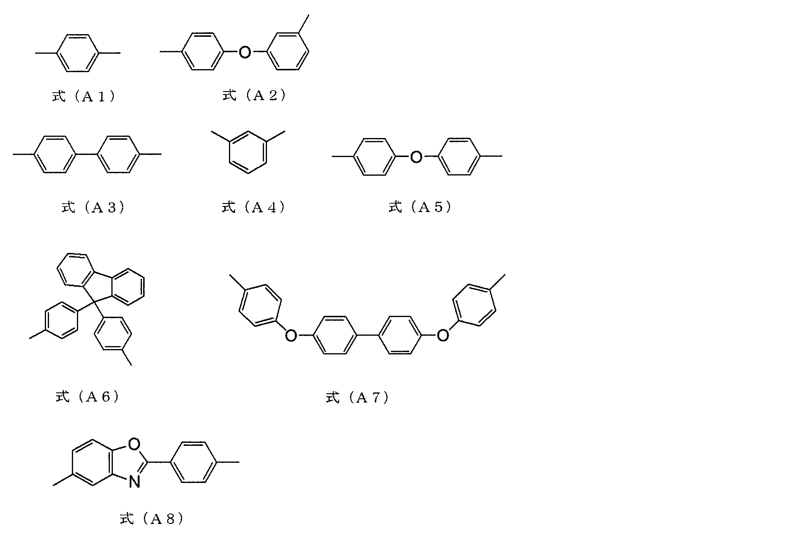
無機層を構成する材料は特に制限されないが、例えば、酸化物、窒化物、酸窒化物、炭化物、炭窒化物、珪化物および弗化物からなる群から選ばれる少なくとも1つを含むことが好ましい。なかでも、基板16の剥離性がより優れる点で、酸化物を含むことが好ましい。
なお、炭化物としては、いわゆるカーボン材料であってもよく、例えば、フェノール樹脂などの樹脂成分を焼結して得られる炭化物であってもよい。
弗化物(好ましくは、金属弗化物)としては、例えば、Mg、Y、La、Baから選ばれる1種以上の元素の弗化物が挙げられる。例えば、弗化マグネシウム(MgF2)などが挙げられる。
RaはJIS B 0601(2001年改正)に従って測定される。
本発明の第1実施態様の積層体100の製造方法は特に制限されず、公知の方法を採用できるが、通常、第1ガラス基板12上に密着層14を形成する密着層形成工程と、密着層14上に基板16を積層して積層体100とする積層工程とを有する。なお、上記密着層形成工程は、キャリア基板の製造工程に該当する。
以下、密着層形成工程、および、積層工程について詳述する。
密着層形成工程は、第1ガラス基板12上に密着層14を形成する工程である。密着層14を形成する方法は特に制限されず、公知の方法を採用でき、密着層14を構成する材料の種類によって異なる。
硬化方法は特に制限されず、使用される樹脂によって最適な硬化条件が選択される。通常、硬化方法としては、加熱処理が採用される。
例えば、フッ素系樹脂を含む密着層を作製する方法は特に制限されず、フッ素系樹脂を含む組成物を用いて密着層を作製する方法や、フッ素系のガスを用いてプラズマを照射することで対象物表面に密着層を作製する方法が挙げられる。
製造条件は、使用される材料に応じて、適宜最適な条件が選択される。
積層工程は、上記の密着層形成工程で得られた密着層14の面上に基板16を積層し、第1ガラス基板12と密着層14と基板16とをこの順で備える積層体100を得る工程である。
例えば、常圧環境下で密着層14の表面上に基板16を重ねる方法が挙げられる。なお、必要に応じて、密着層14の表面上に基板16を重ねた後、ロールやプレスを用いて密着層14に基板16を圧着させてもよい。ロールまたはプレスによる圧着により、密着層14と基板16の層との間に混入している気泡が比較的容易に除去されるので好ましい。
基板16を積層する際には、密着層14に接触する基板16の表面を十分に洗浄し、クリーン度の高い環境で積層することが好ましい。クリーン度が高いほど、基板16の平坦性は良好となるので好ましい。
本発明の積層体(上述した第1実施態様の積層体100および第2実施態様の積層体110)は、種々の用途に使用することができ、例えば、後述する表示装置用パネル、PV、薄膜2次電池、表面に回路が形成された半導体ウェハ等の電子部品を製造する用途などが挙げられる。なお、該用途では、積層体100が高温条件(例えば、500℃以上)で曝される(例えば、20分以上)場合が多い。つまり、電子デバイスを形成する際にプロセス温度が500℃以上である工程が含まれる場合が多い。
本発明においては、上述した積層体を用いて、基板と電子デバイス用部材とを含む電子デバイス(以後、適宜「部材付き基板」とも称する)が製造される。
以下では、上述した密着層を有する積層体を用いた電子デバイスの製造方法について詳述する。
以下に、各工程で使用される材料および手順について詳述する。
部材形成工程は、上記積層工程において得られた積層体100中の基板16上に電子デバイス用部材を形成する工程である。より具体的には、図4(A)に示すように、基板16の第2主面16b(露出表面)上に電子デバイス用部材20を形成し、電子デバイス用部材付き積層体22を得る。
まず、本工程で使用される電子デバイス用部材20について詳述し、その後工程の手順について詳述する。
電子デバイス用部材20は、積層体100中の基板16上に形成され電子デバイスの少なくとも一部を構成する部材である。より具体的には、電子デバイス用部材20としては、表示装置用パネル、太陽電池、薄膜2次電池、または、表面に回路が形成された半導体ウェハ等の電子部品などに用いられる部材(例えば、表示装置用部材、太陽電池用部材、薄膜2次電池用部材、電子部品用回路)が挙げられる。
上述した電子デバイス用部材付き積層体22の製造方法は特に限定されず、電子デバイス用部材の構成部材の種類に応じて従来公知の方法にて、積層体100の基板16の第2主面16b上に、電子デバイス用部材20を形成する。
なお、TFTやCFを形成する前に、必要に応じて、基板16の第2主面16bを洗浄してもよい。洗浄方法としては、周知のドライ洗浄やウェット洗浄を用いることができる。
分離工程は、図4(B)に示すように、上記部材形成工程で得られた電子デバイス用部材付き積層体22から、密着層14と基板16との界面を剥離面として、電子デバイス用部材20が積層した基板16(部材付き基板)と、キャリア基板10とに分離して、電子デバイス用部材20および基板16を含む部材付き基板(電子デバイス)24を得る工程である。
剥離時の基板16上の電子デバイス用部材20が必要な全構成部材の形成の一部である場合には、分離後、残りの構成部材を基板16上に形成することもできる。
また、キャリア基板10は、新たなガラス基板と積層して、本発明の積層体100を製造することができる。
表1は、12種類の組成のガラス基板のコンパクション等を示した表である。各成分の原料を以下に示す目標組成になるように調合し、白金坩堝を用いて1500~1600℃の温度で溶解して溶融ガラスを得た。溶解にあたっては、白金スターラを用い撹拌しガラスの均質化を行った。次いで溶融ガラスを流し出し、板厚0.3mmの板状に成形後徐冷し、第1ガラス基板を製造した。なお、徐冷条件としては、表1に記載の平均冷却速度(℃/min)にて冷却を行った。
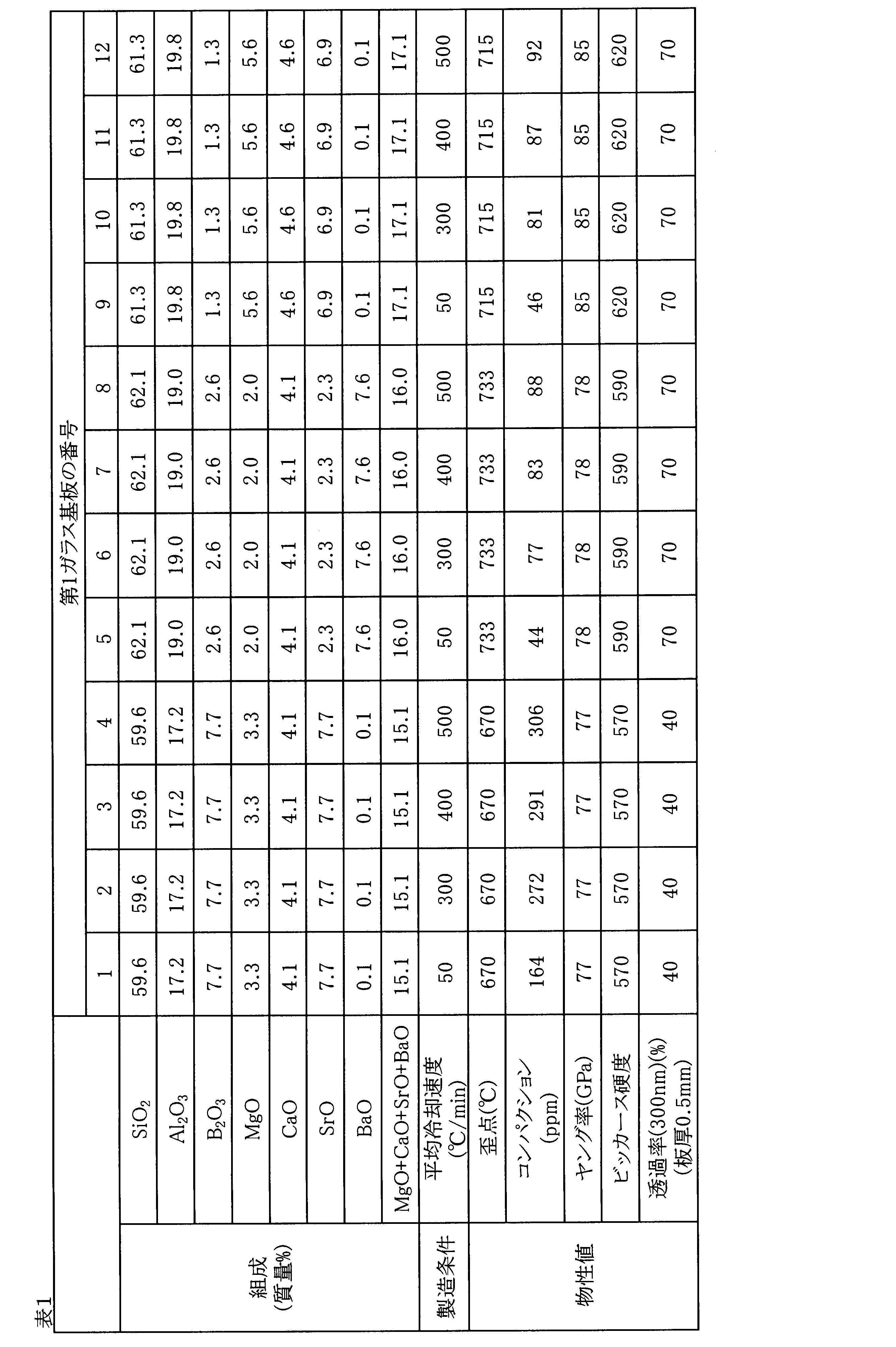
また、上記表中のコンパクションは100℃/時間で室温より昇温し、600℃で80分間の加熱処理を施し、100℃/時間で室温まで冷却した際のコンパクション(収縮率)を表す。これは、以下で述べる方法にて得られた計算値を示すが、上述した方法にて測定される実測値も上記表中の計算値とほぼ同じであった。
コンパクションCの計算は、ガラスの構造緩和を定式化した、以下の式を利用し、微小温度変化を与え、逐次計算することにより求めた。なお、各種パラメータ(β、τ)については、当該組成のガラスを用いて実測して得られたものを使用した。
(V(ξ)-V0)/(V∞―V0)=exp[-(ξ/τ)β]
C=106×ΔL/L=106×[1-(V(ξ)/V0)1/3]
ここで、V0は、処理時間0におけるガラスのモル体積、V∞は処理温度における平衡モル体積、V(ξ)は換算時間ξにおけるガラスのモル体積、Cはコンパクション(単位:ppm)、Lはガラスの長さ、ΔLはガラス長の処理前後における変化量、τは緩和時定数、βは緩和時定数の広がりを示すパラメータを示す。
表2は、表1のガラス基板に対して複数回(3回)の加熱処理を施してコンパクションを測定した結果を示す表である。第1ガラス基板1~12を用いて、以下の加熱条件による加熱処理を複数回実施した際の各加熱処理後におけるガラス基板のコンパクションを計算した。1回目欄は、以下の加熱処理を1回実施した後のガラス基板のコンパクション(ppm)を表す。2回目欄は、1回目の加熱処理をしたガラス基板を室温まで冷却してから、2回目の加熱処理を実施後のコンパクションを示す。3回目欄は、2回目の加熱処理をしたガラス基板を室温まで冷却してから、3回目の加熱処理を実施後のコンパクションを示す。
ガラス基板を室温から450℃まで5分間で昇温し、その後、450℃で20分間保持した後、室温となるまで5分間で冷却し、さらに、ガラス基板を室温から600℃まで5分間で昇温し、その後、600℃で5分間保持した後、室温となるまで5分間で冷却した。
アルケニル基含有オルガノポリシロキサン(数平均分子量:2000、アルケニル基の数:2個以上)(100質量部)と、ハイドロジェンポリシロキサン(数平均分子量:2000、ハイドロシリル基の数:2個以上)(6.7質量部)と配合した。なお、アルケニル基含有オルガノポリシロキサン中のアルケニル基と、ハイドロジェンポリシロキサン中のハイドロシリル基との混合モル比(ハイドロシリル基のモル数/アルケニル基のモル数)は0.4/1であった。さらに、触媒(白金触媒)を、アルケニル基含有オルガノポリシロキサンおよびハイドロジェンポリシロキサンの合計質量(100質量部)に対し、300ppm添加した。この液を、硬化性樹脂組成物Xとする。この硬化性樹脂組成物Xを、ダイコーターを用いて第1ガラス基板1の第1主面上に塗布して、未硬化のアルケニル基含有オルガノポリシロキサンおよびハイドロジェンポリシロキサンを含む層を第1ガラス基板1上に設けた。
その後、第2ガラス基板と、シリコーン樹脂層面とを、室温下で真空プレスにより貼り合わせ、ガラス積層体Aを得た。
この際、第2ガラス基板として、無アルカリホウケイ酸ガラスからなるガラス板(縦200mm、横200mm、板厚0.2mm、線膨張係数38×10―7/℃、旭硝子社製商品名「AN100」)を使用した。
得られたガラス積層体Aにおいては、第1ガラス基板と第2ガラス基板は、シリコーン樹脂層と気泡を発生することなく密着しており、歪み状欠点もなかった。また、ガラス積層体Aにおいて、シリコーン樹脂層と第1ガラス基板の層との界面の剥離強度は、第2ガラス基板の層とシリコーン樹脂層との界面の剥離強度よりも大きかった。
電子デバイスの製造方法としては、エキシマレーザアニール法を使用した、LTPSプロセスを使用した。まず、第2ガラス基板上に保護層を形成したのち、アモルファスシリコンを成膜した。脱水素工程、レーザー照射、活性化工程を行い、かつゲート電極、ソース、ドレイン電極等の各種配線を成膜、パターニングし、層間絶縁膜等の成膜を行い、薄膜トランジスタ回路を形成した。
なお、上記電子デバイスの製造工程において、製造プロセス温度が500℃以上の工程が含まれていた。
なお、シリコーン樹脂層は第1ガラス基板と共に第2ガラス基板から分離され、該結果より、第1ガラス基板の層とシリコーン樹脂層の界面の剥離強度(x)が、シリコーン樹脂層と第2ガラス基板の界面の剥離強度(y)よりも高いことが確認された。
この処理を2回繰り返して、電子デバイスの製造を行った。
なお、複数枚のガラス積層体Aを用意して、上記処理をそれぞれ実施した。
キャリア基板の2回目および3回目の使用時の電子デバイスの製造歩留まりが1回目と同等程度の場合は「A」、製造歩留まりが低下するが実用上許容範囲内である場合は「B」、製造歩留まりが大きく低下して実用上許容できない場合を「C」とした。

12,112 第1ガラス基板
14 密着層
16,116 基板
20 電子デバイス用部材
22 電子デバイス用部材付き積層体
24 部材付き基板(電子デバイス)
100,110 積層体
Claims (10)
- 基板の表面に電子デバイス用部材を製造する際に、前記基板に貼り合せられて用いられるキャリア基板であって、
前記キャリア基板は、少なくとも第1ガラス基板を含み、
前記第1ガラス基板は、下記コンパクションが80ppm以下である、キャリア基板。
コンパクション:前記第1ガラス基板を室温より100℃/時間で昇温し600℃で80分間の加熱処理をしてから、100℃/時間で室温まで冷却した場合の収縮率 - 前記コンパクションが70ppm以下である、請求項1に記載のキャリア基板。
- 前記第1ガラス基板の歪点が700℃以上である、請求項1または2に記載のキャリア基板。
- 前記第1ガラス基板が、酸化物基準の質量百分率表示において、下記を含有するガラスからなる、請求項1~3のいずれか1項に記載のキャリア基板。
SiO2:50~73%
Al2O3:10.5~24%
B2O3:0~5%
MgO:0~10%
CaO:0~14.5%
SrO:0~24%
BaO:0~13.5%
MgO+CaO+SrO+BaO:8~29.5% - さらに、前記第1ガラス基板上に配置された密着層を含む、請求項1~4のいずれか1項に記載のキャリア基板。
- 請求項1~5のいずれか1項に記載のキャリア基板と、前記キャリア基板上に配置された基板とを有する、積層体。
- 前記基板が第2ガラス基板である、請求項6に記載の積層体。
- 請求項6または7に記載の積層体の前記基板の表面上に電子デバイス用部材を形成し、電子デバイス用部材付き積層体を得る部材形成工程と、
前記電子デバイス用部材付き積層体から前記キャリア基板を除去し、前記基板と前記電子デバイス用部材とを有する電子デバイスを得る分離工程と、を備える電子デバイスの製造方法。 - 前記電子デバイス用部材が低温ポリシリコン(LTPS)を含む、請求項8に記載の電子デバイスの製造方法。
- 前記電子デバイス用部材を形成する際にプロセス温度が450℃以上である工程を含む、請求項9に記載の電子デバイスの製造方法。
Priority Applications (9)
| Application Number | Priority Date | Filing Date | Title |
|---|---|---|---|
| JP2017527403A JP6673354B2 (ja) | 2015-07-03 | 2016-06-28 | キャリア基板、積層体、電子デバイスの製造方法 |
| CN202210237147.7A CN114538771A (zh) | 2015-07-03 | 2016-06-28 | 载体基板、层叠体、电子器件的制造方法 |
| KR1020237044487A KR20240005182A (ko) | 2015-07-03 | 2016-06-28 | 캐리어 기판, 적층체, 전자 디바이스의 제조 방법 |
| KR1020267003855A KR20260028877A (ko) | 2015-07-03 | 2016-06-28 | 캐리어 기판, 적층체, 전자 디바이스의 제조 방법 |
| CN201680037288.7A CN107709258B (zh) | 2015-07-03 | 2016-06-28 | 载体基板、层叠体、电子器件的制造方法 |
| KR1020177035450A KR20180025859A (ko) | 2015-07-03 | 2016-06-28 | 캐리어 기판, 적층체, 전자 디바이스의 제조 방법 |
| US15/835,030 US11587958B2 (en) | 2015-07-03 | 2017-12-07 | Carrier substrate, laminate, and method for manufacturing electronic device |
| US18/066,497 US12581730B2 (en) | 2015-07-03 | 2022-12-15 | Carrier substrate, laminate, and method for manufacturing electronic device |
| US18/066,505 US20230118345A1 (en) | 2015-07-03 | 2022-12-15 | Carrier substrate, laminate, and method for manufacturing electronic device |
Applications Claiming Priority (2)
| Application Number | Priority Date | Filing Date | Title |
|---|---|---|---|
| JP2015-134697 | 2015-07-03 | ||
| JP2015134697 | 2015-07-03 |
Related Child Applications (1)
| Application Number | Title | Priority Date | Filing Date |
|---|---|---|---|
| US15/835,030 Continuation US11587958B2 (en) | 2015-07-03 | 2017-12-07 | Carrier substrate, laminate, and method for manufacturing electronic device |
Publications (1)
| Publication Number | Publication Date |
|---|---|
| WO2017006801A1 true WO2017006801A1 (ja) | 2017-01-12 |
Family
ID=57686160
Family Applications (1)
| Application Number | Title | Priority Date | Filing Date |
|---|---|---|---|
| PCT/JP2016/069080 Ceased WO2017006801A1 (ja) | 2015-07-03 | 2016-06-28 | キャリア基板、積層体、電子デバイスの製造方法 |
Country Status (6)
| Country | Link |
|---|---|
| US (3) | US11587958B2 (ja) |
| JP (1) | JP6673354B2 (ja) |
| KR (3) | KR20180025859A (ja) |
| CN (2) | CN114538771A (ja) |
| TW (2) | TWI695820B (ja) |
| WO (1) | WO2017006801A1 (ja) |
Cited By (6)
| Publication number | Priority date | Publication date | Assignee | Title |
|---|---|---|---|---|
| CN107644891A (zh) * | 2017-09-13 | 2018-01-30 | 武汉华星光电半导体显示技术有限公司 | 柔性oled面板的制作方法 |
| WO2018199059A1 (ja) * | 2017-04-27 | 2018-11-01 | 日本電気硝子株式会社 | キャリアガラス及びその製造方法 |
| WO2019021672A1 (ja) * | 2017-07-26 | 2019-01-31 | 日本電気硝子株式会社 | 支持ガラス基板及びこれを用いた積層基板 |
| KR20230088841A (ko) * | 2020-11-11 | 2023-06-20 | 어플라이드 머티어리얼스, 인코포레이티드 | 오존을 사용한 유리 캐리어 세정 |
| JP2024004095A (ja) * | 2022-06-28 | 2024-01-16 | Agc株式会社 | 積層体 |
| JP2024004253A (ja) * | 2022-06-28 | 2024-01-16 | Agc株式会社 | 積層体 |
Families Citing this family (5)
| Publication number | Priority date | Publication date | Assignee | Title |
|---|---|---|---|---|
| KR20180025859A (ko) * | 2015-07-03 | 2018-03-09 | 아사히 가라스 가부시키가이샤 | 캐리어 기판, 적층체, 전자 디바이스의 제조 방법 |
| CN109803825B (zh) * | 2016-10-07 | 2021-07-23 | 株式会社Lg化学 | 弯曲夹层玻璃及弯曲夹层玻璃的制造方法 |
| WO2019082357A1 (ja) * | 2017-10-26 | 2019-05-02 | 堺ディスプレイプロダクト株式会社 | フレキシブルoledデバイスの製造方法および製造装置 |
| TWI887301B (zh) * | 2019-11-21 | 2025-06-21 | 美商康寧公司 | 回收玻璃及玻璃陶瓷載體基板 |
| KR102893085B1 (ko) * | 2022-11-11 | 2025-12-04 | 주식회사 영민 | 대전 방지용 전도성 pfa 및 대전 방지용 전도성 pfa 제품의 제조 방법 |
Citations (5)
| Publication number | Priority date | Publication date | Assignee | Title |
|---|---|---|---|---|
| JP2011020864A (ja) * | 2009-07-13 | 2011-02-03 | Nippon Electric Glass Co Ltd | ガラス基板の製造方法 |
| WO2011024775A1 (ja) * | 2009-08-28 | 2011-03-03 | 荒川化学工業株式会社 | 支持体、ガラス基板積層体、支持体付き表示装置用パネル、および表示装置用パネルの製造方法 |
| JP2012086527A (ja) * | 2010-10-22 | 2012-05-10 | Asahi Glass Co Ltd | 支持体、ガラス基板積層体、支持体付き表示装置用パネル、オルガノポリシロキサン組成物、および表示装置用パネルの製造方法 |
| JP2014043356A (ja) * | 2012-08-24 | 2014-03-13 | Nippon Electric Glass Co Ltd | ガラス板の製造方法及びガラス板の製造装置 |
| WO2016111152A1 (ja) * | 2015-01-05 | 2016-07-14 | 日本電気硝子株式会社 | 支持ガラス基板及びその製造方法 |
Family Cites Families (21)
| Publication number | Priority date | Publication date | Assignee | Title |
|---|---|---|---|---|
| US3338696A (en) | 1964-05-06 | 1967-08-29 | Corning Glass Works | Sheet forming apparatus |
| BE757057A (fr) | 1969-10-06 | 1971-04-05 | Corning Glass Works | Procede et appareil de controle d'epaisseur d'une feuille de verre nouvellement etiree |
| US5597395A (en) * | 1995-11-28 | 1997-01-28 | Corning Incorporated | Method for low temperature precompaction of glass |
| JP5200538B2 (ja) | 2005-08-09 | 2013-06-05 | 旭硝子株式会社 | 薄板ガラス積層体及び薄板ガラス積層体を用いた表示装置の製造方法 |
| US7833919B2 (en) * | 2006-02-10 | 2010-11-16 | Corning Incorporated | Glass compositions having high thermal and chemical stability and methods of making thereof |
| US8713967B2 (en) * | 2008-11-21 | 2014-05-06 | Corning Incorporated | Stable glass sheet and method for making same |
| US20110265516A1 (en) * | 2010-04-29 | 2011-11-03 | Douglas Clippinger Allan | Compositional control of fast relaxation in display glasses |
| WO2012137780A1 (ja) * | 2011-04-08 | 2012-10-11 | 旭硝子株式会社 | 基板用無アルカリガラスおよび基板用無アルカリガラスの製造方法 |
| JP5887946B2 (ja) | 2012-01-18 | 2016-03-16 | 旭硝子株式会社 | 電子デバイスの製造方法、およびガラス積層体の製造方法 |
| KR20150029633A (ko) * | 2012-06-05 | 2015-03-18 | 아사히 가라스 가부시키가이샤 | 무알칼리 유리 및 그 제조 방법 |
| WO2014087971A1 (ja) * | 2012-12-05 | 2014-06-12 | 旭硝子株式会社 | 無アルカリガラス基板 |
| US9340443B2 (en) * | 2012-12-13 | 2016-05-17 | Corning Incorporated | Bulk annealing of glass sheets |
| US9051206B2 (en) * | 2012-12-21 | 2015-06-09 | Corning Incorporated | Glass with improved total pitch stability |
| JP2016153346A (ja) * | 2013-06-27 | 2016-08-25 | 旭硝子株式会社 | 無アルカリガラス |
| JP2016153345A (ja) * | 2013-06-27 | 2016-08-25 | 旭硝子株式会社 | 無アルカリガラス |
| KR20250048598A (ko) * | 2014-10-23 | 2025-04-09 | 에이지씨 가부시키가이샤 | 무알칼리 유리 |
| KR20180025859A (ko) * | 2015-07-03 | 2018-03-09 | 아사히 가라스 가부시키가이샤 | 캐리어 기판, 적층체, 전자 디바이스의 제조 방법 |
| JP6315011B2 (ja) * | 2016-03-15 | 2018-04-25 | 旭硝子株式会社 | 無アルカリガラス基板、および無アルカリガラス基板の製造方法 |
| JP7110981B2 (ja) * | 2016-08-05 | 2022-08-02 | Agc株式会社 | ガラス基板、半導体装置および表示装置 |
| CN115557695B (zh) * | 2016-08-23 | 2024-10-29 | Agc株式会社 | 无碱玻璃 |
| KR102680019B1 (ko) * | 2018-03-14 | 2024-07-02 | 에이지씨 가부시키가이샤 | 무알칼리 유리 |
-
2016
- 2016-06-28 KR KR1020177035450A patent/KR20180025859A/ko not_active Ceased
- 2016-06-28 CN CN202210237147.7A patent/CN114538771A/zh active Pending
- 2016-06-28 KR KR1020267003855A patent/KR20260028877A/ko active Pending
- 2016-06-28 WO PCT/JP2016/069080 patent/WO2017006801A1/ja not_active Ceased
- 2016-06-28 JP JP2017527403A patent/JP6673354B2/ja active Active
- 2016-06-28 KR KR1020237044487A patent/KR20240005182A/ko not_active Ceased
- 2016-06-28 CN CN201680037288.7A patent/CN107709258B/zh active Active
- 2016-06-29 TW TW105120619A patent/TWI695820B/zh active
- 2016-06-29 TW TW109104880A patent/TWI720817B/zh active
-
2017
- 2017-12-07 US US15/835,030 patent/US11587958B2/en active Active
-
2022
- 2022-12-15 US US18/066,497 patent/US12581730B2/en active Active
- 2022-12-15 US US18/066,505 patent/US20230118345A1/en not_active Abandoned
Patent Citations (5)
| Publication number | Priority date | Publication date | Assignee | Title |
|---|---|---|---|---|
| JP2011020864A (ja) * | 2009-07-13 | 2011-02-03 | Nippon Electric Glass Co Ltd | ガラス基板の製造方法 |
| WO2011024775A1 (ja) * | 2009-08-28 | 2011-03-03 | 荒川化学工業株式会社 | 支持体、ガラス基板積層体、支持体付き表示装置用パネル、および表示装置用パネルの製造方法 |
| JP2012086527A (ja) * | 2010-10-22 | 2012-05-10 | Asahi Glass Co Ltd | 支持体、ガラス基板積層体、支持体付き表示装置用パネル、オルガノポリシロキサン組成物、および表示装置用パネルの製造方法 |
| JP2014043356A (ja) * | 2012-08-24 | 2014-03-13 | Nippon Electric Glass Co Ltd | ガラス板の製造方法及びガラス板の製造装置 |
| WO2016111152A1 (ja) * | 2015-01-05 | 2016-07-14 | 日本電気硝子株式会社 | 支持ガラス基板及びその製造方法 |
Cited By (18)
| Publication number | Priority date | Publication date | Assignee | Title |
|---|---|---|---|---|
| JP7172996B2 (ja) | 2017-04-27 | 2022-11-16 | 日本電気硝子株式会社 | キャリアガラス及びその製造方法 |
| JP2023011770A (ja) * | 2017-04-27 | 2023-01-24 | 日本電気硝子株式会社 | キャリアガラス及びその製造方法 |
| US12109780B2 (en) | 2017-04-27 | 2024-10-08 | Nippon Electric Glass Co., Ltd. | Carrier glass and method for producing same |
| KR102706630B1 (ko) * | 2017-04-27 | 2024-09-13 | 니폰 덴키 가라스 가부시키가이샤 | 캐리어 유리 및 그 제조 방법 |
| CN110603234A (zh) * | 2017-04-27 | 2019-12-20 | 日本电气硝子株式会社 | 载体玻璃及其制造方法 |
| KR20190141654A (ko) * | 2017-04-27 | 2019-12-24 | 니폰 덴키 가라스 가부시키가이샤 | 캐리어 유리 및 그 제조 방법 |
| JP7392916B2 (ja) | 2017-04-27 | 2023-12-06 | 日本電気硝子株式会社 | キャリアガラス及びその製造方法 |
| JPWO2018199059A1 (ja) * | 2017-04-27 | 2020-03-12 | 日本電気硝子株式会社 | キャリアガラス及びその製造方法 |
| WO2018199059A1 (ja) * | 2017-04-27 | 2018-11-01 | 日本電気硝子株式会社 | キャリアガラス及びその製造方法 |
| CN115366504A (zh) * | 2017-04-27 | 2022-11-22 | 日本电气硝子株式会社 | 载体玻璃及其制造方法 |
| CN110831908A (zh) * | 2017-07-26 | 2020-02-21 | 日本电气硝子株式会社 | 支承玻璃基板和使用了其的层叠基板 |
| WO2019021672A1 (ja) * | 2017-07-26 | 2019-01-31 | 日本電気硝子株式会社 | 支持ガラス基板及びこれを用いた積層基板 |
| CN107644891A (zh) * | 2017-09-13 | 2018-01-30 | 武汉华星光电半导体显示技术有限公司 | 柔性oled面板的制作方法 |
| WO2019051940A1 (zh) * | 2017-09-13 | 2019-03-21 | 武汉华星光电半导体显示技术有限公司 | 柔性oled面板的制作方法 |
| KR20230088841A (ko) * | 2020-11-11 | 2023-06-20 | 어플라이드 머티어리얼스, 인코포레이티드 | 오존을 사용한 유리 캐리어 세정 |
| KR102648258B1 (ko) * | 2020-11-11 | 2024-03-14 | 어플라이드 머티어리얼스, 인코포레이티드 | 오존을 사용한 유리 캐리어 세정 |
| JP2024004095A (ja) * | 2022-06-28 | 2024-01-16 | Agc株式会社 | 積層体 |
| JP2024004253A (ja) * | 2022-06-28 | 2024-01-16 | Agc株式会社 | 積層体 |
Also Published As
| Publication number | Publication date |
|---|---|
| KR20260028877A (ko) | 2026-03-04 |
| CN107709258A (zh) | 2018-02-16 |
| US11587958B2 (en) | 2023-02-21 |
| US20180122838A1 (en) | 2018-05-03 |
| TWI720817B (zh) | 2021-03-01 |
| JPWO2017006801A1 (ja) | 2018-04-19 |
| US12581730B2 (en) | 2026-03-17 |
| US20230154938A1 (en) | 2023-05-18 |
| KR20180025859A (ko) | 2018-03-09 |
| TWI695820B (zh) | 2020-06-11 |
| KR20240005182A (ko) | 2024-01-11 |
| TW202023983A (zh) | 2020-07-01 |
| JP6673354B2 (ja) | 2020-03-25 |
| TW201708144A (zh) | 2017-03-01 |
| CN114538771A (zh) | 2022-05-27 |
| US20230118345A1 (en) | 2023-04-20 |
| CN107709258B (zh) | 2022-04-01 |
Similar Documents
| Publication | Publication Date | Title |
|---|---|---|
| US12581730B2 (en) | Carrier substrate, laminate, and method for manufacturing electronic device | |
| JP7136275B2 (ja) | 積層体、電子デバイスの製造方法、積層体の製造方法 | |
| JP6176067B2 (ja) | ガラス積層体および電子デバイスの製造方法 | |
| JP6119567B2 (ja) | ガラス積層体の製造方法および電子デバイスの製造方法 | |
| WO2012144499A1 (ja) | 積層体、その製造方法及び用途 | |
| JPWO2015163134A1 (ja) | ガラス積層体および電子デバイスの製造方法 | |
| CN104903095B (zh) | 玻璃层叠体及其制造方法、以及带有机硅树脂层的支撑基材 | |
| KR102526047B1 (ko) | 유리 적층체 및 그의 제조 방법 | |
| KR102475698B1 (ko) | 적층 기판 및 전자 디바이스의 제조 방법 | |
| CN105128460A (zh) | 带树脂层的支撑基板及其制造方法、玻璃层叠体、以及电子设备的制造方法 | |
| JP2017164903A (ja) | ガラス積層体、無機層付き支持基板、電子デバイスの製造方法、無機層付き支持基板の製造方法 | |
| WO2016017649A1 (ja) | ガラス積層体、無機層付き支持基板、電子デバイスの製造方法及び、無機層付き支持基板の製造方法 | |
| CN106142762A (zh) | 玻璃层叠体及电子器件的制造方法 |
Legal Events
| Date | Code | Title | Description |
|---|---|---|---|
| 121 | Ep: the epo has been informed by wipo that ep was designated in this application |
Ref document number: 16821270 Country of ref document: EP Kind code of ref document: A1 |
|
| ENP | Entry into the national phase |
Ref document number: 20177035450 Country of ref document: KR Kind code of ref document: A |
|
| ENP | Entry into the national phase |
Ref document number: 2017527403 Country of ref document: JP Kind code of ref document: A |
|
| NENP | Non-entry into the national phase |
Ref country code: DE |
|
| 122 | Ep: pct application non-entry in european phase |
Ref document number: 16821270 Country of ref document: EP Kind code of ref document: A1 |
|
| WWR | Wipo information: refused in national office |
Ref document number: 1020237044487 Country of ref document: KR |
|
| WWC | Wipo information: continuation of processing after refusal or withdrawal |
Ref document number: 1020237044487 Country of ref document: KR |
|
| WWD | Wipo information: divisional of initial pct application |
Ref document number: 1020267003855 Country of ref document: KR |
|
| WWP | Wipo information: published in national office |
Ref document number: 1020267003855 Country of ref document: KR |