WO2016208553A1 - 半導体デバイス電極の製造方法 - Google Patents
半導体デバイス電極の製造方法 Download PDFInfo
- Publication number
- WO2016208553A1 WO2016208553A1 PCT/JP2016/068327 JP2016068327W WO2016208553A1 WO 2016208553 A1 WO2016208553 A1 WO 2016208553A1 JP 2016068327 W JP2016068327 W JP 2016068327W WO 2016208553 A1 WO2016208553 A1 WO 2016208553A1
- Authority
- WO
- WIPO (PCT)
- Prior art keywords
- metal
- thin film
- silicide
- semiconductor device
- electrode
- Prior art date
- Legal status (The legal status is an assumption and is not a legal conclusion. Google has not performed a legal analysis and makes no representation as to the accuracy of the status listed.)
- Ceased
Links
Images


Classifications
-
- H—ELECTRICITY
- H10—SEMICONDUCTOR DEVICES; ELECTRIC SOLID-STATE DEVICES NOT OTHERWISE PROVIDED FOR
- H10D—INORGANIC ELECTRIC SEMICONDUCTOR DEVICES
- H10D64/00—Electrodes of devices having potential barriers
- H10D64/01—Manufacture or treatment
- H10D64/011—Manufacture or treatment of electrodes ohmically coupled to a semiconductor
- H10D64/0111—Manufacture or treatment of electrodes ohmically coupled to a semiconductor to Group IV semiconductors
- H10D64/0112—Manufacture or treatment of electrodes ohmically coupled to a semiconductor to Group IV semiconductors using conductive layers comprising silicides
-
- H—ELECTRICITY
- H10—SEMICONDUCTOR DEVICES; ELECTRIC SOLID-STATE DEVICES NOT OTHERWISE PROVIDED FOR
- H10D—INORGANIC ELECTRIC SEMICONDUCTOR DEVICES
- H10D64/00—Electrodes of devices having potential barriers
- H10D64/01—Manufacture or treatment
- H10D64/011—Manufacture or treatment of electrodes ohmically coupled to a semiconductor
-
- C—CHEMISTRY; METALLURGY
- C23—COATING METALLIC MATERIAL; COATING MATERIAL WITH METALLIC MATERIAL; CHEMICAL SURFACE TREATMENT; DIFFUSION TREATMENT OF METALLIC MATERIAL; COATING BY VACUUM EVAPORATION, BY SPUTTERING, BY ION IMPLANTATION OR BY CHEMICAL VAPOUR DEPOSITION, IN GENERAL; INHIBITING CORROSION OF METALLIC MATERIAL OR INCRUSTATION IN GENERAL
- C23C—COATING METALLIC MATERIAL; COATING MATERIAL WITH METALLIC MATERIAL; SURFACE TREATMENT OF METALLIC MATERIAL BY DIFFUSION INTO THE SURFACE, BY CHEMICAL CONVERSION OR SUBSTITUTION; COATING BY VACUUM EVAPORATION, BY SPUTTERING, BY ION IMPLANTATION OR BY CHEMICAL VAPOUR DEPOSITION, IN GENERAL
- C23C14/00—Coating by vacuum evaporation, by sputtering or by ion implantation of the coating forming material
- C23C14/0021—Reactive sputtering or evaporation
- C23C14/0036—Reactive sputtering
-
- C—CHEMISTRY; METALLURGY
- C23—COATING METALLIC MATERIAL; COATING MATERIAL WITH METALLIC MATERIAL; CHEMICAL SURFACE TREATMENT; DIFFUSION TREATMENT OF METALLIC MATERIAL; COATING BY VACUUM EVAPORATION, BY SPUTTERING, BY ION IMPLANTATION OR BY CHEMICAL VAPOUR DEPOSITION, IN GENERAL; INHIBITING CORROSION OF METALLIC MATERIAL OR INCRUSTATION IN GENERAL
- C23C—COATING METALLIC MATERIAL; COATING MATERIAL WITH METALLIC MATERIAL; SURFACE TREATMENT OF METALLIC MATERIAL BY DIFFUSION INTO THE SURFACE, BY CHEMICAL CONVERSION OR SUBSTITUTION; COATING BY VACUUM EVAPORATION, BY SPUTTERING, BY ION IMPLANTATION OR BY CHEMICAL VAPOUR DEPOSITION, IN GENERAL
- C23C14/00—Coating by vacuum evaporation, by sputtering or by ion implantation of the coating forming material
- C23C14/06—Coating by vacuum evaporation, by sputtering or by ion implantation of the coating forming material characterised by the coating material
-
- C—CHEMISTRY; METALLURGY
- C23—COATING METALLIC MATERIAL; COATING MATERIAL WITH METALLIC MATERIAL; CHEMICAL SURFACE TREATMENT; DIFFUSION TREATMENT OF METALLIC MATERIAL; COATING BY VACUUM EVAPORATION, BY SPUTTERING, BY ION IMPLANTATION OR BY CHEMICAL VAPOUR DEPOSITION, IN GENERAL; INHIBITING CORROSION OF METALLIC MATERIAL OR INCRUSTATION IN GENERAL
- C23C—COATING METALLIC MATERIAL; COATING MATERIAL WITH METALLIC MATERIAL; SURFACE TREATMENT OF METALLIC MATERIAL BY DIFFUSION INTO THE SURFACE, BY CHEMICAL CONVERSION OR SUBSTITUTION; COATING BY VACUUM EVAPORATION, BY SPUTTERING, BY ION IMPLANTATION OR BY CHEMICAL VAPOUR DEPOSITION, IN GENERAL
- C23C14/00—Coating by vacuum evaporation, by sputtering or by ion implantation of the coating forming material
- C23C14/06—Coating by vacuum evaporation, by sputtering or by ion implantation of the coating forming material characterised by the coating material
- C23C14/0641—Nitrides
-
- C—CHEMISTRY; METALLURGY
- C23—COATING METALLIC MATERIAL; COATING MATERIAL WITH METALLIC MATERIAL; CHEMICAL SURFACE TREATMENT; DIFFUSION TREATMENT OF METALLIC MATERIAL; COATING BY VACUUM EVAPORATION, BY SPUTTERING, BY ION IMPLANTATION OR BY CHEMICAL VAPOUR DEPOSITION, IN GENERAL; INHIBITING CORROSION OF METALLIC MATERIAL OR INCRUSTATION IN GENERAL
- C23C—COATING METALLIC MATERIAL; COATING MATERIAL WITH METALLIC MATERIAL; SURFACE TREATMENT OF METALLIC MATERIAL BY DIFFUSION INTO THE SURFACE, BY CHEMICAL CONVERSION OR SUBSTITUTION; COATING BY VACUUM EVAPORATION, BY SPUTTERING, BY ION IMPLANTATION OR BY CHEMICAL VAPOUR DEPOSITION, IN GENERAL
- C23C14/00—Coating by vacuum evaporation, by sputtering or by ion implantation of the coating forming material
- C23C14/06—Coating by vacuum evaporation, by sputtering or by ion implantation of the coating forming material characterised by the coating material
- C23C14/14—Metallic material, boron or silicon
-
- C—CHEMISTRY; METALLURGY
- C23—COATING METALLIC MATERIAL; COATING MATERIAL WITH METALLIC MATERIAL; CHEMICAL SURFACE TREATMENT; DIFFUSION TREATMENT OF METALLIC MATERIAL; COATING BY VACUUM EVAPORATION, BY SPUTTERING, BY ION IMPLANTATION OR BY CHEMICAL VAPOUR DEPOSITION, IN GENERAL; INHIBITING CORROSION OF METALLIC MATERIAL OR INCRUSTATION IN GENERAL
- C23C—COATING METALLIC MATERIAL; COATING MATERIAL WITH METALLIC MATERIAL; SURFACE TREATMENT OF METALLIC MATERIAL BY DIFFUSION INTO THE SURFACE, BY CHEMICAL CONVERSION OR SUBSTITUTION; COATING BY VACUUM EVAPORATION, BY SPUTTERING, BY ION IMPLANTATION OR BY CHEMICAL VAPOUR DEPOSITION, IN GENERAL
- C23C14/00—Coating by vacuum evaporation, by sputtering or by ion implantation of the coating forming material
- C23C14/06—Coating by vacuum evaporation, by sputtering or by ion implantation of the coating forming material characterised by the coating material
- C23C14/14—Metallic material, boron or silicon
- C23C14/16—Metallic material, boron or silicon on metallic substrates or on substrates of boron or silicon
- C23C14/165—Metallic material, boron or silicon on metallic substrates or on substrates of boron or silicon by cathodic sputtering
-
- C—CHEMISTRY; METALLURGY
- C23—COATING METALLIC MATERIAL; COATING MATERIAL WITH METALLIC MATERIAL; CHEMICAL SURFACE TREATMENT; DIFFUSION TREATMENT OF METALLIC MATERIAL; COATING BY VACUUM EVAPORATION, BY SPUTTERING, BY ION IMPLANTATION OR BY CHEMICAL VAPOUR DEPOSITION, IN GENERAL; INHIBITING CORROSION OF METALLIC MATERIAL OR INCRUSTATION IN GENERAL
- C23C—COATING METALLIC MATERIAL; COATING MATERIAL WITH METALLIC MATERIAL; SURFACE TREATMENT OF METALLIC MATERIAL BY DIFFUSION INTO THE SURFACE, BY CHEMICAL CONVERSION OR SUBSTITUTION; COATING BY VACUUM EVAPORATION, BY SPUTTERING, BY ION IMPLANTATION OR BY CHEMICAL VAPOUR DEPOSITION, IN GENERAL
- C23C14/00—Coating by vacuum evaporation, by sputtering or by ion implantation of the coating forming material
- C23C14/58—After-treatment
-
- C—CHEMISTRY; METALLURGY
- C23—COATING METALLIC MATERIAL; COATING MATERIAL WITH METALLIC MATERIAL; CHEMICAL SURFACE TREATMENT; DIFFUSION TREATMENT OF METALLIC MATERIAL; COATING BY VACUUM EVAPORATION, BY SPUTTERING, BY ION IMPLANTATION OR BY CHEMICAL VAPOUR DEPOSITION, IN GENERAL; INHIBITING CORROSION OF METALLIC MATERIAL OR INCRUSTATION IN GENERAL
- C23C—COATING METALLIC MATERIAL; COATING MATERIAL WITH METALLIC MATERIAL; SURFACE TREATMENT OF METALLIC MATERIAL BY DIFFUSION INTO THE SURFACE, BY CHEMICAL CONVERSION OR SUBSTITUTION; COATING BY VACUUM EVAPORATION, BY SPUTTERING, BY ION IMPLANTATION OR BY CHEMICAL VAPOUR DEPOSITION, IN GENERAL
- C23C14/00—Coating by vacuum evaporation, by sputtering or by ion implantation of the coating forming material
- C23C14/58—After-treatment
- C23C14/5873—Removal of material
-
- H—ELECTRICITY
- H10—SEMICONDUCTOR DEVICES; ELECTRIC SOLID-STATE DEVICES NOT OTHERWISE PROVIDED FOR
- H10D—INORGANIC ELECTRIC SEMICONDUCTOR DEVICES
- H10D62/00—Semiconductor bodies, or regions thereof, of devices having potential barriers
- H10D62/80—Semiconductor bodies, or regions thereof, of devices having potential barriers characterised by the materials
- H10D62/83—Semiconductor bodies, or regions thereof, of devices having potential barriers characterised by the materials being Group IV materials, e.g. B-doped Si or undoped Ge
-
- H—ELECTRICITY
- H10—SEMICONDUCTOR DEVICES; ELECTRIC SOLID-STATE DEVICES NOT OTHERWISE PROVIDED FOR
- H10D—INORGANIC ELECTRIC SEMICONDUCTOR DEVICES
- H10D64/00—Electrodes of devices having potential barriers
- H10D64/01—Manufacture or treatment
-
- H—ELECTRICITY
- H10—SEMICONDUCTOR DEVICES; ELECTRIC SOLID-STATE DEVICES NOT OTHERWISE PROVIDED FOR
- H10D—INORGANIC ELECTRIC SEMICONDUCTOR DEVICES
- H10D64/00—Electrodes of devices having potential barriers
- H10D64/20—Electrodes characterised by their shapes, relative sizes or dispositions
- H10D64/23—Electrodes carrying the current to be rectified, amplified, oscillated or switched, e.g. sources, drains, anodes or cathodes
- H10D64/251—Source or drain electrodes for field-effect devices
-
- H—ELECTRICITY
- H10—SEMICONDUCTOR DEVICES; ELECTRIC SOLID-STATE DEVICES NOT OTHERWISE PROVIDED FOR
- H10D—INORGANIC ELECTRIC SEMICONDUCTOR DEVICES
- H10D64/00—Electrodes of devices having potential barriers
- H10D64/60—Electrodes characterised by their materials
- H10D64/62—Electrodes ohmically coupled to a semiconductor
-
- H—ELECTRICITY
- H10—SEMICONDUCTOR DEVICES; ELECTRIC SOLID-STATE DEVICES NOT OTHERWISE PROVIDED FOR
- H10P—GENERIC PROCESSES OR APPARATUS FOR THE MANUFACTURE OR TREATMENT OF DEVICES COVERED BY CLASS H10
- H10P14/00—Formation of materials, e.g. in the shape of layers or pillars
- H10P14/40—Formation of materials, e.g. in the shape of layers or pillars of conductive or resistive materials
- H10P14/42—Formation of materials, e.g. in the shape of layers or pillars of conductive or resistive materials using a gas or vapour
- H10P14/44—Physical vapour deposition [PVD]
-
- H—ELECTRICITY
- H10—SEMICONDUCTOR DEVICES; ELECTRIC SOLID-STATE DEVICES NOT OTHERWISE PROVIDED FOR
- H10P—GENERIC PROCESSES OR APPARATUS FOR THE MANUFACTURE OR TREATMENT OF DEVICES COVERED BY CLASS H10
- H10P14/00—Formation of materials, e.g. in the shape of layers or pillars
- H10P14/60—Formation of materials, e.g. in the shape of layers or pillars of insulating materials
- H10P14/69—Inorganic materials
- H10P14/692—Inorganic materials composed of oxides, glassy oxides or oxide-based glasses
- H10P14/6938—Inorganic materials composed of oxides, glassy oxides or oxide-based glasses the material containing at least one metal element, e.g. metal oxides, metal oxynitrides or metal oxycarbides
- H10P14/6939—Inorganic materials composed of oxides, glassy oxides or oxide-based glasses the material containing at least one metal element, e.g. metal oxides, metal oxynitrides or metal oxycarbides characterised by the metal
- H10P14/69392—Inorganic materials composed of oxides, glassy oxides or oxide-based glasses the material containing at least one metal element, e.g. metal oxides, metal oxynitrides or metal oxycarbides characterised by the metal the material containing hafnium, e.g. HfO2
-
- H—ELECTRICITY
- H10—SEMICONDUCTOR DEVICES; ELECTRIC SOLID-STATE DEVICES NOT OTHERWISE PROVIDED FOR
- H10P—GENERIC PROCESSES OR APPARATUS FOR THE MANUFACTURE OR TREATMENT OF DEVICES COVERED BY CLASS H10
- H10P95/00—Generic processes or apparatus for manufacture or treatments not covered by the other groups of this subclass
- H10P95/90—Thermal treatments, e.g. annealing or sintering
-
- H—ELECTRICITY
- H10—SEMICONDUCTOR DEVICES; ELECTRIC SOLID-STATE DEVICES NOT OTHERWISE PROVIDED FOR
- H10W—GENERIC PACKAGES, INTERCONNECTIONS, CONNECTORS OR OTHER CONSTRUCTIONAL DETAILS OF DEVICES COVERED BY CLASS H10
- H10W20/00—Interconnections in chips, wafers or substrates
- H10W20/01—Manufacture or treatment
- H10W20/031—Manufacture or treatment of conductive parts of the interconnections
- H10W20/064—Manufacture or treatment of conductive parts of the interconnections by modifying the conductivity of conductive parts, e.g. by alloying
- H10W20/066—Manufacture or treatment of conductive parts of the interconnections by modifying the conductivity of conductive parts, e.g. by alloying by forming silicides of refractory metals
Definitions
- the present invention relates to a method for manufacturing a silicide electrode in a semiconductor device such as a MOSFET.
- a gate electrode and a source / drain region are formed on a silicon substrate, and then a silicide electrode is formed in the source / drain region in order to form a metal / semiconductor junction.
- the silicide electrode is formed by depositing a metal thin film on the substrate by sputtering or the like and then heat-treating it to diffuse silicon into the metal thin film and silicidize.
- titanium silicide (TiSi 2 ) and cobalt silicide (CoSi 2 ) are generally known in the past.
- NiSi nickel silicide
- platinum silicide (PtSi) that does not cause a phase transition in the heat treatment during silicidation is also expected.
- a metal thin film of silicide such as Ni and heat-treat it.
- this heat processing temperature is based also on a metal, it is about 300 degreeC or more and about 600 degreeC. Therefore, there is a concern about the formation of an insulating film due to oxidation of the metal as silicidation progresses in the heat treatment process.
- the surface form of the silicide electrode may be deteriorated due to oxidation of the metal, which may increase the electrical resistance.
- the second metal compound film may be referred to as a Cap layer (cap layer)).
- TiN titanium nitride
- TiC titanium carbide
- the present invention has been made based on the above background, and relates to a method of forming a silicide electrode on a silicon substrate.
- the present invention relates to the formation of an insulating film by oxidation of a first metal thin film formed during silicidation. Provided is one that can more effectively suppress changes in surface morphology.
- the present inventors examined the constituent material of the Cap layer for protecting the first metal in order to solve the above problems. As a result, the present inventors have conceived the present invention that hafnium (Hf) is particularly effective as the second metal.
- the present invention provides a step of forming a first thin film made of a first metal on a substrate containing Si, and a second thin film made of a compound of a second metal on the first thin film.
- a semiconductor device electrode comprising: a step of forming; and a step of forming a first metal silicide electrode by heat treatment, wherein the second metal is applied with hafnium (Hf).
- Hf hafnium
- the first metal thin film for manufacturing the silicide electrode is formed on the Si portion of the substrate.
- a Si substrate is usually used as a device substrate, and a source / drain is formed. Therefore, a diffusion layer is formed by doping a corresponding region with a dopant.
- the first thin film is formed on this source / drain region.
- the diffusion layer is formed by a conventional general method.
- the gate electrode is also formed in accordance with the prior art.
- the first metal constituting the silicide electrode is preferably Ti, Co, Ni, Pt or an alloy thereof.
- consideration is given to the versatility of Ti silicide and Co silicide, Ni silicide characteristics for extremely reducing the junction depth, and the good heat resistance of Pt silicide.
- the silicide of an alloy of Pt and Hf (PtHf) also has a work function near midgap with respect to Si (n-Si or p-Si) constituting the substrate, and is useful from the viewpoint that the barrier height can be reduced. This is a silicide electrode.
- the film thickness of the first thin film is determined by the junction depth required for the device and is not related to the suppression of oxidation of the first metal, which is the subject matter of the present invention. Therefore, the thickness of the first thin film is not limited by the present application.
- the method for forming the first metal thin film is not particularly limited, and any of a physical method such as a sputtering method and a vacuum evaporation method and a chemical method such as a chemical vapor deposition method (CVD method) can be applied.
- the sputtering method is preferable.
- the thin film is formed by magnetron sputtering, ion beam sputtering, electron cyclotron resonance (ECR) sputtering, mirrortron sputtering, radio frequency (RF) sputtering, direct current (DC) sputtering, or the like.
- Hf is applied as the second metal.
- Hf has a characteristic that it is relatively easy to develop and maintain an amorphous phase during compound formation, and structural changes due to crystallization hardly occur even when heated. . Therefore, when compared with TiN or the like conventionally used as a Cap layer, the Hf compound has high heat resistance and excellent barrier performance against the first thin film.
- HfN As specific examples of Hf compounds, HfN, HfW, HfB, and the like can be applied. Among these Hf compounds, HfN is more preferable because it can form a film having high amorphous phase and high heat resistance. In addition, HfN has good etching properties and has an advantage that the removal process after silicidation can be simplified.
- the thickness of the Hf compound thin film is preferably 10 nm or more and 20 nm or less. This is because the film has high oxidation resistance and is difficult to crystallize.
- the method for forming the Hf compound thin film is not particularly limited as in the case of the first thin film, but the sputtering method is preferred. Reactive sputtering is applied to form a nitride film.
- the first metal is silicided by heat treatment (annealing).
- This heat treatment is preferably performed at 400 ° C. or higher and 600 ° C. or lower. This is because the heat treatment temperature can reduce the resistivity.
- the heat treatment atmosphere is preferably a non-oxidizing atmosphere (vacuum atmosphere, inert gas atmosphere, reducing atmosphere).
- the heat treatment is preferably performed using a rapid heat treatment apparatus.
- the Hf compound thin film which is the second thin film, serves to barrier the first metal during silicidation by annealing, and thus completes its role upon completion of annealing.
- the removal of the Hf compound thin film is preferably by wet etching.
- Preferred etching solutions include dilute hydrofluoric acid and buffered hydrofluoric acid.
- the etching solution is selected according to the type of the first metal, and examples thereof include dilute hydrofluoric acid, aqua regia, and sulfuric acid.
- the first metal silicide electrode is formed on the substrate.
- the subsequent steps follow conventional processes.
- the present invention optimizes the constituent material of the second metal compound (Cap layer) that suppresses the oxidation of the first metal thin film to be silicided when manufacturing the silicide electrode of the semiconductor device.
- the Hf compound applied in the present invention has a barrier performance superior to that of the prior art, and can cope with the manufacture of a miniaturized / thinned silicide film.
- First Embodiment As a preliminary test, Pt is formed as a first metal to form Pt silicide on an Si substrate, and a case where a HfN thin film is formed thereon and not formed is used. The surface morphology of the silicide electrode after annealing was examined.
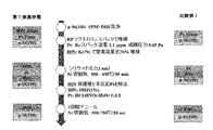
- FIG. 1 shows a comparative test process according to this embodiment.
- a Si substrate p-Si (100)
- a Pt thin film was formed to a thickness of 10 nm by sputtering.
- the HfN thin film was formed on the Pt thin film.
- the HfN thin film was formed by reactive sputtering using a Hf target and setting the film formation atmosphere to Kr / N 2 (film thickness 20 nm).
- the comparative example was subjected to silicidation without forming this HfN thin film.
- silicidation was performed by heat treatment.
- the silicidation conditions were a processing temperature of 450 ° C., a processing atmosphere in nitrogen gas, and a processing time of 30 minutes.
- FIG. 2 is a photograph showing the observation results.
- the silicide film of the comparative example in which the Cap layer made of HfN was not applied had irregularities formed on the surface, and was judged to be morphologically defective.
- such a morphological defect was not found in the silicide film of this embodiment. It was confirmed that the barrier effect by the HfN thin film worked effectively during the annealing for silicidation.
- the RMS of the Pt silicide alloy film of this embodiment to which the Cap layer was applied was 2 .26 nm.
- the RMS of the Pt silicide film of the comparative example in which the Cap layer was not applied was 3.12 nm.
- FIG. 3 schematically illustrates a process for forming a CBKR structure while applying an HfN thin film.
- a change in interface resistance was also examined when annealing with a forming gas (N 2 /4.9% H 2 ) was performed after forming the CBKR structure.
- Table 1 shows the measurement results of the interface resistance between the silicide electrode and the Al electrode by the BKR method.
- the contact resistance can be reduced by applying the HfN thin film as the Cap layer in manufacturing the silicide electrode.
- the FGA is originally an operation for improving the electrical contact between Al and the silicide electrode to improve the interface resistance. It was confirmed that the application of the Cap layer made of the HfN thin film can maintain the action of the FGA, and the contact resistance can be greatly reduced by both.
- the present invention when manufacturing a silicide electrode, a higher quality than the conventional one can be manufactured.
- the present invention is suitable as a process for manufacturing a silicide electrode in various semiconductor devices such as MOSFETs.
Landscapes
- Chemical & Material Sciences (AREA)
- Chemical Kinetics & Catalysis (AREA)
- Engineering & Computer Science (AREA)
- Materials Engineering (AREA)
- Mechanical Engineering (AREA)
- Metallurgy (AREA)
- Organic Chemistry (AREA)
- Electrodes Of Semiconductors (AREA)
- Physical Vapour Deposition (AREA)
- Insulated Gate Type Field-Effect Transistor (AREA)
Abstract
Description
第1実施形態:本実施形態では、予備的試験としてSi基板の上にPtシリサイドを形成するために第1の金属としてPtを成膜し、その上にHfN薄膜を形成した場合としない場合におけるアニーリング後のシリサイド電極の表面形態を検討した。

Claims (4)
- Siを含む基板上に第1の金属からなる第1の薄膜を形成する工程と、
前記第1の薄膜の上に、第2の金属の化合物からなる第2の薄膜を形成する工程と、
熱処理することで第1の金属のシリサイドからなる電極を形成する工程と、を含む半導体デバイス電極の製造方法において、
前記第2の金属はハフニウム(Hf)を適用することを特徴とする半導体デバイス電極の製造方法。 - 第2の金属の化合物は、HfN、HfW、又はHfBである請求項1記載の半導体デバイス電極の製造方法。
- 第1の金属は、Ti、Co、Ni、Ptのいずれか又はこれらの合金である請求項1又は請求項2記載の半導体デバイス電極の製造方法。
- 熱処理後、第2の薄膜を除去する工程を含む請求項1~請求項3のいずれかに記載の半導体デバイス電極の製造方法。
Priority Applications (2)
| Application Number | Priority Date | Filing Date | Title |
|---|---|---|---|
| US15/574,942 US20180174850A1 (en) | 2015-06-26 | 2016-06-21 | Production method for semiconductor device electrode |
| KR1020177035199A KR20180002837A (ko) | 2015-06-26 | 2016-06-21 | 반도체 디바이스 전극의 제조 방법 |
Applications Claiming Priority (2)
| Application Number | Priority Date | Filing Date | Title |
|---|---|---|---|
| JP2015128775A JP6086550B2 (ja) | 2015-06-26 | 2015-06-26 | 半導体デバイス電極の製造方法 |
| JP2015-128775 | 2015-06-26 |
Publications (1)
| Publication Number | Publication Date |
|---|---|
| WO2016208553A1 true WO2016208553A1 (ja) | 2016-12-29 |
Family
ID=57585756
Family Applications (1)
| Application Number | Title | Priority Date | Filing Date |
|---|---|---|---|
| PCT/JP2016/068327 Ceased WO2016208553A1 (ja) | 2015-06-26 | 2016-06-21 | 半導体デバイス電極の製造方法 |
Country Status (5)
| Country | Link |
|---|---|
| US (1) | US20180174850A1 (ja) |
| JP (1) | JP6086550B2 (ja) |
| KR (1) | KR20180002837A (ja) |
| TW (1) | TWI609415B (ja) |
| WO (1) | WO2016208553A1 (ja) |
Citations (5)
| Publication number | Priority date | Publication date | Assignee | Title |
|---|---|---|---|---|
| JPH0738104A (ja) * | 1993-07-22 | 1995-02-07 | Toshiba Corp | 半導体装置の製造方法 |
| JP2005109034A (ja) * | 2003-09-29 | 2005-04-21 | Toshiba Corp | 半導体装置及びその製造方法 |
| JP2009277961A (ja) * | 2008-05-16 | 2009-11-26 | Renesas Technology Corp | Cmisトランジスタの製造方法 |
| JP2010109143A (ja) * | 2008-10-30 | 2010-05-13 | Tohoku Univ | コンタクト形成方法、半導体装置の製造方法、および半導体装置 |
| JP2011146622A (ja) * | 2010-01-18 | 2011-07-28 | Mitsubishi Electric Corp | 炭化珪素半導体装置の製造方法 |
Family Cites Families (1)
| Publication number | Priority date | Publication date | Assignee | Title |
|---|---|---|---|---|
| DE102005000084A1 (de) * | 2005-07-04 | 2007-01-18 | Hilti Ag | Verstellvorrichtung zur Drehrichtungsumkehr |
-
2015
- 2015-06-26 JP JP2015128775A patent/JP6086550B2/ja not_active Expired - Fee Related
-
2016
- 2016-06-20 TW TW105119284A patent/TWI609415B/zh not_active IP Right Cessation
- 2016-06-21 KR KR1020177035199A patent/KR20180002837A/ko not_active Ceased
- 2016-06-21 WO PCT/JP2016/068327 patent/WO2016208553A1/ja not_active Ceased
- 2016-06-21 US US15/574,942 patent/US20180174850A1/en not_active Abandoned
Patent Citations (5)
| Publication number | Priority date | Publication date | Assignee | Title |
|---|---|---|---|---|
| JPH0738104A (ja) * | 1993-07-22 | 1995-02-07 | Toshiba Corp | 半導体装置の製造方法 |
| JP2005109034A (ja) * | 2003-09-29 | 2005-04-21 | Toshiba Corp | 半導体装置及びその製造方法 |
| JP2009277961A (ja) * | 2008-05-16 | 2009-11-26 | Renesas Technology Corp | Cmisトランジスタの製造方法 |
| JP2010109143A (ja) * | 2008-10-30 | 2010-05-13 | Tohoku Univ | コンタクト形成方法、半導体装置の製造方法、および半導体装置 |
| JP2011146622A (ja) * | 2010-01-18 | 2011-07-28 | Mitsubishi Electric Corp | 炭化珪素半導体装置の製造方法 |
Also Published As
| Publication number | Publication date |
|---|---|
| US20180174850A1 (en) | 2018-06-21 |
| TW201705234A (zh) | 2017-02-01 |
| JP2017017050A (ja) | 2017-01-19 |
| KR20180002837A (ko) | 2018-01-08 |
| JP6086550B2 (ja) | 2017-03-01 |
| TWI609415B (zh) | 2017-12-21 |
Similar Documents
| Publication | Publication Date | Title |
|---|---|---|
| JP6076755B2 (ja) | ゲート酸化物の漏れを抑えたリプレースメントゲートトランジスタ | |
| CN103119693A (zh) | 晶体管的制造方法 | |
| CN1384531A (zh) | 用于具有高热稳定性超浅结中的含铱硅化镍及其制法 | |
| JPH0786559A (ja) | 半導体装置 | |
| EP2031644B1 (en) | Method for improving germanide growth | |
| JP2004140315A (ja) | サリサイド工程を用いる半導体素子の製造方法 | |
| US20150028431A1 (en) | Mol insitu pt rework sequence | |
| US7344978B2 (en) | Fabrication method of semiconductor device | |
| JP6086550B2 (ja) | 半導体デバイス電極の製造方法 | |
| US20120264311A1 (en) | Surface treatment method for germanium based device | |
| US10497607B2 (en) | Manufacturing method of interconnect structure | |
| JP6455847B2 (ja) | 半導体デバイス電極用のシリサイド合金膜及びシリサイド合金膜の製造方法 | |
| CN110911280A (zh) | 一种金属硅化物的形成方法 | |
| CN100552894C (zh) | 以添加物改善金属硅化物热稳定度的方法 | |
| US8835298B2 (en) | NiSi rework procedure to remove platinum residuals | |
| US20260059824A1 (en) | Manufacturing method for ni frontside sic ohmic contact | |
| KR950006974B1 (ko) | 반도체장치의 제조방법 | |
| KR20000040109A (ko) | 반도체 소자의 제조방법 | |
| KR101024634B1 (ko) | 반도체 소자의 제조 방법 | |
| JP3767583B2 (ja) | 半導体装置の製造方法 | |
| TW466693B (en) | Manufacture method of metal salicide | |
| JP2006147897A (ja) | 半導体装置の製造方法 | |
| JPH0536982A (ja) | Mosfetの構造と製造方法 | |
| Han et al. | Thermal stability of nickel-cobalt multilayer silicide | |
| KR20050099326A (ko) | 반도체 소자의 제조 방법 |
Legal Events
| Date | Code | Title | Description |
|---|---|---|---|
| 121 | Ep: the epo has been informed by wipo that ep was designated in this application |
Ref document number: 16814323 Country of ref document: EP Kind code of ref document: A1 |
|
| WWE | Wipo information: entry into national phase |
Ref document number: 15574942 Country of ref document: US |
|
| ENP | Entry into the national phase |
Ref document number: 20177035199 Country of ref document: KR Kind code of ref document: A |
|
| NENP | Non-entry into the national phase |
Ref country code: DE |
|
| 122 | Ep: pct application non-entry in european phase |
Ref document number: 16814323 Country of ref document: EP Kind code of ref document: A1 |