WO2016208127A1 - 電極剥離フィルム、電極付きカラーフィルタ基板、およびこれらの製造方法 - Google Patents
電極剥離フィルム、電極付きカラーフィルタ基板、およびこれらの製造方法 Download PDFInfo
- Publication number
- WO2016208127A1 WO2016208127A1 PCT/JP2016/002662 JP2016002662W WO2016208127A1 WO 2016208127 A1 WO2016208127 A1 WO 2016208127A1 JP 2016002662 W JP2016002662 W JP 2016002662W WO 2016208127 A1 WO2016208127 A1 WO 2016208127A1
- Authority
- WO
- WIPO (PCT)
- Prior art keywords
- layer
- electrode
- resin
- color filter
- wiring
- Prior art date
- Legal status (The legal status is an assumption and is not a legal conclusion. Google has not performed a legal analysis and makes no representation as to the accuracy of the status listed.)
- Ceased
Links
Images







Classifications
-
- B—PERFORMING OPERATIONS; TRANSPORTING
- B32—LAYERED PRODUCTS
- B32B—LAYERED PRODUCTS, i.e. PRODUCTS BUILT-UP OF STRATA OF FLAT OR NON-FLAT, e.g. CELLULAR OR HONEYCOMB, FORM
- B32B27/00—Layered products comprising a layer of synthetic resin
-
- G—PHYSICS
- G02—OPTICS
- G02B—OPTICAL ELEMENTS, SYSTEMS OR APPARATUS
- G02B5/00—Optical elements other than lenses
- G02B5/20—Filters
-
- G—PHYSICS
- G09—EDUCATION; CRYPTOGRAPHY; DISPLAY; ADVERTISING; SEALS
- G09F—DISPLAYING; ADVERTISING; SIGNS; LABELS OR NAME-PLATES; SEALS
- G09F9/00—Indicating arrangements for variable information in which the information is built-up on a support by selection or combination of individual elements
-
- G—PHYSICS
- G09—EDUCATION; CRYPTOGRAPHY; DISPLAY; ADVERTISING; SEALS
- G09F—DISPLAYING; ADVERTISING; SIGNS; LABELS OR NAME-PLATES; SEALS
- G09F9/00—Indicating arrangements for variable information in which the information is built-up on a support by selection or combination of individual elements
- G09F9/30—Indicating arrangements for variable information in which the information is built-up on a support by selection or combination of individual elements in which the desired character or characters are formed by combining individual elements
Definitions
- the present invention relates to an electrode peeling film, a color filter substrate with an electrode, and a method for producing them.
- the present invention relates to an electrode release film for a touch sensor operating in a capacitive manner, a color filter substrate with an electrode, and a method for manufacturing the same.
- the resistive film type is a method of detecting a touch position by contacting upper and lower electrodes.
- the electrostatic capacitance type is a method for detecting a touch position by a change in electrostatic capacitance on the surface when a fingertip or the like touches.
- a sensor for a capacitive touch panel is manufactured as an electrode pattern on a resin substrate such as a PET film or a glass substrate, and generally has an out-cell structure disposed outside the display structure.
- Patent Document 2 Patent Document 3
- Patent Document 10 Patent Document 10
- the in-cell structure requires that the touch sensor circuit be incorporated in the TFT substrate which is a display display driving circuit.
- the design and process are complicated and the yield of non-defective products is accompanied.
- the on-cell structure forms a touch sensor in a cell state in which liquid crystal is sealed, particularly in the case of a liquid crystal display. For this reason, there has been a problem in process design in consideration of damage to the liquid crystal due to process conditions such as heat. Further, the yield of non-defective products has deteriorated due to the complicated touch sensor formation process for thinned liquid crystal cells.
- One of the objects of the present invention is to provide an electrode peeling film, a color filter substrate with electrodes, and a manufacturing method thereof, which operate stably with high yield, and have versatility corresponding to various display designs.
- an object of the present invention is to solve the above-described problems of the prior art in manufacturing a display in which a touch sensor is integrated.
- An example of means for solving the problems of the present invention is a film base (11, 31, 51, 71), a release layer (10, 30, 50, 70), a resin layer (4, 24, 44, 64). , And adhesive layers (3, 23, 43, 63) in this order, and the release layer (10, 30, 50, 70) and the resin layer (4, 24, 44, 64) are in direct contact with each other
- the electrode release film is characterized in that an electrode layer (5, 25, 45, 65) is embedded in the adhesive layer (3, 23, 43, 63).
- the electrode layer (5, 25, 45, 65) is sandwiched between the resin layer (4, 24, 44, 64) and the adhesive layer (3, 23, 43, 63). It is preferable.
- the wiring layer (8, 28, 48, 68) is provided adjacent to and in contact with the resin layer (4, 24, 44, 64). Furthermore, a wiring layer (8, 28, 48, 68) is provided, and a surface (8a,) of the wiring layer (8, 28, 48, 68) on the peeling layer (10, 30, 50, 70) side is provided. 28a, 48a, 68a) and the surface (4a, 24a, 44a, 64a) on the release layer (10, 30, 50, 70) side of the resin layer (4, 24, 44, 64) have the same height. It is preferable that it is located on the same side or is flush with it. Alternatively, a wiring layer (8, 28) is provided, a groove (4x, 24x) is provided in the resin layer (4, 24), and the wiring layer (8, 24x) is provided in the groove (4x, 24x). 28) is preferably provided.
- the resin layer (24) is provided with a further groove (24y), and the further groove (24y) is provided with a bridge layer (27).
- the bridge layer (27) and the electrode layer A transparent insulating layer (26) is preferably provided between (25) and (25). Furthermore, the surface (27a) on the release layer (30) side of the bridge layer (27) and the surface (24a) on the release layer (30) side of the resin layer (24) are positioned at the same height. Or are preferably flush with each other.
- a wiring layer (48, 68) is provided, and the surface (48a, 68a) on the peeling layer (50, 70) side of the wiring layer (48, 68) and the adhesive layer (43, 63). It is preferable that the surface (43a, 63a) on the side of the release layer (50, 70) is located at the same height or is flush with the surface. Moreover, it is preferable that the wiring layers (48, 68) are provided between the adhesive layers (43, 63).
- the resin layer (4, 24, 44, 64) may include a material obtained by photo-curing a photosensitive resin, or the resin layer (4, 24, 44, 64) is molded from a thermoplastic resin. It may be a processed resin.
- a separator film may be provided on the surface (3b, 23b) opposite to the release layer (10, 30, 50, 70) of the adhesive layer (3, 23, 43, 63).
- a color filter layer (14, 34, 54, 74), a transparent substrate (13, 33, 53, 73), an adhesive layer (3, 23, 43). 63) and resin layers (4, 24, 44, 64) in this order, and the transparent base material (13, 33, 53, 73) and the adhesive layer (3, 23, 43, 63) are directly connected to each other.
- the electrode layer (5, 25, 45, 65) is sandwiched between the adhesive layer (3, 23, 43, 63) and the resin layer (4, 24, 44, 64). It is preferable.
- the wiring layer (8, 28, 48, 68) is provided adjacent to and in contact with the resin layer (4, 24, 44, 64). Furthermore, a wiring layer (8, 28, 48, 68) is provided, and the surface of the wiring layer (8, 28, 48, 68) opposite to the transparent substrate (13, 33, 53, 73). (8a, 28a, 48a, 68a) and the surface (4a, 24a, 44a, 64a) opposite to the transparent substrate (13, 33, 53, 73) of the resin layer (4, 24, 44, 64) Are preferably at the same height or flush with each other. Alternatively, a wiring layer (8, 28) is provided, a groove (4x, 24x) is provided in the resin layer (4, 24), and the wiring layer (8, 24x) is provided in the groove (4x, 24x). 28) is preferably provided.
- the resin layer (24) is provided with a further groove (24y), and the further groove (24y) is provided with a bridge layer (27).
- the bridge layer (27) and the electrode layer A transparent insulating layer (26) is preferably provided between (25) and (25). Furthermore, the surface (27a) of the bridge layer (27) opposite to the transparent substrate (33) and the surface of the resin layer (24) opposite to the transparent substrate (33) (24a) , Preferably located at the same height or flush.
- a wiring layer (48, 68) is provided, and the surface (48a, 68a) of the wiring layer (48, 68) opposite to the transparent substrate (53, 73) and the adhesive layer (43 63) and the opposite surface (43a, 63a) of the transparent substrate (53, 73) are preferably located at the same height or flush with each other. Moreover, it is preferable that the wiring layers (48, 68) are provided between the adhesive layers (43, 63).
- the resin layer (4, 24, 44, 64) may include a material obtained by photo-curing a photosensitive resin, or the resin layer (4, 24, 44, 64) is molded from a thermoplastic resin. It may be a processed resin.
- a wiring layer (8, 28, 48, 68) is provided, and the wiring layer (8, 28, 48, 68) measured from the opposite side of the color filter layer (14, 34, 54, 74). It is preferable that the reflectance is 20% or less.
- Still another example of means for solving the problems of the present invention is a display device provided with the above-described color filter substrate with electrodes.
- Still another example of the means for solving the problems of the present invention is a film substrate (11, 31), a release layer (10, 30), and a laminate directly on the release layer (10, 30).
- a step of preparing a laminate including resin material layers in this order a step of developing or molding the resin material layer to form a resin layer (4, 24) including grooves (4x, 24x), and the groove (4x, 24x) a step of applying a wiring material to form a wiring layer (8, 28), a step of laminating an electrode layer (5, 25) on the resin layer (4, 24), And laminating an adhesive layer (3, 23) on the electrode layer (5, 25).
- the step of applying the wiring material to the groove portions (4x, 24x) is performed by scraping the wiring material into an ink shape with a squeegee-shaped or doctor-shaped member, thereby forming the groove portions (4x, 24x).
- the step of embedding the wiring material is preferable.
- the resin material layer is developed or molded to form a resin layer (24) having a groove (24x), and the resin material layer is developed or molded to have a further groove (24y).
- the step of forming the layer (24) is preferably performed simultaneously.
- the step of applying the wiring material to the groove (4x) and the step of applying the bridge material to the further groove (24y) are preferably performed simultaneously.
- Still another example of means for solving the problems of the present invention is a film substrate (51, 71), a release layer (50, 70), and a direct laminate on the release layer (50, 70).
- a step of preparing a laminate including resin material layers in this order, and a portion where a resin layer (44, 64) is formed on the release layer (50, 70) by developing or molding the resin material layer A step of forming unpatterned portions in a pattern, a step of forming wiring layers (48, 68) in portions where the resin layers (44, 64) are not formed, and a step of forming the resin layers (44, 64).
- a method for producing an electrode release film comprising: forming an electrode layer (45, 65) thereon; and laminating an adhesive layer (43, 63) on the electrode layer (45, 65). .
- the step of forming the wiring layer (48, 68) in the portion where the resin layer (44, 64) is not formed is a step of printing the wiring material, or pattern formation by photolithography after forming a thin film of the wiring material. It is preferable that it is a process to perform.
- the method further includes the step of laminating a transparent insulating layer (66) on the electrode layer (65) and the step of forming a further electrode layer (69) on the transparent insulating layer (66). Is preferred.
- Yet another example of means for solving the problems of the present invention is to prepare a laminate in which a color filter layer (14, 34, 54, 74) and a transparent substrate (13, 33, 53, 73) are laminated. And the release layer (10, 30, 50, 70) of the adhesive layer (3, 23, 43, 63) of the electrode release film (12, 32, 52, 72) manufactured by the manufacturing method
- the opposite surface (3b, 23b, 43b, 63b) is the surface (13a, 23, 53, 73) of the transparent substrate (13, 33, 53, 73) opposite to the color filter layer (14, 34, 54, 74).
- a method for manufacturing a substrate is to prepare a laminate in which a color filter layer (14, 34, 54, 74) and a transparent substrate (13, 33, 53, 73) are laminated.
- Still another example of means for solving the problems of the present invention is a method for manufacturing a display device, including the above-described method for manufacturing a color filter substrate with an electrode, wherein the color filter layers (14, 34, 54, 74) on the surface opposite to the transparent substrate (13, 33, 53, 73), a TFT substrate is bonded in advance, and the electrode layer (5, 25, 45, 65) touch sensor drive circuit
- a method for manufacturing a display device further comprising a step of electrically connecting to the display device.
- an electrode peeling film, a color filter substrate with an electrode, and a method for manufacturing these which have good yield, operate stably, or have versatility corresponding to various display designs.
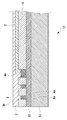
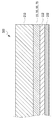
- An example of the typical fragmentary longitudinal cross-section of the electrode peeling film by 1st Embodiment is shown.
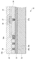
- An example of the typical partial longitudinal cross-sectional view of the color filter substrate with an electrode by 1st Embodiment is shown.
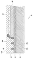
- An example of the typical fragmentary longitudinal cross-section of the electrode peeling film by 2nd Embodiment is shown.
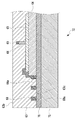
- An example of the typical partial longitudinal cross-sectional view of the color filter substrate with an electrode by 2nd Embodiment is shown.
- An example of the typical fragmentary longitudinal cross-section of the electrode peeling film by 3rd Embodiment is shown.
- An example of the typical fragmentary longitudinal cross-section of the electrode peeling film by 4th Embodiment is shown.
- substrate with an electrode by 4th Embodiment is shown.
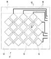
- the example of the typical partial top view which shows the electrode shape of the color filter substrate with an electrode of 2nd Embodiment is shown.
- the example of the typical partial top view which shows the electrode shape of the color filter substrate with an electrode of 4th Embodiment is shown.
- the example of the typical fragmentary longitudinal cross-section of the display apparatus using the color filter substrate with an electrode is shown.
- the example of the typical fragmentary longitudinal cross-section of the display apparatus using the color filter substrate with an electrode is shown.
- the example of the typical fragmentary longitudinal cross-section of the organic electroluminescent display using the color filter substrate with an electrode of this invention is shown.
- First Embodiment 1 and 2 show an example of an electrode peeling film and a color filter substrate with an electrode according to the first embodiment of the present invention.
- the electrode release film 12 of this embodiment includes a film substrate 11, a release layer 10, a resin layer 4, and an adhesive layer 3 in this order.
- the release layer 10 and the resin layer 4 are in direct contact with each other.
- An electrode layer 5 is embedded in the adhesive layer 3.
- the film substrate 11 may be a film having good releasability.
- the material of the film substrate 11 is not particularly limited.
- a plastic film can be used as the film substrate 11.
- polyolefins such as polyethylene and polypropylene, films of 6-nylon, 6,6-nylon, PMMA (polymethyl methacrylate), and the like can be used. If the surface of the film substrate 11 is uneven, there may be problems such as transfer of uneven marks to the resin layer 4 after peeling, or a defect in peeling. Therefore, it is preferable that the surface of the film substrate 11 is smooth.
- a release layer 10 is formed on one surface of the film substrate 11.
- a cured product such as melamine resin, polyolefin resin, urethane resin, or cellulose acetate can be used.
- the thickness of the release layer 10 is not particularly limited. However, the optimum thickness is 0.1 ⁇ m to 3 ⁇ m, for example 1 ⁇ m.
- the release layer can be formed by drying. Examples of the coating method include a die coater, a curtain flow coater, a roll coater, a reverse roll coater, a gravure coater, a knife coater, a bar coater, a spin coater, and a micro gravure coater.
- a resin layer 4 is formed on the surface of the release layer 10 opposite to the film substrate 11.
- the resin layer 4 is a layer obtained by exposing and curing a photosensitive resin, for example.
- the photosensitive resin may be a negative photosensitive resin or a positive photosensitive resin.
- the material of the negative photosensitive resin is not particularly limited.
- the negative photosensitive resin is generally composed of a material containing at least a binder material, a photopolymerizable material, and a photopolymerization initiator.
- materials described in Patent Documents 4 to 6 can be used.
- the material of the positive photosensitive resin is not particularly limited.
- the positive photosensitive resin is generally formed from a material containing an alkali-soluble resin material, a photoacid generating material, an acid-decomposable functional group-containing compound, or the like.
- the positive photosensitive resin for example, materials described in Patent Documents 7 to 9 can be used.
- the photosensitive resin can be formed by applying the above material by various known application methods and then drying.
- the coating method include a die coater, curtain flow coater, roll coater, reverse roll coater, gravure coater, knife coater, bar coater, spin coater, and micro gravure coater.
- the film thickness of the photosensitive resin is preferably 0.1 ⁇ m or more and 25 ⁇ m or less, for example, 5 ⁇ m, but is not limited thereto.
- the photosensitive resin has almost no change in film thickness before and after curing. Therefore, the film thickness is hereinafter described as the film thickness after curing.
- the film thickness is 25 ⁇ m or less, high-definition pattern formation is facilitated.
- the photosensitive resin has a portion soluble in the developer and an insoluble portion by light irradiation through a photomask.
- the portion of the photosensitive resin that is soluble in the developer is dissolved by development to form the groove 4x, and the pattern of the resin layer 4 including the insoluble portion can be formed.
- the developer can be appropriately selected depending on the kind of the photosensitive resin or its material, and can generally be an alkaline aqueous solution or an organic solvent.
- An adhesive layer 3 is formed on the resin layer 4.
- a known heat-sealable adhesive or pressure-sensitive adhesive can be used.
- vinyl acetate resin, ethylene vinyl acetate copolymer resin, vinyl chloride resin, acrylic resin, butyral resin, epoxy resin, polyester resin, polyurethane resin, acrylic adhesive, rubber adhesive, silicon adhesive, urethane Examples include adhesives.
- the thickness of the adhesive layer 3 is optimally in the range of 0.5 ⁇ m to 10 ⁇ m, for example, 2 ⁇ m.
- a separator film (not shown) premised on peeling may be overlaid on the surface 3 b of the adhesive layer 3 opposite to the peeling layer 10.
- the separator film is for preventing the electrode peeling film 12 after the adhesive layer 3 is formed from being bonded when it is wound up in a roll shape or stacked in a flat shape.
- the separator film shall be formed of a thin film of a resin containing a silicone-based material or a fluorine-based material for giving easy peelability to a film made of polyolefin such as polyethylene or polypropylene, PET, PMMA, etc. Can do.
- the electrode layer 5 is embedded in the adhesive layer 3.
- the electrode layer 5 being embedded in the adhesive layer 3 means that at least a part, typically all, of the electrode layer 5 is within the range of the adhesive layer 3 in the height or thickness direction. Including. In the example shown in FIGS. 1 and 2, the electrode layer 5 is sandwiched between the resin layer 4 and the adhesive layer 3.
- the electrode layer 5 as the inorganic compound, any one of indium oxide, zinc oxide, tin oxide, or two or three kinds of mixed oxides thereof, and those added with other additives are used. Can do.
- the electrode layer 5 can use various materials depending on the purpose and application, and is not particularly limited. At present, the most reliable and proven material is indium tin oxide (ITO).
- the most common transparent conductive material for the electrode layer 5 is indium tin oxide (ITO).
- ITO indium tin oxide
- the content ratio of tin oxide doped into indium oxide is selected at an arbitrary ratio according to specifications required for the device.
- a sputtering target material used for crystallizing a thin film for the purpose of increasing mechanical strength preferably has a tin oxide content of less than 10% by weight.
- the content ratio of tin oxide is preferably 10% by weight or more.
- the content rate of a tin oxide has the preferable range of 2 to 20 weight%.
- any film forming method may be used as long as the film thickness can be controlled, and the dry method for forming a thin film is particularly excellent.
- a vacuum vapor deposition method a physical vapor deposition method such as sputtering, or a chemical vapor deposition method such as a CVD method can be used.
- a sputtering method in which the process is stable and the thin film becomes dense is preferable.
- the electrode layer 5 can use materials such as metal nanoparticles, metal nanowires, carbon nanotubes, graphene, and conductive polymers.
- the electrode layer 5 can be formed by coating or drying by dissolving or dispersing in an organic solvent, alcohol, water or the like. In view of sheet resistance and transparency as a transparent conductive film, metal nanowires are more preferably used.
- Metal nanowires can be prepared by mixing with resin and dispersing in water, alcohol, organic solvent, etc. By drying it after coating it, the metal nanowires are entangled with each other to form a network, so that a good electrical conduction path can be formed even with a small amount of conductive material. Thus, the resistance value of the conductive layer can be further reduced. Furthermore, when such a mesh shape is formed, the opening of the gap portion of the mesh is large. Therefore, even if the fibrous conductive substance itself is not transparent, it is possible to achieve good transparency as a coating film.
- the metal of the metal nanowire include iron, cobalt, nickel, copper, zinc, ruthenium, rhodium, palladium, silver, cadmium, osmium, iridium, platinum, and gold. From the viewpoint of conductivity, gold, silver, copper, platinum, and gold are preferable.
- Various known coating methods can be used as a method of forming the electrode layer 5 on the transparent substrate using the metal nanowires or the like.
- Examples of the coating method include spray coating, bar coating, roll coating, die coating, ink jet coating, screen coating, and dip coating.
- the film thickness of the electrode layer 5 is too thin, sufficient conductivity as a conductor tends not to be achieved. If the electrode layer 5 is too thick, the transparency tends to be impaired due to an increase in haze value, a decrease in total light transmittance, and the like. Usually, an appropriate adjustment is made between 10 nm and 10 ⁇ m. However, when the conductive material itself is not transparent like metal nanowires, the transparency can easily be lost by increasing the film thickness, and a conductive layer having a thinner film thickness is often formed. In this case, the conductive layer has an extremely large number of openings. When measured with a contact-type film thickness meter, the average film thickness is preferably in the range of 10 nm to 500 nm, more preferably 30 nm to 300 nm, and most preferably 50 nm to 150 nm.
- a wiring layer 8 is provided adjacent to and in contact with the resin layer 4.
- a groove 4x is provided in the resin layer 4, and a wiring layer 8 is provided in the groove 4x.
- the wiring layer 8 can be formed by conducting a conductive treatment on a wiring material, for example, a precursor of a metal material.
- the precursor of the metal material is mainly composed of metal nanoparticles having a particle diameter of 100 nm or less, for example, metal nanoparticles having a particle diameter of 60 nm, metal oxide nanoparticles, or submicron to several ⁇ m size, or flaky, fibrous or powdery particles.
- Ink, paste or dispersion, or ink containing a metal complex, solution, or the like can be used.
- concentration (solid content concentration) of the metal material precursor, such as ink is 10 wt% or more and 90 wt% or less, for example, 50 wt%, based on the precursor material.
- the metal preferably, at least one element selected from the group consisting of gold, silver, copper, aluminum, iron, titanium, molybdenum, indium, tin, and niobium can be used.
- indium tin oxide is preferably used, and tin oxide, zinc oxide and the like can also be used.
- a conductive carbon material such as graphite, carbon nanotube, graphene, or fullerene may be used. These carbon materials are black and have a characteristic of low reflectance. Therefore, when a display device using a color filter substrate with an electrode is formed, the electrode can be made inconspicuous by disposing it on the side to be visually recognized, which is a more preferable usage example. Even when a carbon material is not used, a compound such as a metal oxide or a metal nitride can be disposed on the side of visual recognition. Thus, an antireflection function can be imparted and the reflectance can be reduced, and the electrode can be made inconspicuous as well.
- the metal material precursor ink and the like can be applied by various known application methods.
- the coating method include a die coater, curtain flow coater, roll coater, reverse roll coater, gravure coater, knife coater, bar coater, spin coater, and micro gravure coater.
- the groove 4x formed in the resin layer 4 can be filled with ink or the like by scraping with a doctor or a squeegee. At this time, it is preferable that the depth of the groove 4x is, for example, 500 nm or more and 10 ⁇ m or less.
- the wiring layer 8 can be formed by firing a metal material precursor or the like conductively.
- the firing method can be appropriately selected according to the material and properties of the precursor.
- a hot air oven, an IR heater, a hot plate, or the like can be used for the thermal baking.
- a xenon flash lamp is used for light baking.
- the film base material 11, the release layer 10, and a resin material layer (not shown; a layer corresponding to the resin layer 4) directly laminated on the release layer 10 are used.
- a laminated body prepared in order is prepared. For example, a film substrate 11 is prepared, and the release layer 10 is applied on the film substrate 11 and dried. What dried and apply
- the resin material layer is developed or molded to form a resin layer having the groove 4x, and a wiring material is applied to the groove 4x to form the wiring layer 8.
- the exposed portion is exposed and developed in a state where the unexposed portion is shielded with a photomask.
- a resin layer having a predetermined pattern is obtained by baking.
- the ink can be scraped off by a doctor. In this way, ink can be embedded in the groove of the resin layer and exposed after drying.
- the electrode layer 5 is laminated on the resin layer 4, and the adhesive layer 3 is laminated on the electrode layer 5 to manufacture the electrode release film 12.
- an electrode material layer is formed by sputtering, patterned after etching by photolithography, and an adhesive layer is applied by printing to produce an electrode release film.
- the electrode peeling film 12 is composed of at least four layers of a film substrate 11, a peeling layer 10, a resin layer 4 that is in direct contact with the peeling layer 10, and an adhesive layer 3 (with the electrode layer 5 embedded). It is composed. Therefore, the electrode peeling film 12 can be configured extremely thin.
- the adhesive layer 3 can be adhered to a transparent substrate or the like later, and the release layer 10 can be peeled (ie, transferred) from the resin layer 4. For this reason, the release layer 10 may be slightly damaged when the resin layer 4 is processed. Thus, the resin layer 4 can be processed without considering the influence on the release layer 10 to be peeled.
- the electrode layer 5 since the electrode layer 5 is embedded in the adhesive layer 3, the electrode layer 5 can be firmly held by the adhesive layer 3. When peeling the release layer 10 from the resin layer 4, the electrode layer 5 can be peeled without peeling. Further, in the example shown in FIG. 1, since the electrode layer 5 is sandwiched between the resin layer 4 and the adhesive layer 3, the electrode layer 5 is firmly held by the resin layer 4 and the adhesive layer 3. can do. When the peeling layer 10 is peeled from the resin layer 4, the peeling layer 10 can be peeled without peeling the electrode layer 5.
- the surface 8 a on the release layer 10 side of the wiring layer 8 and the surface 4 a on the release layer 10 side of the resin layer 4 are located at the same height or are flush with each other. Yes.
- the groove part 4x is provided in the resin layer 4
- the wiring layer 8 is provided in the groove part 4x.
- the adhesive layer 3 is formed on a transparent substrate (a transparent substrate in FIG. 2) on a color filter layer (a layer corresponding to the color filter layer 14 in FIG. 2). 13) is bonded to the glass surface (the surface corresponding to the surface 13a opposite to the color filter layer 14 of the transparent substrate 13 in FIG. 2). Then, the peeling layer 10 is peeled from the resin layer 4, and the color filter substrate 15 with an electrode as shown in FIG. 2 can be produced.
- the electrode-attached color filter substrate 15 of FIG. 2 includes a color filter layer 14, a transparent substrate 13, an adhesive layer 3, and a resin layer 4 in this order.
- the transparent substrate 13 and the adhesive layer 3 are in direct contact with each other.
- An electrode layer 5 is embedded in the adhesive layer 3.
- the transparent substrate 13 glass or a plastic film can be used.
- the transparent substrate 13 is not particularly limited as long as it has sufficient strength in the film forming step and the subsequent step, has excellent transparency, and has good surface smoothness.
- As the glass alkali-free glass for display is preferably used.
- the plastic film include polyethylene terephthalate film, polybutylene terephthalate film, polyethylene naphthalate film, polycarbonate film, polyethersulfone film, polysulfone film, polyarylate film, cyclic polyolefin film, and polyimide film.
- the transparent base material 13 is typically used for the color filter of a display apparatus, it needs to have high transparency, and a thing with a total light transmittance of 85% or more is used suitably.
- the transparent substrate 13 may be subjected to corona treatment, low-temperature plasma treatment, ion bombardment treatment, chemical treatment, or the like as pretreatment for the purpose of improving the adhesion with each layer.
- a color filter layer 14 is formed on the surface of the transparent substrate 13 opposite to the adhesive layer 3.
- the color filter layer 14 typically refers to a layer including at least a black matrix and colored layers of red, green, and blue colors.
- the color filter layer 14 can be formed by applying a colored photosensitive ink, and then exposing and baking.
- the coating method can be, for example, spin coating, spinless coating, inkjet, or the like.
- a transparent electrode may be formed so as to cover the black matrix and the colored layer.
- the colored layer is made of, for example, an acrylic resin having a thickness of 0.5 to 3.0 ⁇ m in which pigments of various colors are dispersed.
- the black matrix is formed of, for example, an acrylic resin having a thickness of 0.5 to 3.0 ⁇ m in which a black pigment is dispersed or a metal film having a thickness of 10 to 200 nm.
- the color filter layer 14 may be a yellow, cyan, magenta, or white (colorless) layer.
- the electrode layer 5 is made of, for example, ITO having a thickness of 10 to 200 nm.
- a transparent resin layer may be formed on the color filter layer 14 for the purpose of flattening and protection.
- An adhesive layer 3, an electrode layer 5, and a resin layer 4 are formed in this order on the surface of the transparent substrate 13 opposite to the color filter layer 14.
- the electrode layer 5, and the resin layer 4 are used as electrodes on the color filter substrate (the transparent base material 13 and the color filter layer 14), the electrode layer 5 acts as an electrode.
- the adhesive layer 3 can bond the adhesive layer 3 to the glass surface of the transparent substrate 13 of the color filter layer 14. Thereafter, the release layer 10 is peeled off together with the film substrate 11. In this way, the color filter substrate 15 with electrodes can be easily formed on the color filter substrate (the transparent base material 13 and the color filter layer 14). This process is called transcription.
- the adhesive layer 3 can be adhered by applying appropriate heat, UV, or pressurization when bonding with materials.
- the wiring layer 8 is preferably disposed so as to overlap the frame portion made of the black material of the color filter layer 14 so that the wiring layer 8 cannot be seen from the viewing side of the display device.
- the color filter substrate 15 with an electrode is directly connected to the color filter substrate 14, the transparent base material 13, the transparent base material 13 (the electrode layer 5 is embedded), and the resin layer 4. It can be composed of at least four layers. Therefore, the electrode-attached color filter substrate 15 can be made extremely thin. That is, the adhesive layer 3 can be bonded to the transparent substrate 13 and the release layer and the like can be already peeled from the resin layer 4. Therefore, the peeling layer and the film base material do not remain even in the color filter substrate 15 with electrodes, and the color filter substrate 15 with electrodes can be configured to be extremely thin.
- the electrode layer 5 since the electrode layer 5 is embedded in the adhesive layer 3, the electrode layer 5 can be firmly held by the adhesive layer 3.
- the electrode layer 5 In the example shown in FIG. 2, the electrode layer 5 is sandwiched between the resin layer 4 and the adhesive layer 3. Therefore, the electrode layer 5 can be firmly held by the resin layer 4 and the adhesive layer 3.
- the surface 8a of the wiring layer 8 opposite to the transparent substrate 13 and the surface 4a of the resin layer 4 opposite to the transparent substrate 13 are located at the same height or flush with each other. Therefore, the wiring layer 8 can be directly connected to an external drive circuit without further processing the resin layer 4.
- [Second Embodiment] 3 to 4 and 9 show examples of the electrode peeling film and the electrode-attached color filter substrate according to the second embodiment of the present invention. In this case, it can be used as a touch sensor on a color filter substrate.
- members that are the same, common, or similar to the materials or members described with respect to the first embodiment are denoted by reference numerals obtained by adding 20 to the reference numerals of the first embodiment in the second embodiment. The description of the embodiment can be cited.
- the resin layer 24 is provided with a further groove 24 y, and the further groove 24 y is provided with a bridge layer 27, and between the bridge layer 27 and the electrode layer 25.
- a transparent insulating layer 26 is provided. Further, the surface 27a of the bridge layer 27 on the release layer 30 side and the surface 24a of the resin layer 24 on the release layer 30 side are located at the same height or are flush with each other.
- the bridge layer (also referred to as a bridge electrode) 27 can be formed by conducting a conductive treatment on a bridge material, for example, a precursor of a metal material.
- the bridge material can be the same as the wiring material of the wiring layer 28.
- the bridge layer 27 and the wiring layer 28 can be simultaneously formed by firing a precursor of a metal material or the like to be conductive, but may be formed separately.
- the reflectance of the wiring layer 8 measured from the opposite side of the color filter layer 14 is preferably 20% or less. This is to make it difficult to visually recognize the bridge layer when it is formed at a position overlapping the display portion of the display device.
- the reflectance was a reflectance in the entire wavelength band from 400 nm to 780 nm measured with a spectrophotometer (Hitachi High-Technologies Corporation, Hitachi spectrophotometer U-4100).
- a transparent insulating layer 26 is formed on the bridge layer 27.
- the transparent insulating layer 26 can be formed of the same material as the resin layer 24 in the same manner. Or it can also form using various printing methods, such as screen printing, an inkjet, gravure offset printing, and flexographic printing.
- the transparent insulating layer 26 is disposed so that the electrode layer 25 and the bridge layer 27 are not electrically short-circuited with each other.
- the transparent insulating layer 26 it is preferable to appropriately select a material capable of obtaining sufficient insulation.
- the film thickness is selected in the range of 0.1 to 10 ⁇ m according to the insulating property, for example, 2 ⁇ m.
- the surface 27 a on the peeling layer 30 side of the bridge layer 27 and the surface 24 a on the peeling layer 30 side of the resin layer 24 are located at the same height or are flush with each other. Yes. Therefore, both side surfaces of the bridge layer 27 are firmly held by the resin layer 24, and the bridge layer 27 can reliably remain in the resin layer 24 when the release layer 30 is peeled from the resin layer 24. Further, the bridge layer 27 does not remain on the release layer 30 and can be peeled well. Since the two surfaces of the resin layer 24 hold the bridge layer 27 firmly, the resin layer 24 can reliably leave the wiring layer 28 when the release layer 30 is peeled from the resin layer 24. Yes. Further, the wiring layer 28 can be satisfactorily peeled without leaving the wiring layer 28 in the peeling layer 30.
- FIG. 5 to 6 show examples of the electrode peeling film and the electrode-attached color filter substrate according to the third embodiment of the present invention.
- 40 and 20 are added to the reference numerals of the first and second embodiments in the third embodiment, respectively.
- the description of 1st, 2nd embodiment can be used, respectively.
- a portion where the resin layer 44 is formed on the release layer 50 and a portion where the resin layer 44 is not formed are formed in a pattern by developing or molding the resin material layer.
- the resin layer 44 is formed, for example, by exposing and developing the exposed portion in a state in which the unexposed portion is shielded with a photomask, washing, drying, and baking to form a resin layer having a predetermined pattern. be able to.
- the electrode layer 45 is formed on the resin layer 44 as an electrode pattern.
- the electrode layer 45 can be formed into a desired pattern by, for example, forming ITO by sputtering and then etching by photolithography.
- the wiring layer 48 can be formed at a location where the resin layer 44 is not formed.
- the wiring layer 48 can be formed by, for example, printing a wiring material, or etching by photolithography after forming a thin film of the wiring material.
- the electrode layer 45 and the wiring layer 48 may be electrically short-circuited and formed as a circuit.
- the adhesive layer 43 is formed between the wiring layers 48, but the resin layer 44 may be formed.
- the surface 48a of the wiring layer 48 on the release layer 50 side and the surface 43a of the adhesive layer 43 on the release layer 50 side are located at the same height or flush with each other.
- a wiring layer 48 is provided between the resin layer 44 and the adhesive layer 43.
- the resin layer 44 and the adhesive layer 43 firmly hold the wiring layer 48, the resin layer 44 and the adhesive layer 43 reliably leave the wiring layer 48 when the release layer 50 is peeled from the resin layer 44. To get. Further, the wiring layer 48 can be satisfactorily peeled without leaving the wiring layer 48 in the peeling layer 50.
- the surface 48a on the release layer 50 side of the wiring layer 48 and the surface 43a on the release layer 50 side of the adhesive layer 43 are located at the same height or are flush with each other. It is sandwiched between layers 43. With the above configuration, since both side surfaces of the wiring layer 48 are firmly held by the adhesive layer 43, the wiring layer 48 reliably remains between the adhesive layers 43 when the release layer 50 is peeled from the resin layer 44. To get. Further, the wiring layer 48 does not remain on the peeling layer 50 and can be peeled well. Since the two surfaces of the adhesive layer 43 hold the wiring layer 48 firmly, the adhesive layer 43 can reliably leave the wiring layer 48 when the release layer 50 is peeled from the resin layer 44. Yes. Further, the wiring layer 48 can be satisfactorily peeled without leaving the wiring layer 48 in the peeling layer 50.
- [Fourth Embodiment] 7 to 8 and 10 show examples of the electrode peeling film and the electrode-attached color filter substrate according to the fourth embodiment of the present invention. Also in this case, it can be used as a touch sensor on the color filter substrate.
- members that are the same, common, or similar to the materials or members described with respect to the first, second, and third embodiments are denoted by the reference numerals of the first, second, and third embodiments in the fourth embodiment. Reference numerals obtained by adding only 60, 40, and 20 can be attached, respectively, and the descriptions of the first, second, and third embodiments can be incorporated respectively.
- a transparent insulating layer 66 is laminated on the electrode layer 65, and a further electrode layer 69 is formed on the transparent insulating layer 66.
- the transparent insulating layer 66 and the further electrode layer 69 are patterned in the same shape as in the electrode peeling film 72 of FIG. 7, the transparent insulating layer 66 and the further electrode layer 69 may be laminated in advance on a uniform plane. it can. Thereafter, a pattern may be formed by developing or etching the transparent insulating layer 66. In this case, it is more preferable to use metal nanowires that can provide good patternability as the electrode layer 65 and the further electrode layer 69.
- each of the electrode layers 65 and 69 can have a pseudo diamond pattern in plan view.
- the inside of the pseudo diamond pattern can be constituted by thin line electrodes.
- a light transmissive electrode pattern can be obtained by setting the fine line width to 5 ⁇ m or less.
- the electrode layer 65 may be partially sandwiched between the resin layer 64 and the adhesive layer 63 by using a part of the surface of the electrode layer 65.
- the electrode layer 65 may be sandwiched indirectly between the resin layer 64 and the adhesive layer 63 via the transparent insulating layer 66 and the further electrode layer 69.
- a plurality of electrode-attached color filter substrates 15, 35, 55, and 75 manufactured as described above may be provided on a single glass substrate.
- a plurality of the color filter substrates with electrodes 15, 35, 55, and 75, or a state in which the color filter substrates are bonded to the TFT substrate are cut into individual pieces, whereby a plurality of them can be efficiently manufactured.
- Examples of the singulation method include diamond cutter scribe processing, dicing processing, water jet processing, etching processing, and laser processing.
- the wiring layers 8, 28, 48, 68 connected to the electrode layers 5, 25, 45, 65 are transferred to a driving IC or the like via an anisotropic conductive adhesive (ACF) and a printed circuit board (FPC).
- ACF anisotropic conductive adhesive
- FPC printed circuit board
- the FPC is thermocompression-bonded to the wiring layers 8, 28, 48, and 68 drawn from the electrode layers 5, 25, 45, and 65 via the ACF, and the FPC is connected to the drive IC of the touch sensor.
- the TFT substrate can be connected to the driving circuit by being connected to the driving IC and the FPC.
- Examples of the display device having the color filter substrate with an electrode of the present invention include a liquid crystal display, an organic EL display, an electronic paper, a MEMS display, a reflective type or a transflective type liquid crystal display.
- Examples of display devices having a liquid crystal layer include those having a structure as shown in FIG.
- a liquid crystal layer 104 is formed between the color filter substrates 15, 35, 55, 75 with electrodes and the TFT substrate 102.
- liquid crystal layers 104 and 204 are formed between the color filter substrates 15, 35, 55 and 75 with electrodes and the TFT substrates 102 and 202.
- Polarizing plates 106 and 206 and cover glasses 110 and 210 are formed in this order on the surface of the color filter substrate with electrodes 15, 35, 55 and 75 opposite to the liquid crystal layers 104 and 204.
- Polarizing plates 106 and 206 and backlights 108 and 208 are sequentially formed on the surface of the TFT substrates 102 and 202 opposite to the liquid crystal layers 104 and 204.
- a plurality of scanning lines are formed on the TFT substrates 102 and 202 at regular intervals.
- a plurality of signal lines are formed at regular intervals on the scanning lines.
- the scanning line and the signal line are arranged so as to intersect with each other via an insulating film.
- a thin film transistor (TFT) that is a switching element is disposed in the vicinity of the intersection of the scanning line and the signal line.
- a display signal is supplied from the signal line to the pixel electrode via the TFT.
- the pixel electrode is formed from a transparent conductive film such as ITO, for example.
- the display area of the liquid crystal display element is composed of a plurality of pixels. The display area is usually formed in a shape close to a rectangle. Further, a frame area provided so as to surround the display area is arranged in the display element.
- the liquid crystal layers 104 and 204 can be formed using a known material and are sealed between the color filter substrates 15, 35, 55, and 75 with electrodes and the TFT substrates 102 and 202.
- an alignment film may be formed on the surface of the color filter layers 14, 34, 54, 74 of the color filter substrates 15, 35, 55, 75 with electrodes and the surfaces of the TFT substrates 102, 202 by a method such as flexographic printing. it can. Thereafter, a rubbing process is performed to enclose the liquid crystal layers 104 and 204, whereby liquid crystal molecules can be aligned in a certain direction.
- the polarizing plates 106 and 206 disposed on both surfaces of the liquid crystal cell have absorption axes in directions almost perpendicular to each other.
- the lighting, gray scale, and extinguishing of each pixel can be determined by the direction of linearly polarized light controlled by the liquid crystal.
- the backlights 108 and 208 are attached to the polarizing plates 106 and 206 on the side opposite to the visual recognition (rear side) with an adhesive or the like.
- the backlights 108 and 208 irradiate the polarizing plates 106 and 206 with planar light.
- the backlights 108 and 208 for example, those having a general configuration including a light source, a light guide plate, a prism sheet, and the like can be used.
- the cover glasses 110 and 210 may be adhered to the four sides of the polarizing plates 106 and 206 on the viewing side or the four sides of the display housing with a double-sided tape or the like, or the entire surface including the display portion of the liquid crystal display using a transparent optical adhesive. May be pasted together.
- the cover glasses 110 and 210 are formed of chemically strengthened glass, transparent resin, or the like. Thereby, the display devices 100 and 200 are completed.
- the liquid crystal cell formed of the color filter substrates 15, 35, 55, and 75 with electrodes, the TFT substrates 102 and 202, and the liquid crystal layers 104 and 204 is used as the polarizing plate 106, Insert at 206. Thereafter, the backlights 108 and 208 are disposed on the back surface, and the cover glasses 110 and 210 are disposed on the display surface. In this manner, a liquid crystal display integrated with display devices 100 and 200, preferably a capacitive touch sensor can be provided.
- the electrodes of the electrode peeling films 12, 32, 52, 72 are transferred in advance to a color filter substrate (a laminate of the color filter layers 14, 34, 54, 74 and the transparent base materials 13, 33, 53, 73), Thereafter, a display may be manufactured.
- the electrodes of the electrode release films 12, 32, 52, and 72 may be transferred and formed on the back surface of the color filter substrate after the display is produced.
- the color filter substrate glass (transparent base materials 13, 33, 53, 73) and the TFT substrate glass in the cellized display are thinned by dissolving them with a chemical solution such as hydrofluoric acid. Is possible.
- the electrodes and the like may be formed in a display device in which the transparent base materials 13, 33, 53, 73 on which the color filter layer 2 is formed are bonded to the TFT substrate to form a cell.
- Examples of the structure of the organic EL display include the example shown in FIG.
- a white organic light emitting layer 112 is formed on TFT substrates 102 and 202 having TFTs formed on glass.
- an organic EL light emitting element structure is formed by forming a transparent upper electrode layer.
- the electrode-attached color filter substrates 15, 35, 55, and 75 are bonded together through a sealant having moisture absorption ability.
- the organic EL display 300 can be obtained by forming a layer that doubles as a capacitive touch sensor, a color filter, and sealing glass.
- the white organic light emitting layer 112 includes a hole transport layer, a hole injection layer, a light emitting layer, an electron injection layer, an electron transport layer, and the like, and can be formed using a known material.
- Example 1 A display device corresponding to the display device 100 of FIG. 11 was manufactured.
- an electrode release film corresponding to the electrode release film of FIG. 3 was prepared.
- a 50 ⁇ m thick PET was prepared as a film substrate, and a urethane resin was applied as a release layer by gravure printing, followed by drying at 40 ° C. for 1 minute.
- a negative photosensitive acrylic resin was applied with a die coater and dried at 90 ° C. for 1 minute. Then, it exposed with the light of 400 mJ / cm ⁇ 2 > in the state which shielded the unexposed part with the photomask.
- a pattern of a photosensitive resin was prepared by baking at 150 ° C. for 3 minutes to obtain a resin layer.
- a portion corresponding to the wiring layer 28 of the color filter substrate 35 with electrodes shown in FIGS. 4 and 9 was formed with a width of 10 ⁇ m, and a portion corresponding to the bridge layer 27 was formed with a width of 3 ⁇ m.
- a copper nanoparticle-carbon particle mixed material was formed as a wiring layer and a bridge layer.
- the ink was scraped off by a doctor.
- the ink was embedded in the pattern made of the photosensitive resin and dried at 120 ° C. for 5 minutes. Then, it was made conductive by irradiating with 5 x J / cm 2 with a xenon flash lamp.
- a transparent insulating layer was formed to a thickness of 2 ⁇ m so as not to cover both ends of the bridge layer.
- a UV curable acrylic resin was used as the transparent insulating layer, and a pattern was applied by screen printing. Then, it hardened
- ITO indium tin oxide
- ITO indium tin oxide
- ITO indium tin oxide
- an electrode layer was formed to a thickness of 30 nm by DC magnetron sputtering, etched by photolithography, and then patterned. In the pattern, a portion corresponding to the electrode layer 25 of the color filter substrate with electrodes 35 of FIGS. At this time, a dry film resist having a thickness of 15 ⁇ m was used as an etching resist.
- a mixture of diluted hydrochloric acid and diluted nitric acid was used as an etchant.
- urethane acrylic resin was applied by gravure printing as an adhesive layer.
- An electrode release film was prepared by overlapping and winding a light release polyethylene film with a silicone release layer.
- a liquid crystal cell was produced as follows. Aluminosilicate glass was used, and the black photosensitive coloring composition was applied on one surface with a spin coater, and dried on a hot plate at 100 ° C. for 5 minutes to dry the coating film. Thereafter, exposure was performed through a photomask having a desired opening at 100 mJ / cm 2 using a high-pressure mercury lamp as a light source. Thereafter, shower development was carried out with a 0.2% by mass aqueous sodium hydrogen carbonate solution for 30 seconds. After washing with water, heat treatment was performed at 230 ° C. for 30 minutes in a hot air circulation oven to form a black matrix pattern. Thereafter, except that the type of the photosensitive coloring composition was changed, red, green and blue patterns were sequentially formed to form a color filter layer. Thus, a color filter substrate including the transparent substrate and the color filter layer was formed.
- an alignment film was formed by printing on the surface of the TFT substrate on which the color filter layer of the color filter substrate and the TFT circuit were formed. Then, it baked at 230 degreeC and performed the rubbing process. Thereafter, the color filter substrate and the TFT substrate were bonded together with a sealing material, and a liquid crystal material was injected into the gap to form a liquid crystal layer, thereby producing a liquid crystal cell.
- the obtained liquid crystal cell was protected by a Teflon (registered trademark) seal and immersed in a hydrofluoric acid aqueous solution at 35 ° C. Thus, the glass portion was chemically polished to a total thickness of 300 ⁇ m.
- the light release film (release layer) of the electrode release film was peeled off from the glass surface on which the color filter layer of the liquid crystal cell subjected to the chemical polishing treatment was formed. Thereafter, the adhesive layer was bonded by a roll press at 120 ° C., and the film substrate was peeled off together with the peeling layer.
- the FPC terminal and the connection terminal of the wiring layer were electrically connected via the ACF, and the touch sensor driving IC was connected.
- the FPC and the liquid crystal driving IC were connected also at the end of the TFT substrate.
- the polarizing plate was affixed on the upper surface of the further electrode layer of a color filter substrate with an electrode, and the lower surface of the TFT substrate, respectively using the adhesive material.
- a backlight was attached to the polarizing plate on the anti-visible (back) side, and chemically strengthened glass was bonded as a cover glass on the visual side (upper) polarizing plate using an optical adhesive.
- a liquid crystal display integrated with a capacitive touch sensor was produced. The display was good and the touch sensor could operate well. Unlike the in-cell structure, the liquid crystal and the touch sensor can be driven separately, making it easier to manufacture than the in-cell structure.
- the liquid crystal display is normally driven by applying an electric field to the liquid crystal by two transparent electrodes formed on the pixel, and controlling the amount of light transmitted through the liquid crystal layer.
- the in-cell structure is usually a structure in which the liquid crystal and the touch sensor are alternately driven by causing one of the transparent electrodes formed in the pixel to have the electrode function of the touch sensor (a common electrode). For this reason, the in-cell structure needs to create an element structure that serves as a wiring or driver for driving the touch sensor on the TFT substrate that drives the liquid crystal.
- the present invention is not limited to the above-described embodiments and examples.
- the shapes of the groove, the wiring layer, the electrode layer, and the like are not limited to those illustrated.
- the design of the present invention can be changed as appropriate based on the knowledge of those skilled in the art.
- a component described in one drawing can be used in place of the component described in another drawing or in addition to the component described in another drawing.
- the resin layer may have a portion where the groove portion is provided and the resin layer is not formed in the surface of the resin layer.
- additional layers may be added inside or outside any two layers.
- the color filter substrate with an electrode of the present invention can be used as a touch panel display in which a liquid crystal display or organic EL display using a color filter and a capacitive touch sensor are integrated, for example, a smartphone, a tablet, a notebook PC, etc. It can be used as a display and user interface.
Landscapes
- Physics & Mathematics (AREA)
- General Physics & Mathematics (AREA)
- Engineering & Computer Science (AREA)
- Theoretical Computer Science (AREA)
- Optics & Photonics (AREA)
- Optical Filters (AREA)
- Devices For Indicating Variable Information By Combining Individual Elements (AREA)
- Laminated Bodies (AREA)
Abstract
本発明は、歩留まり良く、安定に動作し、様々なディスプレイ設計に対応する汎用性を備えた電極剥離フィルム、電極付きカラーフィルタ基板、およびこれらの製造方法を提供することを目的とする。本発明の電極剥離フィルムは、フィルム基材(11、31、51、71)、剥離層(10、30、50、70)、樹脂層(4、24、44、64)、および接着層(3、23、43、63)をこの順に備え、前記剥離層(10、30、50、70)および前記樹脂層(4、24、44、64)が互いに直接接触しており、前記接着層(3、23、43、63)に電極層(5、25、45、65)が埋め込まれていることを特徴とする。
Description
本発明は、電極剥離フィルム、電極付きカラーフィルタ基板、およびこれらの製造方法に関する。好適には、本発明は、静電容量式で動作するタッチセンサのための電極剥離フィルム、電極付きカラーフィルタ基板、およびこれらの製造方法に関する。
近年、様々な電子機器のディスプレイ上に、入力デバイスとして透明なタッチパネルが用いられている。タッチパネルの方式には、抵抗膜式、静電容量式などがある。抵抗膜式は、上下の電極が接触することでタッチ位置を検出する方式である。静電容量式は、指先などが触れた際の表面の静電容量の変化でタッチ位置を検出する方式である。
静電容量式タッチパネルのセンサーは、PETフィルムなどの樹脂基板やガラス基板に電極パターンとして作製され、かつ、一般的には、ディスプレイ構造の外側に配置されるアウトセル構造を有する。(特許文献1)
一方、近年ではタッチセンサをディスプレイ構造に組み込むインセル構造やオンセル構造が採用され始めている。タッチセンサ付きディスプレイをより薄型・軽量化する取り組みがなされている。(特許文献2、特許文献3、特許文献10)
しかしながら、インセル構造はディスプレイ表示の駆動回路であるTFT基板にタッチセンサの回路を組み込む必要があった。この場合、従来から設計やプロセスの煩雑さとそれに伴う良品収率の悪化が伴うことが指摘されていた。またオンセル構造は、特に液晶ディスプレイの場合、液晶を封入したセルの状態でタッチセンサを形成する。そのため、熱などのプロセス条件による液晶へのダメージを考慮したプロセス設計に課題があった。また薄型化した液晶セルに対し、複雑なタッチセンサ形成工程を経ることで良品収率の悪化が生じていた。
本発明の課題の1つは、歩留まり良く、安定に動作し、様々なディスプレイ設計に対応する汎用性を備えた電極剥離フィルム、電極付きカラーフィルタ基板、およびこれらの製造方法を提供することである。好適には、本発明の課題は、タッチセンサが一体化したディスプレイの作製にあたり、上記のような従来技術の課題を解決することである。
本発明の課題を解決するための手段の一例は、フィルム基材(11、31、51、71)、剥離層(10、30、50、70)、樹脂層(4、24、44、64)、および接着層(3、23、43、63)をこの順に備え、前記剥離層(10、30、50、70)および前記樹脂層(4、24、44、64)が互いに直接接触しており、前記接着層(3、23、43、63)に電極層(5、25、45、65)が埋め込まれていることを特徴とする電極剥離フィルムである。
ここで、前記電極層(5、25、45、65)が、前記樹脂層(4、24、44、64)と前記接着層(3、23、43、63)との間で挟持されていることが好ましい。
また、配線層(8、28、48、68)が、前記樹脂層(4、24、44、64)と隣り合って接して設けられていることが好ましい。さらに、配線層(8、28、48、68)が設けられていて、前記配線層(8、28、48、68)の前記剥離層(10、30、50、70)側の表面(8a、28a、48a、68a)と、前記樹脂層(4、24、44、64)の前記剥離層(10、30、50、70)側の表面(4a、24a、44a、64a)とが、同じ高さに位置するかまたは面一となっていることが好ましい。あるいは、配線層(8、28)が設けられていて、前記樹脂層(4、24)に溝部(4x、24x)が設けられていて、前記溝部(4x、24x)に前記配線層(8、28)が設けられていることが好ましい。
また、前記樹脂層(24)に更なる溝部(24y)が設けられていて、前記更なる溝部(24y)にブリッジ層(27)が設けられていて、前記ブリッジ層(27)と前記電極層(25)との間に透明絶縁層(26)が設けられていることが好ましい。さらに、前記ブリッジ層(27)の前記剥離層(30)側の表面(27a)と、前記樹脂層(24)の前記剥離層(30)側の表面(24a)とが、同じ高さに位置するかまたは面一となっていることが好ましい。
あるいは、配線層(48、68)が設けられていて、前記配線層(48、68)の前記剥離層(50、70)側の表面(48a、68a)と、前記接着層(43、63)の前記剥離層(50、70)側の表面(43a、63a)とが、同じ高さに位置するかまたは面一となっていることが好ましい。また、配線層(48、68)が、前記接着層(43、63)に挟持されて設けられていることが好ましい。
ここで、前記樹脂層(4、24、44、64)が、感光性樹脂を光硬化した材料を含んでもよく、あるいは前記樹脂層(4、24、44、64)が、熱可塑性樹脂を成型加工した樹脂であってもよい。
また、前記接着層(3、23、43、63)の前記剥離層(10、30、50、70)と反対側の表面(3b、23b)に、セパレータフィルムが設けられていてもよい。
本発明の課題を解決するための手段の別の例は、カラーフィルタ層(14、34、54、74)、透明基材(13、33、53、73)、接着層(3、23、43、63)、および樹脂層(4、24、44、64)をこの順に備え、前記透明基材(13、33、53、73)および前記接着層(3、23、43、63)が互いに直接接触しており、前記接着層(3、23、43、63)に電極層(5、25、45、65)が埋め込まれていることを特徴とする電極付きカラーフィルタ基板である。
ここで、前記電極層(5、25、45、65)が、前記接着層(3、23、43、63)と前記樹脂層(4、24、44、64)との間で挟持されていることが好ましい。
また、配線層(8、28、48、68)が、前記樹脂層(4、24、44、64)と隣り合って接して設けられていることが好ましい。さらに、配線層(8、28、48、68)が設けられていて、前記配線層(8、28、48、68)の前記透明基材(13、33、53、73)と反対側の表面(8a、28a、48a、68a)と、前記樹脂層(4、24、44、64)の前記透明基材(13、33、53、73)と反対側の表面(4a、24a、44a、64a)とが、同じ高さに位置するかまたは面一となっていることが好ましい。あるいは、配線層(8、28)が設けられていて、前記樹脂層(4、24)に溝部(4x、24x)が設けられていて、前記溝部(4x、24x)に前記配線層(8、28)が設けられていることが好ましい。
また、前記樹脂層(24)に更なる溝部(24y)が設けられていて、前記更なる溝部(24y)にブリッジ層(27)が設けられていて、前記ブリッジ層(27)と前記電極層(25)との間に透明絶縁層(26)が設けられていることが好ましい。さらに、前記ブリッジ層(27)の前記透明基材(33)と反対側の表面(27a)と、前記樹脂層(24)の前記透明基材(33)と反対側の表面(24a)とが、同じ高さに位置するかまたは面一となっていることが好ましい。
あるいは、配線層(48、68)が設けられていて、前記配線層(48、68)の前記透明基材(53、73)と反対側の表面(48a、68a)と、前記接着層(43、63)の前記透明基材(53、73)と反対側の表面(43a、63a)とが、同じ高さに位置するかまたは面一となっていることが好ましい。また、配線層(48、68)が、前記接着層(43、63)に挟持されて設けられていることが好ましい。
ここで、前記樹脂層(4、24、44、64)が、感光性樹脂を光硬化した材料を含んでもよく、あるいは前記樹脂層(4、24、44、64)が、熱可塑性樹脂を成型加工した樹脂であってもよい。
また、配線層(8、28、48、68)が設けられていて、前記カラーフィルタ層(14、34、54、74)の反対側から測定した前記配線層(8、28、48、68)の反射率が20%以下であることが好ましい。
本発明の課題を解決するための手段の更に別の例は、前述の電極付きカラーフィルタ基板を設けた表示装置である。
本発明の課題を解決するための手段の更に別の例は、フィルム基材(11、31)、剥離層(10、30)、および前記剥離層(10、30)の上に直接積層された樹脂材料層をこの順に備えた積層体を準備する工程と、前記樹脂材料層を現像または成型して溝部(4x、24x)を備えた樹脂層(4、24)を形成する工程と、前記溝部(4x、24x)に配線材料を塗布して配線層(8、28)を形成する工程と、前記樹脂層(4、24)の上に電極層(5、25)を積層する工程と、前記電極層(5、25)の上に接着層(3、23)を積層する工程と、を含む、電極剥離フィルムの製造方法である。
ここで、前記溝部(4x、24x)に前記配線材料を塗布する工程は、前記配線材料をインク状にしたものをスキージ状またはドクター状の部材で掻くことで、前記溝部(4x、24x)に前記配線材料を埋め込む工程であることが好ましい。
また、前記樹脂材料層を現像または成型して更なる溝部(24y)を備えた樹脂層(24)を形成する工程と、前記更なる溝部(24y)にブリッジ材料を塗布してブリッジ層(27)を形成する工程と、前記ブリッジ層(27)の上に透明絶縁層(26)を積層する工程と、前記透明絶縁層(26)の上に電極層(25)を積層する工程と、を含むことが好ましい。
さらに、前記樹脂材料層を現像または成型して溝部(24x)を備えた樹脂層(24)を形成する工程と、前記樹脂材料層を現像または成型して更なる溝部(24y)を備えた樹脂層(24)を形成する工程とが同時に行われることが好ましい。また、前記溝部(4x)に前記配線材料を塗布する工程と、前記更なる溝部(24y)に前記ブリッジ材料を塗布する工程とが、同時に行われることが好ましい。
本発明の課題を解決するための手段の更に別の例は、フィルム基材(51、71)、剥離層(50、70)、および前記剥離層(50、70)の上に直接積層された樹脂材料層をこの順に備えた積層体を準備する工程と、前記樹脂材料層を現像または成型して前記剥離層(50、70)上に樹脂層(44、64)が形成された箇所と形成されて無い箇所をパターン状に形成する工程と、前記樹脂層(44、64)が形成されて無い箇所に配線層(48、68)を形成する工程と、前記樹脂層(44、64)の上に電極層(45、65)を形成する工程と、前記電極層(45、65)の上に接着層(43、63)を積層する工程と、を含む、電極剥離フィルムの製造方法である。
ここで、前記樹脂層(44、64)が形成されて無い箇所に配線層(48、68)を形成する工程は、配線材料を印刷する工程、あるいは配線材料の薄膜形成後フォトリソグラフィーでパターン形成する工程であることが好ましい。
また、前記電極層(65)の上に透明絶縁層(66)を積層する工程と、前記透明絶縁層(66)の上に更なる電極層(69)を形成する工程と、を更に含むことが好ましい。
本発明の課題を解決するための手段の更に別の例は、カラーフィルタ層(14、34、54、74)および透明基材(13、33、53、73)を積層した積層体を準備する工程と、前記製造方法により製造された電極剥離フィルム(12、32、52、72)の前記接着層(3、23、43、63)の、前記剥離層(10、30、50、70)と反対側の表面(3b、23b、43b、63b)を、前記透明基材(13、33、53、73)の前記カラーフィルタ層(14、34、54、74)と反対側の表面(13a、33a、53a、73a)に張り合わせる工程と、前記剥離層(10、30、50、70)を、前記樹脂層(4、24、44、64)から剥離する工程と、を含む電極付きカラーフィルタ基板の製造方法である。
本発明の課題を解決するための手段の更に別の例は、前述の電極付きカラーフィルタ基板の製造方法を含む、表示装置の製造方法であって、前記カラーフィルタ層(14、34、54、74)の、前記透明基材(13、33、53、73)と反対側の表面に、TFT基板が予め貼り合わされており、前記電極層(5、25、45、65)タッチセンサの駆動回路に電気的に接続する工程を更に含む、表示装置の製造方法である。
本発明によれば、歩留まり良く、または安定に動作し、または様々なディスプレイ設計に対応する汎用性を備えた電極剥離フィルム、電極付きカラーフィルタ基板、およびこれらの製造方法が提供され得る。
以下、本発明を実施するための形態を、図面を用いて説明する。
[第1実施形態]
図1~2において、本発明の第1実施形態の電極剥離フィルムおよび電極付きカラーフィルタ基板の例を示す。
図1~2において、本発明の第1実施形態の電極剥離フィルムおよび電極付きカラーフィルタ基板の例を示す。
≪電極剥離フィルム≫
本実施形態の電極剥離フィルム12は、フィルム基材11、剥離層10、樹脂層4、および接着層3をこの順に備える。剥離層10および樹脂層4が互いに直接接触している。接着層3に電極層5が埋め込まれている。
本実施形態の電極剥離フィルム12は、フィルム基材11、剥離層10、樹脂層4、および接着層3をこの順に備える。剥離層10および樹脂層4が互いに直接接触している。接着層3に電極層5が埋め込まれている。
<フィルム基材>
フィルム基材11は、離型性の良いフィルムであればよい。フィルム基材11の材料は特に限定されない。フィルム基材11として、離型性を付与するためのシリコーン系材料やフッ素系材料を含有する樹脂を薄膜で形成したものが好適に用いられる。フィルム基材11としてプラスチックフィルムを使用できる。それに加え、ポリエチレン、ポロプロピレンなどのポリオレフィン、6-ナイロン、6,6-ナイロン、PMMA(ポリメタクリル酸メチル)などのフィルムを用いることができる。フィルム基材11の表面に凹凸があると剥離後の樹脂層4に凹凸跡が転写されたり、剥離に不良が生じるなどの問題が発生したりする場合がある。そのため、フィルム基材11の表面は平滑であることが好ましい。
フィルム基材11は、離型性の良いフィルムであればよい。フィルム基材11の材料は特に限定されない。フィルム基材11として、離型性を付与するためのシリコーン系材料やフッ素系材料を含有する樹脂を薄膜で形成したものが好適に用いられる。フィルム基材11としてプラスチックフィルムを使用できる。それに加え、ポリエチレン、ポロプロピレンなどのポリオレフィン、6-ナイロン、6,6-ナイロン、PMMA(ポリメタクリル酸メチル)などのフィルムを用いることができる。フィルム基材11の表面に凹凸があると剥離後の樹脂層4に凹凸跡が転写されたり、剥離に不良が生じるなどの問題が発生したりする場合がある。そのため、フィルム基材11の表面は平滑であることが好ましい。
<剥離層>
フィルム基材11の片面には剥離層10が形成されている。剥離層10としては、メラミン樹脂、ポリオレフィン樹脂、ウレタン樹脂、酢酸セルロースなどの硬化物が使用可能である。剥離層10の厚みは、特に制限が無い。しかしながら、その厚みは0.1μm~3μmが最適であり、例えば1μmである。剥離層を形成するための材料を種々の公知の塗布方法で塗布した後、乾燥することで剥離層を形成できる。前記塗布方法は、例えばダイコーター、カーテンフローコーター、ロールコーター、リバースロールコーター、グラビアコーター、ナイフコーター、バーコーター、スピンコーター、マイクログラビアコーターなどのを挙げることができる。
フィルム基材11の片面には剥離層10が形成されている。剥離層10としては、メラミン樹脂、ポリオレフィン樹脂、ウレタン樹脂、酢酸セルロースなどの硬化物が使用可能である。剥離層10の厚みは、特に制限が無い。しかしながら、その厚みは0.1μm~3μmが最適であり、例えば1μmである。剥離層を形成するための材料を種々の公知の塗布方法で塗布した後、乾燥することで剥離層を形成できる。前記塗布方法は、例えばダイコーター、カーテンフローコーター、ロールコーター、リバースロールコーター、グラビアコーター、ナイフコーター、バーコーター、スピンコーター、マイクログラビアコーターなどのを挙げることができる。
<樹脂層>
剥離層10のフィルム基材11と反対側の表面には樹脂層4が形成されている。樹脂層4は、例えば感光性樹脂を露光して硬化させた層である。感光性樹脂は、ネガ型感光性樹脂としても良いし、ポジ型感光性樹脂としても良い。ネガ型感光性樹脂の材料は特に限定されない。しかしながら、ネガ型感光性樹脂は、一般的に、バインダー材料、光重合性材料、光重合開始剤を少なくとも含有する材料から構成される。ネガ型感光性樹脂として、例えば特許文献4~6に記載の材料を用いることができる。また、ポジ型感光性樹脂の材料は特に限定されない。しかしながら、ポジ型感光性樹脂は、一般的に、アルカリ可溶性樹脂材料、光酸発生材料、酸分解性官能基含有化合物等を含有する材料から形成される。ポジ型感光性樹脂として、例えば特許文献7~9に記載の材料を用いることができる。
剥離層10のフィルム基材11と反対側の表面には樹脂層4が形成されている。樹脂層4は、例えば感光性樹脂を露光して硬化させた層である。感光性樹脂は、ネガ型感光性樹脂としても良いし、ポジ型感光性樹脂としても良い。ネガ型感光性樹脂の材料は特に限定されない。しかしながら、ネガ型感光性樹脂は、一般的に、バインダー材料、光重合性材料、光重合開始剤を少なくとも含有する材料から構成される。ネガ型感光性樹脂として、例えば特許文献4~6に記載の材料を用いることができる。また、ポジ型感光性樹脂の材料は特に限定されない。しかしながら、ポジ型感光性樹脂は、一般的に、アルカリ可溶性樹脂材料、光酸発生材料、酸分解性官能基含有化合物等を含有する材料から形成される。ポジ型感光性樹脂として、例えば特許文献7~9に記載の材料を用いることができる。
感光性樹脂は、種々の公知の塗布方法で上記材料を塗布した後、乾燥することで形成できる。前記塗布方法は、ダイコーター、カーテンフローコーター、ロールコーター、リバースロールコーター、グラビアコーター、ナイフコーター、バーコーター、スピンコーター、マイクログラビアコーターなどを挙げることができる。感光性樹脂の膜厚は、0.1μm以上25μm以下であることが好ましく、例えば5μmであるがこの限りではない。典型的には、感光性樹脂は、硬化前後でほとんど膜厚の変化はない。そのため、膜厚は、以後、硬化後の膜厚で記載される。好ましくは、膜厚が25μm以下であると高精細パターン形成が容易となる。膜厚が0.1μm以上であると形成ムラ等の外観上の歪みが発生せず、また隣接する層との十分な密着性を示す。感光性樹脂は、フォトマスクを介した光照射により、現像液に可溶な部分と不溶な部分ができる。感光性樹脂の現像液に可溶な部分は現像により溶解して溝部4xとなり、不溶な部分からなる樹脂層4のパターンを形成できる。現像液は感光性樹脂またはその材料の種類により適宜選択でき、一般的にアルカリ水溶液または有機溶剤とすることができる。
<接着層>
樹脂層4の上には、接着層3が形成されている。接着層3としては、公知のヒートシール性接着剤または粘着剤を使用できる。例えば、酢酸ビニル樹脂、エチレン酢酸ビニル共重合樹脂、塩酢ビ樹脂、アクリル樹脂、ブチラール樹脂、エポキシ樹脂、ポリエステル樹脂、ポリウレタン樹脂、アクリル系粘着剤、ゴム系粘着剤、シリコン系粘着剤、ウレタン系粘着剤などがあげられる。接着層3の厚みとしては、0.5μm~10μmの範囲が最適であり、例えば2μmとする。
樹脂層4の上には、接着層3が形成されている。接着層3としては、公知のヒートシール性接着剤または粘着剤を使用できる。例えば、酢酸ビニル樹脂、エチレン酢酸ビニル共重合樹脂、塩酢ビ樹脂、アクリル樹脂、ブチラール樹脂、エポキシ樹脂、ポリエステル樹脂、ポリウレタン樹脂、アクリル系粘着剤、ゴム系粘着剤、シリコン系粘着剤、ウレタン系粘着剤などがあげられる。接着層3の厚みとしては、0.5μm~10μmの範囲が最適であり、例えば2μmとする。
剥離することを前提としたセパレータフィルム(図示省略)を、接着層3の剥離層10と反対側の表面3b上に重ねても良い。セパレータフィルムは、接着層3を形成した後の電極剥離フィルム12をロール状に巻き取ったり、平面状に重ねたりする際に接着してしまわないようにするためのものである。セパレータフィルムは、例えばポリエチレンやポリプロピレンなどのポリオレフィン、PET、PMMAなどから成るフィルムに対し、易剥離性を持たせるためのシリコーン系材料やフッ素系材料を含有する樹脂を薄膜で形成したものとすることができる。
<電極層>
電極層5は、接着層3に埋め込まれている。なお、電極層5が接着層3に埋め込まれているとは、電極層5の少なくとも一部、典型的には全部が接着層3の高さまたは厚さ方向の範囲内にあることの意味を含む。図1~2に示された例においては、電極層5は、樹脂層4と接着層3との間で挟持されている。電極層5として、無機化合物としては酸化インジウム、酸化亜鉛、酸化スズのいずれか、または、それらの2種類もしくは3種類の混合酸化物、さらには、その他添加物が加えられた物などを用いることができる。しかしながら、電極層5は、目的・用途により種々の材料を使用でき、特に限定されるものではない。現在のところ、最も信頼性が高く、多くの実績のある材料は酸化インジウムスズ(ITO)である。
電極層5は、接着層3に埋め込まれている。なお、電極層5が接着層3に埋め込まれているとは、電極層5の少なくとも一部、典型的には全部が接着層3の高さまたは厚さ方向の範囲内にあることの意味を含む。図1~2に示された例においては、電極層5は、樹脂層4と接着層3との間で挟持されている。電極層5として、無機化合物としては酸化インジウム、酸化亜鉛、酸化スズのいずれか、または、それらの2種類もしくは3種類の混合酸化物、さらには、その他添加物が加えられた物などを用いることができる。しかしながら、電極層5は、目的・用途により種々の材料を使用でき、特に限定されるものではない。現在のところ、最も信頼性が高く、多くの実績のある材料は酸化インジウムスズ(ITO)である。
電極層5として最も一般的な透明導電材は、酸化インジウムスズ(ITO)である。酸化インジウムスズ(ITO)を電極層5として用いる場合、酸化インジウムにドープされる酸化スズの含有比はデバイスに求められる仕様に応じて、任意の割合を選択する。例えば、機械強度を高める目的で薄膜を結晶化させるために用いるスパッタリングターゲット材料は、酸化スズの含有比が10重量%未満であることが好ましい。薄膜をアモルファス化しフレキシブル性を持たせるためには、酸化スズの含有比は10重量%以上が好ましい。また、薄膜に低抵抗が求められる場合は、酸化スズの含有比は2重量%から20重量%の範囲が好ましい。
電極層5の製造方法としては、膜厚の制御が可能であればいかなる成膜方法でも良く、なかでも薄膜形成の乾式法が優れている。前記成膜方法として、真空蒸着法、スパッタリングなどの物理的気相析出法やCVD法のような化学的気相析出法を用いることができる。特に大面積に均一な膜質の薄膜を形成するために、プロセスが安定し、薄膜が緻密化するスパッタリング法が好ましい。
電極層5は金属ナノ粒子や金属ナノワイヤー、カーボンナノチューブ、グラフェン、導電性高分子などの材料を用いることができる。電極層5は、有機溶剤やアルコール、水などに溶解あるいは分散させることで、塗工、乾燥により形成することができる。さらに透明導電膜としてのシート抵抗や透明性を鑑みて、より好適には金属ナノワイヤーが用いられる。
金属ナノワイヤーは樹脂等と混合し、水やアルコール、有機溶剤などに分散することで調液することができる。それを塗工後、乾燥することで、金属ナノワイヤーが互いに絡み合って網の目状となることで、少ない量の導電性物質であっても良好な電気伝導経路を形成することができる。こうして、導電層の抵抗値をより低下させることができる。さらにこのような網の目状を形成した場合、網の目の隙間部分の開口が大きい。そのため、たとえ繊維状の導電性物質そのものが透明でなかったとしても、塗膜として良好な透明性を達成することが可能である。
金属ナノワイヤーの金属として、具体的には鉄、コバルト、ニッケル、銅、亜鉛、ルテニウム、ロジウム、パラジウム、銀、カドミウム、オスミウム、イリジウム、白金、金を挙げることができる。導電性の観点から、金、銀、銅、白金、金が好ましい。
前記金属ナノワイヤー等を用いて透明基板上に電極層5を形成する方法として種々の公知の塗布方法を用いることができる。前記塗布方法は、例えばスプレーコート、バーコート、ロールコート、ダイコート、インクジェットコート、スクリーンコート、ディップコートなどを挙げることができる。
電極層5の膜厚は薄すぎると導体としての十分な導電性が達成出来なくなる傾向にある。電極層5の膜厚が厚すぎるとヘイズ値の上昇、全光線透過率の低下等で透明性が損なわれる傾向にある。通常は10nm~10μmの間で適宜調整を行う。しかしながら、金属ナノワイヤーのように導電性物質そのものが透明でない場合には、膜厚の増加によって透明性が失われ得やすく、より薄い膜厚の導電層が形成されることが多い。この場合きわめて開口部の多い導電層である。接触式の膜厚計で測定したときに平均膜厚として10nm~500nmの膜厚範囲がこのましく、30nm~300nmがより好ましく、50nm~150nmが最も好ましい。
<配線層>
配線層8が、樹脂層4と隣り合って接して設けられている。図1~2に示された例においては、樹脂層4に溝部4xが設けられていて、溝部4xに配線層8が設けられている。配線層8は、配線材料、例えば金属材料の前駆体を導電性処理することにより形成することができる。金属材料の前駆体は、粒子径100nm以下、例えば粒子径60nmの金属ナノ粒子、あるいは金属酸化物ナノ粒子、あるいはサブミクロンから数μmサイズ、あるいはフレーク状、繊維状、粉状の粒子を主原料としたインク、ペーストあるいは分散液、または金属錯体を含むインク、溶液等を用いることができる。金属材料の前駆体のインク等の濃度(固形分濃度)は、前駆体材料を基準として10wt%以上90wt%以下、例えば50wt%である。金属としては、好ましくは金、銀、銅、アルミニウム、鉄、チタン、モリブデン、インジウム、錫、およびニオブからなる群から選ばれる少なくとも1種の元素を用いることができる。金属酸化物を用いる場合、酸化インジウムスズが好適に使用され、他に酸化スズ、酸化亜鉛等を用いることができる。また、金属材料の代わりに、グラファイト、カーボンナノチューブ、グラフェン、フラーレン等の導電性を有する炭素材料を用いてもよい。これら炭素材料は黒色であり、低い反射率という特徴を持つ。そのため、電極付きカラーフィルタ基板を用いた表示装置を形成した時に、視認する側に配置することで電極を目立たなくすることが可能であり、これがより好ましい使用例である。炭素材料を用いない場合も、金属酸化物、あるいは金属窒化物などの化合物を視認する側に配置することができる。こうして反射防止機能を付与し、反射率低減することができ、同様に電極を目立たなくすることができる。
配線層8が、樹脂層4と隣り合って接して設けられている。図1~2に示された例においては、樹脂層4に溝部4xが設けられていて、溝部4xに配線層8が設けられている。配線層8は、配線材料、例えば金属材料の前駆体を導電性処理することにより形成することができる。金属材料の前駆体は、粒子径100nm以下、例えば粒子径60nmの金属ナノ粒子、あるいは金属酸化物ナノ粒子、あるいはサブミクロンから数μmサイズ、あるいはフレーク状、繊維状、粉状の粒子を主原料としたインク、ペーストあるいは分散液、または金属錯体を含むインク、溶液等を用いることができる。金属材料の前駆体のインク等の濃度(固形分濃度)は、前駆体材料を基準として10wt%以上90wt%以下、例えば50wt%である。金属としては、好ましくは金、銀、銅、アルミニウム、鉄、チタン、モリブデン、インジウム、錫、およびニオブからなる群から選ばれる少なくとも1種の元素を用いることができる。金属酸化物を用いる場合、酸化インジウムスズが好適に使用され、他に酸化スズ、酸化亜鉛等を用いることができる。また、金属材料の代わりに、グラファイト、カーボンナノチューブ、グラフェン、フラーレン等の導電性を有する炭素材料を用いてもよい。これら炭素材料は黒色であり、低い反射率という特徴を持つ。そのため、電極付きカラーフィルタ基板を用いた表示装置を形成した時に、視認する側に配置することで電極を目立たなくすることが可能であり、これがより好ましい使用例である。炭素材料を用いない場合も、金属酸化物、あるいは金属窒化物などの化合物を視認する側に配置することができる。こうして反射防止機能を付与し、反射率低減することができ、同様に電極を目立たなくすることができる。
金属材料の前駆体のインク等は、種々の公知の塗布方法で塗布することができる。前記塗布方法は、例えばダイコーター、カーテンフローコーター、ロールコーター、リバースロールコーター、グラビアコーター、ナイフコーター、バーコーター、スピンコーター、マイクログラビアコーターなどを挙げることができる。前記塗布方法で塗布した後、ドクターあるいはスキージで掻き取ることで、樹脂層4に形成された溝部4xにインク等を充填することができる。この時、溝部4xの深さは例えば500nm以上10μm以下で形成するのが好ましい。
配線層8は、金属材料の前駆体等を導電性に焼成することにより形成することができる。焼成方法は、前駆体の材料や性質に応じて適宜選択できる。熱焼成には熱風オーブン、IRヒータ、ホットプレートなどを用いることができる。光焼成としてはキセノンフラッシュランプを用いることが一般的である。また、薬液処理により導電性を付与しても良い。
電極剥離フィルム12を製造する際には、フィルム基材11、剥離層10、および剥離層10の上に直接積層された樹脂材料層(図示せず。樹脂層4に相当する層。)をこの順に備えた積層体を準備する。例えば、フィルム基材11を用意し、フィルム基材11上に剥離層10を塗布して乾燥する。これに樹脂材料を塗布して乾燥したものを上記積層体として準備することができる。
続いて、樹脂材料層を現像または成型して溝部4xを備えた樹脂層を形成し、溝部4xに配線材料を塗布して配線層8を形成する。例えば、フォトマスクで未露光部を遮光した状態で露光部を感光させて現像する。洗浄乾燥後、ベークすることで所定のパターンを有する樹脂層とする。続いて、配線材料として導電性のインクを印刷により樹脂層上にコートした後、ドクターでインクを掻き取ることができる。こうして、樹脂層の溝にインクを埋め込み、乾燥後露光することができる。
続いて、樹脂層4の上に電極層5を積層し、電極層5の上に接着層3を積層して、電極剥離フィルム12を製造する。例えば、電極材料層をスパッタにより成膜し、フォトリソグラフィーによりエッチング後パターニングし、更に接着層を印刷で塗布することで電極剥離フィルムを作製する。
本実施形態においては、電極剥離フィルム12を、フィルム基材11、剥離層10、剥離層10に直接接触する樹脂層4、および(電極層5が埋め込まれた)接着層3の少なくとも4層で構成している。そのため、電極剥離フィルム12を極めて薄く構成できる。また、後に接着層3を透明基材等に接着するとともに剥離層10を樹脂層4から剥離(すなわち転写)できるようになっている。そのため、樹脂層4を加工する際に剥離層10が多少痛んでも良いようになっている。こうして、剥離される剥離層10への影響を考慮することなく樹脂層4を加工することができるようになっている。
特に、接着層3に電極層5が埋め込まれているので、接着層3によって電極層5を強固に保持することができる。樹脂層4から剥離層10を剥離する際に、電極層5を剥離することなく剥離できる。また、図1に示された例においては、電極層5が、樹脂層4と接着層3との間で挟持されているいため、樹脂層4と接着層3とによって電極層5を強固に保持することができる。樹脂層4から剥離層10を剥離する際に、電極層5を剥離することなく剥離層10を剥離できるようになっている。
図1に示された例においては、配線層8の剥離層10側の表面8aと、樹脂層4の剥離層10側の表面4aとは、同じ高さに位置するかまたは面一となっている。また、樹脂層4に溝部4xが設けられていて、溝部4xに配線層8が設けられている。上記構成により、配線層8の両側面が樹脂層4に強固に保持されるようになっている。剥離層10を樹脂層4から剥離する際に、配線層8が樹脂層4に確実に残存し、剥離層10に配線層8が残存することなく、良好に剥離できるようになっている。樹脂層4の2面が配線層8を強固に保持している。そのため、剥離層10が樹脂層4から剥離される際に、樹脂層4が配線層8を確実に残存させ、剥離層10に配線層8を残存させることなく、良好に剥離できるようになっている。
図1に示したような電極剥離フィルム12を作製した後、例えば、接着層3をカラーフィルタ層(図2のカラーフィルタ層14に相当する層)上の透明基材(図2の透明基材13に相当する層)のガラス面(図2の透明基材13のカラーフィルタ層14と反対側の表面13aに相当する面)に貼り合わせる。その後、剥離層10を樹脂層4から剥離することで、図2に示したような電極付きカラーフィルタ基板15を作製することができる。
≪電極付きカラーフィルタ基板≫
図2の電極付きカラーフィルタ基板15は、カラーフィルタ層14、透明基材13、接着層3、および樹脂層4をこの順に備える。透明基材13および接着層3が互いに直接接触している。接着層3に電極層5が埋め込まれている。
図2の電極付きカラーフィルタ基板15は、カラーフィルタ層14、透明基材13、接着層3、および樹脂層4をこの順に備える。透明基材13および接着層3が互いに直接接触している。接着層3に電極層5が埋め込まれている。
<透明基材>
透明基材13として、ガラスまたはプラスチックフィルムを用いることができる。透明基材13は、成膜工程および後工程において十分な強度があり、優れた透明性を有し、表面の平滑性が良好であれば特に限定されない。ガラスとしてはディスプレイ用途の無アルカリガラスが好適に使用される。プラスチックフィルムとしては、例えば、ポリエチレンテレフタレートフィルム、ポリブチレンテレフタレートフィルム、ポリエチレンナフタレートフィルム、ポリカーボネートフィルム、ポリエーテルスルホンフィルム、ポリスルホンフィルム、ポリアリレートフィルム、環状ポリオレフィンフィルム、ポリイミドフィルムなどが挙げられる。また、透明基材13は、典型的には表示装置のカラーフィルタに用いられるため、高い透明性を有することが必要で、全光線透過率が85%以上のものが好適に使用される。透明基材13は、各層との密着性を改善する目的で、前処理としてコロナ処理、低温プラズマ処理、イオンボンバード処理、薬品処理などを施してもよい。
透明基材13として、ガラスまたはプラスチックフィルムを用いることができる。透明基材13は、成膜工程および後工程において十分な強度があり、優れた透明性を有し、表面の平滑性が良好であれば特に限定されない。ガラスとしてはディスプレイ用途の無アルカリガラスが好適に使用される。プラスチックフィルムとしては、例えば、ポリエチレンテレフタレートフィルム、ポリブチレンテレフタレートフィルム、ポリエチレンナフタレートフィルム、ポリカーボネートフィルム、ポリエーテルスルホンフィルム、ポリスルホンフィルム、ポリアリレートフィルム、環状ポリオレフィンフィルム、ポリイミドフィルムなどが挙げられる。また、透明基材13は、典型的には表示装置のカラーフィルタに用いられるため、高い透明性を有することが必要で、全光線透過率が85%以上のものが好適に使用される。透明基材13は、各層との密着性を改善する目的で、前処理としてコロナ処理、低温プラズマ処理、イオンボンバード処理、薬品処理などを施してもよい。
<カラーフィルタ層>
透明基材13の接着層3と反対側の表面には、カラーフィルタ層14が形成されている。カラーフィルタ層14は、典型的には、ブラックマトリクスと、赤、緑および青色の各色の着色層とを少なくとも含む層をいう。カラーフィルタ層14は、着色感光性インクを塗布した後、露光、焼成すること等から形成することができる。前記塗布の方式は、例えばスピンコート、スピンレスコート、インクジェット等とすることができる。更にブラックマトリクスおよび着色層を覆うように透明電極が形成されていてもよい。着色層は、例えば各色の顔料を分散させた厚み0.5~3.0μmのアクリル系樹脂よりなる。ブラックマトリクスは、例えば黒色顔料を分散させた厚み0.5~3.0μmのアクリル系樹脂や、厚み10~200nmの金属膜により形成される。カラーフィルタ層14には、黄色、シアン、マゼンダ、あるいは白色(無色)層を用いても良い。電極層5は、例えば厚み10~200nmのITOよりなる。また、カラーフィルタ層14上には、平坦化や保護を目的に透明樹脂層を形成してもよい。
透明基材13の接着層3と反対側の表面には、カラーフィルタ層14が形成されている。カラーフィルタ層14は、典型的には、ブラックマトリクスと、赤、緑および青色の各色の着色層とを少なくとも含む層をいう。カラーフィルタ層14は、着色感光性インクを塗布した後、露光、焼成すること等から形成することができる。前記塗布の方式は、例えばスピンコート、スピンレスコート、インクジェット等とすることができる。更にブラックマトリクスおよび着色層を覆うように透明電極が形成されていてもよい。着色層は、例えば各色の顔料を分散させた厚み0.5~3.0μmのアクリル系樹脂よりなる。ブラックマトリクスは、例えば黒色顔料を分散させた厚み0.5~3.0μmのアクリル系樹脂や、厚み10~200nmの金属膜により形成される。カラーフィルタ層14には、黄色、シアン、マゼンダ、あるいは白色(無色)層を用いても良い。電極層5は、例えば厚み10~200nmのITOよりなる。また、カラーフィルタ層14上には、平坦化や保護を目的に透明樹脂層を形成してもよい。
透明基材13のカラーフィルタ層14と反対側の表面には、接着層3、電極層5、および樹脂層4がこの順に形成されている。接着層3、電極層5、および樹脂層4をカラーフィルタ基板(透明基材13およびカラーフィルタ層14)上の電極として用いる場合は、電極層5が電極として作用する。
図1の電極剥離フィルム12は、接着層3をカラーフィルタ層14の透明基材13のガラス面に貼り合わせることができる。その後、剥離層10をフィルム基材11と共に剥離する。こうして、カラーフィルタ基板(透明基材13およびカラーフィルタ層14)上に容易に電極付きカラーフィルタ基板15を形成することが可能である。このプロセスを転写と呼ぶ。接着層3は材料によって貼り合わせる時、適宜熱をかけたりUVをかけたり、加圧することで接着させることができる。
また、貼り合わせる位置をアライメントカメラでアライメントマークを合わせるなどして決定することが好ましい。配線層8が表示装置の視認側から見えないようにカラーフィルタ層14のブラック材料からなる額縁部分に重なるように配置するのが好ましい。
本実施形態においては、電極付きカラーフィルタ基板15を、カラーフィルタ基板14、透明基材13、透明基材13に直接接触する(電極層5が埋め込まれた)接着層3、および樹脂層4の少なくとも4層で構成できる。そのため、電極付きカラーフィルタ基板15を極めて薄く構成できる。すなわち、接着層3が透明基材13に接着されているとともに剥離層等が樹脂層4から既に剥離されている構成とすることができる。そのため、電極付きカラーフィルタ基板15においても剥離層およびフィルム基材が残ることはなく、電極付きカラーフィルタ基板15を極めて薄く構成できる。
特に、接着層3に電極層5が埋め込まれているので、接着層3によって電極層5を強固に保持することができる。また、図2に示された例においては、電極層5が、樹脂層4と接着層3との間で挟持されている。そのため、樹脂層4と接着層3とによって電極層5を強固に保持することができる。
また、配線層8の透明基材13と反対側の表面8aと、樹脂層4の透明基材13と反対側の表面4aとが、同じ高さに位置するかまたは面一となっている。そのため、樹脂層4に更なる加工を行うことなく、配線層8から外部の駆動回路へ直接接続することができるようになっている。
[第2実施形態]
図3~4、9において、本発明の第2実施形態の電極剥離フィルムおよび電極付きカラーフィルタ基板の例を示す。この場合、カラーフィルタ基板上のタッチセンサとして用いることができる。なお、第1実施形態に関して説明された材料または部材と同一、共通、又は類似する部材には、第2実施形態において第1実施形態の参照符号に20だけ加算した参照符号を付し、第1実施形態の説明を援用することができる。
図3~4、9において、本発明の第2実施形態の電極剥離フィルムおよび電極付きカラーフィルタ基板の例を示す。この場合、カラーフィルタ基板上のタッチセンサとして用いることができる。なお、第1実施形態に関して説明された材料または部材と同一、共通、又は類似する部材には、第2実施形態において第1実施形態の参照符号に20だけ加算した参照符号を付し、第1実施形態の説明を援用することができる。
本実施形態の電極剥離フィルム32においては、樹脂層24に更なる溝部24yが設けられていて、更なる溝部24yにブリッジ層27が設けられていて、ブリッジ層27と電極層25との間に透明絶縁層26が設けられている。また、ブリッジ層27の剥離層30側の表面27aと、樹脂層24の剥離層30側の表面24aとが、同じ高さに位置するかまたは面一となっている。
<ブリッジ層>
図3の電極剥離フィルム32において、ブリッジ層(ブリッジ電極ともいう)27は、ブリッジ材料、例えば金属材料の前駆体を導電性処理することにより形成することができる。なお、ブリッジ材料は、配線層28の配線材料と同じものを用いることができる。ブリッジ層27及び配線層28は、金属材料の前駆体等を導電性に焼成することにより同時形成することができるが、別途形成してもよい。
図3の電極剥離フィルム32において、ブリッジ層(ブリッジ電極ともいう)27は、ブリッジ材料、例えば金属材料の前駆体を導電性処理することにより形成することができる。なお、ブリッジ材料は、配線層28の配線材料と同じものを用いることができる。ブリッジ層27及び配線層28は、金属材料の前駆体等を導電性に焼成することにより同時形成することができるが、別途形成してもよい。
配線層をブリッジ層と同時に形成する場合、カラーフィルタ層14の反対側(すなわち樹脂層4および配線層8の側)から測定した配線層8の反射率が20%以下であることが好ましい。これは、ブリッジ層が表示装置の表示部に重なる位置に形成される際に視認されにくくするためである。反射率は、分光光度計(日立ハイテクノロジーズ社、日立分光光度計U-4100)により測定した400nmから780nmの波長帯全域における反射率とした。
<透明絶縁層>
ブリッジ層27の上には透明絶縁層26が形成されている。透明絶縁層26は樹脂層24と同様の材料を同様に形成することができる。あるいは、スクリーン印刷、インクジェット、グラビアオフセット印刷、フレキソ印刷等の各種印刷法を用いて形成することもできる。透明絶縁層26は、電極層25とブリッジ層27とが互いに電気的に短絡しないように配置されている。透明絶縁層26として、十分な絶縁性が得られる材料を適宜選択するのが好ましい。好ましくは、絶縁性に応じて膜厚を0.1~10μmの範囲で選択し、例えば2μmとする。
ブリッジ層27の上には透明絶縁層26が形成されている。透明絶縁層26は樹脂層24と同様の材料を同様に形成することができる。あるいは、スクリーン印刷、インクジェット、グラビアオフセット印刷、フレキソ印刷等の各種印刷法を用いて形成することもできる。透明絶縁層26は、電極層25とブリッジ層27とが互いに電気的に短絡しないように配置されている。透明絶縁層26として、十分な絶縁性が得られる材料を適宜選択するのが好ましい。好ましくは、絶縁性に応じて膜厚を0.1~10μmの範囲で選択し、例えば2μmとする。
図3に示された例においては、ブリッジ層27の剥離層30側の表面27aと、樹脂層24の剥離層30側の表面24aとが、同じ高さに位置するかまたは面一となっている。そのため、ブリッジ層27の両側面が樹脂層24に強固に保持され、剥離層30を樹脂層24から剥離する際に、ブリッジ層27が樹脂層24に確実に残存し得るようになっている。さらに、剥離層30にブリッジ層27が残存することなく、良好に剥離できるようになっている。樹脂層24の2面がブリッジ層27を強固に保持しているため、剥離層30が樹脂層24から剥離される際に、樹脂層24が配線層28を確実に残存させ得るようになっている。また、剥離層30に配線層28を残存させることなく、良好に剥離できるようになっている。
[第3実施形態]
図5~6において、本発明の第3実施形態の電極剥離フィルムおよび電極付きカラーフィルタ基板の例を示す。なお、第1、第2実施形態に関して説明された材料または部材と同一、共通、又は類似する部材には、第3実施形態において第1、第2実施形態の参照符号にそれぞれ40、20だけ加算した参照符号を付し、第1、第2実施形態の説明をそれぞれ援用することができる。
図5~6において、本発明の第3実施形態の電極剥離フィルムおよび電極付きカラーフィルタ基板の例を示す。なお、第1、第2実施形態に関して説明された材料または部材と同一、共通、又は類似する部材には、第3実施形態において第1、第2実施形態の参照符号にそれぞれ40、20だけ加算した参照符号を付し、第1、第2実施形態の説明をそれぞれ援用することができる。
図5においては、樹脂材料層を現像または成型することにより、剥離層50上に樹脂層44が形成された箇所と形成されて無い箇所がパターン状に形成されている。この場合、樹脂層44は、例えばフォトマスクで未露光部を遮光した状態で露光部を感光させて現像し、洗浄乾燥後、ベークすることで所定のパターンを有する樹脂層とすることにより形成することができる。また、電極層45が樹脂層44上に電極パターンとして形成されている。電極層45は例えばITOをスパッタリングで成膜後、フォトリソグラフィーでエッチングすることで所望のパターンとすることができる。また、樹脂層44が形成されて無い箇所に配線層48を形成することができる。この場合、配線層48は、例えば配線材料を印刷する、あるいは配線材料の薄膜形成後フォトリソグラフィーでエッチングすることにより形成することができる。電極層45と配線層48は電気的に短絡され、回路として形成されてもよい。
図5においては、配線層48同士の間は、接着層43が形成されているが、樹脂層44が形成されていてもよい。
図5においては、配線層48の剥離層50側の表面48aと、接着層43の剥離層50側の表面43aとが、同じ高さに位置するかまたは面一となっている。配線層48が、樹脂層44および接着層43に挟持されて設けられている。上記構成により、配線層48の両側面が樹脂層44および接着層43に強固に保持されているため、剥離層50を樹脂層44から剥離する際に、配線層48が樹脂層44および接着層43の間に確実に残存し得るようになっている。また、剥離層50に配線層48が残存することなく、良好に剥離できるようになっている。樹脂層44および接着層43が配線層48を強固に保持しているため、剥離層50が樹脂層44から剥離される際に、樹脂層44および接着層43が配線層48を確実に残存させ得るようになっている。また、剥離層50に配線層48を残存させることなく、良好に剥離できるようになっている。
また、配線層48の剥離層50側の表面48aと、接着層43の剥離層50側の表面43aとが、同じ高さに位置するかまたは面一となっており、配線層48が、接着層43に挟持されて設けられている。上記構成により、配線層48の両側面が接着層43に強固に保持されているため、剥離層50を樹脂層44から剥離する際に、配線層48が接着層43の間に確実に残存し得るようになっている。また、剥離層50に配線層48が残存することなく、良好に剥離できるようになっている。接着層43の2面が配線層48を強固に保持しているため、剥離層50が樹脂層44から剥離される際に、接着層43が配線層48を確実に残存させ得るようになっている。また、剥離層50に配線層48を残存させることなく、良好に剥離できるようになっている。
[第4実施形態]
図7~8、10において、本発明の第4実施形態の電極剥離フィルムおよび電極付きカラーフィルタ基板の例を示す。この場合も、カラーフィルタ基板上のタッチセンサとして用いることができる。なお、第1、第2、第3実施形態に関して説明された材料または部材と同一、共通、又は類似する部材には、第4実施形態において第1、第2、第3実施形態の参照符号にそれぞれ60、40、20だけ加算した参照符号を付し、第1、第2、第3実施形態の説明をそれぞれ援用することができる。
図7~8、10において、本発明の第4実施形態の電極剥離フィルムおよび電極付きカラーフィルタ基板の例を示す。この場合も、カラーフィルタ基板上のタッチセンサとして用いることができる。なお、第1、第2、第3実施形態に関して説明された材料または部材と同一、共通、又は類似する部材には、第4実施形態において第1、第2、第3実施形態の参照符号にそれぞれ60、40、20だけ加算した参照符号を付し、第1、第2、第3実施形態の説明をそれぞれ援用することができる。
図7においては、電極層65の上に透明絶縁層66が積層され、透明絶縁層66の上に更なる電極層69が形成されている。
図7の電極剥離フィルム72のように透明絶縁層66と更なる電極層69を同一の形状でパターニングする場合は、あらかじめ透明絶縁層66と更なる電極層69を均一平面状に積層することができる。その後、透明絶縁層66の現像、またはエッチングによりパターン形成しても良い。この場合、良好なパターニング性が得られる金属ナノワイヤーを電極層65および更なる電極層69として用いることがより好ましい。
図8、10に示された電極付きカラーフィルタ基板75に形成された電極は、一方向に形成された電極層65と、これと交差する方向に形成された更なる電極層69とを対にして、静電容量式タッチセンサの電極として用いることができる。この場合、各電極層65、69は、平面視で擬似ダイヤモンドパターンとすることができる。擬似ダイヤモンドパターン内部は細線状の電極により構成することができる。この場合、細線幅を5μm以下とすることで光透過性のある電極パターンとすることができる。
図7、8に示されるように、電極層65は、樹脂層64と接着層63との間で、電極層65の一部の面を用いて部分的に挟持されていてもよい。電極層65は、樹脂層64と接着層63との間で、透明絶縁層66および更なる電極層69を介して間接的に挟持されていてもよい。
以上のとおり作製した電極付きカラーフィルタ基板15、35、55、75は、1枚のガラス基板上に複数面付けしていてもよい。この場合、電極付きカラーフィルタ基板15、35、55、75、またはこれとTFT基板とを貼り合せた状態のものを断裁して個片化することで、効率的に複数製造することができる。個片化の手法としては、ダイヤカッタースクライブ加工、ダイシング加工、ウォータージェット加工、エッチング加工、レーザー加工等が挙げられる。個片化後、電極層5、25、45、65に接続された配線層8、28、48、68を、異方導電接着剤(ACF)およびプリント基板(FPC)を介して駆動IC等に接続し、静電容量式タッチパネルとして動作させることができる。この時、電極層5、25、45、65から引き出された配線層8、28、48、68にはACFを介してFPCが熱圧着され、FPCはタッチセンサの駆動ICに接続される。TFT基板は、駆動ICおよびFPCと接続されて駆動回路と接続することができる。
≪表示装置≫
本発明の電極付きカラーフィルタ基板を有する表示装置としては、例えば液晶ディスプレイ、有機ELディスプレイ、電子ペーパー、MEMSディスプレイ、反射型または半透過型液晶ディスプレイなどが挙げられる。
本発明の電極付きカラーフィルタ基板を有する表示装置としては、例えば液晶ディスプレイ、有機ELディスプレイ、電子ペーパー、MEMSディスプレイ、反射型または半透過型液晶ディスプレイなどが挙げられる。
液晶層を有する表示装置の例としては、図11または図12に示したような構造を有するものが挙げられる。図11の表示装置100においては、電極付きカラーフィルタ基板15、35、55、75とTFT基板102との間に液晶層104が形成されている。図12の表示装置200においては、電極付きカラーフィルタ基板15、35、55、75とTFT基板102、202との間に液晶層104、204が形成されている。電極付きカラーフィルタ基板15、35、55、75の液晶層104、204と反対側の面に、偏光板106、206およびカバーガラス110、210が順に形成されている。TFT基板102、202の液晶層104、204と反対側の面に、偏光板106、206およびバックライト108、208が順に形成されている。
TFT基板102、202には、複数の走査線が一定間隔を隔てて形成されている。また、走査線の上には、複数の信号線が一定間隔を隔てて形成されている。走査線と信号線とは、絶縁膜を介して交差するよう配置されている。そして、走査線と信号線との交差点の近傍にスイッチング素子である薄膜トランジスタ(TFT)が配置される。このTFTを介して、画素電極に信号線から表示信号が供給される。画素電極は、例えばITOなどの透明導電膜から形成される。液晶表示素子の表示領域は複数の画素により構成される。表示領域は通常、矩形に近い形状で形成される。さらに、表示素子には、表示領域を囲むように設けられた額縁領域が配置される。
液晶層104、204は、公知の材料を用いて形成でき、電極付きカラーフィルタ基板15、35、55、75とTFT基板102、202との間に封入される。この場合、電極付きカラーフィルタ基板15、35、55、75のカラーフィルタ層14、34、54、74およびTFT基板102、202の表面に対してフレキソ印刷等の方法により配向膜を形成することができる。その後、ラビング処理を行い、液晶層104、204を封入することで、液晶分子を一定方向に配列することができる。
液晶セルの両面に配置される偏光板106、206は、それぞれほぼ直交する方向に吸収軸を有している。液晶によって制御された直線偏光の向きによって各画素の点灯、グレースケール、消灯等を決定することができる。
バックライト108、208は、反視認(背面)側の偏光板106、206に接着材などにより取り付けられている。バックライト108、208は、偏光板106、206に対して面状の光を照射する。バックライト108、208としては、例えば、光源、導光板、プリズムシートなどを備えた一般的な構成のものを用いることができる。
カバーガラス110、210は、視認側の偏光板106、206の四辺またはディスプレイ筐体の四辺に両面テープなどにより接着しても良いし、透明光学粘着を用いて液晶ディスプレイの表示部を含めた全面を貼り合せても良い。カバーガラス110、210は、化学強化したガラスや透明樹脂等により形成される。これにより、表示装置100、200が完成する。
表示装置100、200を製造する際には、例えば電極付きカラーフィルタ基板15、35、55、75、TFT基板102、202、および液晶層104、204とから形成された液晶セルを偏光板106、206で挟み込む。その後、裏面にバックライト108、208、表示面にカバーガラス110、210を配置する。こうして、表示装置100、200、好適には静電容量式タッチセンサ一体型の液晶ディスプレイを提供することができる。
電極剥離フィルム12、32、52、72の電極等は、予めカラーフィルタ基板(カラーフィルタ層14、34、54、74および透明基材13、33、53、73の積層体)に転写形成し、その後ディスプレイ作製しても良い。あるいは、電極剥離フィルム12、32、52、72の電極等は、ディスプレイを作製してからカラーフィルタ基板の裏面に転写形成しても良い。後者のプロセスを用いる場合、セル化したディスプレイにおけるカラーフィルタ基板のガラス(透明基材13、33、53、73)およびTFT基板となるガラスの両面をフッ酸等の薬液で溶解することにより薄型化することが可能である。また、電極等は、カラーフィルタ層2を形成した透明基材13、33、53、73をTFT基板と貼り合わせてセル化した表示装置に形成しても良い。
≪有機ELディスプレイ≫
有機ELディスプレイの構造としては、図13に示した例が挙げられる。ガラス上にTFTを形成したTFT基板102、202に対し、白色有機発光層112を形成する。このように、透明な上部電極層を形成することで、有機EL発光素子構造を形成する。その後、水分吸収能を有する封止剤を介して、電極付きカラーフィルタ基板15、35、55、75を貼り合わせる。こうして静電容量式タッチセンサとカラーフィルタ、封止ガラスを兼ねた層を形成することで有機ELディスプレイ300が得られる。白色有機発光層112は、正孔輸送層、正孔注入層、発光層、電子注入層、電子輸送層等からなり、公知の材料を用いて形成することができる。
有機ELディスプレイの構造としては、図13に示した例が挙げられる。ガラス上にTFTを形成したTFT基板102、202に対し、白色有機発光層112を形成する。このように、透明な上部電極層を形成することで、有機EL発光素子構造を形成する。その後、水分吸収能を有する封止剤を介して、電極付きカラーフィルタ基板15、35、55、75を貼り合わせる。こうして静電容量式タッチセンサとカラーフィルタ、封止ガラスを兼ねた層を形成することで有機ELディスプレイ300が得られる。白色有機発光層112は、正孔輸送層、正孔注入層、発光層、電子注入層、電子輸送層等からなり、公知の材料を用いて形成することができる。
以下、具体的な実施例によって本発明を詳細に説明する。実施例は説明を目的としたものである。本発明は実施例に限定されない。
<実施例1>
図11の表示装置100に対応する表示装置を作製した。
図11の表示装置100に対応する表示装置を作製した。
まず、図3の電極剥離フィルムに相当する電極剥離フィルムを作製した。フィルム基材として50μm厚PETを用意し、これに剥離層としてウレタン樹脂をグラビア印刷で塗布し、40℃で1分間乾燥した。続いてネガ型の感光性アクリル樹脂をダイコーターで塗布し、90℃で1分間乾燥した。その後、フォトマスクで未露光部を遮光した状態で400mJ/cm2の光で感光させた。1.5wt%TMAHで現像し、純水洗浄および乾燥後、150℃で3分間ベークすることで感光性樹脂のパターンを作製し、樹脂層とした。尚、フォトマスクで遮光したパターンは図4、9の電極付きカラーフィルタ基板35の配線層28に相当する部分を10μm幅で、ブリッジ層27に相当する部分を3μm幅で形成した。
続いて、配線層およびブリッジ層として銅ナノ粒子-カーボン粒子混合材料を形成した。この場合、平均粒径80nmの銅ナノ粒子及び平均粒径200nmのカーボン粒子の分散インクをグラビア印刷でコートした後、ドクターでこのインクを掻き取った。こうして、上記感光性樹脂で作製したパターンにインクを埋め込み、120℃、5分間乾燥した。その後、キセノンフラッシュランプで5J/cm2照射することにより導電性とした。
次に透明絶縁層をブリッジ層の両端を被覆しないように2μm厚で形成した。透明絶縁層としてUV硬化型アクリル樹脂を用い、スクリーン印刷によりパターン塗布した。その後、200mJ/cm2のUV照射により硬化した。続いて、電極層としてITO(インジウムスズ酸化物)をDCマグネトロンスパッタにより30nm厚で成膜し、フォトリソグラフィーによりエッチングした後、パターニングした。パターンは図4、9の電極付きカラーフィルタ基板35の電極層25に相当する部分を形成した。この時、エッチングレジストには15μm厚のドライフィルムレジストを用いた。希釈塩酸と希釈硝酸の混合物をエッチャントとした。
更に接着層として、ウレタンアクリル系樹脂をグラビア印刷で塗布した。シリコーン系剥離層付きの軽剥離ポリエチレンフィルムを重ね合わせて巻き取ることで電極剥離フィルムを作製した。
一方、以下の通り液晶セルを作製した。アルミノ珪酸ガラスを使用し、一方面上に、黒色感光性着色組成物をスピンコーターにて塗布し、ホットプレートにて100℃で5分間乾燥を行い、塗膜を乾燥させた。その後、光源として高圧水銀ランプを用いて100mJ/cm2で所望する開口部を有するフォトマスクを介して露光を実施した。その後、0.2質量%の炭酸水素ナトリウム水溶液にて、30秒間シャワー現像を実施した。水洗後、熱風循環式オーブンにて230℃で30分間加熱処理を実施して、ブラックマトリクスパターンを形成した。その後、感光性着色組成物の種類を変更した以外は同様に、赤色、緑色、青色パターンを順次形成し、カラーフィルタ層を形成した。こうして、透明基材とカラーフィルタ層とを含むカラーフィルタ基板を形成した。
続いて、カラーフィルタ基板のカラーフィルタ層およびTFT回路が形成されたTFT基板の表面に対して印刷により配向膜を形成した。その後、230℃で焼成し、ラビング処理を行った。その後、カラーフィルタ基板とTFT基板をシール材により貼り合せ、上記隙間に液晶材料を注入して液晶層を形成し、液晶セルを作製した。得られた液晶セルは周囲をテフロン(登録商標)シールで保護して35℃のフッ酸水溶液に浸漬した。こうして、ガラス部分を化学研磨し、トータル厚みを300μmとした。
次に、上記化学研磨処理した液晶セルのカラーフィルタ層を形成した側のガラス面に、上記電極剥離フィルムの軽剥離フィルム(剥離層)を剥離した。その後、120℃のロールプレスにより接着層を貼り合わせて、更に剥離層ごとフィルム基材を剥離した。
さらに、フレキシブルプリント配線板(FPC)を用い、FPCの端子と、配線層の接続端子とをACFを介して電気的に接続して、タッチセンサ駆動ICを接続した。また、TFT基板の端部においても、FPCと液晶駆動ICを接続した。続いて、電極付きカラーフィルタ基板の更なる電極層の上面とTFT基板の下面に偏光板を、それぞれ粘着材を用いて貼り付けた。さらに、反視認(背面)側の偏光板にバックライトを取り付け、視認側(上面)偏光板の上にカバーガラスとして化学強化ガラスを光学粘着剤を用いて貼り合わせた。以上により静電容量式タッチセンサ一体化の液晶ディスプレイを作製した。表示は良好でタッチセンサを良好に動作させることができた。インセル構造と違い、液晶とタッチセンサを別々に駆動することができ、インセル構造に比べて、簡単に製造することができた。
液晶ディスプレイは通常、画素に形成された2つの透明電極により液晶に対して電界を印加することで駆動し、液晶層を通る光の透過量を制御することで表示している。インセル構造は、通常、上記画素に形成された透明電極の内の一方にタッチセンサの電極機能を兼ねさせる(共通電極とする)ことで、液晶とタッチセンサの駆動を交互に行う構造である。このため、インセル構造は液晶を駆動するTFT基板にタッチセンサを駆動する配線またはドライバとなる素子構造を作りこむ必要がある。
なお、本発明は、上記された実施形態および実施例に限定されない。溝部、配線層、電極層等の形状も図示されたものに限定されない。本発明は、当業者の知識に基づいて適宜設計変更可能である。ある図面に記載された構成要素を、他の図面に記載された構成要素に替えて、あるいは他の図面に記載された構成要素に追加して採用できる。例えば、樹脂層は、溝部を設けるとともに、樹脂層の面内に樹脂層が形成されていない箇所を有してもよい。特に限定されない限りにおいて、任意の2層の内側または外側に更なる層を追加してもよい。
本発明の電極付きカラーフィルタ基板は、例えばカラーフィルタを用いる液晶ディスプレイまたは有機ELディスプレイと、静電容量式タッチセンサとが一体化したタッチパネルディスプレイとして用いることができ、更にスマートフォンやタブレット、ノートPCなどのディスプレイとユーザーインターフェースとして利用可能である。
3、23、43、63…接着層
4、24、44、64…樹脂層
4x、24x…溝部
5、25、45、65…電極層(透明電極)
8、28、48、68…配線層
69・・・更なる電極層
10、30、50、70…剥離層
11、31、51、71…フィルム基材
12、32、52、72…電極剥離フィルム
13、33、53、73…透明基材
14、34、54、74…カラーフィルタ層(CF)
15、35、55、75…電極付きカラーフィルタ基板
24y…更なる溝部
26、66…透明絶縁層
27…ブリッジ層(ブリッジ電極)
102、202…TFT基板
104、204…液晶層
106、206…偏光板
108、208…バックライト
110、210…カバーガラス
112…白色有機発光層
100、200…表示装置
300…有機ELディスプレイ
4、24、44、64…樹脂層
4x、24x…溝部
5、25、45、65…電極層(透明電極)
8、28、48、68…配線層
69・・・更なる電極層
10、30、50、70…剥離層
11、31、51、71…フィルム基材
12、32、52、72…電極剥離フィルム
13、33、53、73…透明基材
14、34、54、74…カラーフィルタ層(CF)
15、35、55、75…電極付きカラーフィルタ基板
24y…更なる溝部
26、66…透明絶縁層
27…ブリッジ層(ブリッジ電極)
102、202…TFT基板
104、204…液晶層
106、206…偏光板
108、208…バックライト
110、210…カバーガラス
112…白色有機発光層
100、200…表示装置
300…有機ELディスプレイ
Claims (37)
- フィルム基材(11、31、51、71)、剥離層(10、30、50、70)、樹脂層(4、24、44、64)、および接着層(3、23、43、63)をこの順に備え、
前記剥離層(10、30、50、70)および前記樹脂層(4、24、44、64)が互いに直接接触しており、
前記接着層(3、23、43、63)に電極層(5、25、45、65)が埋め込まれていることを特徴とする電極剥離フィルム。 - 前記電極層(5、25、45、65)が、前記樹脂層(4、24、44、64)と前記接着層(3、23、43、63)との間で挟持されていることを特徴とする、請求項1に記載の電極剥離フィルム。
- 配線層(8、28、48、68)が、前記樹脂層(4、24、44、64)と隣り合って接して設けられていることを特徴とする、請求項1に記載の電極剥離フィルム。
- 配線層(8、28、48、68)が設けられていて、前記配線層(8、28、48、68)の前記剥離層(10、30、50、70)側の表面(8a、28a、48a、68a)と、前記樹脂層(4、24、44、64)の前記剥離層(10、30、50、70)側の表面(4a、24a、44a、64a)とが、同じ高さに位置するかまたは面一となっていることを特徴とする、請求項1に記載の電極剥離フィルム。
- 配線層(8、28)が設けられていて、前記樹脂層(4、24)に溝部(4x、24x)が設けられていて、前記溝部(4x、24x)に前記配線層(8、28)が設けられていることを特徴とする、請求項1に記載の電極剥離フィルム。
- 前記樹脂層(24)に更なる溝部(24y)が設けられていて、前記更なる溝部(24y)にブリッジ層(27)が設けられていて、前記ブリッジ層(27)と前記電極層(25)との間に透明絶縁層(26)が設けられていることを特徴とする、請求項1に記載の電極剥離フィルム。
- 前記ブリッジ層(27)の前記剥離層(30)側の表面(27a)と、前記樹脂層(24)の前記剥離層(30)側の表面(24a)とが、同じ高さに位置するかまたは面一となっていることを特徴とする、請求項6に記載の電極剥離フィルム。
- 配線層(48、68)が設けられていて、前記配線層(48、68)の前記剥離層(50、70)側の表面(48a、68a)と、前記接着層(43、63)の前記剥離層(50、70)側の表面(43a、63a)とが、同じ高さに位置するかまたは面一となっていることを特徴とする、請求項1に記載の電極剥離フィルム。
- 配線層(48、68)が、前記接着層(43、63)に挟持されて設けられていることを特徴とする、請求項1に記載の電極剥離フィルム。
- 前記樹脂層(4、24、44、64)が、感光性樹脂を光硬化した材料を含むことを特徴とする、請求項1に記載の電極剥離フィルム。
- 前記樹脂層(4、24、44、64)が、熱可塑性樹脂を成型加工した樹脂であることを特徴とする、請求項1に記載の電極剥離フィルム。
- 前記接着層(3、23、43、63)の前記剥離層(10、30、50、70)と反対側の表面(3b、23b)に、セパレータフィルムが設けられていることを特徴とする請求項1に記載の電極剥離フィルム。
- カラーフィルタ層(14、34、54、74)、透明基材(13、33、53、73)、接着層(3、23、43、63)、および樹脂層(4、24、44、64)をこの順に備え、
前記透明基材(13、33、53、73)および前記接着層(3、23、43、63)が互いに直接接触しており、
前記接着層(3、23、43、63)に電極層(5、25、45、65)が埋め込まれていることを特徴とする電極付きカラーフィルタ基板。 - 前記電極層(5、25、45、65)が、前記接着層(3、23、43、63)と前記樹脂層(4、24、44、64)との間で挟持されていることを特徴とする請求項13に記載の電極付きカラーフィルタ基板。
- 配線層(8、28、48、68)が、前記樹脂層(4、24、44、64)と隣り合って接して設けられていることを特徴とする、請求項13に記載の電極付きカラーフィルタ基板。
- 配線層(8、28、48、68)が設けられていて、前記配線層(8、28、48、68)の前記透明基材(13、33、53、73)と反対側の表面(8a、28a、48a、68a)と、前記樹脂層(4、24、44、64)の前記透明基材(13、33、53、73)と反対側の表面(4a、24a、44a、64a)とが、同じ高さに位置するかまたは面一となっていることを特徴とする、請求項13に記載の電極付きカラーフィルタ基板。
- 配線層(8、28)が設けられていて、前記樹脂層(4、24)に溝部(4x、24x)が設けられていて、前記溝部(4x、24x)に前記配線層(8、28)が設けられていることを特徴とする、請求項13に記載の電極付きカラーフィルタ基板。
- 前記樹脂層(24)に更なる溝部(24y)が設けられていて、前記更なる溝部(24y)にブリッジ層(27)が設けられていて、前記ブリッジ層(27)と前記電極層(25)との間に透明絶縁層(26)が設けられていることを特徴とする、請求項13に記載の電極付きカラーフィルタ基板。
- 前記ブリッジ層(27)の前記透明基材(33)と反対側の表面(27a)と、前記樹脂層(24)の前記透明基材(33)と反対側の表面(24a)とが、同じ高さに位置するかまたは面一となっていることを特徴とする、請求項18に記載の電極付きカラーフィルタ基板。
- 配線層(48、68)が設けられていて、前記配線層(48、68)の前記透明基材(53、73)と反対側の表面(48a、68a)と、前記接着層(43、63)の前記透明基材(53、73)と反対側の表面(43a、63a)とが、同じ高さに位置するかまたは面一となっていることを特徴とする、請求項13に記載の電極付きカラーフィルタ基板。
- 配線層(48、68)が、前記接着層(43、63)に挟持されて設けられていることを特徴とする、請求項13に記載の電極付きカラーフィルタ基板。
- 前記樹脂層(4、24、44、64)が、感光性樹脂を光硬化した材料を含むことを特徴とする、請求項13に記載の電極付きカラーフィルタ基板。
- 前記樹脂層(4、24、44、64)が、熱可塑性樹脂を成型加工した樹脂であることを特徴とする、請求項13に記載の電極付きカラーフィルタ基板。
- 配線層(8、28、48、68)が設けられていて、前記カラーフィルタ層(14、34、54、74)の反対側から測定した前記配線層(8、28、48、68)の反射率が20%以下であることを特徴とする、請求項13に記載の電極付きカラーフィルタ基板。
- 請求項13に記載の電極付きカラーフィルタ基板を設けた表示装置。
- フィルム基材(11、31)、剥離層(10、30)、および前記剥離層(10、30)の上に直接積層された樹脂材料層をこの順に備えた積層体を準備する工程と、
前記樹脂材料層を現像または成型して溝部(4x、24x)を備えた樹脂層(4、24)を形成する工程と、
前記溝部(4x、24x)に配線材料を塗布して配線層(8、28)を形成する工程と、
前記樹脂層(4、24)の上に電極層(5、25)を積層する工程と、
前記電極層(5、25)の上に接着層(3、23)を積層する工程と、
を含む、電極剥離フィルムの製造方法。 - 前記溝部(4x、24x)に前記配線材料を塗布する工程は、前記配線材料をインク状にしたものをスキージ状またはドクター状の部材で掻くことで、前記溝部(4x、24x)に前記配線材料を埋め込む工程であることを特徴とする、請求項26に記載の電極剥離フィルムの製造方法。
- 前記樹脂材料層を現像または成型して更なる溝部(24y)を備えた樹脂層(24)を形成する工程と、
前記更なる溝部(24y)にブリッジ材料を塗布してブリッジ層(27)を形成する工程と、
前記ブリッジ層(27)の上に透明絶縁層(26)を積層する工程と、
前記透明絶縁層(26)の上に電極層(25)を積層する工程と、
を含むことを特徴とする、請求項26に記載の電極剥離フィルムの製造方法。 - 前記樹脂材料層を現像または成型して溝部(24x)を備えた樹脂層(24)を形成する工程と、前記樹脂材料層を現像または成型して更なる溝部(24y)を備えた樹脂層(24)を形成する工程とが同時に行われることを特徴とする、請求項28に記載の電極剥離フィルムの製造方法。
- 前記溝部(4x)に前記配線材料を塗布する工程と、前記更なる溝部(24y)に前記ブリッジ材料を塗布する工程とが、同時に行われることを特徴とする、請求項28に記載の電極剥離フィルムの製造方法。
- フィルム基材(51、71)、剥離層(50、70)、および前記剥離層(50、70)の上に直接積層された樹脂材料層をこの順に備えた積層体を準備する工程と、
前記樹脂材料層を現像または成型して前記剥離層(50、70)上に樹脂層(44、64)が形成された箇所と形成されて無い箇所をパターン状に形成する工程と、
前記樹脂層(44、64)が形成されて無い箇所に配線層(48、68)を形成する工程と、
前記樹脂層(44、64)の上に電極層(45、65)を形成する工程と、
前記電極層(45、65)の上に接着層(43、63)を積層する工程と、
を含む、電極剥離フィルムの製造方法。 - 前記樹脂層(44、64)が形成されて無い箇所に配線層(48、68)を形成する工程は、配線材料を印刷する工程、あるいは配線材料の薄膜形成後フォトリソグラフィーでパターン形成する工程である、請求項31に記載の電極剥離フィルムの製造方法。
- 前記電極層(65)の上に透明絶縁層(66)を積層する工程と、
前記透明絶縁層(66)の上に更なる電極層(69)を形成する工程と、
を更に含む、請求項31に記載の電極剥離フィルムの製造方法。 - カラーフィルタ層(14、34、54、74)および透明基材(13、33、53、73)を積層した積層体を準備する工程と、
請求項26に記載の製造方法により製造された電極剥離フィルム(12、32、52、72)の前記接着層(3、23、43、63)の、前記剥離層(10、30、50、70)と反対側の表面(3b、23b、43b、63b)を、前記透明基材(13、33、53、73)の前記カラーフィルタ層(14、34、54、74)と反対側の表面(13a、33a、53a、73a)に張り合わせる工程と、
前記剥離層(10、30、50、70)を、前記樹脂層(4、24、44、64)から剥離する工程と、
を含む電極付きカラーフィルタ基板の製造方法。 - 請求項34に記載の電極付きカラーフィルタ基板の製造方法を含む、表示装置の製造方法であって、
前記カラーフィルタ層(14、34、54、74)の、前記透明基材(13、33、53、73)と反対側の表面に、TFT基板が予め貼り合わされており、
前記電極層(5、25、45、65)タッチセンサの駆動回路に電気的に接続する工程を更に含む、表示装置の製造方法。 - カラーフィルタ層(14、34、54、74)および透明基材(13、33、53、73)を積層した積層体を準備する工程と、
請求項31に記載の製造方法により製造された電極剥離フィルム(12、32、52、72)の前記接着層(3、23、43、63)の、前記剥離層(10、30、50、70)と反対側の表面(3b、23b、43b、63b)を、前記透明基材(13、33、53、73)の前記カラーフィルタ層(14、34、54、74)と反対側の表面(13a、33a、53a、73a)に張り合わせる工程と、
前記剥離層(10、30、50、70)を、前記樹脂層(4、24、44、64)から剥離する工程と、
を含む電極付きカラーフィルタ基板の製造方法。 - 請求項36に記載の電極付きカラーフィルタ基板の製造方法を含む、表示装置の製造方法であって、
前記カラーフィルタ層(14、34、54、74)の、前記透明基材(13、33、53、73)と反対側の表面に、TFT基板が予め貼り合わされており、
前記電極層(5、25、45、65)タッチセンサの駆動回路に電気的に接続する工程を更に含む、表示装置の製造方法。
Applications Claiming Priority (2)
| Application Number | Priority Date | Filing Date | Title |
|---|---|---|---|
| JP2015-129149 | 2015-06-26 | ||
| JP2015129149A JP2017013247A (ja) | 2015-06-26 | 2015-06-26 | 電極剥離フィルム、電極付きカラーフィルタ基板、およびこれらの製造方法 |
Publications (1)
| Publication Number | Publication Date |
|---|---|
| WO2016208127A1 true WO2016208127A1 (ja) | 2016-12-29 |
Family
ID=57585332
Family Applications (1)
| Application Number | Title | Priority Date | Filing Date |
|---|---|---|---|
| PCT/JP2016/002662 Ceased WO2016208127A1 (ja) | 2015-06-26 | 2016-06-01 | 電極剥離フィルム、電極付きカラーフィルタ基板、およびこれらの製造方法 |
Country Status (3)
| Country | Link |
|---|---|
| JP (1) | JP2017013247A (ja) |
| TW (1) | TW201711855A (ja) |
| WO (1) | WO2016208127A1 (ja) |
Citations (5)
| Publication number | Priority date | Publication date | Assignee | Title |
|---|---|---|---|---|
| JP2000306441A (ja) * | 1999-04-19 | 2000-11-02 | Kyodo Printing Co Ltd | 透明導電膜の転写方法 |
| JP2002221731A (ja) * | 2001-01-25 | 2002-08-09 | Kyodo Printing Co Ltd | 液晶表示素子用電極基板の製造方法 |
| JP2004214278A (ja) * | 2002-12-27 | 2004-07-29 | Toyo Metallizing Co Ltd | 電子部品用金属化フィルム |
| JP2004214277A (ja) * | 2002-12-27 | 2004-07-29 | Kashin Kagi Kk | フィルムコンデンサ |
| WO2015199030A1 (ja) * | 2014-06-26 | 2015-12-30 | 凸版印刷株式会社 | 配線基板、半導体装置及び半導体装置の製造方法 |
-
2015
- 2015-06-26 JP JP2015129149A patent/JP2017013247A/ja active Pending
-
2016
- 2016-06-01 WO PCT/JP2016/002662 patent/WO2016208127A1/ja not_active Ceased
- 2016-06-23 TW TW105119674A patent/TW201711855A/zh unknown
Patent Citations (5)
| Publication number | Priority date | Publication date | Assignee | Title |
|---|---|---|---|---|
| JP2000306441A (ja) * | 1999-04-19 | 2000-11-02 | Kyodo Printing Co Ltd | 透明導電膜の転写方法 |
| JP2002221731A (ja) * | 2001-01-25 | 2002-08-09 | Kyodo Printing Co Ltd | 液晶表示素子用電極基板の製造方法 |
| JP2004214278A (ja) * | 2002-12-27 | 2004-07-29 | Toyo Metallizing Co Ltd | 電子部品用金属化フィルム |
| JP2004214277A (ja) * | 2002-12-27 | 2004-07-29 | Kashin Kagi Kk | フィルムコンデンサ |
| WO2015199030A1 (ja) * | 2014-06-26 | 2015-12-30 | 凸版印刷株式会社 | 配線基板、半導体装置及び半導体装置の製造方法 |
Also Published As
| Publication number | Publication date |
|---|---|
| TW201711855A (zh) | 2017-04-01 |
| JP2017013247A (ja) | 2017-01-19 |
Similar Documents
| Publication | Publication Date | Title |
|---|---|---|
| US8619203B2 (en) | Touch screen and manufacturing method | |
| CN203012297U (zh) | 带触摸面板的显示装置 | |
| CN105653106B (zh) | 一种gf2结构的电容触摸屏及其制造方法 | |
| US20100066700A1 (en) | Capacitive Touch Screen | |
| TW201737440A (zh) | 觸控面板及觸控面板和柔性印刷電路板的接合結構 | |
| JP2010108038A (ja) | タッチパネル及びその製造方法並びにタッチパネル表示装置 | |
| CN107239162A (zh) | 触摸传感器及其制备方法 | |
| CN105630233B (zh) | 触控显示装置及其制作方法 | |
| CN106537306A (zh) | 带静电电容耦合方式触摸屏输入装置的显示装置 | |
| TW201629537A (zh) | 附有電極之彩色濾光片基板、使用其之顯示裝置、及其製造方法 | |
| CN104252278A (zh) | Ogs触摸屏基板及其制造方法和相关设备 | |
| WO2017068744A1 (ja) | 電極剥離フィルム、電極付きカラーフィルタ基板、およびこれらの製造方法 | |
| TW201629589A (zh) | 帶有電極之彩色濾光片基板、含有該基板之顯示裝置、以及該基板之製造方法 | |
| KR20120110885A (ko) | 편광판 일체형 터치 센서 및 이를 포함하는 디스플레이 장치 | |
| TWI550459B (zh) | 觸控顯示裝置及其製造方法 | |
| KR101303707B1 (ko) | 윈도우 일체형 터치스크린 패널 및 그 제조방법 | |
| JP2017142382A (ja) | 電極付きカラーフィルタ基板および液晶ディスプレイ | |
| WO2016208127A1 (ja) | 電極剥離フィルム、電極付きカラーフィルタ基板、およびこれらの製造方法 | |
| WO2017038053A1 (ja) | 電極付きカラーフィルタ基板、これを用いた表示装置、およびこれらの製造方法 | |
| TWI718470B (zh) | 觸控偏光結構及其應用之觸控顯示裝置 | |
| JP2015064748A (ja) | 一体型タッチセンサー基板、これを備える表示装置、および一体型タッチセンサー基板の製造方法 | |
| CN209657275U (zh) | 触控偏光结构及其应用之触控显示装置 | |
| KR101428009B1 (ko) | 터치 패널 및 제조 방법 | |
| TWM595775U (zh) | 顯示裝置 | |
| JP2017102177A (ja) | 電極付きカラーフィルタ基板、これを用いた表示装置、およびこれらの製造方法 |
Legal Events
| Date | Code | Title | Description |
|---|---|---|---|
| 121 | Ep: the epo has been informed by wipo that ep was designated in this application |
Ref document number: 16813903 Country of ref document: EP Kind code of ref document: A1 |
|
| NENP | Non-entry into the national phase |
Ref country code: DE |
|
| 122 | Ep: pct application non-entry in european phase |
Ref document number: 16813903 Country of ref document: EP Kind code of ref document: A1 |