WO2016203799A1 - 光学素子パッケージ、光スイッチ、及び光学素子パッケージの製造方法 - Google Patents
光学素子パッケージ、光スイッチ、及び光学素子パッケージの製造方法 Download PDFInfo
- Publication number
- WO2016203799A1 WO2016203799A1 PCT/JP2016/059025 JP2016059025W WO2016203799A1 WO 2016203799 A1 WO2016203799 A1 WO 2016203799A1 JP 2016059025 W JP2016059025 W JP 2016059025W WO 2016203799 A1 WO2016203799 A1 WO 2016203799A1
- Authority
- WO
- WIPO (PCT)
- Prior art keywords
- optical element
- lcos
- optical
- package
- lid
- Prior art date
- Legal status (The legal status is an assumption and is not a legal conclusion. Google has not performed a legal analysis and makes no representation as to the accuracy of the status listed.)
- Ceased
Links
Images




Classifications
-
- G—PHYSICS
- G02—OPTICS
- G02F—OPTICAL DEVICES OR ARRANGEMENTS FOR THE CONTROL OF LIGHT BY MODIFICATION OF THE OPTICAL PROPERTIES OF THE MEDIA OF THE ELEMENTS INVOLVED THEREIN; NON-LINEAR OPTICS; FREQUENCY-CHANGING OF LIGHT; OPTICAL LOGIC ELEMENTS; OPTICAL ANALOGUE/DIGITAL CONVERTERS
- G02F1/00—Devices or arrangements for the control of the intensity, colour, phase, polarisation or direction of light arriving from an independent light source, e.g. switching, gating or modulating; Non-linear optics
- G02F1/01—Devices or arrangements for the control of the intensity, colour, phase, polarisation or direction of light arriving from an independent light source, e.g. switching, gating or modulating; Non-linear optics for the control of the intensity, phase, polarisation or colour
- G02F1/13—Devices or arrangements for the control of the intensity, colour, phase, polarisation or direction of light arriving from an independent light source, e.g. switching, gating or modulating; Non-linear optics for the control of the intensity, phase, polarisation or colour based on liquid crystals, e.g. single liquid crystal display cells
- G02F1/133—Constructional arrangements; Operation of liquid crystal cells; Circuit arrangements
- G02F1/1333—Constructional arrangements; Manufacturing methods
- G02F1/133308—Support structures for LCD panels, e.g. frames or bezels
-
- G—PHYSICS
- G02—OPTICS
- G02B—OPTICAL ELEMENTS, SYSTEMS OR APPARATUS
- G02B6/00—Light guides; Structural details of arrangements comprising light guides and other optical elements, e.g. couplings
- G02B6/24—Coupling light guides
- G02B6/26—Optical coupling means
- G02B6/35—Optical coupling means having switching means
- G02B6/351—Optical coupling means having switching means involving stationary waveguides with moving interposed optical elements
- G02B6/3512—Optical coupling means having switching means involving stationary waveguides with moving interposed optical elements the optical element being reflective, e.g. mirror
-
- G—PHYSICS
- G02—OPTICS
- G02F—OPTICAL DEVICES OR ARRANGEMENTS FOR THE CONTROL OF LIGHT BY MODIFICATION OF THE OPTICAL PROPERTIES OF THE MEDIA OF THE ELEMENTS INVOLVED THEREIN; NON-LINEAR OPTICS; FREQUENCY-CHANGING OF LIGHT; OPTICAL LOGIC ELEMENTS; OPTICAL ANALOGUE/DIGITAL CONVERTERS
- G02F1/00—Devices or arrangements for the control of the intensity, colour, phase, polarisation or direction of light arriving from an independent light source, e.g. switching, gating or modulating; Non-linear optics
- G02F1/01—Devices or arrangements for the control of the intensity, colour, phase, polarisation or direction of light arriving from an independent light source, e.g. switching, gating or modulating; Non-linear optics for the control of the intensity, phase, polarisation or colour
- G02F1/13—Devices or arrangements for the control of the intensity, colour, phase, polarisation or direction of light arriving from an independent light source, e.g. switching, gating or modulating; Non-linear optics for the control of the intensity, phase, polarisation or colour based on liquid crystals, e.g. single liquid crystal display cells
- G02F1/133—Constructional arrangements; Operation of liquid crystal cells; Circuit arrangements
- G02F1/1333—Constructional arrangements; Manufacturing methods
- G02F1/133305—Flexible substrates, e.g. plastics, organic film
-
- G—PHYSICS
- G02—OPTICS
- G02F—OPTICAL DEVICES OR ARRANGEMENTS FOR THE CONTROL OF LIGHT BY MODIFICATION OF THE OPTICAL PROPERTIES OF THE MEDIA OF THE ELEMENTS INVOLVED THEREIN; NON-LINEAR OPTICS; FREQUENCY-CHANGING OF LIGHT; OPTICAL LOGIC ELEMENTS; OPTICAL ANALOGUE/DIGITAL CONVERTERS
- G02F1/00—Devices or arrangements for the control of the intensity, colour, phase, polarisation or direction of light arriving from an independent light source, e.g. switching, gating or modulating; Non-linear optics
- G02F1/01—Devices or arrangements for the control of the intensity, colour, phase, polarisation or direction of light arriving from an independent light source, e.g. switching, gating or modulating; Non-linear optics for the control of the intensity, phase, polarisation or colour
- G02F1/13—Devices or arrangements for the control of the intensity, colour, phase, polarisation or direction of light arriving from an independent light source, e.g. switching, gating or modulating; Non-linear optics for the control of the intensity, phase, polarisation or colour based on liquid crystals, e.g. single liquid crystal display cells
- G02F1/133—Constructional arrangements; Operation of liquid crystal cells; Circuit arrangements
- G02F1/1333—Constructional arrangements; Manufacturing methods
- G02F1/1335—Structural association of cells with optical devices, e.g. polarisers or reflectors
- G02F1/133553—Reflecting elements
-
- G—PHYSICS
- G02—OPTICS
- G02F—OPTICAL DEVICES OR ARRANGEMENTS FOR THE CONTROL OF LIGHT BY MODIFICATION OF THE OPTICAL PROPERTIES OF THE MEDIA OF THE ELEMENTS INVOLVED THEREIN; NON-LINEAR OPTICS; FREQUENCY-CHANGING OF LIGHT; OPTICAL LOGIC ELEMENTS; OPTICAL ANALOGUE/DIGITAL CONVERTERS
- G02F1/00—Devices or arrangements for the control of the intensity, colour, phase, polarisation or direction of light arriving from an independent light source, e.g. switching, gating or modulating; Non-linear optics
- G02F1/01—Devices or arrangements for the control of the intensity, colour, phase, polarisation or direction of light arriving from an independent light source, e.g. switching, gating or modulating; Non-linear optics for the control of the intensity, phase, polarisation or colour
- G02F1/13—Devices or arrangements for the control of the intensity, colour, phase, polarisation or direction of light arriving from an independent light source, e.g. switching, gating or modulating; Non-linear optics for the control of the intensity, phase, polarisation or colour based on liquid crystals, e.g. single liquid crystal display cells
- G02F1/133—Constructional arrangements; Operation of liquid crystal cells; Circuit arrangements
- G02F1/136—Liquid crystal cells structurally associated with a semi-conducting layer or substrate, e.g. cells forming part of an integrated circuit
- G02F1/1362—Active matrix addressed cells
- G02F1/136277—Active matrix addressed cells formed on a semiconductor substrate, e.g. of silicon
-
- G—PHYSICS
- G02—OPTICS
- G02F—OPTICAL DEVICES OR ARRANGEMENTS FOR THE CONTROL OF LIGHT BY MODIFICATION OF THE OPTICAL PROPERTIES OF THE MEDIA OF THE ELEMENTS INVOLVED THEREIN; NON-LINEAR OPTICS; FREQUENCY-CHANGING OF LIGHT; OPTICAL LOGIC ELEMENTS; OPTICAL ANALOGUE/DIGITAL CONVERTERS
- G02F1/00—Devices or arrangements for the control of the intensity, colour, phase, polarisation or direction of light arriving from an independent light source, e.g. switching, gating or modulating; Non-linear optics
- G02F1/29—Devices or arrangements for the control of the intensity, colour, phase, polarisation or direction of light arriving from an independent light source, e.g. switching, gating or modulating; Non-linear optics for the control of the position or the direction of light beams, i.e. deflection
- G02F1/31—Digital deflection, i.e. optical switching
-
- H—ELECTRICITY
- H05—ELECTRIC TECHNIQUES NOT OTHERWISE PROVIDED FOR
- H05K—PRINTED CIRCUITS; CASINGS OR CONSTRUCTIONAL DETAILS OF ELECTRIC APPARATUS; MANUFACTURE OF ASSEMBLAGES OF ELECTRICAL COMPONENTS
- H05K3/00—Apparatus or processes for manufacturing printed circuits
-
- H—ELECTRICITY
- H10—SEMICONDUCTOR DEVICES; ELECTRIC SOLID-STATE DEVICES NOT OTHERWISE PROVIDED FOR
- H10F—INORGANIC SEMICONDUCTOR DEVICES SENSITIVE TO INFRARED RADIATION, LIGHT, ELECTROMAGNETIC RADIATION OF SHORTER WAVELENGTH OR CORPUSCULAR RADIATION
- H10F39/00—Integrated devices, or assemblies of multiple devices, comprising at least one element covered by group H10F30/00, e.g. radiation detectors comprising photodiode arrays
- H10F39/011—Manufacture or treatment of image sensors covered by group H10F39/12
-
- H—ELECTRICITY
- H10—SEMICONDUCTOR DEVICES; ELECTRIC SOLID-STATE DEVICES NOT OTHERWISE PROVIDED FOR
- H10F—INORGANIC SEMICONDUCTOR DEVICES SENSITIVE TO INFRARED RADIATION, LIGHT, ELECTROMAGNETIC RADIATION OF SHORTER WAVELENGTH OR CORPUSCULAR RADIATION
- H10F39/00—Integrated devices, or assemblies of multiple devices, comprising at least one element covered by group H10F30/00, e.g. radiation detectors comprising photodiode arrays
- H10F39/80—Constructional details of image sensors
- H10F39/804—Containers or encapsulations
-
- H—ELECTRICITY
- H10—SEMICONDUCTOR DEVICES; ELECTRIC SOLID-STATE DEVICES NOT OTHERWISE PROVIDED FOR
- H10F—INORGANIC SEMICONDUCTOR DEVICES SENSITIVE TO INFRARED RADIATION, LIGHT, ELECTROMAGNETIC RADIATION OF SHORTER WAVELENGTH OR CORPUSCULAR RADIATION
- H10F77/00—Constructional details of devices covered by this subclass
- H10F77/50—Encapsulations or containers
-
- H—ELECTRICITY
- H10—SEMICONDUCTOR DEVICES; ELECTRIC SOLID-STATE DEVICES NOT OTHERWISE PROVIDED FOR
- H10F—INORGANIC SEMICONDUCTOR DEVICES SENSITIVE TO INFRARED RADIATION, LIGHT, ELECTROMAGNETIC RADIATION OF SHORTER WAVELENGTH OR CORPUSCULAR RADIATION
- H10F99/00—Subject matter not provided for in other groups of this subclass
-
- H—ELECTRICITY
- H10—SEMICONDUCTOR DEVICES; ELECTRIC SOLID-STATE DEVICES NOT OTHERWISE PROVIDED FOR
- H10W—GENERIC PACKAGES, INTERCONNECTIONS, CONNECTORS OR OTHER CONSTRUCTIONAL DETAILS OF DEVICES COVERED BY CLASS H10
- H10W76/00—Containers; Fillings or auxiliary members therefor; Seals
- H10W76/10—Containers or parts thereof
-
- G—PHYSICS
- G02—OPTICS
- G02B—OPTICAL ELEMENTS, SYSTEMS OR APPARATUS
- G02B6/00—Light guides; Structural details of arrangements comprising light guides and other optical elements, e.g. couplings
- G02B6/24—Coupling light guides
- G02B6/42—Coupling light guides with opto-electronic elements
- G02B6/4201—Packages, e.g. shape, construction, internal or external details
- G02B6/4256—Details of housings
-
- G—PHYSICS
- G02—OPTICS
- G02F—OPTICAL DEVICES OR ARRANGEMENTS FOR THE CONTROL OF LIGHT BY MODIFICATION OF THE OPTICAL PROPERTIES OF THE MEDIA OF THE ELEMENTS INVOLVED THEREIN; NON-LINEAR OPTICS; FREQUENCY-CHANGING OF LIGHT; OPTICAL LOGIC ELEMENTS; OPTICAL ANALOGUE/DIGITAL CONVERTERS
- G02F1/00—Devices or arrangements for the control of the intensity, colour, phase, polarisation or direction of light arriving from an independent light source, e.g. switching, gating or modulating; Non-linear optics
- G02F1/01—Devices or arrangements for the control of the intensity, colour, phase, polarisation or direction of light arriving from an independent light source, e.g. switching, gating or modulating; Non-linear optics for the control of the intensity, phase, polarisation or colour
- G02F1/13—Devices or arrangements for the control of the intensity, colour, phase, polarisation or direction of light arriving from an independent light source, e.g. switching, gating or modulating; Non-linear optics for the control of the intensity, phase, polarisation or colour based on liquid crystals, e.g. single liquid crystal display cells
- G02F1/133—Constructional arrangements; Operation of liquid crystal cells; Circuit arrangements
- G02F1/1333—Constructional arrangements; Manufacturing methods
- G02F1/133308—Support structures for LCD panels, e.g. frames or bezels
- G02F1/133311—Environmental protection, e.g. against dust or humidity
-
- G—PHYSICS
- G02—OPTICS
- G02F—OPTICAL DEVICES OR ARRANGEMENTS FOR THE CONTROL OF LIGHT BY MODIFICATION OF THE OPTICAL PROPERTIES OF THE MEDIA OF THE ELEMENTS INVOLVED THEREIN; NON-LINEAR OPTICS; FREQUENCY-CHANGING OF LIGHT; OPTICAL LOGIC ELEMENTS; OPTICAL ANALOGUE/DIGITAL CONVERTERS
- G02F1/00—Devices or arrangements for the control of the intensity, colour, phase, polarisation or direction of light arriving from an independent light source, e.g. switching, gating or modulating; Non-linear optics
- G02F1/01—Devices or arrangements for the control of the intensity, colour, phase, polarisation or direction of light arriving from an independent light source, e.g. switching, gating or modulating; Non-linear optics for the control of the intensity, phase, polarisation or colour
- G02F1/13—Devices or arrangements for the control of the intensity, colour, phase, polarisation or direction of light arriving from an independent light source, e.g. switching, gating or modulating; Non-linear optics for the control of the intensity, phase, polarisation or colour based on liquid crystals, e.g. single liquid crystal display cells
- G02F1/133—Constructional arrangements; Operation of liquid crystal cells; Circuit arrangements
- G02F1/1333—Constructional arrangements; Manufacturing methods
- G02F1/133308—Support structures for LCD panels, e.g. frames or bezels
- G02F1/133331—Cover glasses
-
- G—PHYSICS
- G02—OPTICS
- G02F—OPTICAL DEVICES OR ARRANGEMENTS FOR THE CONTROL OF LIGHT BY MODIFICATION OF THE OPTICAL PROPERTIES OF THE MEDIA OF THE ELEMENTS INVOLVED THEREIN; NON-LINEAR OPTICS; FREQUENCY-CHANGING OF LIGHT; OPTICAL LOGIC ELEMENTS; OPTICAL ANALOGUE/DIGITAL CONVERTERS
- G02F1/00—Devices or arrangements for the control of the intensity, colour, phase, polarisation or direction of light arriving from an independent light source, e.g. switching, gating or modulating; Non-linear optics
- G02F1/01—Devices or arrangements for the control of the intensity, colour, phase, polarisation or direction of light arriving from an independent light source, e.g. switching, gating or modulating; Non-linear optics for the control of the intensity, phase, polarisation or colour
- G02F1/13—Devices or arrangements for the control of the intensity, colour, phase, polarisation or direction of light arriving from an independent light source, e.g. switching, gating or modulating; Non-linear optics for the control of the intensity, phase, polarisation or colour based on liquid crystals, e.g. single liquid crystal display cells
- G02F1/133—Constructional arrangements; Operation of liquid crystal cells; Circuit arrangements
- G02F1/1333—Constructional arrangements; Manufacturing methods
- G02F1/1345—Conductors connecting electrodes to cell terminals
- G02F1/13452—Conductors connecting driver circuitry and terminals of panels
-
- G—PHYSICS
- G02—OPTICS
- G02F—OPTICAL DEVICES OR ARRANGEMENTS FOR THE CONTROL OF LIGHT BY MODIFICATION OF THE OPTICAL PROPERTIES OF THE MEDIA OF THE ELEMENTS INVOLVED THEREIN; NON-LINEAR OPTICS; FREQUENCY-CHANGING OF LIGHT; OPTICAL LOGIC ELEMENTS; OPTICAL ANALOGUE/DIGITAL CONVERTERS
- G02F1/00—Devices or arrangements for the control of the intensity, colour, phase, polarisation or direction of light arriving from an independent light source, e.g. switching, gating or modulating; Non-linear optics
- G02F1/01—Devices or arrangements for the control of the intensity, colour, phase, polarisation or direction of light arriving from an independent light source, e.g. switching, gating or modulating; Non-linear optics for the control of the intensity, phase, polarisation or colour
- G02F1/13—Devices or arrangements for the control of the intensity, colour, phase, polarisation or direction of light arriving from an independent light source, e.g. switching, gating or modulating; Non-linear optics for the control of the intensity, phase, polarisation or colour based on liquid crystals, e.g. single liquid crystal display cells
- G02F1/133—Constructional arrangements; Operation of liquid crystal cells; Circuit arrangements
- G02F1/136—Liquid crystal cells structurally associated with a semi-conducting layer or substrate, e.g. cells forming part of an integrated circuit
- G02F1/1362—Active matrix addressed cells
- G02F1/136277—Active matrix addressed cells formed on a semiconductor substrate, e.g. of silicon
- G02F1/136281—Active matrix addressed cells formed on a semiconductor substrate, e.g. of silicon having a transmissive semiconductor substrate
-
- G—PHYSICS
- G02—OPTICS
- G02F—OPTICAL DEVICES OR ARRANGEMENTS FOR THE CONTROL OF LIGHT BY MODIFICATION OF THE OPTICAL PROPERTIES OF THE MEDIA OF THE ELEMENTS INVOLVED THEREIN; NON-LINEAR OPTICS; FREQUENCY-CHANGING OF LIGHT; OPTICAL LOGIC ELEMENTS; OPTICAL ANALOGUE/DIGITAL CONVERTERS
- G02F2201/00—Constructional arrangements not provided for in groups G02F1/00 - G02F7/00
- G02F2201/50—Protective arrangements
-
- G—PHYSICS
- G02—OPTICS
- G02F—OPTICAL DEVICES OR ARRANGEMENTS FOR THE CONTROL OF LIGHT BY MODIFICATION OF THE OPTICAL PROPERTIES OF THE MEDIA OF THE ELEMENTS INVOLVED THEREIN; NON-LINEAR OPTICS; FREQUENCY-CHANGING OF LIGHT; OPTICAL LOGIC ELEMENTS; OPTICAL ANALOGUE/DIGITAL CONVERTERS
- G02F2202/00—Materials and properties
- G02F2202/10—Materials and properties semiconductor
- G02F2202/105—Materials and properties semiconductor single crystal Si
-
- G—PHYSICS
- G02—OPTICS
- G02F—OPTICAL DEVICES OR ARRANGEMENTS FOR THE CONTROL OF LIGHT BY MODIFICATION OF THE OPTICAL PROPERTIES OF THE MEDIA OF THE ELEMENTS INVOLVED THEREIN; NON-LINEAR OPTICS; FREQUENCY-CHANGING OF LIGHT; OPTICAL LOGIC ELEMENTS; OPTICAL ANALOGUE/DIGITAL CONVERTERS
- G02F2202/00—Materials and properties
- G02F2202/28—Adhesive materials or arrangements
-
- G—PHYSICS
- G02—OPTICS
- G02F—OPTICAL DEVICES OR ARRANGEMENTS FOR THE CONTROL OF LIGHT BY MODIFICATION OF THE OPTICAL PROPERTIES OF THE MEDIA OF THE ELEMENTS INVOLVED THEREIN; NON-LINEAR OPTICS; FREQUENCY-CHANGING OF LIGHT; OPTICAL LOGIC ELEMENTS; OPTICAL ANALOGUE/DIGITAL CONVERTERS
- G02F2203/00—Function characteristic
- G02F2203/02—Function characteristic reflective
Definitions
- the present invention relates to an optical element package in which an optical element is sealed in a casing.
- An optical element package in which various optical elements are sealed in a housing is known.
- Patent Document 1 describes a solid-state imaging device in which a solid-state imaging device that receives light transmitted through a transparent plate is sealed in a housing constituted by a base substrate, a resin frame, and a transparent plate. In this solid-state imaging device, the solid-state imaging element is placed on the upper surface of the base substrate.
- Patent Document 2 describes a hermetically sealed semiconductor device in which a chip is sealed in a housing formed of a base and sealing glass.
- the chip is disposed at the bottom of a cavity (inside the casing) formed in the base and embedded in the light-transmitting resin layer.
- the dust may move together with the light-transmitting resin filled with these dusts. That is, there is a concern that these dusts are taken into the light-transmitting resin layer on which the dust is formed and enter the chip or block the optical path of the light emitted from the chip.
- the present invention has been made in view of the above problems, and an object of the present invention is to provide light of light incident on or emitted from an optical element in an optical element package in which the optical element is sealed in a housing.
- the object is to suppress degradation of the performance of the optical element that may be caused by dust on the road.
- an optical element package includes a lid having an optical window that transmits light in an optical element package in which an optical element is sealed in a housing. Is characterized in that it is joined to the lid so that at least a part of the effective area of the optical element overlaps the optical window.
- the optical element package according to the present invention is an optical element package in which an optical element is sealed in a housing.
- the optical element package can be generated by dust on an optical path of light incident on or emitted from the optical element. There is an effect of suppressing performance degradation.
- the cause of the error related to the relative positional relationship between the optical element and the optical window (for example, the distance between the optical element and the optical window) is This is only a manufacturing error when the optical element is bonded to the lid. Therefore, according to the above configuration, it is easier than the solid-state imaging device described in Patent Document 1 to make the optical path length of the light incident on the optical element or the light emitted from the optical element uniform.
- a method for manufacturing an optical element package includes: sealing an optical element in a housing that includes a lid having an optical window that transmits light; and a main body.
- a method of manufacturing an optical element package the bonding step of bonding the optical element to the lid so that at least a part of the effective area of the optical element overlaps the optical window, and the optical element bonded
- a sealing step of sealing the optical element by joining the lid and the casing is
- the method for manufacturing an optical element package according to one aspect of the present invention has the same effect as the optical element package according to one aspect of the present invention.
- the present invention provides an optical element package in which an optical element is sealed in a housing, and has an effect of suppressing a decrease in performance of the optical element that may be caused by dust on an optical path of light incident on or emitted from the optical element. Play.
- (A) is a disassembled perspective view which shows the structure of the optical element package which concerns on the 1st Embodiment of this invention
- (b) is sectional drawing which shows the structure of the said optical element package.
- (A) is a flowchart which shows the manufacturing method of the optical element package shown in FIG. 1,
- (b) shows the detail of the process of adhering an optical element to an optical window among the manufacturing methods shown in (a). It is a flowchart.
- (A) is a disassembled perspective view which shows the structure of the optical element package which concerns on a 1st modification
- (b) is sectional drawing which shows the structure of the said optical element package. It is sectional drawing which shows the structure of the optical element package which concerns on a 2nd modification.
- (A) to (d) are cross-sectional views showing configurations of optical element packages according to third to sixth modifications, respectively. It is sectional drawing which shows the structure of the optical element package which concerns on a 7th modification. It is sectional drawing which shows the structure of the optical element package which concerns on an 8th modification. It is sectional drawing which shows the structure of the optical switch which concerns on the 2nd Embodiment of this invention.
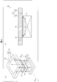
- FIG. 1A is an exploded perspective view showing the configuration of the optical element package 10 according to the present embodiment
- FIG. 1B is a cross-sectional view showing the configuration of the optical element package 10.
- FIG. 2 is a cross-sectional view taken along the line AA ′ shown in FIG.
- the optical element package 10 is obtained by sealing the optical element 11 in a housing constituted by a lid 13 and a main body 14.
- a housing constituted by a lid 13 and a main body 14.
- each of the optical element 11, the lid 13, and the main body 14 will be described.
- cover 13, and the main body 14 is demonstrated.
- LCOS Liquid Crystal On Silicon
- the optical element package 10 is expressed as LCOS package 10.
- the optical element 11 is not limited to a reflective optical element such as LCOS, and may be a light receiving optical element or a light emitting optical element.
- the light receiving type optical element include an image pickup element such as a CMOS and a light detection element such as a photodiode.
- the light emitting optical element include a light emitting diode and a laser diode (for example, VCSEL (vertical cavity surface emitting laser)).
- the LCOS 11 is configured by sequentially laminating a reflective mirror made of a metal thin film, a liquid crystal layer, and a cover glass on a silicon substrate.
- the cover glass is composed of a glass layer. Since the configuration of such an LCOS is well known, the description of the specific configuration of the LCOS 11 is omitted. Also, in FIG. 1B, the detailed configuration is not described.
- the surface on which the cover glass of LCOS 11 is formed functions as the light receiving surface 11a.
- the light receiving surface 11a of the LCOS 11 is divided into an effective area Ae that is an area with an optical function and an invalid area Aie that is an area without an optical function (see FIG. 1A).
- the effective area Ae refers to an area where a pixel electrode is formed on a silicon substrate, and is formed in the center of the light receiving surface 11a.
- the invalid area Aie is formed so as to surround the effective area Ae.
- the LCOS 11 is connected to a control board (not shown) via an FPC (flexible print base) 16.
- FPC flexible print base
- the method of connecting the LCOS 11 and the FPC 16 is not particularly limited.
- a method of connecting the FPC 16 to an electrode (not shown) formed in the invalid area Aie of the light receiving surface 11a of the LCOS 11 by wire bonding is used. be able to.
- the bonding wire may be sealed with resin.
- the electrode for connecting the bonding wire may be formed on the light receiving surface 11a of the LCOS 11 or may be formed on the back surface 11b which is the surface opposite to the light receiving surface 11a of the LCOS 11.
- the lid 13 is a lid having an optical window 13a that transmits light, and forms a casing that seals the LCOS 11 together with a main body 14 to be described later.
- the lid 13 includes an optical window 13a and an optical window frame 13b.
- the optical window 13a is constituted by a glass layer having translucency.
- the material which comprises the optical window 13a is not limited to glass, What is necessary is just the material which permeate
- the optical window frame 13b is a frame that holds the optical window 13a, and is made of metal.
- the optical window 13a and the optical window frame 13b are bonded by solder bonding capable of maintaining airtightness.
- a joining method using an adhesive, a joining method using low-melting glass, or the like can be given as another example of the joining method for joining the optical window 13a and the optical window frame 13b.
- the joining method for joining the optical window 13a and the optical window frame 13b is not limited to these joining methods, and can be appropriately selected from joining methods capable of maintaining airtightness.
- the material constituting the optical window frame 13b is preferably a metal because it can be welded to the frame 14c described later, but any material that can be closely bonded to the frame 14c may be used.
- the lid 13 includes the optical window 13a and the optical window frame 13b.
- the lid according to the embodiment of the present invention may be configured to omit the optical window frame 13b.
- the optical window 13a should just be comprised so that the outer edge can be joined with the flame
- the main body 14 includes a base substrate 14a, a plating layer 14b, and a frame 14c.
- the main body 14 forms a casing that seals the LCOS 11 together with the lid 13.
- the base substrate 14a is a member that forms the bottom of the main body 14, and is made of ceramics.
- a plating layer 14b is formed on the outer edge portion of one surface of the base substrate 14a.
- the material constituting the base substrate 14a is not limited to ceramics, and can be appropriately determined in consideration of various characteristics such as heat conduction characteristics and weight.
- the frame 14c is a member that forms the side surface of the main body 14, and is made of metal.
- the frame 14c is a cylindrical member configured by four surfaces, and the opening has a rectangular shape.
- the base substrate 14a is welded to one of the two openings of the frame 14c via the plating layer 14b.
- the height of the frame 14c is uniform everywhere. According to this configuration, it becomes easy to arrange the base substrate 14a and the optical window 13a in parallel when a base substrate 14a and an optical window 13a described later are joined to the frame 14c.
- An opening 14c1 is formed on one of the four surfaces constituting the frame 14c.
- the opening 14c1 is an opening for pulling out the FPC 16 from the inside of the main body 14 to the outside. The configuration for pulling out the FPC 16 will be described later with reference to FIG.
- the material constituting the frame 14c is preferably a metal because it can be welded to the optical window frame 13b described above, but any material that can be closely bonded to the optical window frame 13b may be used.
- the main body 14 includes a base substrate 14a, a plating layer 14b, and a frame 14c.
- the main body 14 may be configured by a single member in which the base substrate and the frame are integrally formed.
- the LCOS 11 is bonded to the lid 13 so that at least a part of the effective area Ae overlaps the optical window 13a.
- a configuration is adopted in which the LCOS 11 is bonded to the lid 13 so that the entire effective area Ae overlaps the optical window 13a.
- the lid 13 including the optical window 13a to which the LCOS 11 is bonded is joined to the other opening of the frame 14c so as to face the base substrate 14a welded to the frame 14c.
- the method for joining the lid 13 and the frame 14c may be any method that can seal the space formed by the lid 13 and the frame 14c.
- the optical window frame 13b and the frame 14c are both made of metal, the optical window frame 13b and the frame 14c are welded by seam welding.
- the FPC 16 connected to the LCOS 11 is drawn out of the LCOS package 10 through the opening 14c1.
- the opening 14c1 is filled with a sealing resin 17.
- solder may be employed instead of the sealing resin 17 as a member for sealing the opening 14c1.
- solder can be filled in the opening 14c1 by using local heating such as laser irradiation.
- the distance between the LCOS 11 and the lid 13 can be reduced as compared with the case where the LCOS 11 is placed on the bottom of the main body 14. That is, it is possible to suppress the possibility of dust entering between the LCOS 11 and the lid 13 in the space sealed by the housing. Therefore, the LCOS package 10 has an effect of suppressing the performance degradation of the LCOS 11 that may be caused by dust on the optical path of light incident on the LCOS 11 or emitted from the LCOS 11 in the LCOS package in which the LCOS 11 is sealed in the casing.
- the LCOS 11 is the adhesive layer 12 formed on the effective area Ae, and is bonded to the optical window 13a of the lid 13 via the translucent adhesive layer 12. ing. Therefore, the relative positional relationship between the LCOS 11 and the optical window 13a, for example, the distance between the LCOS 11 and the optical window 13a depends only on manufacturing errors when the LCOS 11 is bonded to the optical window 13a.
- the solid-state imaging device described in Patent Document 1 (1) the solid-state imaging element is mounted on the base substrate, (2) the resin frame is formed on the base substrate, (3 ) The transparent plate is joined to the upper end of the resin frame. That is, the base substrate and the resin frame are interposed between the solid-state imaging device and the transparent plate. For this reason, the relative positional relationship between the solid-state imaging device and the transparent plate, for example, the distance between the solid-state imaging device and the transparent plate, must be influenced by the base substrate and the resin frame.
- the distance between the solid-state imaging device and the transparent plate is the manufacturing error of the base substrate and the resin frame, the manufacturing error when the solid-state imaging device is bonded to the base substrate, and the manufacturing when the base substrate is bonded to the resin frame. Errors and manufacturing errors when the transparent plate is bonded to the resin frame are accumulated.
- the LCOS package 10 can easily achieve a uniform optical path length of light incident on the LCOS 11 or light emitted from the LCOS 11. There is an effect.
- the LCOS 11 is an adhesive layer 12 formed on the effective area Ae, and is preferably bonded to the optical window 13a via the adhesive layer 12 having translucency.
- a translucent adhesive layer is interposed between the effective area Ae and the lid 13 optical window 13a. That is, since no gap is formed between the effective area Ae and the optical window 13a, there is no room for dust to enter between the effective area Ae and the optical window 13a. Therefore, the LCOS package 10 has an effect of eliminating the performance degradation of the LCOS 11 that may be caused by dust incident on the LCOS 11 or emitted from the LCOS 11 in the LCOS package in which the LCOS 11 is sealed in the casing.
- the LCOS 11 is preferably separated from the main body 14 (see FIG. 1B). According to this configuration, since it is possible to prevent the formation of a heat conduction path via the main body 14 between the external environment and the LCOS 11, heat can flow into the optical element from the external environment, and Heat can be prevented from flowing out from the element to the external environment. Therefore, the optical element package according to one embodiment of the present invention has an effect of suppressing the influence of the temperature change in the external environment of the optical element package on the optical element.
- the material forming the adhesive layer 12 is a light-transmitting epoxy resin, silicone resin, acrylic resin, or benzoic acid. It preferably consists of cyclobutene.
- the refractive index of the material which comprises these adhesive bond layers 12 is contained in the range of 0.9 or more and 1.1 or less with respect to the refractive index of a glass layer.
- the refractive index of the material constituting the adhesive layer 12 is in the range of 0.9 to 1.1 with respect to the refractive index of the glass layer, it can occur at the interface between the adhesive layer 12 and the glass layer. Light reflection can be suppressed to a practically sufficient level. That is, the LCOS package 10 configured in this manner suppresses reflection of light that may occur at each of the interface between the optical window 13 a and the adhesive layer 12 and the interface between the adhesive layer 12 and the light receiving surface 11 a of the LCOS 11. The effect to do. As a result, it is possible to omit an antireflection film for suppressing light reflection that may occur at the interface described above.
- FIG. 2A is a flowchart showing a method for manufacturing the LCOS package 10.
- FIG. 2B is a flowchart showing details of the process of adhering the LCOS 11 to the optical window 13a in the manufacturing method shown in FIG.
- the LCOS package 10 employs a configuration in which the LCOS 11 is bonded to the optical window 13a via the adhesive layer 12 formed on the effective area Ae.
- the manufacturing method of the LCOS package 10 includes a bonding step (step S12) in which the LCOS 11 is bonded to the lid 13 and a lid 13 to which the LCOS 11 is bonded, as shown in FIG. And a sealing step (step S13) for sealing the LCOS 11 by joining the main body 14 to each other.
- the lid 13 is formed by bonding the optical window 13a to the optical window frame 13b.
- step S12 the LCOS 11 is bonded to the optical window 13a through the adhesive layer 12 formed on the effective area Ae. Note that the FPC 16 is connected to the LCOS 11 in advance.
- step S13 the optical window frame 13b to which the LCOS 11 is bonded is welded to the frame 14c. Prior to this welding, the FPC 16 is pulled out of the main body 14 from the opening 14c1. After the optical window frame 13b and the frame 14c are welded, the sealing resin 17 is filled into the opening 14c1 from which the FPC 16 is drawn. Through the above steps, the LCOS package 10 is manufactured.
- steps S12 to S13 are performed in a clean environment (for example, a clean room) having a function of removing dust floating in the air.
- step S12 is preferably performed in a clean environment.
- step S12 By performing at least step S12 in a clean environment, it is possible to greatly suppress the possibility of dust being mixed into the adhesive layer 12. That is, it is possible to greatly suppress the possibility of dust entering the optical path of the LCOS 11.
- step S13 for welding the optical window frame 13b and the frame 14c the sealing resin 17 may be filled in the opening 14c1 from which the FPC 16 is drawn, and step S13 may be performed under vacuum.
- the welding of the optical window frame 13b and the frame 14c in step S13 is welding that can be hermetically sealed.
- step S13 when welding capable of hermetically sealing is employed, step S13 is preferably performed in a nitrogen atmosphere, a helium atmosphere, a mixed atmosphere of helium and nitrogen, or the like.
- step S13 By executing step S13 in a nitrogen atmosphere, it is possible to prevent the nitrogen gas from being filled in the space hermetically sealed by the lid 13 and the main body 14 and mixing moisture. Therefore, it is possible to prevent the LCOS 11 from being deteriorated by moisture mixed therein.
- Step S13 by executing Step S13 in a helium atmosphere or a mixed atmosphere of helium and nitrogen, helium gas is introduced into the space hermetically sealed by the lid 13 and the main body 14. If there is a problem with the airtightness of the LCOS package 10, helium gas leaks from the space. Therefore, the helium leak detector can be used to check the tightness of the LCOS package 10.
- step S13 may be executed under vacuum.
- step S13 By executing step S13 under vacuum, the space formed by the lid 13 and the main body 14 is in a vacuum state. According to this configuration, since a vacuum layer is formed between the LCOS 11 and the main body 14, the LCOS package 10 has an effect of further suppressing the influence of the temperature change of the external environment on the LCOS 11.
- step S12 the step of adhering the LCOS 11 to the optical window 13a (step S12) will be described in detail (see FIG. 2B).
- step S121 an adhesive is applied to the optical window 13a.
- the area where the adhesive is applied is an area that overlaps the effective area Ae when the LCOS 11 and the optical window 13a are bonded.
- step S122 the LCOS 11 is placed on the optical window 13a so that the area where the adhesive is applied to the optical window 13a matches the effective area Ae.
- step S123 the LCOS 11 placed on the optical window 13a is pressurized.
- the thickness of the adhesive applied to the optical window 13a becomes uniform, and the light receiving surface 11a of the LCOS 11 and the surface of the optical window 13a facing the LCOS 11 can be bonded in a parallel state.
- step S124 the adhesive applied to the optical window 13a is heated and cured by heating the optical window 13a on which the LCOS 11 is placed using an oven. Through this step, the adhesive applied to the optical window 13a becomes the adhesive layer 12 interposed between the optical window 13a and the LCOS.
- step S124 when the adhesive applied to the optical window 13a is heat-cured, the pressure in the oven is preferably set to a vacuum.
- the adhesive By heat-curing the adhesive in a vacuum state, the adhesive can be heat-cured while eliminating bubbles that may be generated in the adhesive (while defoaming).
- bubbles When bubbles remain in the adhesive layer 12, the bubbles may obstruct the optical path of light incident on the effective area Ae or light emitted from the effective area Ae.
- By heating and curing the adhesive while defoaming there is an effect of suppressing the possibility of bubbles remaining in the adhesive layer 12.
- step S124 the LCOS 11 placed on the optical window 13a may be continuously pressurized.
- the adhesive By heating and curing the adhesive while applying pressure to the LCOS 11, there is an effect of suppressing the possibility that the thickness of the adhesive layer 12 is not uniform during the heat curing.
- step S123 may be omitted when a configuration in which a spacer is interposed between the LCOS 11 and the optical window 13a is employed.
- step S121 instead of applying the adhesive to the optical window 13a, a configuration in which the adhesive is applied to the effective area Ae of the LCOS 11 may be adopted.
- FIG. 3A is an exploded perspective view showing the configuration of the LCOS package 20 according to the first modification
- FIG. 3B is a cross-sectional view showing the configuration of the LCOS package 20
- FIG. FIG. 6 is a cross-sectional view taken along the line AA ′ shown in FIG.
- the LCOS package 20 is different from the LCOS package 10 in that it further includes a spacer 21 interposed between the LCOS 11 and the optical window 13a. Therefore, in this modification, the spacer 21 will be described.
- symbol is attached
- 3A and 3B the main body 14 and the FPC 16 which are the same as those of the LCOS package 10 are omitted and not shown.
- the spacer 21 is a spacer disposed between the LCOS 11 and the optical window 13a, and a light receiving surface 11a that is a surface facing the optical window 13a of the LCOS 11 and a surface that faces the LCOS 11 of the optical window 13a are parallel to each other. It is a spacer to keep.
- the spacer 21 is an annular spacer formed so as to surround the effective area Ae. That is, the spacer 21 is disposed on the invalid area Aie. Therefore, regardless of whether or not the spacer 21 is made of a light-transmitting material, the spacer 21 does not hinder the optical path of light incident on the effective area Ae or light emitted from the effective area Ae.
- each of the three or more protrusions having a common height may be an independent member or connected by an annular connecting member.
- shape of each projection part is not limited, For example, cones, such as a cone and a pyramid, may be sufficient as a cylinder and a prism.
- FIG. 4 is a cross-sectional view showing the configuration of the LCOS package 30 according to the second modification.
- the LCOS package 30 is different from the LCOS package 10 in that a heater 31 is provided. Therefore, in this modification, the heater 31 will be described.
- symbol is attached
- the heater 31 is attached to a surface opposite to the surface on which the effective area Ae of the LCOS 11 is formed, and the LCOS 11 and the heater 31 are separated from the main body 14. Each terminal provided in the heater 31 is connected to the FPC 16.
- the heater 31 is a ceramic heater, but is not limited thereto.
- LCOS 11 Since LCOS 11 includes a liquid crystal layer, it has a preferable temperature range as an operating temperature. Since the heater 31 is attached, the LCOS package 30 can raise the temperature of the LCOS 11 and can raise the temperature of the LCOS 11 to a preferable temperature range as the operating temperature.
- the LCOS 11 and the heater 31 are separated from the main body 14, it is possible to prevent a heat conduction path through the main body 14 from being formed between the external environment of the LCOS package 30 and the heater 31. Therefore, the LCOS package 30 can suppress heat from flowing into the heater from the external environment, and heat generated by the heater from flowing out to the external environment. Therefore, the LCOS package 30 has an effect of reducing the power consumption of the heater.
- the heater 31 may include a temperature sensor that detects the temperature of the LCOS 11.
- the LCOS package 30 can control the temperature of the LCOS 11 within the preferable temperature range as the operating temperature by feedback control.
- the LCOS package 30 can suppress the influence of the temperature change of the external environment on the LCOS 11 and the heater 31. Therefore, the LCOS package 30 configured as described above has an effect of improving the stability of temperature control by the heater 31.
- FIG. 3A is a cross-sectional view showing a configuration of the LCOS package 40 according to the third modification
- FIG. 3B is a cross-section showing a configuration of the LCOS package 50 according to the fourth modification
- FIG. 3C is a cross-sectional view showing a configuration of the LCOS package 60 according to the fifth modification
- FIG. 3D is an illustration of the LCOS package 70 according to the sixth modification. It is sectional drawing which shows a structure.
- the LCOS packages 40 to 70 are different from the LCOS package 10 in the manner of joining the LCOS 11 and the window 13. Therefore, in the third to sixth modifications, a mode in which the LCOS 11 and the window 13 are joined will be described.
- symbol is attached
- 5A to 5D the main body 14 and the FPC 16 which are the same as those of the LCOS package 10 are omitted and not shown.
- the LCOS package 40 employs a double-sided tape 42 instead of the adhesive layer 12.
- the LCOS 11 of the LCOS package 40 is a double-sided tape formed on the effective area Ae, and is bonded to the lid 13 and more specifically to the optical window 13a via a light-transmitting double-sided tape. ing.
- the optical window 13a of the LCOS 11 is compared with the case where the double-sided tape is not interposed between the LCOS 11 and the optical window 13a. It becomes easy to keep the facing surface and the surface facing the LCOS 11 of the optical window 13a in parallel. In other words, it becomes easy to keep the distance between the light receiving surface 11a of the LCOS 11 and the surface of the optical window 13a facing the LCOS 11 constant. Thereby, the optical path length of the light incident on the LCOS 11 or the light emitted from the LCOS 11 becomes uniform regardless of the incident position or the emission position. Therefore, there is an effect of improving the operation accuracy of the LCOS 11.
- the LCOS package 40 has an effect of suppressing reflection of light that can occur at each of the interface between the optical window 13a and the double-sided tape 42 and the interface between the double-sided tape 42 and the light receiving surface of the LCOS 11.
- the LCOS 11 of the LCOS package 50 is (1) an adhesive layer 52a formed so as to cover the effective area Ae, and an adhesive layer 52a having translucency, and (2) It is joined to the lid 13 and more specifically to the optical window 13a through both of the adhesive layer 52b formed in the invalid area Aie surrounding the effective area Ae.
- the adhesive layer 52 a is an adhesive layer corresponding to the adhesive layer 12 of the LCOS package 10.
- the LCOS package 50 has an effect of increasing the adhesive strength between the LCOS 11 and the lid 13.
- the adhesive layer 52a is preferably formed so as to protrude beyond a region that is slightly larger than the effective region Ae.
- the width of the adhesive layer 52a that protrudes from the effective region Ae is the thickness t of the adhesive layer 52a and the incident It is preferable that the incident angle ⁇ of light exceeds t ⁇ tan ⁇ . According to this structure, it can suppress that the incident light which injects into the outer edge part of the effective area
- the LCOS 11 of the LCOS package 60 is formed on the ineffective area Aie that surrounds the effective area Ae via the lid 13 via an annular adhesive layer 62 that surrounds the effective area Ae. Specifically, it is joined to the optical window 13a. That is, a gap is formed between the effective area Ae and the optical window 13a.
- the gap formed between the effective area Ae and the optical window 13a has a height equivalent to the thickness of the adhesive layer 62.
- step S13 shown in FIG. 2A is performed in the atmosphere, the gap is filled with air.
- the thermal conductivity of the void that is, the thermal conductivity of air, is lower than the thermal conductivity of the adhesive layer 12. Therefore, the LCOS package 60 has an effect of suppressing the influence of the temperature change of the external environment on the effective area Ae of the LCOS 11 as compared with the LCOS package 10.
- step S13 When manufacturing the LCOS package 60, it is preferable to perform step S13 in a vacuum. In this case, it is preferable that the welding between the optical window frame 13b and the main body 14 in step S13 is a hermetically sealable weld. According to this step S13, the gap formed between the effective area Ae and the optical window 13a can be evacuated. Since the thermal conductivity of the vacuum is lower than the thermal conductivity of air, the influence of the temperature change of the external environment on the effective region Ae of the LCOS 11 can be further suppressed.
- the gap formed between the effective area Ae and the optical window 13a is surrounded by the adhesive layer 62. Therefore, the LCOS package 60 can prevent dust from entering the gap. Therefore, the LCOS package 60 has an effect of preventing the degradation of the performance of the optical element that may be caused by dust on the optical path of the light incident on the LCOS 11 or emitted from the LCOS 11 in the LCOS package in which the LCOS 11 is sealed in the casing. .
- the adhesive layer 62 may be formed only in a part of an annular region surrounding the effective region Ae.
- the adhesive layer 62 may be formed only at the four corners of the invalid area Aie in the annular area so as to bond the four corners of the invalid area Aie.
- the height of the adhesive layer 62 is equal to the thickness of the adhesive layer 62 as described above, and the height of the gap formed between the solid-state imaging device and the transparent plate in the solid-state imaging device described in Patent Document 1. Low compared to Therefore, even if it is the LCOS package 60 comprised in this way, possibility that dust will penetrate
- the LCOS package 60 has an effect of suppressing a decrease in performance of an optical element that may be caused by dust on an optical path of light incident on the LCOS 11 or emitted from the LCOS 11 in the LCOS package in which the LCOS 11 is sealed in a casing. .
- the adhesive layer 62 is formed on a region excluding the region near the effective region Ae in the invalid region Aie.
- the area near the effective area Ae is an annular area surrounding the effective area Ae, and the width of the annular portion is t ⁇ tan ⁇ or more as the thickness t of the adhesive layer 62 and the incident angle ⁇ of incident light. It is. According to this configuration, it is possible to suppress the incident light incident on the outer edge portion of the effective area Ae from being blocked by the adhesive layer 62.
- the adhesive layer formed on the invalid area Aie is employed as in the LCOS package 60
- the adhesive layer is formed on the invalid area Aie of the LCOS 11 as in the LCOS package 70 illustrated in FIG.
- the LCOS package 70 has the same effect as the LCOS package 60.
- LCOS package 70 a configuration in which the LCOS package 70 is bonded to the optical window 73a and the optical window frame 73b of the lid 73 via the adhesive layer 72 formed on the invalid area Aie of the LCOS 11 may be adopted.
- an adhesive containing a filler may be used to form the adhesive layers 52b, 62, and 72 formed on the ineffective area Aie.
- the adhesive layer composed of the adhesive containing the filler can achieve higher adhesive strength than the adhesive layer composed of the adhesive not containing the filler. Therefore, the LCOS packages 50, 60, 70 configured as described above have an effect of further increasing the adhesive strength between the LCOS 11 and the lid 13. By increasing the adhesive strength between the LCOS 11 and the lid 13, it is possible to improve the impact resistance and durability of the LCOS package.
- FIG. 6 is a cross-sectional view showing a configuration of an LCOS package 80 according to a seventh modification.
- the LCOS package 80 is different from the LCOS package 10 in the configuration for drawing out the wiring connecting the LCOS 11 and the control board to the outside of the casing. Therefore, in this modification, a configuration for drawing the wiring connecting the LCOS 11 and the control board to the outside of the housing will be described.
- symbol is attached
- the LCOS package 80 includes a housing 84 instead of the main body 14 of the LCOS package 10.
- the housing 84 includes a base substrate 84a, a plating layer 84b, and a frame 84c.
- Each of the base substrate 84a, the plating layer 84b, and the frame 84c is a member corresponding to the base substrate 14a, the plating layer 14b, and the frame 14c of the LCOS package 10.
- the base substrate 84a is a multilayer ceramic substrate formed by laminating a plurality of ceramic substrates (ceramic substrates).
- the connector 81 is disposed on the surface of the base substrate 84a located on the inner side of the housing 84, and on the surface of the base substrate 84a located on the outer side of the housing 84, A connector 82 is disposed.
- the connector 81 and the connector 82 are electrically connected by a conductive path 84a1 formed in the base substrate 84a.
- the conductive path 84a1 is a conductive film formed on the surface of the ceramic substrate located in the intermediate layer of the base substrate 84a and a via formed along the thickness direction of the base substrate 84a. Each of the vias is formed. These vias are exposed on the surface of the base substrate 84a and are configured to be electrically connected to the conductive film formed in the intermediate layer of the base substrate 84a. Therefore, the connector 81 connected to one via and the connector 82 connected to the other via are electrically connected to each other.
- the FPC 16 connects the LCOS 11 and the connector 81. One end of the FPC 85 is connected to the connector 82.
- the LCOS 11 can be connected to the control board by connecting the other end of the FPC 85 to the control board.
- the opening 14c1 is formed in the main body 14 in advance, the FPC 16 is pulled out from the opening 14c1, and the opening 14c1 from which the FPC 16 is pulled out is sealed with the sealing resin 17. Can be omitted.
- FIG. 7 is a cross-sectional view showing a configuration of an LCOS package 90 according to an eighth modification.
- the LCOS package 90 is different from the LCOS package 80 in the configuration for drawing out the wiring connecting the LCOS 11 and the control board to the outside of the housing. Therefore, in this modification, a configuration for drawing the wiring connecting the LCOS 91 and the control board to the outside of the housing will be described.
- symbol is attached
- the LCOS package 90 includes a casing 94 instead of the casing 84 of the LCOS package 80.
- An electrode 95 made of a conductive film is formed on the back surface of the LCOS 91.
- the housing 94 includes a first base substrate 94a, a plated layer 94b, a frame 94c, a second base substrate 94d, a conductive path 94e, a pad 94f, a plated layer 94g, and a plated layer 94h. It is obtained by deforming the housing 84 provided.
- the first base substrate 94a and the frame 94c are welded via a plating layer 94b.
- the second base substrate 94d and the frame 94c are welded via a plating layer 94g.
- the second base substrate 94d and the optical window frame 13b are welded via a plating layer 94h.
- the LCOS package 90 configured as described above can seal the LCOS 91 inside the space formed by the casing 94 and the lid 13.
- a pad 94f made of a conductive film is formed on a surface of the second base substrate 94d that faces the first base substrate 94a and is located inside the housing 94.
- a connector 97 is disposed on the surface located at the position.
- the pad 94f and the connector 97 are electrically connected by a conductive path 94e formed in the second base substrate 94d.
- the conductive path 94e is configured similarly to the conductive path 84a1 formed in the base substrate 84a. Therefore, the pad 94f and the connector 97 are electrically connected to each other.
- connection 96 is a wiring formed by wire bonding the electrode 95 and the pad 94f. That is, the connection 96 electrically connects the electrode 95 and the pad 94f.
- One end of the FPC 98 is connected to the connector 97. By connecting the other end of the FPC 98 to the control board, the LCOS 91 can be connected to the control board.
- the LCOS 91 and the conductive path 94e can be electrically connected by the connection 96 using wire bonding.
- the LCOS package 90 can omit the FPC 16 and the connector 81 when compared with the LCOS package 80, and can simplify the manufacturing process.
- FIG. 8 is a cross-sectional view showing the configuration of the optical switch 100 according to the present embodiment.
- the optical switch 100 includes the LCOS package 10 according to the first embodiment.
- the LCOS package included in the optical switch 100 is not limited to the LCOS package 10 and may be any of the LCOS packages 20 to 90 according to the modifications of the present invention.
- the optical switch 100 includes a casing 101, an optical system 103 configured inside the casing 101, and an LCOS package 10.
- the configuration of the casing 101 and the manner of joining the casing 101 and the LCOS package 10 will be described, and then the configuration of the optical system 103 will be described.
- the housing 101 is a housing for housing the optical system 103 therein.
- the housing 101 is provided with an opening for optically coupling the optical system 103 and the LCOS package 10.
- casing 101 is not specifically limited, For example, a metal, resin, etc. are employable.
- the LCOS package 10 is bonded so that the optical window 13a of the lid 13 overlaps with the opening of the housing 101, and the light incident surface of the optical window 13a and the surface of the housing 101 surrounding the opening are parallel to each other. It is joined to the housing 101 via a member.
- the optical window frame 13b and the housing 101 are bonded via an adhesive layer 102 that is a bonding member. According to this configuration, the light incident surface of the optical window 13 a and the surface of the housing 101 surrounding the opening are kept parallel by the adhesive layer 102.
- the optical window frame 13b of the lid 13 may be joined to the housing 101 using a bolt as a joining member. Between the optical window frame 13b and the housing 101, there is a spacer (not shown in FIG. 8) that keeps the surfaces of the optical window 13a and the optical window 107 facing each other in parallel.
- the reference surface for joining the LCOS package 10 to the housing 101 is not the surface of the main body 14 of the LCOS package 10, but the surface of the optical window 13a, A surface facing the window 107 is employed.
- the light receiving surface of the LCOS 11 and one surface of the optical window 13a are parallel, and the other surface of the optical window 13a and the surface of the optical window 107 facing the optical window 13a are parallel. Therefore, it is easier to keep the light receiving surface of the LCOS 11 and the surface of the optical window 107 facing the optical window 13a parallel to each other than when any surface of the main body 14 is used as a reference surface. Therefore, even when the position of the light incident on the light receiving surface of the LCOS 11 changes, there is an effect that the variation in the optical path length can be easily suppressed.
- the optical system 103 includes an input port 109, an output port 110, a microlens array 111, a dispersion unit 113, a condensing element 115, a mirror 117, and an optical bench 119.
- Each of the input port 109, the output port 110, the microlens array 111, the dispersion unit 113, the condensing element 115, and the mirror 117 is fixed on a light-transmitting glass optical table 119.
- the input port 109 is a port for inputting wavelength-multiplexed light to the optical switch 100 as input light.
- the output port 110 is a port that outputs output light, which is light whose path is switched by the LCOS 11 of the LCOS package 10, from the optical switch 100.
- the input port 109 and the output port 110 are configured by optical fibers.
- FIG. 8 shows only one input port 109 and two output ports 110 in the port array configured as described above.
- microlenses corresponding to each of the input port 109 and the output port 110 constituting the port array are arranged in an array.
- the microlens array 111 converts the input light input from the input port 109 to the optical switch 100 into a parallel light beam, and focuses the output light whose path is switched by the LCOS 11 on the output port 110.
- the dispersion unit 113 is for dispersing the input light converted into a parallel light beam by the microlens array 111 for each wavelength.
- a transmissive dispersion element can be employed.
- a reflection type diffraction grating may be adopted as the dispersion unit 113.
- the configuration of the optical system 103 may be modified to a configuration suitable for the reflection type diffraction grating.
- the condensing element 115 condenses the light dispersed for each wavelength by the dispersion unit 113, and is, for example, a convex lens.
- the mirror 117 guides the input light collected by the light condensing element 115 in the direction of the LCOS 11 of the LCOS package 10 and guides the output light whose path is switched by the LCOS 11 in the direction of the output port 110. is there.
- Input light is incident on the LCOS 11 of the LCOS package 10 from the optical system 103 configured as described above.
- the LCOS 11 switches the optical path of the input light input from the optical system 103 by controlling the alignment state of the liquid crystal layer, and outputs the output light to the optical system 103 by reflecting the input light.
- the optical switch 100 configured as described above disperses the input light input from the input port 109 according to the wavelength, and switches the optical path of the light having the desired wavelength, thereby allowing the light having the desired wavelength to be switched. It can be output to any output port 110 as output light.
- the optical element package according to the first embodiment described above is an optical element package in which an optical element is sealed in a housing, and includes a lid having an optical window that transmits light. The region is joined to the lid so that at least a part of the region overlaps the optical window.
- the optical element package having the above configuration is an optical element that can be generated by dust on an optical path of light incident on or emitted from the optical element in the optical element package in which the optical element is sealed in a housing. There is an effect of suppressing the performance degradation.
- the cause of the error related to the relative positional relationship between the optical element and the optical window (for example, the distance between the optical element and the optical window) is This is only a manufacturing error when the optical element is bonded to the lid. Therefore, according to the above configuration, it is easier than the solid-state imaging device described in Patent Document 1 to make the optical path length of the light incident on the optical element or the light emitted from the optical element uniform.
- the optical element is preferably bonded to the lid via a translucent adhesive layer formed on the effective area.
- the translucent adhesive layer is interposed between the effective area and the lid of the optical element, more specifically, between the effective area and the optical window. That is, since no gap is formed between the effective area and the optical window, there is no room for dust to enter between the effective area and the optical window. Therefore, the optical element package having the above-described configuration has an effect of eliminating the deterioration in performance of the optical element that may be caused by dust on the optical path of light that enters or exits the optical element.
- the optical element is formed on a translucent adhesive layer formed on the effective area and an ineffective area surrounding the effective area. It is preferable to be joined to the lid through both of the adhesive layers.
- the optical element package having the above configuration has an effect of increasing the adhesive strength between the optical element and the lid.
- the surface of the effective area and the optical window are made of a glass layer
- the adhesive layer formed on the effective area is made of epoxy resin, silicone. It is preferably made of a resin, an acrylic resin, or benzocyclobutene.
- the refractive index of the adhesive layer is approximately the same as the refractive index of the surface of the effective area of the optical element and the refractive index of the optical window. Therefore, the optical element package having the above-described configuration has an effect of suppressing reflection of light that can occur at each of the interface between the optical window and the adhesive layer and the interface between the adhesive layer and the light receiving surface of the optical element. .
- the optical element is bonded to the lid via an adhesive layer formed on an ineffective area surrounding the effective area, and the effective area and the It is preferable that a gap is formed between the optical window.
- the optical element package having the above configuration has an effect of suppressing the influence of the temperature change of the external environment of the optical element package on the effective region.
- the adhesive layer formed on the invalid region is composed of an adhesive containing a filler.
- the adhesive layer containing the filler can realize high adhesive strength as compared with the adhesive layer not containing the filler. Therefore, according to said structure, there exists an effect which raises the adhesive strength of an optical element and a lid
- the optical element package according to the first embodiment described above is a spacer interposed between the optical element and the optical window, the surface of the optical element facing the optical window, and the optical of the optical window. It is preferable to further include a spacer that keeps the surface facing the element parallel.
- the surface of the optical element that faces the optical window and the surface of the optical window that faces the optical element can be easily kept parallel.
- the optical path length of the light incident on the optical element or the light emitted from the optical element becomes uniform regardless of the incident position or the emission position. Therefore, there is an effect of increasing the operation accuracy of the optical element.
- the optical element is bonded to the lid via a translucent double-sided tape formed on the effective area.
- the double-sided tape is interposed between the optical element and the optical window. Therefore, the optical element package having the above configuration faces the optical element of the optical window and the optical element of the optical window as compared with the case where the double-sided tape is not interposed between the optical element and the optical window. It becomes easy to keep the surface parallel. As a result, the optical path length of the light incident on the optical element or the light emitted from the optical element becomes uniform regardless of the incident position or the emission position. Therefore, there is an effect of increasing the operation accuracy of the optical element.
- the optical element package according to the first embodiment described above further includes a main body that forms a casing together with the lid, and the optical element is separated from the main body.
- the optical element package having the above configuration since it is possible to prevent the formation of a heat conduction path through the main body between the external environment of the optical element package and the optical element, heat is transmitted from the external environment to the optical element through the main body. It is possible to suppress inflow and heat outflow from the optical element to the external environment through the main body. Therefore, the optical element package having the above configuration has an effect of suppressing the influence of the temperature change of the external environment on the optical element.
- a heater is attached to the surface of the optical element opposite to the surface on which the effective area is formed.
- the optical element and the heater are It is preferable that it is separated from the main body.
- the optical element has a preferable temperature range as the operating temperature (for example, when the optical element is an LCOS element)
- the temperature of the optical element is increased to the preferable temperature range by using the heater. Can be made.
- the optical switch according to the second embodiment described above preferably includes any one of the optical element packages according to the first embodiment described above.
- the optical switch according to the second embodiment has the same effect as the optical element package according to the first embodiment.
- the method for manufacturing an optical element package according to the first embodiment described above is a method for manufacturing an optical element package in which an optical element is sealed in a housing constituted by a lid having an optical window that transmits light and a main body.
- the method for manufacturing the optical element package according to the first embodiment described above has the same effects as those of the optical element package according to the first embodiment described above.
- the present invention can be used for an optical element package in which an optical element is sealed in a casing.
- LCOS package (optical element package) 11,91 LCOS (optical element) 11a Light-receiving surface 11b Back surface 12, 52a, 52b, 62, 72 Adhesive layer 13, 73 Lid 13a, 73a Optical window 13b, 73b Optical window frame 14, 84, 94 Main body 14a, 84a Base substrate 14b, 84b, 94b, 94g 94h Plating layer 14c, 84c, 94c Frame 81, 82, 97 Connector 16, 85, 98 FPC 17 Sealing resin 21 Spacer 31 Heater 42 Double-sided tape 94a First base substrate 94d Second base substrate 95 Electrode 96 Connection
Landscapes
- Physics & Mathematics (AREA)
- Nonlinear Science (AREA)
- Optics & Photonics (AREA)
- General Physics & Mathematics (AREA)
- Crystallography & Structural Chemistry (AREA)
- Chemical & Material Sciences (AREA)
- Mathematical Physics (AREA)
- Engineering & Computer Science (AREA)
- Microelectronics & Electronic Packaging (AREA)
- Manufacturing & Machinery (AREA)
- Solid State Image Pick-Up Elements (AREA)
- Transforming Light Signals Into Electric Signals (AREA)
- Liquid Crystal (AREA)
Abstract
光学素子パッケージにおいて、光路上のダストによって生じ得る光学素子の性能低下を抑制する。筐体(13,14)内に光学素子(11)を封止した光学素子パッケージ(10)において、光を透過する光学窓(13a)を有する蓋(13)を備え、光学素子(11)は、光学素子(11)の有効領域(Ae)の少なくとも一部が光学窓(13a)と重なるように、蓋(13)に接合されている。
Description
本発明は、筐体内に光学素子を封止した光学素子パッケージに関する。
筐体内に各種光学素子を封止した光学素子パッケージが知られている。
特許文献1には、ベース基板、樹脂枠、及び透明板により構成された筐体内に、透明板を透過した光を受光する固体撮像素子を封止した固体撮像装置が記載されている。この固体撮像装置において、固体撮像素子は、ベース基板の上面に載置されている。
このように筐体内に固体撮像素子を封止した固体撮像装置においては、封止前に筐体内に混入した、又は、封止後に筐体内で発生したダストが、固体撮像装置の光学性能を低下させる可能性がある。例えば、これらのダストが固体撮像素子の受光面又は透明板に付着した場合、これらのダストにより固定撮像素子が受光する光の光路が遮られるので、固体撮像装置の光学性能が低下する。
筐体内におけるダストの発生を防止するための技術として、特許文献2には、ベース及び封止ガラスにより構成された筐体内にチップを封止した気密封止型半導体装置が記載されている。この気密封止型半導体装置において、チップは、ベースに形成されたキャビティー(筐体内)の底に配置され、光透過性樹脂層に埋設されている。
特許文献2に記載の気密封止型半導体装置であっても、光透過性樹脂を充填する前(例えばワイヤボンディング時)に、筐体内にダストが混入する可能性を否定できない。
これらのダストが筐体内に存在した状態で光透過性樹脂層を筐体内に充填すると、これらのダストが充填された光透過性樹脂とともに移動する可能性がある。すなわち、これらのダストが形成された光透過性樹脂層内に取り込まれ、チップに入射する、又は、チップから出射する光の光路を遮る懸念がある。
本発明は、上記の課題に鑑みてなされたものであり、その目的は、筐体内に光学素子を封止した光学素子パッケージにおいて、光学素子に入射する、又は、光学素子から出射する光の光路上のダストによって生じ得る光学素子の性能低下を抑制することにある。
上記の課題を解決するために、本発明の一態様に係る光学素子パッケージは、筐体内に光学素子を封止した光学素子パッケージにおいて、光を透過する光学窓を有する蓋を備え、上記光学素子は、当該光学素子の有効領域の少なくとも一部が上記光学窓と重なるように、上記蓋に接合されている、ことを特徴とする。
上記の構成によれば、光学素子が筐体の底に載置されている場合と比較して、光学素子と蓋との間隔を狭くすることができる。すなわち、筐体により封止された空間において、光学素子と蓋との間に、ダストが侵入する可能性を抑制することができる。したがって、本発明に係る光学素子パッケージは、筐体内に光学素子を封止した光学素子パッケージにおいて、光学素子に入射する、又は、光学素子から出射する光の光路上のダストによって生じ得る光学素子の性能低下を抑制する効果を奏する。
特許文献1に記載された固体撮像装置の場合、固体撮像素子と透明板との間にベース基板と樹脂枠とが介在する。したがって、固体撮像素子と透明板との相対的な位置関係(例えば、固体撮像素子と透明板との距離)に関する誤差は、固体撮像素子をベース基板に接合する際の誤差、ベース基板に樹脂枠を接合する際の誤差、及び、樹脂枠に透明板を接合する際の誤差が累積したものとなる。一方、上記の構成によれば、光学素子が蓋に接合されているため、光学素子と光学窓との相対的な位置関係(例えば、光学素子と光学窓との距離)に関する誤差の原因は、光学素子を蓋に接合する際の製造誤差のみである。したがって、上記の構成によれば、光学素子に入射する光又は光学素子から出射する光の光路長の均一化を図ることが、特許文献1に記載の固体撮像装置よりも容易になる。
上記の課題を解決するために、本発明の一態様に係る光学素子パッケージの製造方法は、光を透過する光学窓を有する蓋と、本体とによって構成された筐体内に光学素子を封止した光学素子パッケージの製造方法であって、上記光学素子の有効領域の少なくとも一部が上記光学窓と重なるように、当該光学素子を上記蓋に接合する接合工程と、上記光学素子が接合された上記蓋と上記筐体とを接合することによって上記光学素子を封止する封止工程と、を含んでいる、ことを特徴とする。
上記の構成によれば、本発明の一態様に係る光学素子パッケージの製造方法は、本発明の一態様に係る光学素子パッケージと同様の効果を奏する。
本発明は、筐体内に光学素子を封止した光学素子パッケージにおいて、光学素子に入射する、又は、光学素子から出射する光の光路上のダストによって生じ得る光学素子の性能低下を抑制する効果を奏する。
〔第1の実施形態〕
本発明の第1の実施形態に係る光学素子パッケージについて、図1を参照して説明する。図1の(a)は、本実施形態に係る光学素子パッケージ10の構成を示す分解斜視図であり、図1の(b)は、光学素子パッケージ10の構成を示す断面図であって、図1の(a)に示したA-A’線に沿った断面の断面図である。
本発明の第1の実施形態に係る光学素子パッケージについて、図1を参照して説明する。図1の(a)は、本実施形態に係る光学素子パッケージ10の構成を示す分解斜視図であり、図1の(b)は、光学素子パッケージ10の構成を示す断面図であって、図1の(a)に示したA-A’線に沿った断面の断面図である。
(光学素子パッケージ10の構成)
図1に示すように、光学素子パッケージ10は、蓋13と本体14とにより構成された筐体内に光学素子11を封止したものである。以下、光学素子11、蓋13、及び本体14の各々について説明する。その後に、光学素子11、蓋13、及び本体14の各々を接合する態様について説明する。
図1に示すように、光学素子パッケージ10は、蓋13と本体14とにより構成された筐体内に光学素子11を封止したものである。以下、光学素子11、蓋13、及び本体14の各々について説明する。その後に、光学素子11、蓋13、及び本体14の各々を接合する態様について説明する。
(光学素子)
本実施形態では、光学素子11の一例として、反射型液晶パネルであるLCOS(Liquid Crystal On Silicon)を採用している。したがって、本明細書では、光学素子11のことをLCOS11と表記し、光学素子パッケージ10のことをLCOSパッケージ10と表記する。なお、光学素子11は、LCOSのような反射型の光学素子に限定されるものではなく、受光型の光学素子であってもよいし、発光型の光学素子であってもよい。受光型の光学素子の例としては、CMOSなどの撮像素子、フォトダイオードなどの光検出素子などが挙げられる。発光型の光学素子の例としては、発光ダイオードやレーザーダイオード(例えば、VCSEL(垂直共振器面発光レーザー))などが挙げられる。
本実施形態では、光学素子11の一例として、反射型液晶パネルであるLCOS(Liquid Crystal On Silicon)を採用している。したがって、本明細書では、光学素子11のことをLCOS11と表記し、光学素子パッケージ10のことをLCOSパッケージ10と表記する。なお、光学素子11は、LCOSのような反射型の光学素子に限定されるものではなく、受光型の光学素子であってもよいし、発光型の光学素子であってもよい。受光型の光学素子の例としては、CMOSなどの撮像素子、フォトダイオードなどの光検出素子などが挙げられる。発光型の光学素子の例としては、発光ダイオードやレーザーダイオード(例えば、VCSEL(垂直共振器面発光レーザー))などが挙げられる。
LCOS11は、シリコン基板の上に、金属薄膜からなる反射ミラー、液晶層、及びカバーガラスを順次積層することによって構成されている。カバーガラスは、ガラス層により構成されている。このようなLCOSの構成は周知であるため、LCOS11の具体的な構成についての説明を省略する。また、図1の(b)においても、その詳細な構成を記載していない。
LCOS11のカバーガラスが形成されている面は、受光面11aとして機能する。LCOS11の受光面11aは、光学的な機能を伴う領域である有効領域Aeと、光学的な機能を伴わない領域である無効領域Aieとに二分されている(図1の(a)参照)。LCOS11において、有効領域Aeは、シリコン基板上に画素電極が形成されている領域のことを指し、受光面11aの中央に形成されている。一方、無効領域Aieは、有効領域Aeを取り囲むように形成されている。
本実施形態において、LCOS11は、FPC(フレキシブルプリント基)16を介して制御基板(不図示)に接続される。
LCOS11とFPC16とを接続する方法は、特に限定されるものではないが、例えば、LCOS11の受光面11aの無効領域Aieに形成された電極(不図示)にFPC16をワイヤボンディングにより接続する方法を用いることができる。この場合、ボンディングワイヤは、樹脂により封止してもよい。また、ボンディングワイヤを接続するための電極は、LCOS11の受光面11aに形成されていてもよいし、LCOS11の受光面11aと反対側の面である背面11bに形成されていてもよい。
(蓋)
蓋13は、光を透過する光学窓13aを有する蓋であり、後述する本体14とともにLCOS11を封止する筐体を形成する。本実施形態において、蓋13は、光学窓13a及び光学窓枠13bを備えている。
蓋13は、光を透過する光学窓13aを有する蓋であり、後述する本体14とともにLCOS11を封止する筐体を形成する。本実施形態において、蓋13は、光学窓13a及び光学窓枠13bを備えている。
光学窓13aは、透光性を有するガラス層により構成されている。なお、光学窓13aを構成する材料は、ガラスに限定されるものではなく、所望の波長を有する光を透過する材料であればよく、透光性を有する樹脂であってもよい。
光学窓枠13bは、光学窓13aを保持する枠体であり、金属製である。本実施形態において、光学窓13aと光学窓枠13bとは、気密性を保つことが可能な半田接合によって接合されている。光学窓13aと光学窓枠13bとを接合する接合方法の別の例としては、接着剤を用いた接合方法や低融点ガラスを用いた接合方法などが挙げられる。光学窓13aと光学窓枠13bとを接合する接合方法は、これらの接合方法に限定されるものではなく、気密性を保つことが可能な接合方法の中から適宜選択することができる。
光学窓枠13bを構成する材料は、後述するフレーム14cに対して溶接可能であることから金属であることが好ましいが、フレーム14cに対して密接に接合可能な材料であればよい。
なお、本実施形態では、蓋13が光学窓13a及び光学窓枠13bを備えているが、本発明の一実施形態に係る蓋は、光学窓枠13bを省略する構成であってもよい。その場合、光学窓13aは、その外縁を後述するフレーム14cに対して接合可能なように構成されていればよい。
(本体)
本実施形態において、本体14は、ベース基板14a、メッキ層14b、及びフレーム14cを備えている。本体14は、蓋13とともにLCOS11を封止する筐体を形成する。
本実施形態において、本体14は、ベース基板14a、メッキ層14b、及びフレーム14cを備えている。本体14は、蓋13とともにLCOS11を封止する筐体を形成する。
ベース基板14aは、本体14の底を形成する部材であり、セラミックス製である。ベース基板14aの一方の面の外縁部分には、メッキ層14bが形成されている。ベース基板14aを構成する材料は、セラミックスに限定されず、熱伝導特性や重量などの諸特性を考慮して、適宜定めることができる。
フレーム14cは、本体14の側面を形成する部材であり、金属製である。フレーム14cは、4つの面によって構成された筒状部材であって、その開口部の形状が長方形である筒状部材である。フレーム14cの2つの開口部のうち、一方の開口部には、メッキ層14bを介してベース基板14aが溶接されている。
フレーム14cの高さは、何れの場所でも均一であることが好ましい。この構成によれば、後述するベース基板14a及び光学窓13aの各々をフレーム14cに接合したときに、ベース基板14aと光学窓13aとを平行に配置することが容易になる。
フレーム14cを構成する4つの面のうちの一面には、開口14c1が形成されている。開口14c1は、FPC16を本体14の内部から外部に引き出すための開口である。FPC16を引き出す構成については、図2を参照して後述する。
フレーム14cを構成する材料は、上述した光学窓枠13bに対して溶接可能であることから金属であることが好ましいが、光学窓枠13bに対して密接に接合可能な材料であればよい。
なお、本実施形態では、本体14がベース基板14a、メッキ層14b、及びフレーム14cを備えている。しかし、本体14は、ベース基板及びフレームが一体成形された1つの部材によって構成されてもよい。
(各部材の接合)
LCOS11は、有効領域Aeの少なくとも一部が光学窓13aと重なるように蓋13に対して接合されている。なお、本実施形態のLCOSパッケージ10では、有効領域Aeの全域が光学窓13aと重なるように、LCOS11を蓋13に対して接合する構成を採用している。
LCOS11は、有効領域Aeの少なくとも一部が光学窓13aと重なるように蓋13に対して接合されている。なお、本実施形態のLCOSパッケージ10では、有効領域Aeの全域が光学窓13aと重なるように、LCOS11を蓋13に対して接合する構成を採用している。
LCOS11が接着された光学窓13aを含む蓋13は、フレーム14cに溶接されたベース基板14aと対向するようにフレーム14cの他方の開口部に接合されている。蓋13とフレーム14cとを接合する方法は、蓋13及びフレーム14cによって形成される空間を封止することができる方法であればよい。本実施形態では、光学窓枠13b及びフレーム14cがともに金属製であるので、シーム溶接により光学窓枠13bとフレーム14cとを溶接する。
なお、シーム溶接の代わりに、スポット溶接、半田付け、ロウ付け、又は樹脂を用いた接着を採用してもよい。また、光学窓枠13b及びフレーム14cの何れかが樹脂製である場合には、接合方法として樹脂を用いた接着を採用してもよい。
LCOS11に接続されたFPC16は、開口14c1を介してLCOSパッケージ10の外部に引き出されている。蓋13と本体14とによって形成される空間を封止するために、開口14c1には、封止樹脂17が充填されている。なお、開口14c1を封止する部材として、封止樹脂17の代わりに半田を採用してもよい。この場合、レーザー照射などの局所加熱を用いることによって、開口14c1の内部に半田を充填することができる。
このような構成によれば、LCOS11が本体14の底に載置されている場合と比較して、LCOS11と蓋13との間隔を狭くすることができる。すなわち、筐体により封止された空間において、LCOS11と蓋13との間に、ダストが侵入する可能性を抑制することができる。したがって、LCOSパッケージ10は、筐体内にLCOS11を封止したLCOSパッケージにおいて、LCOS11に入射する、又は、LCOS11から出射する光の光路上のダストによって生じ得るLCOS11の性能低下を抑制する効果を奏する。
また、このような構成によれば、LCOS11は、有効領域Ae上に形成された接着剤層12であって、透光性を有する接着剤層12を介して蓋13の光学窓13aに接着されている。したがって、LCOS11と光学窓13aとの相対的な位置関係、例えば、LCOS11と光学窓13aとの距離は、LCOS11を光学窓13aに接着するときの製造誤差のみに依存する。
一方、特許文献1に記載された固体撮像装置の場合、(1)固体撮像素子は、ベース基板上に実装されており、(2)樹脂枠は、ベース基板上に形成されており、(3)透明板は、樹脂枠の上端部に接合されている。すなわち、固体撮像素子と透明板との間には、ベース基板と樹脂枠とが介在する。そのため、固体撮像素子と透明板との相対的な位置関係、例えば、固体撮像素子と透明板との距離は、ベース基板及び樹脂枠の影響を受けざるを得ない。具体的には、固体撮像素子と透明板との距離は、ベース基板及び樹脂枠の製造誤差、固体撮像素子をベース基板に接合するときの製造誤差、ベース基板を樹脂枠に接合するときの製造誤差、及び透明板を樹脂枠に接合するときの製造誤差が累積したものとなる。
以上のように、特許文献1に記載された固体撮像装置と比較した場合、LCOSパッケージ10は、LCOS11に入射する光又はLCOS11から出射する光の光路長の均一化を容易に図ることができるという効果を奏する。
LCOSパッケージ10において、LCOS11は、有効領域Ae上に形成された接着剤層12であって、透光性を有する接着剤層12を介して光学窓13aに接着されていることが好ましい。
この構成によれば、有効領域Aeと蓋13光学窓13aとの間には透光性を有する接着剤層が介在する。すなわち、有効領域Aeと光学窓13aとの間に空隙が形成されないため、有効領域Aeと光学窓13aとの間にダストが侵入する余地がない。したがって、LCOSパッケージ10は、筐体内にLCOS11を封止したLCOSパッケージにおいて、LCOS11に入射する、又は、LCOS11から出射する光の光路上のダストによって生じ得るLCOS11の性能低下を排除する効果を奏する。
このように構成されたLCOSパッケージ10において、LCOS11は、本体14から離間していることが好ましい(図1の(b)参照)。この構成によれば、外部環境とLCOS11との間に本体14を介した熱伝導路が形成されることを防止することができるため、外部環境から光学素子に熱が流入すること、及び、光学素子から外部環境に熱が流出することを抑制できる。したがって、本発明の一態様に係る光学素子パッケージは、光学素子パッケージの外部環境の温度変化が光学素子に及ぼす影響を抑制する効果を奏する。
有効領域Aeの表面を含む受光面11a及び光学窓13aがガラス層により構成されている場合、接着剤層12を構成する材料は、透光性を有するエポキシ樹脂、シリコーン樹脂、アクリル樹脂、又はベンゾシクロブテンからなることが好ましい。これらの接着剤層12を構成する材料の屈折率は、ガラス層の屈折率に対して0.9以上1.1以下の範囲に含まれる。
接着剤層12を構成する材料の屈折率がガラス層の屈折率に対して0.9以上1.1以下の範囲に含まれていれば、接着剤層12とガラス層との界面において生じ得る光の反射を実用上十分なレベルに抑制することができる。すなわち、このように構成されたLCOSパッケージ10は、光学窓13aと接着剤層12との界面、及び、接着剤層12とLCOS11の受光面11aとの界面の各々において生じ得る光の反射を抑制する効果を奏する。その結果として、上述した界面において生じ得る光の反射を抑制するための反射防止膜を省略することができる。
(製造方法)
LCOSパッケージ10の製造方法について、図2を参照しながら説明する。図2の(a)は、LCOSパッケージ10の製造方法を示すフローチャートである。図2の(b)は、図2の(a)に示した製造方法のうち、LCOS11を光学窓13aに接着する工程の詳細を示すフローチャートである。
LCOSパッケージ10の製造方法について、図2を参照しながら説明する。図2の(a)は、LCOSパッケージ10の製造方法を示すフローチャートである。図2の(b)は、図2の(a)に示した製造方法のうち、LCOS11を光学窓13aに接着する工程の詳細を示すフローチャートである。
本実施形態に係るLCOSパッケージ10は、LCOS11が有効領域Ae上に形成された接着剤層12を介して光学窓13aに接着されている構成を採用している。LCOSパッケージ10を製造するために、LCOSパッケージ10の製造方法は、図2の(a)に示すように、LCOS11を蓋13に接合する接合工程(ステップS12)と、LCOS11が接合された蓋13と本体14とを接合することによってLCOS11を封止する封止工程(ステップS13)とを含んでいる。
まず、ステップS11において、光学窓13aを光学窓枠13bに接着することによって、蓋13を形成する。
次に、ステップS12において、有効領域Ae上に形成された接着剤層12を介して、LCOS11を光学窓13aに接着する。なお、LCOS11には、あらかじめFPC16が接続されている。
ステップS13において、LCOS11が接着された光学窓枠13bとフレーム14cとを溶接する。なお、この溶接の前に、FPC16を開口14c1から本体14の外に引き出しておく。光学窓枠13bとフレーム14cとを溶接した後、FPC16が引き出された開口14c1に封止樹脂17を充填する。以上のステップによって、LCOSパッケージ10は、製造される。
本実施形態において、LCOSパッケージ10にダストが付着することを防止するために、ステップS12~S13の各工程は、空気中に浮遊するダストを除去する機能を有する清浄な環境(例えばクリーンルーム)において行われることが好ましく、特にステップS12は、清浄な環境で行われることが好ましい。
少なくともステップS12が清浄な環境において行われることによって、接着剤層12の中にダストが混入する可能性を大幅に抑制することができる。すなわち、LCOS11の光路上にダストが侵入する可能性を大幅に抑制することができる。
なお、光学窓枠13bとフレーム14cとを溶接するステップS13に先駆けて、FPC16が引き出された開口14c1に封止樹脂17を充填しておき、ステップS13を真空下で行ってもよい。この場合、ステップS13における光学窓枠13bとフレーム14cとの溶接は、気密封止可能な溶接であることが好ましい。
ステップS13において、気密封止可能な溶接を採用する場合、ステップS13は、窒素雰囲気中や、ヘリウム雰囲気中、ヘリウムと窒素との混合雰囲気中などで実行されることが好ましい。
窒素雰囲気中でステップS13を実行することによって、蓋13と本体14とによって気密封止された空間内に窒素ガスが充満し、水分が混入することを防止できる。したがって、LCOS11が混入した水分によって劣化することを防止できる。
また、ヘリウム雰囲気中、又は、ヘリウムと窒素との混合雰囲気中でステップS13を実行することによって、蓋13と本体14とによって気密封止された空間内にはヘリウムガスが導入される。LCOSパッケージ10の気密性に問題がある場合、上記空間内からヘリウムガスがリークする。したがって、ヘリウムリークディテクターを使用して、LCOSパッケージ10の気密性をチェックすることができる。
また、ステップS13において、気密封止可能な溶接を採用すう場合、ステップS13は、真空下で実行されてもよい。真空下でステップS13を実行することによって、蓋13と本体14とによって形成された空間は、真空状態になる。この構成によれば、LCOS11と本体14との間に真空層が形成されるため、LCOSパッケージ10は、外部環境の温度変化がLCOS11に及ぼす影響を更に抑制する効果を奏する。
次に、LCOS11を光学窓13aに接着する工程(ステップS12)について、詳しく説明する(図2の(b)参照)。
ステップS121において、光学窓13aに接着剤を塗布する。このとき、接着剤を塗布する領域は、LCOS11と光学窓13aとを接着したときに、有効領域Aeと重なる領域である。
ステップS122において、光学窓13aに接着剤を塗布した領域と有効領域Aeとが一致するように、光学窓13aの上にLCOS11を載置する。
ステップS123において、光学窓13aの上に載置したLCOS11に加圧する。この工程を行うことによって、光学窓13aに塗布した接着剤の厚さが均一になり、LCOS11の受光面11aと光学窓13aのLCOS11に対向する面とを平行な状態で接着することができる。
LCOS11を載置した光学窓13aを、オーブン内にセットする。ステップS124において、オーブンを用いて、LCOS11を載置した光学窓13aを加熱することによって、光学窓13aに塗布した接着剤を加熱硬化させる。このステップを経ることによって、光学窓13aに塗布した接着剤は、光学窓13aとLCOSとの間に介在する接着剤層12となる。
ステップS124において、光学窓13aに塗布した接着剤を加熱硬化させるときに、オーブン内の圧力を真空にしておくことが好ましい。真空状態において接着剤を加熱硬化させることにより、接着剤中に生じ得る気泡を排除しながら(脱泡しながら)接着剤を加熱硬化させることができる。接着剤層12中に気泡が残存する場合、その気泡は、有効領域Aeに入射する光、又は、有効領域Aeから出射する光の光路を妨げる可能性がある。脱泡しながら接着剤を加熱硬化させることによって、接着剤層12中に気泡が残存する可能性を抑制する効果を奏する。
また、ステップS124を通じて、光学窓13aの上に載置したLCOS11に加圧し続けてもよい。LCOS11を加圧しながら接着剤を加熱硬化させることによって、接着剤層12の厚さが加熱硬化中に均一でなくなる可能性を抑制する効果を奏する。
なお、第1の変形例に後述するように、LCOS11と光学窓13aとの間にスペーサが介在する構成を採用する場合には、ステップS123を省略してもよい。
また、ステップS121において、光学窓13aに接着剤を塗布する代わりに、LCOS11の有効領域Aeに接着剤を塗布する構成を採用してもよい。
〔第1の変形例〕
LCOSパッケージ10の第1の変形例に係るLCOSパッケージついて、図3を参照して説明する。図3の(a)は、第1の変形例に係るLCOSパッケージ20の構成を示す分解斜視図であり、図3の(b)は、LCOSパッケージ20の構成を示す断面図であり、図3の(a)に示したA-A’線に沿った断面の断面図である。
LCOSパッケージ10の第1の変形例に係るLCOSパッケージついて、図3を参照して説明する。図3の(a)は、第1の変形例に係るLCOSパッケージ20の構成を示す分解斜視図であり、図3の(b)は、LCOSパッケージ20の構成を示す断面図であり、図3の(a)に示したA-A’線に沿った断面の断面図である。
LCOSパッケージ20は、LCOSパッケージ10と比較して、LCOS11と光学窓13aとの間に介在するスペーサ21を更に備えている点が異なる。したがって、本変形例では、スペーサ21について説明する。なお、LCOSパッケージ10と同様の部材に関しては、同じ符号を付し、その説明を省略する。図3の(a)及び(b)においても、LCOSパッケージ10と同様である本体14及びFPC16については省略し、図示していない。
スペーサ21は、LCOS11と光学窓13aとの間に配置されたスペーサであって、LCOS11の光学窓13aに対向する面である受光面11aと、光学窓13aのLCOS11に対向する面とを平行に保つスペーサである。
上記の構成によれば、LCOS11の受光面11aと、光学窓13aのLCOS11に対向する面とを平行に保ったままで接着剤を接着剤層12に加熱硬化させることが容易になる。換言すれば、LCOS11の受光面11aと、光学窓13aのLCOS11に対向する面との距離を一定に保ったままで接着剤を接着剤層12に加熱硬化させることが容易になる。このことにより、LCOS11に入射する光又はLCOS11から出射する光の光路長が、入射位置又は出射位置に依らず均一になる。したがって、LCOS11の動作精度を高める効果を奏する。
本実施形態において、スペーサ21は、有効領域Aeを取り囲むように形成された環状のスペーサである。すなわち、スペーサ21は、無効領域Aie上に配置されている。したがって、スペーサ21が透光性を有する材料によって構成されているか否かに関わらず、スペーサ21は、有効領域Aeに入射する光、又は、有効領域Aeから出射する光の光路を妨げない。
また、環状に形成されたスペーサ21の代わりに、高さが共通である突起部を3つ以上備えているスペーサを用いることもできる。また、高さが共通である3つ以上の突起部の各々は、独立した部材であってもよいし、環状の連結部材によって連結されていてもよい。なお、各突起部の形状は、限定されず、例えば、円錐や角錐などの錐体であってもよいし、円柱や角柱であってもよい。
〔第2の変形例〕
LCOSパッケージ10の第2の変形例に係るLCOSパッケージついて、図4を参照して説明する。図4は、第2の変形例に係るLCOSパッケージ30の構成を示す断面図である。
LCOSパッケージ10の第2の変形例に係るLCOSパッケージついて、図4を参照して説明する。図4は、第2の変形例に係るLCOSパッケージ30の構成を示す断面図である。
LCOSパッケージ30は、LCOSパッケージ10と比較して、ヒータ31を備えている点が異なる。したがって、本変形例では、ヒータ31について説明する。なお、LCOSパッケージ10と同様の部材に関しては、同じ符号を付し、その説明を省略する。
図4に示すように、ヒータ31は、LCOS11の有効領域Aeが形成された面と反対側の面に取り付けられており、LCOS11及びヒータ31は、本体14から離間している。ヒータ31が備えている各端子は、FPC16に接続されている。
本実施形態において、ヒータ31は、セラミックヒータであるがこれに限定されるものではない。
LCOS11は、液晶層を備えているため、動作温度として好ましい温度範囲を有する。ヒータ31取り付けられていることによって、LCOSパッケージ30は、LCOS11の温度を上昇させることができ、LCOS11の温度を動作温度として好ましい温度範囲まで上昇させることができる。
LCOS11及びヒータ31が本体14から離間していることによって、LCOSパッケージ30の外部環境とヒータ31との間に、本体14を介した熱伝導路が形成されることを防止できる。そのため、LCOSパッケージ30は、外部環境からヒータに熱が流入すること、及び、ヒータが発する熱が外部環境に流出することを抑制できる。したがって、LCOSパッケージ30は、ヒータの消費電力を低減する効果を奏する。
また、ヒータ31は、LCOS11の温度を検出する温度センサを備えていてもよい。この構成によれば、LCOSパッケージ30は、フィードバック制御によって、LCOS11の温度を動作温度として好ましい温度範囲内に制御することができる。このとき、LCOS11及びヒータ31が本体14から離間していることによって、LCOSパッケージ30は、外部環境の温度変化がLCOS11及びヒータ31に及ぼす影響を抑制することができる。したがって、このように構成されたLCOSパッケージ30は、ヒータ31による温度制御の安定性を高める効果を奏する。
〔第3~第6の変形例〕
LCOSパッケージ10の第3~第6の変形例に係るLCOSパッケージついて、図5の(a)~(d)を参照して説明する。図3の(a)は、第3の変形例に係るLCOSパッケージ40の構成を示す断面図であり、図3の(b)は、第4の変形例に係るLCOSパッケージ50の構成を示す断面図であり、図3の(c)は、第5の変形例に係るLCOSパッケージ60の構成を示す断面図であり、図3の(d)は、第6の変形例に係るLCOSパッケージ70の構成を示す断面図である。
LCOSパッケージ10の第3~第6の変形例に係るLCOSパッケージついて、図5の(a)~(d)を参照して説明する。図3の(a)は、第3の変形例に係るLCOSパッケージ40の構成を示す断面図であり、図3の(b)は、第4の変形例に係るLCOSパッケージ50の構成を示す断面図であり、図3の(c)は、第5の変形例に係るLCOSパッケージ60の構成を示す断面図であり、図3の(d)は、第6の変形例に係るLCOSパッケージ70の構成を示す断面図である。
LCOSパッケージ40~70は、LCOSパッケージ10と比較して、LCOS11と窓13とを接合する態様が異なる。したがって、第3~第6の変形例では、LCOS11と窓13とを接合する態様について説明する。なお、LCOSパッケージ10と同様の部材に関しては、同じ符号を付し、その説明を省略する。図5の(a)~(d)においても、LCOSパッケージ10と同様である本体14及びFPC16については省略し、図示していない。
図5の(a)に示すように、LCOSパッケージ40は、接着剤層12の代わりに両面テープ42を採用している。具体的には、LCOSパッケージ40のLCOS11は、有効領域Ae上に形成された両面テープであって、透光性を有する両面テープを介して蓋13、より具体的には光学窓13aに接合されている。
LCOSパッケージ40によれば、LCOS11と光学窓13aとの間に両面テープ42が介在するため、LCOS11と光学窓13aとの間に両面テープが介在しない場合と比較して、LCOS11の光学窓13aに対向する面と、光学窓13aのLCOS11に対向する面とを平行に保つことが容易になる。換言すれば、LCOS11の受光面11aと、光学窓13aのLCOS11に対向する面との距離を一定に保つことが容易になる。このことにより、LCOS11に入射する光又はLCOS11から出射する光の光路長が、入射位置又は出射位置に依らず均一になる。したがって、LCOS11の動作精度を高める効果を奏する。
また、両面テープを構成する透光性を有する材質として、屈折率がガラス層と同程度である材質を採用することが好ましい。この構成によれば、LCOSパッケージ40は、光学窓13aと両面テープ42との界面、及び、両面テープ42とLCOS11の受光面との界面の各々において生じ得る光の反射を抑制する効果を奏する。
図5の(b)に示すように、LCOSパッケージ50のLCOS11は、(1)有効領域Aeを覆うように形成された接着剤層52aであって、透光性を有する接着剤層52a、及び、(2)有効領域Aeを取り囲む無効領域Aieに形成された接着剤層52bの両方を介して蓋13、より具体的には光学窓13aに接合されている。接着剤層52aは、LCOSパッケージ10の接着剤層12に相当する接着剤層である。
この構成によれば、LCOS11と光学窓13aとが接着剤層12のみによって接着されている場合と比較して、接着剤層(52a,52b)が形成されている領域の面積である接着面積を広げることができる。したがって、LCOSパッケージ50は、LCOS11と蓋13との接着強度を高める効果を奏する。
なお、接着剤層52aは、有効領域Aeより一回り大きい領域にはみ出して形成されていることが好ましく、接着剤層52aが有効領域Aeからはみ出す幅は、接着剤層52aの厚さt、入射光の入射角θとして、t×tanθを上回ることが好ましい。この構成によれば、有効領域Aeの外縁部分に入射する入射光が接着剤層52bによって遮断されることを抑制することができる。
図5の(c)に示すように、LCOSパッケージ60のLCOS11は、有効領域Aeを取り囲む無効領域Aie上に、有効領域Aeを取り囲む環状に形成された接着剤層62を介して蓋13、より具体的には光学窓13aに接合されている。すなわち、有効領域Aeと光学窓13aとの間には、空隙が形成されている。
上記の構成によれば、有効領域Aeと光学窓13aとの間に形成された空隙は、接着剤層62の厚さと同等の高さを有する。図2の(a)に示したステップS13を大気中で行った場合、この空隙は、空気で満たされている。この空隙の熱伝導度、すなわち空気の熱伝導率は、接着剤層12の熱伝導度率より低い。したがって、LCOSパッケージ60は、LCOSパッケージ10と比較して、外部環境の温度変化がLCOS11の有効領域Aeに及ぼす影響を抑制する効果を奏する。
LCOSパッケージ60を製造する場合には、ステップS13を真空中にて行うことが好ましい。この場合、ステップS13における光学窓枠13bと本体14との溶接は、気密封止可能な溶接であることが好ましい。このステップS13によれば、有効領域Aeと光学窓13aとの間に形成された空隙を真空にすることができる。真空の熱伝導率は、空気の熱伝導率より低いため、外部環境の温度変化がLCOS11の有効領域Aeに及ぼす影響を更に抑制することができる。
LCOSパッケージ60において、有効領域Aeと光学窓13aとの間に形成された空隙は、その周囲を接着剤層62によって取り囲まれている。したがって、LCOSパッケージ60は、この空隙にダストが侵入することを防止することができる。したがって、LCOSパッケージ60は、筐体内にLCOS11を封止したLCOSパッケージにおいて、LCOS11に入射する、又は、LCOS11から出射する光の光路上のダストによって生じ得る光学素子の性能低下を防止する効果を奏する。
なお、接着剤層62は、有効領域Aeを取り囲む環状領域の一部のみに形成されていてもよい。例えば、接着剤層62は、無効領域Aieの四隅を接着するように、上記環状領域のうち、無効領域Aieの四隅のみに形成されていてもよい。接着剤層62の高さは、上述の通り接着剤層62の厚さと同等であり、特許文献1に記載された固体撮像装置において固体撮像素子と透明板との間に形成される空隙の高さと比較して低い。したがって、このように構成されたLCOSパッケージ60であっても、この空隙にダストが侵入する可能性を抑制することができる。したがって、LCOSパッケージ60は、筐体内にLCOS11を封止したLCOSパッケージにおいて、LCOS11に入射する、又は、LCOS11から出射する光の光路上のダストによって生じ得る光学素子の性能低下を抑制する効果を奏する。
また、接着剤層62は、無効領域Aieのうち、有効領域Aeの近傍領域を除く領域上に形成されていることが好ましい。有効領域Aeの近傍領域は、有効領域Aeを取り囲む環状の領域であって、環状部分の幅が、接着剤層62の厚さt、入射光の入射角θとして、t×tanθ以上である領域である。この構成によれば、有効領域Aeの外縁部分に入射する入射光が接着剤層62によって遮断されることを抑制することができる。
なお、LCOSパッケージ60のように、無効領域Aie上に形成された接着剤層を採用する場合、図5の(d)に示すLCOSパッケージ70のように、LCOS11の無効領域Aie上に形成された接着剤層72を介して蓋73の光学窓枠73bに接合する構成を採用してもよい。LCOSパッケージ70は、LCOSパッケージ60と同様の効果を奏する。
また、LCOSパッケージ70の変形例として、LCOS11の無効領域Aie上に形成された接着剤層72を介して蓋73の光学窓73a及び光学窓枠73bに接合する構成を採用してもよい。
なお、LCOSパッケージ50,60,70においては、無効領域Aie上に形成された接着剤層52b,62,72を形成するために、フィラーを含有する接着剤を採用してもよい。フィラーを含んでいる接着剤により構成された接着剤層は、フィラーを含んでいない接着剤により構成された接着剤層と比較して、高い接着強度を実現することができる。したがって、このように構成されたLCOSパッケージ50,60,70は、LCOS11と蓋13との接着強度をより高める効果を奏する。LCOS11と蓋13との接着強度を高めることによって、LCOSパッケージの耐衝撃性及び耐久性を高めることができる。
〔第7の変形例〕
LCOSパッケージ10の第7の変形例に係るLCOSパッケージついて、図6を参照して説明する。図6は、第7の変形例に係るLCOSパッケージ80の構成を示す断面図である。
LCOSパッケージ10の第7の変形例に係るLCOSパッケージついて、図6を参照して説明する。図6は、第7の変形例に係るLCOSパッケージ80の構成を示す断面図である。
LCOSパッケージ80は、LCOSパッケージ10と比較して、LCOS11と制御基板とを接続する配線を筐体の外部へ引き出すための構成が異なる。したがって、本変形例では、LCOS11と制御基板とを接続する配線を筐体の外部へ引き出すための構成について説明する。なお、LCOSパッケージ10と同様の部材に関しては、同じ符号を付し、その説明を省略する。
図6に示すように、LCOSパッケージ80は、LCOSパッケージ10の本体14の代わりに、筐体84を備えている。筐体84は、ベース基板84a、メッキ層84b、及びフレーム84cを備えている。ベース基板84a、メッキ層84b、及びフレーム84cの各々は、ぞれぞれ、LCOSパッケージ10のベース基板14a、メッキ層14b、及びフレーム14cに対応する部材である。
ベース基板84aは、複数のセラミックス製の基板(セラミックス基板)が積層してなる多層セラミックス基板である。
ベース基板84aの表面であって、筐体84の内側に位置する表面には、コネクタ81が配置されており、ベース基板84aの表面であって、筐体84の外側に位置する表面には、コネクタ82が配置されている。
コネクタ81とコネクタ82とは、ベース基板84a中に形成された導電パス84a1によって電気的に接続されている。導電パス84a1は、ベース基板84aの中間層に位置するセラミックス基板の表面上に形成された導電膜と、ベース基板84aの厚み方向に沿って形成されたビアであって、上記導電膜の両端にそれぞれ形成されたビアとによって構成されている。これらのビアは、ベース基板84aの表面に露出し、ベース基板84aの中間層に形成された導電膜と導通するように構成されている。したがって、一方のビアに接続されたコネクタ81と、他方のビアに接続されたコネクタ82とは、互いに導通している。
FPC16は、LCOS11とコネクタ81とを接続している。また、FPC85の一方の端部は、コネクタ82に接続されている。FPC85の他方の端部を制御基板に接続することによって、LCOS11を制御基板に接続することができる。
LCOSパッケージ80によれば、LCOSパッケージ10のように、本体14にあらかじめ開口14c1を形成しておき、FPC16を開口14c1から引き出し、FPC16が引き出された開口14c1を封止樹脂17で封止する手間を省くことができる。
〔第8の変形例〕
LCOSパッケージ10の第8の変形例に係るLCOSパッケージついて、図7を参照して説明する。図7は、第8の変形例に係るLCOSパッケージ90の構成を示す断面図である。
LCOSパッケージ10の第8の変形例に係るLCOSパッケージついて、図7を参照して説明する。図7は、第8の変形例に係るLCOSパッケージ90の構成を示す断面図である。
LCOSパッケージ90は、LCOSパッケージ80と比較して、LCOS11と制御基板とを接続する配線を筐体の外部へ引き出すための構成が異なる。したがって、本変形例では、LCOS91と制御基板とを接続する配線を筐体の外部へ引き出すための構成について説明する。なお、LCOSパッケージ10と同様の部材に関しては、同じ符号を付し、その説明を省略する。
図7に示すように、LCOSパッケージ90は、LCOSパッケージ80の筐体84の代わりに、筐体94を備えている。また、LCOS91の背面には、導電膜からなる電極95が形成されている。
筐体94は、第1のベース基板94a、メッキ層94b、フレーム94c、第2のベース基板94d、導電パス94e、パッド94f、メッキ層94g、及びメッキ層94hを備えており、LCOSパッケージ80が備えている筐体84を変形することによって得られる。
第1のベース基板94aとフレーム94cとは、メッキ層94bを介して溶接されている。第2のベース基板94dとフレーム94cとは、メッキ層94gを介して溶接されている。第2のベース基板94dと光学窓枠13bとは、メッキ層94hを介して溶接されている。このように構成されたLCOSパッケージ90は、筐体94と蓋13とにより形成された空間の内部にLCOS91を封止することができる。
第2のベース基板94dの第1のベース基板94aに対向する面であって、筐体94の内側に位置する面には、導電膜からなるパッド94fが形成されており、筐体94の外側に位置する面には、コネクタ97が配置されている。
パッド94fとコネクタ97とは、第2のベース基板94d中に形成された導電パス94eによって電気的に接続されている。導電パス94eは、ベース基板84a中に形成された導電パス84a1と同様に構成されている。したがって、パッド94fとコネクタ97とは、互いに導通している。
結線96は、電極95とパッド94fとをワイヤボンディングすることによって形成された配線である。すなわち、結線96は、電極95とパッド94fとを電気的に接続している。また、FPC98の一方の端部は、コネクタ97に接続されている。FPC98の他方の端部を制御基板に接続することによって、LCOS91を制御基板に接続することができる。
LCOSパッケージ90によれば、ワイヤボンディングを用いた結線96によって、LCOS91と導電パス94eとを電気的に接続することができる。換言すれば、LCOSパッケージ90は、LCOSパッケージ80と比較した場合に、FPC16及びコネクタ81を省略することを可能にし、製造工程を簡略化することができる。
〔第2の実施形態〕
本発明の第2の実施形態に係る光スイッチについて、図8を参照して説明する。図8は、本実施形態に係る光スイッチ100の構成を示す断面図である。光スイッチ100は、第1の実施形態に係るLCOSパッケージ10を備えている。しかし、光スイッチ100が備えているLCOSパッケージは、LCOSパッケージ10に限定されるものではなく、本発明の各変形例に係るLCOSパッケージ20~90の何れかであってもよい。
本発明の第2の実施形態に係る光スイッチについて、図8を参照して説明する。図8は、本実施形態に係る光スイッチ100の構成を示す断面図である。光スイッチ100は、第1の実施形態に係るLCOSパッケージ10を備えている。しかし、光スイッチ100が備えているLCOSパッケージは、LCOSパッケージ10に限定されるものではなく、本発明の各変形例に係るLCOSパッケージ20~90の何れかであってもよい。
図8に示すように、光スイッチ100は、筐体101と、筐体101の内部に構成された光学系103と、LCOSパッケージ10とを備えている。まず、筐体101の構成及び筐体101とLCOSパッケージ10との接合の態様について説明し、次に、光学系103の構成について説明する。
(筐体101及びLCOSパッケージ10)
筐体101は、その内部に光学系103を収容するための筐体である。筐体101には、光学系103とLCOSパッケージ10とを光学的に結合するための開口が設けられている。筐体101を構成する材質は、特に限定されるものではないが、例えば、金属や樹脂等を採用することができる。
筐体101は、その内部に光学系103を収容するための筐体である。筐体101には、光学系103とLCOSパッケージ10とを光学的に結合するための開口が設けられている。筐体101を構成する材質は、特に限定されるものではないが、例えば、金属や樹脂等を採用することができる。
LCOSパッケージ10は、蓋13の光学窓13aが筐体101の開口と重なるように、かつ、光学窓13aの光入射面と当該開口を取り囲む筐体101の面とが平行になるように、接合部材を介して筐体101に接合されている。本実施形態においては、接合部材である接着剤層102を介して光学窓枠13bと筐体101とを接着している。この構成によれば、光学窓13aの光入射面と当該開口を取り囲む筐体101の面とは、接着剤層102によって平行に保たれる。
また、LCOSパッケージ10を光学窓107又は筐体101に接合する別の例として、蓋13の光学窓枠13bを筐体101に、接合部材であるボルトを用いて接合してもよい。光学窓枠13bと筐体101との間には、光学窓13a及び光学窓107の互いに対向する面同士を平行に保つスペーサ(図8に不図示)が介在する。
以上のように、光スイッチ100では、LCOSパッケージ10を筐体101に接合するための基準面として、LCOSパッケージ10の本体14の何れかの面ではなく、光学窓13aの面であって、光学窓107と対向する面を採用している。上記の構成によれば、LCOS11の受光面と光学窓13aの一方の面とが平行であり、且つ、光学窓13aの他方の面と光学窓107の光学窓13aに対向する面とが平行であることから、本体14の何れかの面を基準面とする場合と比較して、LCOS11の受光面と光学窓107の光学窓13aに対向する面とを平行に保つことが容易になる。したがって、LCOS11の受光面に入射する光の位置が変化する場合においても、光路長のバラツキを容易に抑制できるという効果を奏する。
(光学系103)
次に、筐体101の内部に収容された光学系103について説明する。光学系103は、入力ポート109、出力ポート110、マイクロレンズアレイ111、分散部113、集光素子115、ミラー117、及び光学台119を備えている。入力ポート109、出力ポート110、マイクロレンズアレイ111、分散部113、集光素子115、及びミラー117の各々は、透光性を有するガラス製の光学台119の上に固定されている。
次に、筐体101の内部に収容された光学系103について説明する。光学系103は、入力ポート109、出力ポート110、マイクロレンズアレイ111、分散部113、集光素子115、ミラー117、及び光学台119を備えている。入力ポート109、出力ポート110、マイクロレンズアレイ111、分散部113、集光素子115、及びミラー117の各々は、透光性を有するガラス製の光学台119の上に固定されている。
入力ポート109は、波長多重された光を入力光として光スイッチ100に入力するポートである。出力ポート110は、LCOSパッケージ10のLCOS11によって経路を切り替えられた光である出力光を光スイッチ100から出力するポートである。入力ポート109及び出力ポート110は、光ファイバによって構成されている。
光スイッチ100において、少なくとも1つの入力ポート109と、複数の出力ポート110とは、組み合わされることによってポートアレイを構成する。なお、図8には、このように構成されたポートアレイのうち、1つの入力ポート109及び2つの出力ポート110のみを図示している。
マイクロレンズアレイ111は、上記ポートアレイを構成する入力ポート109及び出力ポート110の各々に対応するマイクロレンズがアレイ状に配置されているものである。マイクロレンズアレイ111は、入力ポート109から光スイッチ100に入力された入力光を平行光束に変換するとともに、LCOS11によって経路を切り替えられた出力光を出力ポート110に集束させる。
分散部113は、マイクロレンズアレイ111により平行光束に変換された入力光を波長毎に分散させるためのものである。分散部113としては、透過型の分散素子を採用することができる。また、分散部113として、反射型の回折格子を採用してもよい。反射型の回折格子を分散部113として採用する場合には、光学系103の構成を反射型の回折格子に適した構成に変形すればよい。
集光素子115は、分散部113により波長毎に分散された光を、集光させるものであり、例えば凸レンズである。
鏡117は、集光素子115によって集光された入力光をLCOSパッケージ10のLCOS11の方向に導光するとともに、LCOS11によって経路を切り替えられた出力光を出力ポート110の方向に導光するものである。
LCOSパッケージ10のLCOS11には、以上のように構成された光学系103から入力光が入射する。LCOS11は、液晶層の配向状態を制御することによって、光学系103から入力された入力光の光路を切り替えるとともに、入力光を反射することによって出力光として光学系103に出射する。
以上のように構成された光スイッチ100は、入力ポート109から入力された入力光を、波長に応じて分散させ、所望の波長を有する光の光路を切り替えることによって、所望の波長を有する光を任意の出力ポート110に出力光として出力することができる。
〔まとめ〕
上述した第1の実施形態に係る光学素子パッケージは、筐体内に光学素子を封止した光学素子パッケージにおいて、光を透過する光学窓を有する蓋を備え、上記光学素子は、当該光学素子の有効領域の少なくとも一部が上記光学窓と重なるように、上記蓋に接合されている、ことを特徴とする。
上述した第1の実施形態に係る光学素子パッケージは、筐体内に光学素子を封止した光学素子パッケージにおいて、光を透過する光学窓を有する蓋を備え、上記光学素子は、当該光学素子の有効領域の少なくとも一部が上記光学窓と重なるように、上記蓋に接合されている、ことを特徴とする。
上記の構成によれば、光学素子が筐体の底に載置されている場合と比較して、光学素子と蓋との間隔を狭くすることができる。すなわち、筐体により封止された空間において、光学素子と蓋との間に、ダストが侵入する可能性を抑制することができる。したがって、上記の構成を有する光学素子パッケージは、筐体内に光学素子を封止した光学素子パッケージにおいて、光学素子に入射する、又は、光学素子から出射する光の光路上のダストによって生じ得る光学素子の性能低下を抑制する効果を奏する。
特許文献1に記載された固体撮像装置の場合、固体撮像素子と透明板との間にベース基板と樹脂枠とが介在する。したがって、固体撮像素子と透明板との相対的な位置関係(例えば、固体撮像素子と透明板との距離)に関する誤差は、固体撮像素子をベース基板に接合する際の誤差、ベース基板に樹脂枠を接合する際の誤差、及び、樹脂枠に透明板を接合する際の誤差が累積したものとなる。一方、上記の構成によれば、光学素子が蓋に接合されているため、光学素子と光学窓との相対的な位置関係(例えば、光学素子と光学窓との距離)に関する誤差の原因は、光学素子を蓋に接合する際の製造誤差のみである。したがって、上記の構成によれば、光学素子に入射する光又は光学素子から出射する光の光路長の均一化を図ることが、特許文献1に記載の固体撮像装置よりも容易になる。
上述した第1の実施形態に係る光学素子パッケージにおいて、上記光学素子は、上記有効領域上に形成された、透光性を有する接着剤層を介して上記蓋に接合されている、ことが好ましい。
上記の構成によれば、光学素子の有効領域と蓋、より具体的には有効領域と光学窓との間には透光性を有する接着剤層が介在する。すなわち、有効領域と光学窓との間に空隙が形成されないため、有効領域と光学窓との間にダストが侵入する余地がない。したがって、上記の構成を有する光学素子パッケージは、光学素子に入射する、又は、光学素子から出射する光の光路上のダストによって生じ得る光学素子の性能低下を排除する効果を奏する。
上述した第1の実施形態に係る光学素子パッケージにおいて、上記光学素子は、上記有効領域上に形成された、透光性を有する接着剤層、及び、上記有効領域を取り囲む無効領域上に形成された接着剤層の両方を介して上記蓋に接合されている、ことが好ましい。
上記の構成によれば、有効領域上に形成された接着剤層のみによって光学素子と蓋とが接合されている場合と比較して、接着剤層が形成されている領域の面積である接着面積を広げることができる。したがって、上記の構成を有する光学素子パッケージは、光学素子と蓋との接着強度を高める効果を奏する。
上述した第1の実施形態に係る光学素子パッケージにおいて、上記有効領域の表面及び上記光学窓は、ガラス層により構成されており、上記有効領域上に形成された接着剤層は、エポキシ樹脂、シリコーン樹脂、アクリル樹脂、又はベンゾシクロブテンからなる、ことが好ましい。
上記の構成によれば、接着剤層の屈折率は、光学素子の有効領域の表面の屈折率、及び、光学窓の屈折率と同程度になる。したがって、上記の構成を有する光学素子パッケージは、光学窓と接着剤層との界面、及び、接着剤層と光学素子の受光面との界面の各々において生じ得る光の反射を抑制する効果を奏する。
上述した第1の実施形態に係る光学素子パッケージにおいて、上記光学素子は、上記有効領域を取り囲む無効領域上に形成された接着剤層を介して上記蓋に接合されており、上記有効領域と上記光学窓との間には、空隙が形成されている、ことが好ましい。
上記の構成によれば、有効領域と光学窓との間には、接着剤層の厚さと同等の高さの空隙が形成される。この空隙の熱伝導度は、接着剤層の熱伝導率より低い。したがって、上記の構成を有する光学素子パッケージは、光学素子パッケージの外部環境の温度変化が有効領域に及ぼす影響を抑制する効果を奏する。
上述した第1の実施形態に係る光学素子パッケージにおいて、上記無効領域上に形成された接着剤層は、フィラーを含有する接着剤により構成されている、ことが好ましい。
フィラーを含んでいる接着剤層は、フィラーを含んでいない接着剤層と比較して、高い接着強度を実現することができる。したがって、上記の構成によれば、光学素子と蓋との接着強度をより高める効果を奏する。
上述した第1の実施形態に係る光学素子パッケージは、上記光学素子と上記光学窓との間に介在するスペーサであって、上記光学素子の上記光学窓に対向する面と上記光学窓の上記光学素子に対向する面とを平行に保つスペーサを更に備えている、ことが好ましい。
上記の構成によれば、光学素子の光学窓に対向する面と光学窓の光学素子に対向する面とを平行に保つことが容易になる。このことにより、光学素子に入射する光又は光学素子から出射する光の光路長が、入射位置又は出射位置に依らず均一になる。したがって、光学素子の動作精度を高める効果を奏する。
上述した第1の実施形態に係る光学素子パッケージにおいて、上記光学素子は、上記有効領域上に形成された、透光性を有する両面テープを介して上記蓋に接合されている、ことが好ましい。
上記の構成によれば、光学素子と光学窓との間には、両面テープが介在する。したがって、上記の構成を有する光学素子パッケージは、光学素子と光学窓との間に両面テープが介在しない場合と比較して、光学素子の光学窓に対向する面と光学窓の光学素子に対向する面とを平行に保つことが容易になる。このことにより、光学素子に入射する光又は光学素子から出射する光の光路長が、入射位置又は出射位置に依らず均一になる。したがって、光学素子の動作精度を高める効果を奏する。
上述した第1の実施形態に係る光学素子パッケージは、上記蓋と共に筐体を構成する本体を更に備え、上記光学素子は、上記本体から離間している、ことが好ましい。
上記の構成によれば、光学素子パッケージの外部環境と光学素子との間に、本体を介した熱伝導路が形成されることを防止できるため、外部環境から本体を介して光学素子に熱が流入すること、及び、光学素子から本体を介して外部環境に熱が流出することを抑制できる。したがって、上記の構成を有する光学素子パッケージは、外部環境の温度変化が光学素子に及ぼす影響を抑制する効果を奏する。
上述した第1の実施形態に係る光学素子パッケージにおいて、上記光学素子の上記有効領域が形成された面と反対側の面には、ヒータが取り付けられており、上記光学素子及び上記ヒータは、上記本体から離間している、ことが好ましい。
光学素子が、動作温度として好ましい温度範囲を有する場合(例えば、光学素子が、LCOS素子である場合)、上記の構成によれば、ヒータを用いることによって、光学素子の温度を好ましい温度範囲まで上昇させることができる。また、上記の構成によれば、外部環境とヒータとの間に本体を介した熱伝導路が形成されることを防止できるため、外部環境から本体を介してヒータに熱が流入すること、及び、ヒータが発する熱が本体を介して外部環境に流出することを抑制できる。したがって、上記の構成を有する光学素子パッケージは、ヒータの消費電力を低減する効果を奏する。
上述した第2の実施形態に係る光スイッチは、上述した第1の実施形態に係る光学素子パッケージの何れかを備えている、ことが好ましい。
上記の構成によれば、第2の実施形態に係る光スイッチは、第1の実施形態に係る光学素子パッケージと同様の効果を奏する。
上述した第1の実施形態に係る光学素子パッケージの製造方法は、光を透過する光学窓を有する蓋と、本体とによって構成された筐体内に光学素子を封止した光学素子パッケージの製造方法であって、上記光学素子の有効領域の少なくとも一部が上記光学窓と重なるように、当該光学素子を上記蓋に接合する接合工程と、上記光学素子が接合された上記蓋と上記筐体とを接合することによって上記光学素子を封止する封止工程と、を含んでいる、ことを特徴とする。
上記の構成によれば、上述した第1の実施形態に係る光学素子パッケージの製造方法は、上述した第1の実施形態に係る光学素子パッケージと同様の効果を奏する。
本発明は上述した各実施形態に限定されるものではなく、請求項に示した範囲で種々の変更が可能であり、異なる実施形態にそれぞれ開示された技術的手段を適宜組み合わせて得られる実施形態についても本発明の技術的範囲に含まれる。
本発明は、筐体内に光学素子を封止した光学素子パッケージに利用することができる。
10,20,30,40,50,60,70,80,90 LCOSパッケージ(光学素子パッケージ)
11,91 LCOS(光学素子)
11a 受光面
11b 背面
12,52a,52b,62,72 接着剤層
13,73 蓋
13a,73a 光学窓
13b,73b 光学窓枠
14,84,94 本体
14a,84a ベース基板
14b,84b,94b,94g,94h メッキ層
14c,84c,94c フレーム
81,82,97 コネクタ
16,85,98 FPC
17 封止樹脂
21 スペーサ
31 ヒータ
42 両面テープ
94a 第1のベース基板
94d 第2のベース基板
95 電極
96 結線
11,91 LCOS(光学素子)
11a 受光面
11b 背面
12,52a,52b,62,72 接着剤層
13,73 蓋
13a,73a 光学窓
13b,73b 光学窓枠
14,84,94 本体
14a,84a ベース基板
14b,84b,94b,94g,94h メッキ層
14c,84c,94c フレーム
81,82,97 コネクタ
16,85,98 FPC
17 封止樹脂
21 スペーサ
31 ヒータ
42 両面テープ
94a 第1のベース基板
94d 第2のベース基板
95 電極
96 結線
Claims (12)
- 筐体内に光学素子を封止した光学素子パッケージにおいて、
光を透過する光学窓を有する蓋を備え、
上記光学素子は、当該光学素子の有効領域の少なくとも一部が上記光学窓と重なるように、上記蓋に接合されている、
ことを特徴とする光学素子パッケージ。 - 上記光学素子は、上記有効領域上に形成された、透光性を有する接着剤層を介して上記蓋に接合されている、
ことを特徴とする請求項1に記載の光学素子パッケージ。 - 上記光学素子は、上記有効領域上に形成された、透光性を有する接着剤層、及び、上記有効領域を取り囲む無効領域上に形成された接着剤層の両方を介して上記蓋に接合されている、
ことを特徴とする請求項2に記載の光学素子パッケージ。 - 上記有効領域の表面及び上記光学窓は、ガラス層により構成されており、
上記有効領域上に形成された接着剤層は、エポキシ樹脂、シリコーン樹脂、アクリル樹脂、又はベンゾシクロブテンからなる、
ことを特徴とする請求項2又は3に記載の光学素子パッケージ。 - 上記光学素子は、上記有効領域を取り囲む無効領域上に形成された接着剤層を介して上記蓋に接合されており、上記有効領域と上記光学窓との間には、空隙が形成されている、ことを特徴とする請求項1に記載の光学素子パッケージ。
- 上記無効領域上に形成された接着剤層は、フィラーを含有する接着剤により構成されている、
ことを特徴とする請求項3又は5に記載の光学素子パッケージ。 - 上記光学素子と上記光学窓との間に介在するスペーサであって、上記光学素子の上記光学窓に対向する面と上記光学窓の上記光学素子に対向する面とを平行に保つスペーサを更に備えている、
ことを特徴とする請求項1~6の何れか1項に記載の光学素子パッケージ。 - 上記光学素子は、上記有効領域上に形成された、透光性を有する両面テープを介して上記蓋に接合されている、
ことを特徴とする請求項1に記載の光学素子パッケージ。 - 上記蓋と共に筐体を構成する本体を更に備え、
上記光学素子は、上記本体から離間している、
ことを特徴とする請求項1~8の何れか1項に記載の光学素子パッケージ。 - 上記光学素子の上記有効領域が形成された面と反対側の面には、ヒータが取り付けられており、
上記光学素子及び上記ヒータは、上記本体から離間している、
ことを特徴とする請求項9に記載の光学素子パッケージ。 - 上記請求項1~10の何れか1項に記載の光学素子パッケージを備えている、
ことを特徴とする光スイッチ。 - 光を透過する光学窓を有する蓋と、本体とによって構成された筐体内に光学素子を封止した光学素子パッケージの製造方法であって、
上記光学素子の有効領域の少なくとも一部が上記光学窓と重なるように、当該光学素子を上記蓋に接合する接合工程と、
上記光学素子が接合された上記蓋と上記筐体とを接合することによって上記光学素子を封止する封止工程と、を含んでいる、
ことを特徴とする光学素子パッケージの製造方法。
Priority Applications (2)
| Application Number | Priority Date | Filing Date | Title |
|---|---|---|---|
| CN201680002360.2A CN106796366A (zh) | 2015-06-16 | 2016-03-22 | 光学元件封装、光开关以及光学元件封装的制造方法 |
| US15/502,895 US20170227811A1 (en) | 2015-06-16 | 2016-03-22 | Optical device package, optical switch, and method for manufacturing optical device package |
Applications Claiming Priority (2)
| Application Number | Priority Date | Filing Date | Title |
|---|---|---|---|
| JP2015121126A JP2017003947A (ja) | 2015-06-16 | 2015-06-16 | 光学素子パッケージ、光スイッチ、及び光学素子パッケージの製造方法 |
| JP2015-121126 | 2015-06-16 |
Publications (1)
| Publication Number | Publication Date |
|---|---|
| WO2016203799A1 true WO2016203799A1 (ja) | 2016-12-22 |
Family
ID=57545502
Family Applications (1)
| Application Number | Title | Priority Date | Filing Date |
|---|---|---|---|
| PCT/JP2016/059025 Ceased WO2016203799A1 (ja) | 2015-06-16 | 2016-03-22 | 光学素子パッケージ、光スイッチ、及び光学素子パッケージの製造方法 |
Country Status (4)
| Country | Link |
|---|---|
| US (1) | US20170227811A1 (ja) |
| JP (1) | JP2017003947A (ja) |
| CN (1) | CN106796366A (ja) |
| WO (1) | WO2016203799A1 (ja) |
Families Citing this family (5)
| Publication number | Priority date | Publication date | Assignee | Title |
|---|---|---|---|---|
| CN107852833B (zh) * | 2015-09-29 | 2020-10-20 | 日立汽车系统株式会社 | 电子控制装置和车载电子控制装置的制造方法 |
| CN109283738A (zh) * | 2018-04-28 | 2019-01-29 | 惠州市德赛西威汽车电子股份有限公司 | 一种车载显示屏的背光组装结构 |
| WO2022010185A1 (ko) * | 2020-07-09 | 2022-01-13 | 주식회사 엘지화학 | 광학 디바이스 |
| WO2022210798A1 (ja) * | 2021-03-29 | 2022-10-06 | 株式会社カネカ | 光半導体装置及びその製造方法、固体撮像装置、並びに電子機器 |
| CN115008855B (zh) * | 2022-05-27 | 2023-04-14 | 武汉光迅科技股份有限公司 | 一种光组件无形变封装装置和方法 |
Citations (4)
| Publication number | Priority date | Publication date | Assignee | Title |
|---|---|---|---|---|
| JPH03241317A (ja) * | 1990-02-20 | 1991-10-28 | Matsushita Electric Ind Co Ltd | 強誘電性液晶装置 |
| WO2010044291A1 (ja) * | 2008-10-17 | 2010-04-22 | シャープ株式会社 | 表示装置及びその製造方法 |
| JP2012168287A (ja) * | 2011-02-10 | 2012-09-06 | Olympus Corp | 波長選択スイッチ及び波長選択スイッチ用光学ユニット |
| JP2015075598A (ja) * | 2013-10-08 | 2015-04-20 | 住友電気工業株式会社 | 光学ユニット、及び、光学デバイス |
Family Cites Families (3)
| Publication number | Priority date | Publication date | Assignee | Title |
|---|---|---|---|---|
| JP4613663B2 (ja) * | 2005-03-30 | 2011-01-19 | セイコーエプソン株式会社 | 電気光学装置および電気光学装置の製造方法、電子機器 |
| JP5044830B2 (ja) * | 2007-03-08 | 2012-10-10 | 株式会社ジャパンディスプレイウェスト | 電気光学装置及び電子機器 |
| JP5664076B2 (ja) * | 2010-09-27 | 2015-02-04 | カシオ計算機株式会社 | 保護板付き電子部材及び保護板付き電子部材の製造方法 |
-
2015
- 2015-06-16 JP JP2015121126A patent/JP2017003947A/ja active Pending
-
2016
- 2016-03-22 WO PCT/JP2016/059025 patent/WO2016203799A1/ja not_active Ceased
- 2016-03-22 CN CN201680002360.2A patent/CN106796366A/zh active Pending
- 2016-03-22 US US15/502,895 patent/US20170227811A1/en not_active Abandoned
Patent Citations (4)
| Publication number | Priority date | Publication date | Assignee | Title |
|---|---|---|---|---|
| JPH03241317A (ja) * | 1990-02-20 | 1991-10-28 | Matsushita Electric Ind Co Ltd | 強誘電性液晶装置 |
| WO2010044291A1 (ja) * | 2008-10-17 | 2010-04-22 | シャープ株式会社 | 表示装置及びその製造方法 |
| JP2012168287A (ja) * | 2011-02-10 | 2012-09-06 | Olympus Corp | 波長選択スイッチ及び波長選択スイッチ用光学ユニット |
| JP2015075598A (ja) * | 2013-10-08 | 2015-04-20 | 住友電気工業株式会社 | 光学ユニット、及び、光学デバイス |
Also Published As
| Publication number | Publication date |
|---|---|
| US20170227811A1 (en) | 2017-08-10 |
| JP2017003947A (ja) | 2017-01-05 |
| CN106796366A (zh) | 2017-05-31 |
Similar Documents
| Publication | Publication Date | Title |
|---|---|---|
| WO2016203799A1 (ja) | 光学素子パッケージ、光スイッチ、及び光学素子パッケージの製造方法 | |
| US9170418B2 (en) | Variable wavelength interference filter, optical module, optical analysis device, and method for manufacturing variable wavelength interference filter | |
| CN102640369B (zh) | 光通信模块 | |
| JP6437590B2 (ja) | ウエハスタックの組立 | |
| CN104024901B (zh) | 透镜阵列以及其制造方法 | |
| JP7406175B2 (ja) | 発光モジュールの製造方法、発光モジュール及びプロジェクタ | |
| JP4793099B2 (ja) | 光モジュール | |
| KR20060046412A (ko) | 촬상장치 및 전자기기 | |
| JP2019192442A (ja) | 光源装置、プロジェクター、および光源装置の製造方法 | |
| TW202404130A (zh) | 發光模組之製造方法、發光模組及投影機 | |
| JP5161160B2 (ja) | 光スイッチモジュール | |
| JP2012216648A (ja) | 光学センサおよび光学センサの製造方法 | |
| US12092310B2 (en) | Optical barrier using side fill and light source module including the same | |
| JP4877239B2 (ja) | 発光装置の製造方法 | |
| US20190361329A1 (en) | Light source device, projector, and method of manufacturing light source device | |
| JP5390938B2 (ja) | 発光装置 | |
| JP2006080597A (ja) | 撮像モジュール及び撮像モジュールの製造方法 | |
| JP6958121B2 (ja) | 光モジュールおよびその製造方法 | |
| WO2018008255A1 (ja) | 光学機器 | |
| WO2018070337A1 (ja) | 光学機器 | |
| JP7331272B2 (ja) | 光デバイス | |
| WO2017002410A1 (ja) | 光デバイスパッケージおよび光スイッチ | |
| JP4693684B2 (ja) | 半導体サブモジュール | |
| JP2006078517A (ja) | 撮像モジュール及び撮像モジュールの製造方法 | |
| CN110389483A (zh) | 光源装置和投影仪 |
Legal Events
| Date | Code | Title | Description |
|---|---|---|---|
| 121 | Ep: the epo has been informed by wipo that ep was designated in this application |
Ref document number: 16811274 Country of ref document: EP Kind code of ref document: A1 |
|
| NENP | Non-entry into the national phase |
Ref country code: DE |
|
| 122 | Ep: pct application non-entry in european phase |
Ref document number: 16811274 Country of ref document: EP Kind code of ref document: A1 |